EP2660868A1 - Laminate structure including oxide semiconductor thin film layer, and thin film transistor - Google Patents
Laminate structure including oxide semiconductor thin film layer, and thin film transistor Download PDFInfo
- Publication number
- EP2660868A1 EP2660868A1 EP11853221.7A EP11853221A EP2660868A1 EP 2660868 A1 EP2660868 A1 EP 2660868A1 EP 11853221 A EP11853221 A EP 11853221A EP 2660868 A1 EP2660868 A1 EP 2660868A1
- Authority
- EP
- European Patent Office
- Prior art keywords
- thin film
- oxide
- layer structure
- layer
- indium oxide
- Prior art date
- Legal status (The legal status is an assumption and is not a legal conclusion. Google has not performed a legal analysis and makes no representation as to the accuracy of the status listed.)
- Withdrawn
Links
Images





Classifications
-
- C—CHEMISTRY; METALLURGY
- C23—COATING METALLIC MATERIAL; COATING MATERIAL WITH METALLIC MATERIAL; CHEMICAL SURFACE TREATMENT; DIFFUSION TREATMENT OF METALLIC MATERIAL; COATING BY VACUUM EVAPORATION, BY SPUTTERING, BY ION IMPLANTATION OR BY CHEMICAL VAPOUR DEPOSITION, IN GENERAL; INHIBITING CORROSION OF METALLIC MATERIAL OR INCRUSTATION IN GENERAL
- C23C—COATING METALLIC MATERIAL; COATING MATERIAL WITH METALLIC MATERIAL; SURFACE TREATMENT OF METALLIC MATERIAL BY DIFFUSION INTO THE SURFACE, BY CHEMICAL CONVERSION OR SUBSTITUTION; COATING BY VACUUM EVAPORATION, BY SPUTTERING, BY ION IMPLANTATION OR BY CHEMICAL VAPOUR DEPOSITION, IN GENERAL
- C23C14/00—Coating by vacuum evaporation, by sputtering or by ion implantation of the coating forming material
- C23C14/06—Coating by vacuum evaporation, by sputtering or by ion implantation of the coating forming material characterised by the coating material
- C23C14/08—Oxides
- C23C14/086—Oxides of zinc, germanium, cadmium, indium, tin, thallium or bismuth
-
- H—ELECTRICITY
- H10—SEMICONDUCTOR DEVICES; ELECTRIC SOLID-STATE DEVICES NOT OTHERWISE PROVIDED FOR
- H10D—INORGANIC ELECTRIC SEMICONDUCTOR DEVICES
- H10D30/00—Field-effect transistors [FET]
- H10D30/01—Manufacture or treatment
- H10D30/021—Manufacture or treatment of FETs having insulated gates [IGFET]
- H10D30/031—Manufacture or treatment of FETs having insulated gates [IGFET] of thin-film transistors [TFT]
-
- H—ELECTRICITY
- H10—SEMICONDUCTOR DEVICES; ELECTRIC SOLID-STATE DEVICES NOT OTHERWISE PROVIDED FOR
- H10D—INORGANIC ELECTRIC SEMICONDUCTOR DEVICES
- H10D30/00—Field-effect transistors [FET]
- H10D30/60—Insulated-gate field-effect transistors [IGFET]
- H10D30/67—Thin-film transistors [TFT]
- H10D30/6704—Thin-film transistors [TFT] having supplementary regions or layers in the thin films or in the insulated bulk substrates for controlling properties of the device
-
- H—ELECTRICITY
- H10—SEMICONDUCTOR DEVICES; ELECTRIC SOLID-STATE DEVICES NOT OTHERWISE PROVIDED FOR
- H10D—INORGANIC ELECTRIC SEMICONDUCTOR DEVICES
- H10D30/00—Field-effect transistors [FET]
- H10D30/60—Insulated-gate field-effect transistors [IGFET]
- H10D30/67—Thin-film transistors [TFT]
- H10D30/674—Thin-film transistors [TFT] characterised by the active materials
- H10D30/6755—Oxide semiconductors, e.g. zinc oxide, copper aluminium oxide or cadmium stannate
-
- H—ELECTRICITY
- H10—SEMICONDUCTOR DEVICES; ELECTRIC SOLID-STATE DEVICES NOT OTHERWISE PROVIDED FOR
- H10D—INORGANIC ELECTRIC SEMICONDUCTOR DEVICES
- H10D62/00—Semiconductor bodies, or regions thereof, of devices having potential barriers
- H10D62/40—Crystalline structures
-
- H—ELECTRICITY
- H10—SEMICONDUCTOR DEVICES; ELECTRIC SOLID-STATE DEVICES NOT OTHERWISE PROVIDED FOR
- H10D—INORGANIC ELECTRIC SEMICONDUCTOR DEVICES
- H10D99/00—Subject matter not provided for in other groups of this subclass
-
- H—ELECTRICITY
- H10—SEMICONDUCTOR DEVICES; ELECTRIC SOLID-STATE DEVICES NOT OTHERWISE PROVIDED FOR
- H10P—GENERIC PROCESSES OR APPARATUS FOR THE MANUFACTURE OR TREATMENT OF DEVICES COVERED BY CLASS H10
- H10P14/00—Formation of materials, e.g. in the shape of layers or pillars
- H10P14/20—Formation of materials, e.g. in the shape of layers or pillars of semiconductor materials
- H10P14/22—Formation of materials, e.g. in the shape of layers or pillars of semiconductor materials using physical deposition, e.g. vacuum deposition or sputtering
-
- H—ELECTRICITY
- H10—SEMICONDUCTOR DEVICES; ELECTRIC SOLID-STATE DEVICES NOT OTHERWISE PROVIDED FOR
- H10P—GENERIC PROCESSES OR APPARATUS FOR THE MANUFACTURE OR TREATMENT OF DEVICES COVERED BY CLASS H10
- H10P14/00—Formation of materials, e.g. in the shape of layers or pillars
- H10P14/20—Formation of materials, e.g. in the shape of layers or pillars of semiconductor materials
- H10P14/32—Formation of materials, e.g. in the shape of layers or pillars of semiconductor materials characterised by intermediate layers between substrates and deposited layers
- H10P14/3202—Materials thereof
- H10P14/3238—Materials thereof being insulating materials
-
- H—ELECTRICITY
- H10—SEMICONDUCTOR DEVICES; ELECTRIC SOLID-STATE DEVICES NOT OTHERWISE PROVIDED FOR
- H10P—GENERIC PROCESSES OR APPARATUS FOR THE MANUFACTURE OR TREATMENT OF DEVICES COVERED BY CLASS H10
- H10P14/00—Formation of materials, e.g. in the shape of layers or pillars
- H10P14/20—Formation of materials, e.g. in the shape of layers or pillars of semiconductor materials
- H10P14/34—Deposited materials, e.g. layers
- H10P14/3402—Deposited materials, e.g. layers characterised by the chemical composition
- H10P14/3424—Deposited materials, e.g. layers characterised by the chemical composition being Group IIB-VIA materials
- H10P14/3426—Oxides
-
- H—ELECTRICITY
- H10—SEMICONDUCTOR DEVICES; ELECTRIC SOLID-STATE DEVICES NOT OTHERWISE PROVIDED FOR
- H10P—GENERIC PROCESSES OR APPARATUS FOR THE MANUFACTURE OR TREATMENT OF DEVICES COVERED BY CLASS H10
- H10P14/00—Formation of materials, e.g. in the shape of layers or pillars
- H10P14/20—Formation of materials, e.g. in the shape of layers or pillars of semiconductor materials
- H10P14/34—Deposited materials, e.g. layers
- H10P14/3402—Deposited materials, e.g. layers characterised by the chemical composition
- H10P14/3434—Deposited materials, e.g. layers characterised by the chemical composition being oxide semiconductor materials
-
- H—ELECTRICITY
- H10—SEMICONDUCTOR DEVICES; ELECTRIC SOLID-STATE DEVICES NOT OTHERWISE PROVIDED FOR
- H10P—GENERIC PROCESSES OR APPARATUS FOR THE MANUFACTURE OR TREATMENT OF DEVICES COVERED BY CLASS H10
- H10P14/00—Formation of materials, e.g. in the shape of layers or pillars
- H10P14/20—Formation of materials, e.g. in the shape of layers or pillars of semiconductor materials
- H10P14/38—Formation of materials, e.g. in the shape of layers or pillars of semiconductor materials characterised by treatments done after the formation of the materials
- H10P14/3802—Crystallisation or recrystallisation of non-monocrystalline semiconductor materials, e.g. regrowth
Definitions
- the invention relates to a stacked layer structure that includes an oxide semiconductor thin film layer, and a thin film transistor that utilizes the oxide semiconductor thin film layer as a channel layer.
- a field effect transistor has been widely used as a unit electronic device of a semiconductor memory integrated circuit, a high-frequency signal amplifier device, a liquid crystal drive device, and the like.
- the field effect transistor is an electronic device that is most widely put to practical use at present.
- TFT thin film transistor
- a display e.g., liquid crystal display (LCD), electroluminescence (EL) display, or field emission display (FED)
- LCD liquid crystal display
- EL electroluminescence
- FED field emission display
- Patent Documents 1 and 2 disclose a method that crystallizes zinc oxide at a high temperature to form a thin film transistor.
- Patent Document 3 states that a thin film transistor that exhibits high mobility was obtained by patterning an amorphous oxide film, and crystallizing the patterned amorphous oxide film.
- Patent Document 4 discloses a thin film transistor that utilizes In 2 O 3 , and states that it is desirable that indium oxide be amorphous before performing a heat treatment, and be crystalline after performing the heat treatment.
- the thin film transistor disclosed in Patent Document 4 that utilizes In 2 O 3 crystals as the channel layer has normally-on properties, and an increase in carrier concentration and a decrease in mobility may occur due to the crystallization step.
- An object of the invention is to provide a high-quality oxide thin film that has a controlled crystal orientation and crystal diameter (grain size). Another object of the invention is to significantly improve TFT characteristics by utilizing the oxide thin film as a channel layer of a TFT.
- a crystalline semiconductor thin film obtained by forming a homogeneous amorphous oxide thin film, and annealing the amorphous thin film has a uniform crystal orientation and crystal diameter.
- TFT characteristics e.g., field-effect mobility and S-factor
- a TFT that exhibits improved field-effect mobility and a good S-factor can be formed with high reproducibility by utilizing the oxide thin film having a controlled crystal orientation and crystal diameter as the channel layer.
- a stacked layer structure that includes an oxide layer and an insulating layer
- a method for producing the stacked layer structure a thin film transistor that utilizes the oxide layer as a channel layer, and a display apparatus according to the invention are described in detail below. Note that the invention is not limited to the following exemplary embodiments and examples.
- the stacked layer structure according to the invention includes an oxide layer and an insulating layer, the oxide layer having a carrier concentration of 10 18 /cm 3 or less and an average crystal diameter of 1 ⁇ m or more, and the crystals of the oxide layer being arranged in a columnar shape on the surface of the insulating layer.
- the oxide layer included in the stacked layer structure according to the invention is a crystalline oxide semiconductor thin film (hereinafter may be referred to as "crystalline semiconductor thin film” or “crystalline oxide thin film”) that is obtained by forming an amorphous oxide thin film (hereinafter may be referred to as "amorphous thin film") on the insulating layer while controlling the amorphous structure of the thin film immediately after formation by controlling the forming conditions, and annealing the amorphous oxide thin film to effect crystallization.
- amorphous thin film used herein in connection with a thin film means that a halo pattern is observed (i.e., the crystal structure cannot be specified) when subjecting the thin film to X-ray crystal structure analysis.
- the crystalline oxide semiconductor thin film included in the stacked layer structure according to the invention has a grain-subgrain structure.
- the crystal grains of the crystalline oxide semiconductor thin film having an average crystal diameter of 1 ⁇ m or more are referred to as "grains", and the crystals of the crystalline oxide semiconductor thin film that are arranged in a columnar shape on the surface of the insulating layer are referred to as "subgrains”.
- a material constituting the oxide layer be selected from indium oxide, Ga-doped indium oxide, Al-doped indium oxide, Zn-doped indium oxide, and Sn-doped indium oxide.
- the oxide layer may include unavoidable impurities as long as the oxide layer mainly includes the above elements.
- the crystallization temperature of the Ga-doped indium oxide thin film may increase, so that crystallization after annealing may be insufficient when water is introduced during sputtering. If the atomic ratio Ga/(Ga + In) is less than 0.01, a decrease in lattice constant due to Ga doping may be suppressed, so that the effects of Ga doping may not be sufficiently achieved.
- the atomic ratio Ga/(Ga + In) of gallium metal and indium metal in the Ga-doped indium oxide thin film is preferably 0.01 to 0.09, more preferably 0.02 to 0.085, and still more preferably 0.05 to 0.08, when introducing water when forming the thin film.
- the atomic ratio Al/(Al + In) of aluminum metal and indium metal exceeds 0.05, Al may not be dissolved in the In site, and may precipitate at the crystal grain boundaries or the like. If the atomic ratio Al/(Al + In) is less than 0.01, a decrease in lattice constant due to Al doping may be suppressed, so that the effects of Al doping may not be sufficiently achieved.
- the atomic ratio Al/(Al + In) of aluminum metal and indium metal in the oxide layer according to the invention is preferably 0.01 to 0.05, more preferably 0.01 to 0.04, and still more preferably 0.01 to 0.03.
- the atomic ratio Zn/(Zn + In) in Zn-doped indium oxide is preferably 0.01 to 0.09, and more preferably 0.01 to 0.07. If the atomic ratio Zn/(Zn + In) of indium metal and zinc metal in the Zn-doped indium oxide thin film exceeds 0.09, Zn may not be dissolved in the In site, and may precipitate at the crystal grain boundaries or the like.
- the atomic ratio Sn/(Sn + In) in Sn-doped indium oxide is preferably 0.001 to 0.05, and more preferably 0.002 to 0.02.
- Sn dissolved in In may serve as a donor, so that a semiconductor may not be obtained due to an increase in carrier concentration.
- a material used to form the insulating layer included in the stacked layer structure according to the invention is not particularly limited.
- a known material may be arbitrarily selected as the material used to form the insulating layer.
- compounds such as SiO 2 , SiN x , Al 2 O 3 , Ta 2 O 5 , TiO 2 , MgO, ZrO 2 , CeO 2 , K 2 O, Li 2 O, Na 2 O, Rb 2 O, Sc 2 O 3 , Y 2 O 3 , HfO 2 , CaHfO 3 , PbTi 3 , BaTa 2 O 6 , SrTiO 3 , Sm 2 O 3 , and AlN may be used to form the insulating layer.
- SiO 2 , SiN x , Al 2 O 3 , Y 2 O 3 , HfO 2 , and CaHfO 3 are preferable, and SiO 2 , SiN x , Y 2 O 3 , HfO 2 , and CaHfO 3 are more preferable.
- the number of oxygen atoms of these oxides need not necessarily coincide with the stoichiometric ratio (e.g., SiO 2 or SiO x may be used).
- the insulating layer may have a structure in which two or more insulating films formed of different material are stacked.
- the insulating film that forms the insulating layer may be crystalline, polycrystalline, or amorphous. It is preferable that the insulating film be polycrystalline or amorphous from the viewpoint of ease of industrial production.
- the carrier concentration in the oxide layer is 10 18 /cm 3 or less, preferably 10 13 to 10 18 /cm 3 , more preferably 10 14 to 10 18 /cm 3 , and particularly preferably 10 15 to 10 18 /cm 3 . If the carrier concentration in the oxide layer exceeds 10 18 /cm -3 , a leakage current may occur when forming a thin film transistor or the like. Moreover, the thin film transistor may not exhibit excellent transistor performance due to normally-on properties or a decrease in on/off ratio. If the carrier concentration in the oxide layer is less than 10 13 /cm -3 , the thin film transistor may not be driven due to a decrease in number of carriers.
- the carrier concentration in the oxide layer may be measured by a Hall effect measurement method. The details of the carrier concentration measurement method are described in the examples.
- the average crystal diameter of the oxide crystal particles of the oxide layer is 1 ⁇ m or more, preferably 1 to 27 ⁇ m, more preferably 1.3 to 27 ⁇ m, and particularly preferably 2.1 to 27 ⁇ m. If the average crystal diameter of the oxide layer is less than 1 ⁇ m, microcrystals may have been formed in the thin film when forming the thin film. If the average crystal diameter of the oxide layer exceeds 27 ⁇ m, a variation in TFT characteristics may occur due to scattering of carriers at the crystal grain boundaries.
- the average crystal diameter of the oxide layer (i.e., the oxide semiconductor thin film that forms the oxide layer) is measured using an electron backscattering pattern (EBSP) (described later). More specifically, EBSP orientation mapping is performed, and the average crystal diameter is analyzed using an area enclosed by components having a misorientation of 15° or more as a crystal grain. The details of the average crystal diameter measurement method are described in the examples. Note that the average crystal diameter of the oxide layer may be determined by measuring the maximum diameter of each crystal grain observed within a 35 ⁇ 35- ⁇ m square area using scanning ion microscopy (SIM) or a scanning electron microscope (SEM), and calculating the average value of the maximum diameters. In this case, a result similar to that obtained using the EBSP can also be obtained.
- SIM scanning ion microscopy
- SEM scanning electron microscope
- SIM is a technique that visualizes secondary electrons discharged when scanning the sample with focused ion beams as a signal.
- composition contrast and crystal orientation contrast strongly appear as compared with an SEM image. Since the interaction between ions and the sample is large as compared with electrons, the surface information strongly appears.
- the crystals of the oxide layer i.e., the oxide semiconductor thin film that forms the oxide layer
- the crystals of the oxide semiconductor thin film be arranged in a columnar shape on the surface of the insulating layer.
- the expression "the crystals of the oxide semiconductor thin film are arranged in a columnar shape” means that the crystals observed from the substrate to the surface of the sample using a transmission electron microscope (TEM) have an approximately elliptical shape having an aspect ratio of 1.2 or more, the long side of each crystal forms an angle of 40 to 160° with the substrate, and the above structure accounts for 12% or more of the cross-sectional image (i.e., an area of the oxide semiconductor within a 1 ⁇ 1- ⁇ m field of view) observed using the TEM. It is preferable that the long side of each crystal form an angle of 60 to 140° (particularly preferably 70 to 120°) with the substrate.
- a TEM applies electron beams to a thin sample, and forms an image using the electron beams that have passed through (or have been diffracted by) the sample to observe the microstructure of the sample.
- the arrangement (lattice fringe) of the atoms in the crystals can be observed (lattice image) at a high magnification. It is also possible to observe polycrystals, crystal defects, and the like. It is also possible to identify a substance or analyze the crystal state from the electron diffraction pattern.
- a substance emits element-specific X-rays (characteristic X-rays) when electron beams are applied to the substance. The element can be identified by analyzing the energy of the X-rays (energy dispersive X-ray spectrometry (EDX)).
- EDX energy dispersive X-ray spectrometry
- the distribution of each element can be observed by scanning with narrow electron beams (area analysis).
- the ratio of the elements (composition) can be determined by applying electron beams to one point for several tens of seconds, and analyzing the intensity of emitted X-rays (quantitative analysis).
- the crystal grain boundaries of the oxide thin film include 60 to 90% of crystal grain boundaries having a misorientation of 2° or more and less than 15°. It is more preferable that the crystal grain boundaries of the oxide thin film include 70 to 90% (particularly preferably 75 to 90%) of crystal grain boundaries having a misorientation of 2° or more and less than 15°. The crystal grain boundaries are observed within a 35 ⁇ 35- ⁇ m square area, for example. If the crystal grain boundaries include less than 60% of crystal grain boundaries having a misorientation of 2° or more and less than 15°, the carrier concentration in the thin film may exceed 10 18 cm -3 due to a large number of oxygen defects. If the crystal grain boundaries include more than 90% of crystal grain boundaries having a misorientation of 2° or more and less than 15°, a variation in TFT characteristics (e.g., mobility, threshold voltage, and S-factor) may occur.
- TFT characteristics e.g., mobility, threshold voltage, and S-factor
- the crystal grain boundaries of the oxide thin film may be analyzed using an EBSP. More specifically, a pseudo-Kikuchi pattern is analyzed while scanning with electron beams using a scanning electron microscope (SEM) to measure the microscopic crystal orientation and crystal system. The information about each crystal grain can be obtained using the EBSP, differing from X-ray diffraction by which average information is obtained. It is also possible to analyze the crystal grain orientation distribution (i.e., texture) and the crystal phase distribution from the crystal orientation data. Note that the pseudo-Kikuchi pattern is a band-like pattern that occurs when reflected electrons are diffracted by the atomic plane in the sample when electron beams are applied to the sample. The symmetry of the band corresponds to the crystal system, and the band spacing corresponds to the atomic plane spacing.
- the following four types of information are obtained by the EBSP measurement.
- the potential barrier of the crystal grain boundaries of the oxide thin film may be measured using Kelvin probe force microscopy (KFM).
- KFM Kelvin probe force microscopy
- the KFM technique applies an AC voltage between the conductive probe and the sample while vibrating the probe, and detects the vibrations of the cantilever due to the electrostatic force to measure the surface potential.
- the height of the potential barrier at each grain boundary can be determined by measuring the local surface potential around the grain boundary.
- the potential difference between the maximum value and the minimum value of the surface potential of the oxide thin film (potential barrier of crystal grain boundaries) in a 25 ⁇ 25- ⁇ m measurement area is preferably 60 mV or less, more preferably 50 mV or less, and particularly preferably 30 mV or less. If the potential difference exceeds 60 mV, a variation in TFT characteristics in the substrate plane may increase.
- the oxide layer (oxide semiconductor thin film) may be formed by sputtering using a sputtering target formed of an oxide that forms the oxide layer.
- the details of the oxide layer-forming method are described later in connection with the method for producing a stacked layer structure according to the invention.
- the atomic ratio of the elements included in the oxide thin film (oxide layer) according to the invention may be determined by quantitatively analyzing the elements using an inductively coupled plasma atomic emission spectrometer (ICP-AES). Specifically, when a solution sample is nebulized using a nebulizer, and introduced into an argon plasma (about 6000 to 8000°C), each element contained in the sample absorbs the thermal energy, and is excited, and the orbital electrons migrate to the orbital at a high energy level from the ground state. The orbital electrons then migrate to the orbital at a lower energy level when about 10 -7 to 10 -8 second has elapsed. In this case, the difference in energy is emitted as light. Since the emitted light has an element-specific wavelength (spectral line), the presence or absence of each element can be determined based on the presence or absence of the spectral line (qualitative analysis).
- ICP-AES inductively coupled plasma atomic emission spectrometer
- each spectral line luminous intensity
- the element concentration in the sample can be determined by comparison with a standard solution having a known concentration (quantitative analysis). After specifying the elements contained in the sample by qualitative analysis, the content of each element is determined by quantitative analysis, and the atomic ratio of the elements is calculated from the results.
- Patent Document 4 discloses a TFT that includes an In 2 O 3 thin film that is obtained by forming an amorphous thin film immediately after deposition, and annealing and crystallizing the amorphous thin film.
- Patent Document 4 is silent about introduction of water during DC sputtering, and microcrystals may be formed when depositing the thin film. Crystal misorientation and the like may occur when the thin film in which the microcrystals are formed is annealed, so that the number of oxygen defects (deficiencies) in the thin film may increase.
- the resulting TFT may have normally-on properties, for example.
- the crystals When microcrystals have been formed in the oxide thin film that forms the oxide layer during deposition, crystal growth from the substrate is hindered by the microcrystals during the annealing (crystallization) step. As a result, the crystals are not arranged in a columnar shape from the surface of the substrate to the surface of the sample, and have an average crystal diameter of less than 1 ⁇ m.
- the method for producing a stacked layer structure according to the invention (hereinafter may be referred to as "the method according to the invention") produces a stacked layer structure including an oxide layer and an insulating layer, and includes the steps of:
- a stacked layer structure that includes an oxide layer which has a preferable carrier concentration and a preferable average crystal diameter and of which the crystals are arranged in a columnar shape, can be obtained by producing a stacked layer structure using the method according to the invention that includes the above steps.
- the configuration of the insulating layer that may be used in the method according to the invention is the same as the configuration of the insulating layer described above in connection with the stacked layer structure according to the invention.
- the insulating layer may be formed by an arbitrary method. A known method may be used to form the insulating layer.
- the insulating layer may be a single layer, or may be a conductive silicon substrate provided with a thermal oxide film (i.e., the thermal oxide film functions as a gate insulating film (i.e., the insulating layer included in the stacked layer structure), and the conductive silicon functions as a gate electrode) or the like.
- the oxide layer (oxide thin film) used in the method according to the invention has an amorphous structure immediately after formation.
- the Rrms (root-mean-square-roughness) of the oxide thin film in a 20 ⁇ 20 ⁇ m 2 area is 1.0 to 5.3 A, preferably 1.0 to 4.1 A, and particularly preferably 1.0 to 3.1 A. If the Rrms of the oxide thin film exceeds 5.3 A, the crystals of the oxide layer may not arranged in a columnar shape from the surface of the insulating layer (substrate) to the surface of the sample, so that excellent TFT characteristics may not be obtained. Whether or not the crystals of the oxide thin film (oxide layer) are arranged in a columnar shape is determined by observing an area from the substrate to the surface of the sample using a transmission electron microscope (TEM).
- TEM transmission electron microscope
- the Rrms of the oxide thin film may be determined using an atomic force microscope (AFM).
- the AFM is a microscope that detects an interatomic force that is applied to the probe and the sample.
- the probe of the AFM is attached to the end of the cantilever.
- the probe is brought into contact with the surface of the sample with a small force, and scanned horizontally (X, Y) while feedback-controlling the distance (Z) between the probe and the sample so that the amount of deflection of the cantilever is constant to visualize the surface shape.
- the oxide thin film In order to control the Rrms of the oxide thin film immediately after formation to 1.0 to 5.3 A, it is preferable to form the oxide thin film by sputtering in an atmosphere of a mixed gas containing a rare gas and one or more compounds or elements selected from water, oxygen, and nitrous oxide, and it is particularly preferable to form the oxide layer by sputtering in an atmosphere of a mixed gas containing water, for example. It is considered that the oxide crystals are disordered (i.e., amorphousness is improved) by forming the oxide thin film in the presence of water molecules, oxygen molecules, nitrous oxide molecules, or the like, so that the Rrms of the oxide thin film decreases.
- the partial pressure ratio of water contained in the sputtering gas (atmosphere) when forming the oxide thin film (oxide layer) is preferably set to 0.1 to 25%. If the partial pressure ratio of water is less than 0.1 %, microcrystals may be formed in the thin film immediately after formation, so that the Rrms of the thin film may become larger than 5.3 A. Secondary crystallization may occur when the thin film in which microcrystals are formed is annealed, so that the number of defects may increase due to crystal misorientation. As a result, an increase in carrier concentration or a decrease in mobility may occur.
- the partial pressure ratio of water contained in the atmosphere during sputtering is preferably set to 0.7 to 13%, and particularly preferably 1 to 6%.
- the partial pressure ratio of oxygen contained in the atmosphere during sputtering is preferably set to 0% or more and less than 30%. If the partial pressure ratio of oxygen contained in the atmosphere gas is 30% or more, a decrease in mobility may occur, or the carrier concentration may become unstable. It is conjectured that the amount of oxygen introduced into the space between the crystal lattices increases so that scattering occurs, or oxygen is easily released from the film and becomes unstable, when the amount of oxygen contained in the atmosphere gas is too large.
- the partial pressure ratio of oxygen is more preferably 0 to 12%, and still more preferably 0 to 8%.
- the oxide layer obtained by the method according to the invention be formed of a material selected from the group consisting of indium oxide, Ga-doped indium oxide, Al-doped indium oxide, Zn-doped indium oxide, and Sn-doped indium oxide.
- a material selected from the group consisting of indium oxide, Ga-doped indium oxide, Al-doped indium oxide, Zn-doped indium oxide, and Sn-doped indium oxide In order to obtain an oxide layer formed of the above material, it is preferable to form an oxide layer by sputtering using a target formed of an oxide sintered body having the above composition.
- the atomic ratio Ga/(Ga + In) in Ga-doped indium oxide is preferably 0.01 to 0.09, more preferably 0.02 to 0.085, and particularly preferably 0.05 to 0.08. If the atomic ratio Ga/(Ga + In) of gallium metal and indium metal in the Ga-doped indium oxide thin film exceeds 0.09, aggregation of Ga (dopant) may occur, so that the Rrms may increase.
- the atomic ratio Al/(Al + In) in Al-doped indium oxide is preferably 0.01 to 0.05, more preferably 0.01 to 0.04, and particularly preferably 0.01 to 0.03. If the atomic ratio Al/(Al + In) of aluminum metal and indium metal in the Al-doped indium oxide thin film exceeds 0.05, aggregation of Al (dopant) may occur, so that the Rrms may increase.
- the atomic ratio Zn/(Zn + In) in Zn-doped indium oxide is preferably 0.01 to 0.09, and more preferably 0.01 to 0.07. If the atomic ratio Zn/(Zn + In) of indium metal and zinc metal in the Zn-doped indium oxide thin film exceeds 0.09, Zn may not be dissolved in the In site, and may precipitate at the crystal grain boundaries or the like.
- the atomic ratio Sn/(Sn + In) in Sn-doped indium oxide is preferably 0.001 to 0.05, and more preferably 0.002 to 0.02.
- Sn dissolved in In may serve as a donor, so that a semiconductor may not be obtained due to an increase in carrier concentration.
- an element that may have a positive valence of 4 or more such as Sn, Ti, Si, Ce, or Zr may be added to the oxide semiconductor target in a ratio of 3 wt% or less.
- Sn has a significant effect of improving the sintering density and decreasing the electrical resistance of the target.
- the content of the element that may have a positive valence of 4 or more is preferably 2 wt% or less, and particularly preferably 1 wt% or less. If the content of the element that may have a positive valence of 4 or more exceeds 3 wt%, it may be difficult to decrease the carrier concentration in the oxide semiconductor thin film.
- the oxide layer may suitably be formed by DC (direct-current) sputtering, AC (alternating-current) sputtering, RF sputtering, pulsed DC sputtering, or the like.
- DC sputtering it is expected that the power supply unit can be simplified.
- AC sputtering it is expected that excellent large area uniformity can be achieved on an industrial scale, and the utilization efficiency of the target can be improved.
- RF sputtering it is expected that mild sputtering target sintering conditions can be employed since discharge occurs even if the target has high resistance.
- the substrate temperature when forming the oxide layer by sputtering is preferably 20 to 120°C, more preferably 25 to 100°C, and particularly preferably 25 to 90°C. If the substrate temperature when forming the oxide layer by sputtering is more than 120°C, microcrystals may be formed in the thin film immediately after formation, and the carrier concentration in the crystallized thin film may exceed 10 18 /cm 3 . If the substrate temperature when forming the oxide layer by sputtering is less than 25°C, the mobility of the resulting TFT may decrease due to a decrease in density of the thin film.
- the distance between the target and the substrate in the direction perpendicular to the surface of the substrate is preferably 1 to 15 cm, and more preferably 2 to 8 cm. If the distance between the target and the substrate is less than 1 cm, the kinetic energy of the particles of the constituent elements of the target that reach the substrate may increase, so that a film having excellent properties may not be obtained. Moreover, an in-plane distribution of the thickness and the electrical properties may occur. If the distance between the target and the substrate exceeds 15 cm, the kinetic energy of the particles of the constituent elements of the target that reach the substrate may decrease to a large extent, so that a dense film may not be obtained (i.e., excellent semiconductor properties may not be obtained).
- the oxide thin film by sputtering in an atmosphere having a magnetic field intensity of 300 to 1500 gausses. If the magnetic field intensity is less than 300 gausses, it may be impossible to form the oxide thin film by sputtering when using a high-resistance sputtering target due to a decrease in plasma density. If the magnetic field intensity is exceeds 1500 gausses, it may be difficult to appropriately control the thickness and the electrical properties of the film.
- the pressure of the gas atmosphere is not particularly limited as long as plasma can be stably discharged, but is preferably 0.1 to 3.0 Pa.
- the sputtering pressure is more preferably 0.1 to 1.5 Pa, and particularly preferably 0.1 to 1.0 Pa. If the sputtering pressure exceeds 3.0 Pa, the mean free path of the sputtered particles may decrease, so that the density of the thin film may decrease. If the sputtering pressure is less than 0.1 Pa, microcrystals may be formed in the film during sputtering.
- the sputtering pressure refers to the total pressure in the system when starting sputtering after introducing argon, water, oxygen, and the like into the system.
- the oxide layer may be formed by AC sputtering as described below. Specifically, substrates are sequentially carried at positions opposite to three or more targets arranged in parallel in a vacuum chamber with a predetermined distance being provided therebetween, and a negative potential and a positive potential are alternately applied to each target from alternating power sources to generate plasma on the targets to form the oxide layer on the substrate. In this case, at least one of the outputs from the alternating power sources is applied to two or more targets that are connected in a branched manner while switching the targets. Specifically, at least one of the outputs from the alternating power sources is connected to two or more targets in a branched manner, and the oxide layer is formed while applying a different potential to the adjacent targets.
- the oxide layer by sputtering in an atmosphere of a mixed gas containing a rare gas and one or more compounds or elements selected from water, oxygen, and nitrous oxide, and it is particularly preferable to form the oxide layer by sputtering in an atmosphere of a mixed gas containing water, for example.
- an oxide layer that exhibits excellent large area uniformity can be obtained on an industrial scale, and the utilization efficiency of the target can be improved.
- a large-area substrate i.e., a substrate having a side dimension of more than 1 m
- an AC sputtering system for a large-area substrate as disclosed in JP-A-2005-290550 , for example.
- the AC sputtering system disclosed in JP-A-2005-290550 includes a vacuum chamber, a substrate holder that is disposed in the vacuum chamber, and a sputtering source that is disposed at a position opposite to the substrate holder.
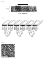
- FIG. 8 illustrates the main part of the sputtering source included in the AC sputtering system.
- the sputtering source includes a plurality of sputtering sections that respectively include plate-like targets 31a to 31f. When the surface of each target subjected to sputtering is referred to as "sputtering surface", each sputtering section is disposed so that the sputtering surface is positioned in the same plane.
- the targets 31a to 31f are formed to be elongated in the longitudinal direction, and have an identical shape.
- the targets 31a to 31f are disposed in parallel so that the edge area (side surface) of the sputtering surface in the longitudinal direction is positioned at an interval from the edge area of the sputtering surface of the adjacent target. Therefore, the side surfaces of the targets 31a to 31f are positioned parallel to each other.
- Alternating power sources 17a to 17c are disposed outside the vacuum chamber.
- One of the two terminals of each alternating power source (17a to 17c) is connected to one of two adjacent electrodes, and the other of the two terminals of each alternating power source is connected to the other of the two adjacent electrodes.
- the terminals of each alternating power source (17a to 17c) respectively output voltages that differ in polarity. Since the targets 31a to 31f are attached to the electrodes, AC voltages that differ in polarity are applied to the adjacent targets 31 a to 31f from the alternating power sources 17a to 17c. Therefore, a positive potential is applied to one of the adjacent targets, and a negative potential is applied to the other of the adjacent targets.
- Magnetic field-forming means 40a to 40f are disposed on the side of the electrodes opposite to the targets 31a to 31f.
- Each of the magnetic field-forming means 40a to 40f includes an elongated ring-like magnet having outer circumferential dimensions approximately equal to those of the targets 31a to 31f, and a rod-like magnet that is shorter than the ring-like magnet.
- the ring-like magnets are disposed in parallel to the longitudinal direction of the targets 31a to 31f at a position opposite to the corresponding target. Since the targets 31a to 31f are disposed in parallel at a given interval, the ring-like magnets are disposed at the given interval in the same manner as the targets 31a to 31f.
- the alternating current density when performing AC sputtering using an oxide target is preferably 3 to 20 W/cm 2 (3 W/cm 2 or more and 20 W/cm 2 or less). If the alternating current density is less than 3 W/cm 2 , it is not economical from the viewpoint of production due to a low deposition rate. If the alternating current density exceeds 20 W/cm 2 , the target may break. The alternating current density is more preferably 4 to 15 W/cm 2 .
- the partial pressure of water during AC sputtering is preferably 5 ⁇ 10 -3 to 5 ⁇ 10 -1 Pa. If the partial pressure of water is less than 5 ⁇ 10 -3 Pa, microcrystals may be formed in the thin film immediately after deposition, so that the Rrms of the thin film may become larger than 5.3 A. If the partial pressure of water exceeds 5 ⁇ 10 -1 Pa, the degree of 5s orbital overlap of In may decrease due to a significant decrease in film density, so that a decrease in mobility may occur.
- the partial pressure of water during sputtering is preferably 1 ⁇ 10 -2 to 1 ⁇ 10 -1 Pa when the alternating current density is 5 W/cm 2 .
- the AC sputtering frequency is preferably 10 kHz to 1 MHz. If the AC sputtering frequency is less than 10 kHz, noise may occur. If the AC sputtering frequency exceeds 1 MHz, sputtering may occur at a position other than the desired target position due to an increase in distribution of plasma, so that uniformity may be impaired.
- the AC sputtering frequency is more preferably 20 to 500 kHz.
- the sputtering conditions other than the above items may be appropriately selected.
- the amorphous oxide thin film obtained by the steps (1) and (2) is subjected to heat treatment (i.e., annealed) to obtain a crystalline oxide thin film. More specifically, the amorphous oxide thin film obtained by the steps (1) and (2) that has an Rrms (root-mean-square-roughness) of 1.0 to 5.3 A is crystallized to obtain an oxide layer (crystalline oxide thin film).
- the annealing temperature is preferably 150 to 400°C, and more preferably 200 to 350°C. If the annealing temperature is less than 150°C, crystallization may be insufficient. If the annealing temperature exceeds 500°C, the device may break.
- the annealing (crystallization) time is normally 10 minutes to 3.5 hours, and preferably 15 minutes to 2.5 hours.
- the dopants are dissolved in the indium oxide crystals, so that a single-phase bixbyite structure is obtained.
- the oxide layer it is preferable to crystallize the oxide layer before forming a protecting film. If the amorphous thin film is exposed to plasma, the subsequent crystallization process may be adversely affected by plasma damage, so that lattice defects or the like may occur in the film.
- the atmosphere employed when subjecting the amorphous oxide thin film to the heat treatment (annealing) is not particularly limited, but is preferably air or an oxygen atmosphere from the viewpoint of carrier control.
- the oxide thin film may be subjected to the heat treatment (annealing) in the presence or absence of oxygen using a lamp annealing system, a laser annealing system, a thermal plasma system, a hot-blast heating system, a contact heating system, or the like.
- the crystals of the oxide thin film are arranged in a columnar shape from the surface of the substrate to the surface of the sample.
- the oxide thin film in which the crystals are arranged in a columnar shape has a small crystal misorientation and a low trap density, a TFT that exhibits improved field-effect mobility and a good S-factor can be formed with high reproducibility. It is also possible to control the carrier concentration to 10 18 /cm 3 or less due to a small number of oxygen defects (deficiencies).
- the crystals are grown from the substrate in a columnar shape during the heat treatment (annealing) step.
- annealing heat treatment
- the crystals are arranged in a columnar shape on surface of the substrate, crystal growth is not hindered by microcrystals during the annealing (crystallization) step. Therefore, the crystal diameter increases as compared with a thin film that is formed without introducing water, and the average crystal diameter becomes 1 ⁇ m or more.
- the oxide semiconductor thin film (oxide layer) after annealing (crystallization) have an average crystal diameter of 1 to 27 ⁇ m. It is more preferable that the thin film have an average crystal diameter of 1.3 to 27 ⁇ m, and particularly preferably 2.1 to 27 ⁇ m. If the average crystal diameter of the thin film is less than 1 ⁇ m, microcrystals may have been formed in the thin film when forming the thin film. If the average crystal diameter of the thin film exceeds 27 ⁇ m, a variation in TFT characteristics may occur due to scattering of carriers at the crystal grain boundaries.
- the amorphous film having an Rrms of 1.0 to 5.3 A immediately after deposition is crystallized by the heat treatment (annealing).
- the crystallized oxide thin film (oxide layer) substantially has an In 2 O 3 bixbyite structure.
- substantially has an In 2 O 3 bixbyite structure means that the oxide layer (crystalline oxide thin film) exhibits the effects of the invention due to the bixbyite structure, or 70% or more (preferably 80% or more, and more preferably 85% or more) of the crystal structure of the crystalline oxide thin film has a bixbyite structure.
- the oxide layer (oxide thin film) included in the stacked layer structure obtained by the method according to the invention is a thin film formed of indium and oxygen, a thin film formed of indium, oxygen, and gallium, a thin film formed of indium, oxygen, and aluminum, a thin film formed of indium, oxygen, and zinc, or a thin film formed of indium, oxygen, and tin.
- the oxide layer may include unavoidable impurities as long as the oxide layer mainly include the above elements. Note that it is desirable that the crystal structure substantially have only an indium oxide bixbyite structure.
- a thin film having an indium oxide bixbyite structure that is obtained by controlling the Rrms of the oxide thin film (oxide layer) to 1.0 to 5.3 A, and then annealing (crystallizing) the oxide thin film (oxide layer) has a configuration in which the crystals of the oxide thin film are arranged in a columnar shape from the surface of the substrate to the surface of the thin film, excellent TFT characteristics can be achieved.
- the oxide thin film (oxide layer) has an indium oxide bixbyite structure may be determined by X-ray diffraction (XRD) measurement.
- XRD X-ray diffraction
- the optical path difference of X-rays scattered at each position is an integral multiple of the wavelength of the X-rays, the amplitude of the waves increases since the phases of the waves coincide, so that the diffraction phenomenon occurs.
- the type of compound can be identified by utilizing X-ray diffraction. It is also possible to evaluate the size of crystals (crystalline order), the distribution state of the orientation of crystals present in the material (crystal orientation), and the residual stress applied to the crystals.
- the density of the oxide layer (oxide thin film) obtained by the method according to the invention is preferably 6.2 g/cm 3 or more, and more preferably 6.4 g/cm 3 or more. If the density of the oxide layer (oxide thin film) is less than 6.2 g/cm 3 , the degree of 5s orbital overlap of In that takes part in carrier conduction may decrease, so that a decrease in mobility may occur. It is preferable that the oxide layer (oxide thin film) obtained by the method according to the invention have a high density.
- the density of the oxide layer (oxide thin film) obtained by the method according to the invention is particularly preferably set to 6.2 to 7.1 g/cm 3 .
- a stacked layer structure produced by the method according to the invention has the same structure and properties as those of the stacked layer structure according to the invention.
- the oxide thin film according to the invention and a stacked layer structure produced by the method according to the invention may be used for a thin film transistor.
- the oxide layer included in the stacked layer structure may be used as a channel layer.
- the thin film transistor according to the invention includes the oxide layer and the insulating layer included in the stacked layer structure according to the invention as a channel layer and a gate insulating film, respectively, and also includes a protecting film that includes SiN x or the like on the oxide layer.
- the channel layer included in the thin film transistor according to the invention is formed of the oxide layer included in the stacked layer structure according to the invention.
- the oxide layer (channel layer) has the above configuration and the like.
- the gate insulating film included in the thin film transistor according to the invention is formed of the insulating layer included in the stacked layer structure according to the invention.
- the insulating layer (gate insulating film) has the above configuration and the like.
- the oxide layer included in the stacked layer structure according to the invention is a crystalline oxide thin film having a controlled crystal orientation and crystal diameter.
- oxygen defects deficiencies
- CVD chemical vapor deposition
- the thickness of the channel layer of the thin film transistor according to the invention is normally 10 to 300 nm, preferably 20 to 250 nm, more preferably 30 to 200 nm, still more preferably 35 to 120 nm, and particularly preferably 40 to 80 nm. If the thickness of the channel layer is less than 10 nm, an in-plane non-uniformity in TFT characteristics may occur due to non-uniformity in thickness when forming the channel layer over a large area. If the thickness of the channel layer exceeds 300 nm, it may take time to form the channel layer (i.e., industrial application may be difficult).
- the channel layer included in the thin film transistor according to the invention is normally used as an N-type region, and may be used for various semiconductor devices (e.g., PN-junction transistor) in combination with a p-type semiconductor (e.g., P-type Si semiconductor, P-type oxide semiconductor, or P-type organic semiconductor).
- PN-junction transistor e.g., PN-junction transistor
- a p-type semiconductor e.g., P-type Si semiconductor, P-type oxide semiconductor, or P-type organic semiconductor.
- the protecting film included in the thin film transistor according to the invention preferably includes SiN x .
- SiN x can form a dense film as compared with SiO 2 , and can suppress a deterioration in TFT.
- the protecting film may be stacked on the channel layer.
- the protecting film can be formed directly on the channel layer without forming a buffer layer by utilizing the oxide layer included in the stacked layer structure according to the invention as the channel layer. This makes it possible to simplify the production process.
- the protecting film may include SiO 2 , Al 2 O 3 , Ta 2 O 5 , TiO 2 , MgO, ZrO 2 , CeO 2 , K 2 O, Li 2 O, Na 2 O, Rb 2 O, Sc 2 O 3 , Y 2 O 3 , HfO 2 , CaHfO 3 , PbTi 3 , BaTa 2 O 6 , Sm 2 O 3 , SrTiO 3 , AlN, or the like in addition to SiN x . It is preferable that the protecting film substantially include only SiN x .
- the expression “substantially include only SiN x” means that 70 wt% or more (preferably 80 wt% or more, and more preferably 85 wt% or more) of the thin film that forms the protecting film included in the thin film transistor according to the invention is SiN x .
- the oxide semiconductor film it is preferable to subject the oxide semiconductor film to an ozone treatment, an oxygen plasma treatment, a nitrogen dioxide plasma treatment, or a nitrous oxide plasma treatment as a pretreatment before forming the protecting film.
- the above treatment may be performed on the oxide semiconductor film at an arbitrary timing before forming the protecting film. Note that it is desirable to perform the above treatment immediately before forming the protecting film. This makes it possible to suppress occurrence of oxygen defects in the oxide semiconductor film.
- An In-OH bond in the crystal structure is stabilized by subjecting the oxide semiconductor film to an ozone treatment, an oxygen plasma treatment, a nitrogen dioxide plasma treatment, or a nitrous oxide plasma treatment, so that diffusion of hydrogen in the oxide semiconductor film can be suppressed.
- the gate insulating film is formed by plasma chemical vapor deposition (CVD), for example.
- CVD plasma chemical vapor deposition
- the gate insulating film is formed by plasma CVD, and the oxide semiconductor layer is formed on the gate insulating film, hydrogen contained in the gate insulating film may be diffused into the oxide semiconductor layer, so that a deterioration in crystallinity of the oxide semiconductor layer or a deterioration in reliability of the TFT may occur.
- the thickness of the gate insulating film is normally 5 to 400 nm, and preferably 50 to 300 nm.
- a material used to form each electrode (i.e., drain electrode, source electrode, and gate electrode) included in the thin film transistor according to the invention is not particularly limited.
- a known material may be arbitrarily selected as the material used to form each electrode.
- a transparent electrode material e.g., ITO, IZO, ZnO, or SnO 2
- a metal electrode material e.g., Al, Ag, Cu, Cr, Ni, Mo, Au, Ti, or Ta
- an alloy thereof may be used to form each electrode.
- Each electrode i.e., drain electrode, source electrode, and gate electrode
- the source/drain electrode may have a structure in which a good conductor such as Al or Cu is sandwiched between a metal that exhibits excellent adhesion (e.g., Ti or Mo), since a reduction in resistance is strongly desired.
- a good conductor such as Al or Cu
- a metal that exhibits excellent adhesion e.g., Ti or Mo
- the thin film transistor according to the invention may be used as a field effect transistor, and may also be applied to an integrated circuit (e.g., logic circuit, memory circuit, and differential amplifier circuit).
- the thin film transistor according to the invention may also be used as a static induction transistor, a Schottky barrier transistor, a Schottky diode, and a resistor element.
- the thin film transistor according to the invention may have an arbitrary known configuration (e.g., bottom gate configuration, bottom contact configuration, or top contact configuration). It is advantageous that the thin film transistor have a bottom gate configuration since high performance can be achieved as compared with an amorphous silicon or ZnO thin film transistor. Moreover, since the number of masks used during the production can be reduced, the production cost can be reduced (e.g., when producing a large display).
- the thin film transistor according to the invention may suitably be used for a display apparatus. It is preferable that the thin film transistor be a channel-etch thin film transistor having a bottom gate configuration when used for a large-area display. When using a channel-etch thin film transistor having a bottom gate configuration, a display panel can be produced at low cost since the number of photomasks used during photolithography can be reduced. It is particularly preferable that the thin film transistor be a channel-etch thin film transistor having a bottom gate-top contact configuration from the viewpoint of an increase in mobility and the like, and ease of industrial production.
- a 4-inch target formed of an oxide having the composition shown in Table 1, and a slide ("#1737" manufactured by Corning) as a substrate (insulating layer included in stacked layer structure) were placed in a magnetron sputtering system.
- An amorphous film having a thickness of 50 nm was formed on the slide by DC magnetron sputtering under the following conditions.
- Ar gas, O 2 gas, and H 2 O gas were introduced when forming the amorphous film in the partial pressure ratio shown in Table 1.
- the substrate on which the amorphous film was formed was heated at 300°C for 1 hour in air to crystallize the amorphous film to obtain an oxide semiconductor film (oxide layer included in stacked layer structure).
- a conductive silicon substrate provided with a thermal oxide film (thickness: 100 nm) was used as a substrate.
- the sputtering conditions were the same as those employed in [1].
- the thermal oxide film functions as a gate insulating film (insulating layer included in stacked layer structure), and the conductive silicon functions as a gate electrode.
- An amorphous thin film having a thickness of 50 nm was formed on the gate insulating film by sputtering under the conditions shown in Table 1.
- a resist (“OFPR #800” manufactured by Tokyo Ohka Kogyo Co., Ltd.) was applied to the amorphous thin film, pre-baked (80°C, 5 minutes), and exposed. The resist was then developed, post-baked (120°C, 5 minutes), and etched using oxalic acid to pattern the resist into the desired shape.
- the thin film was then annealed at 300°C for 1 hour in a hot-blast heating furnace to crystallize the thin film.
- An Mo film (200 nm) was then formed by sputtering. Source/drain electrodes having the desired shape were patterned by channel etching. An SiN x film (protecting film) was then formed by plasma-enhanced CVD (PECVD). A contact hole was formed using hydrofluoric acid to obtain a thin film transistor.
- the field-effect mobility ( ⁇ ), the S-factor, and the threshold voltage (Vth) of the thin film transistor were evaluated.
- the field-effect mobility ( ⁇ ), the S-factor, and the threshold voltage (Vth) were measured at room temperature in a shading environment (in a shield box) using a semiconductor parameter analyzer ("4200SCS" manufactured by Keithley Instruments Inc.).
- the drain voltage (Vd) was set to 10 V. The results are shown in Table 1.
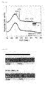
- FIG 1 shows the X-ray diffraction chart of the thin films of Examples 1 to 3 immediately after deposition. A diffraction peak was not observed (i.e., the thin film was amorphous) immediately after deposition. A diffraction peak was observed (i.e., the thin film was crystallized) after annealing at 300°C for 1 hour in air.
- FIG 2 shows the X-ray diffraction chart of the thin films of Examples 1 to 3 after annealing.
- indium oxide bixbyite structure was observed in the crystallized thin films of Examples 1 to 3.
- the indium oxide bixbyite crystal structure is listed on a Joint Committee of Powder Diffraction Standards (JCPDS) card.
- JCPDS card No. of the indium oxide bixbyite structure is 06-0416.
- the thin films of Examples 4 to 13 were also amorphous immediately after deposition, and only an indium oxide bixbyite structure was observed after annealing at 300°C for 1 hour in air.
- the Rrms (in a 20 ⁇ 20 ⁇ m 2 area) of the surface of the thin film of Example 1 formed on the glass substrate was measured immediately after deposition using an AFM system ("JSPM-4500" manufactured by JEOL Ltd.), and found to be 2.3 A (i.e., very flat).
- Table 1 also shows the Rrms of the thin films of Examples 2 to 13.
- FIG. 3 shows the SIM image of the thin film of Example 1 after annealing (crystallization) at 300°C for 1 hour. Note that FIG. 3 is a partial enlarged view of the SIM image (35 ⁇ 35- ⁇ m square area) at a magnification of 10,000. Crystal grains were observed, and the average crystal diameter was 2.1 ⁇ m.
- the average crystal diameter of the oxide semiconductor thin film was determined by measuring the maximum diameter of each crystal grain observed within a 35 ⁇ 35- ⁇ m square area, and calculating the average value of the maximum diameters.
- the average crystal diameter of the thin films of Examples 2 to 13 is shown in Table 1.
- FIG. 4 shows the cross-sectional TEM image of the thin film of Example 1 after annealing (crystallization) at 300°C for 1 hour. Note that FIG. 4 is a partial enlarged view of the oxide thin film within a 1 ⁇ 1- ⁇ m square field of view at a magnification of 100,000. As shown in FIG. 4 , the crystals were arranged in a columnar shape from the surface of the substrate to the surface of the sample. In the thin films of Examples 2 to 13, the crystals were also arranged in a columnar shape from the surface of the substrate to the surface of the sample.
- a thin film transistor and a thin film evaluation device were fabricated, and evaluated in the same manner as in Example 1, except that the target used to form the oxide semiconductor film, the sputtering conditions, and the annealing conditions were changed as shown in Table 2. The results are shown in Table 2.
- FIG. 5 shows the X-ray diffraction chart of the thin film of Comparative Example 1.
- a diffraction peak was observed (i.e., the thin film was crystallized) immediately after deposition.
- the half-width of the diffraction peak increased due to annealing at 300°C for 1 hour in air.
- the thin films of Comparative Examples 4 and 6 were amorphous immediately after deposition, and crystallized after annealing at 300°C for 1 hour in air. Only an indium oxide bixbyite structure was observed in the thin films of Comparative Examples 4 and 6.
- the Rrms (in a 20 ⁇ 20 ⁇ m 2 area) of the surface of the thin film of Comparative Example 1 formed on the glass substrate was measured immediately after deposition using an AFM system ("JSPM-4500" manufactured by JEOL Ltd.), and found to be 8.6 A (i.e., the surface of the thin film of Comparative Example 1 was rough as compared with Examples 1 to 13).
- Table 2 also shows the Rrms of the thin films of Comparative Examples 2 to 7.
- the thin film of Comparative Example 1 formed on the glass substrate was subjected to SIM measurement in the same manner as in Examples 1 to 13.
- a focused ion beam system "FB-2100" manufactured by Hitachi, Ltd.
- the accelerating voltage was set to 40 kV.
- FIG 6 shows the SIM image of the thin film of Comparative Example 1 after annealing (crystallization) at 300°C for 1 hour. Note that FIG. 6 is a partial enlarged view of the SIM image (35 ⁇ 35- ⁇ m square area) at a magnification of 10,000. Crystal grains were observed, and the average crystal diameter was 0.57 ⁇ m.
- the average crystal diameter of the oxide semiconductor thin film was determined by measuring the maximum diameter of each crystal grain observed within a 35 ⁇ 35- ⁇ m square area, and calculating the average value of the maximum diameters.
- the average crystal diameter of the thin films of Comparative Examples 2 to 7 is shown in Table 2.
- the average crystal diameter of the thin films of Comparative Examples 2 to 7 was less than 1 ⁇ m.
- the thin film of Comparative Example 1 formed on the glass substrate was subjected to cross-sectional TEM measurement in the same manner as in Examples 1 to 13.
- a field emission transmission electron microscope "HF-2100" manufactured by Hitachi, Ltd.
- the accelerating voltage was set to 200 kV.
- FIG 7 shows the cross-sectional TEM image of the thin film of Comparative Example 1 after annealing at 300°C for 1 hour. Note that FIG 7 is a partial enlarged view of the oxide thin film within a 1 ⁇ 1- ⁇ m square field of view at a magnification of 100,000. As shown in FIG 7 , microcrystals were observed in the thin film of Comparative Example 1. Microcrystals were also observed in the thin films of Comparative Examples 2 to 7.
- the Hall effect measurement device was placed in a "ResiTest 8300" system (manufactured by Toyo Corporation), and the Hall effect was evaluated at room temperature. The results are shown in Table 2.
- the carrier concentration in the thin films of Comparative Examples 1 to 7 was more than 10 18 cm -3 . It was thus found that the thin films of Comparative Examples 1 to 7 had a large number of oxygen defects.
- the field-effect mobility ( ⁇ ), the S-factor, and the threshold voltage (Vth) of the thin film transistor were measured at room temperature in a shading environment (in a shield box) using a semiconductor parameter analyzer ("4200SCS" manufactured by Keithley Instruments Inc.). The drain voltage (Vd) was set to 10 V. The results are shown in Table 2. As shown in Table 2, the devices of Comparative Examples 1 to 7 had normally-on properties since the carrier concentration was more than 10 18 cm -3 .
- Example 1 Example 2
- Example 3 Example 4
- Example 5 Example 6
- Example 7 Composition of target In 2 O 3 In 2 O 3 In 2 O 3 In 2 O 3
- Ultimate pressure (Pa) 8.5 ⁇ 10 -5 8.5 ⁇ 10 -5 8.5 ⁇ 10 -5 8.5 ⁇ 10 5 8.5 ⁇ 10 -5 8.5 ⁇ 10 -5 Sputtering pressure (Pa) 0.4 0.4 0.4 0.4 0.4 0.4 0.4 0.4 0.4 0.4 0.4 0.4 0.4 0.4 0.4 0.4 0.4 0.4 0.4 [H 2 O]/([H 2 O]+[Ar]+[O 2 ]) (%) 1 2 6 1 2 1 2 [Ar]/([H 2 O]+[Ar]+[O 2 ]) (%) 99 98 94 97 95 99 98 [O 2 ]/([H 2 O]+[Ar]+[O 2 ]) (%) 0 0 0 2
- a thin film transistor and a thin film evaluation device were fabricated, and evaluated in the same manner as in Example 1, except that the amorphous film was formed by AC sputtering under the conditions shown in Table 3 using the system disclosed in JP-A-2005-290550 , and annealed. The results are shown in Table 3.
- AC sputtering was performed using the system illustrated in FIG. 8 .
- the width of the magnetic field-forming means 40a to 40f was the same as that (200 mm) of the targets 31a to 31f.
- Ar and H 2 O sputtering gas
- the pressure of the atmosphere was 0.5 Pa.
- An indium zinc oxide (IZO) film was formed for 10 seconds under the above conditions. The thickness of the IZO film was measured, and found to be 15 nm. The IZO film was formed at a high rate of 90 nm/min (i.e., it is suitable for mass production).
- the glass substrate provided with the IZO film was put in an electric furnace, annealed at 400°C for 15 minutes in air, cut to a size of 1 cm 2 , and subjected to Hall measurement using a four probe method. It was found that the carrier concentration was 1.5 ⁇ 10 16 cm -3 (i.e., the film had sufficient semiconductivity).
- a semiconductor thin film was obtained in the same manner as in Example 14, except that the composition of the target and the sputtering conditions were changed as shown in Table 3.
- a thin film transistor and a thin film evaluation device were fabricated, and evaluated in the same manner as in Example 14. It was found by Hall measurement that a semiconductor was obtained. The results are shown in Table 3.
- a film was formed while increasing the output power (alternating current density) to 22 W/cm 2 .
- the film was thus formed at a rate of 75 nm/min.
- the crystals were not arranged in a columnar shape with respect to the surface of the sample, and the carrier concentration was 7.5 ⁇ 10 18 cm -3 (i.e., a semiconductor was not obtained).
- a 4-inch target having the composition shown in Table 4, a conductive silicon substrate provided with a thermal oxide film (thickness: 100 nm), a conductive silicon substrate, and a slide ("#1737" manufactured by Corning) as a substrate were placed in a magnetron sputtering system.
- An SiO x film (insulating layer) was formed on the conductive silicon substrate by CVD to a thickness of 100 nm. The insulating layer was then subjected to an ozone treatment, an oxygen plasma treatment, or a nitrogen dioxide plasma treatment (see Table 4).
- An amorphous film having a thickness of 50 nm was formed on the conductive silicon substrate provided with a thermal oxide film (thickness: 100 nm), the conductive silicon substrate provided with the SiO x film (thickness: 100 nm) formed by CVD, and the slide by DC magnetron sputtering under the following conditions.
- Ar gas, O 2 gas, and H 2 O gas were introduced when forming the amorphous film in the partial pressure ratio shown in Table 4.
- the amorphous film was crystallized using the partial pressure ratio of oxygen, the temperature increase rate, the heat treatment temperature, and the heat treatment time shown in Table 4 to obtain an oxide semiconductor film.
- the Hall effect measurement device was placed in a "ResiTest 8300" system (manufactured by Toyo Corporation), and the Hall effect was evaluated at room temperature.
- the SiO x film functions as a gate insulating film, and the conductive silicon functions as a gate electrode.
- the SiO x film was subjected to an ozone treatment, an oxygen plasma treatment, or a nitrogen dioxide plasma treatment (see Table 4).
- An amorphous thin film having a thickness of 50 nm was formed on the gate insulating film by sputtering under the conditions shown in Table 4.
- a resist (“OFPR #800" manufactured by Tokyo Ohka Kogyo Co., Ltd.) was applied to the amorphous thin film, pre-baked (80°C, 5 minutes), and exposed.
- the resist was then developed, post-baked (120°C, 5 minutes), and etched using oxalic acid to pattern the resist into the desired shape.
- the thin film was then annealed using the partial pressure ratio of oxygen, the temperature increase rate, the heat treatment temperature, and the heat treatment time shown in Table 4 to crystallize the thin film. It was confirmed by ICP-AES analysis that the atomic ratio of the elements contained in the crystallized oxide thin film was the same as that of the sputtering target.
- An Mo film (200 nm) was then formed by sputtering. Source/drain electrodes having the desired shape were patterned by channel etching. The oxide semiconductor film was subjected to an ozone treatment, an oxygen plasma treatment, or a nitrogen dioxide plasma treatment (see Table 4) as a pretreatment before forming a protecting film. An SiN x film (protecting film) was then formed by plasma-enhanced CVD (PECVD). A contact hole was formed using hydrofluoric acid to obtain a thin film transistor.
- PECVD plasma-enhanced CVD
- the field-effect mobility ( ⁇ ), the S-factor, and the threshold voltage (Vth) of the thin film transistor were evaluated.
- the field-effect mobility ( ⁇ ), the S-factor, and the threshold voltage (Vth) were measured at room temperature in a shading environment (in a shield box) using a semiconductor parameter analyzer ("4200SCS" manufactured by Keithley Instruments Inc.).
- the drain voltage (Vd) was set to 10 V. The results are shown in Table 4.
- FIG 9 shows the EBSP image quality (IQ) map of the thin film of Example 19.
- IQ image quality
- Grain boundaries having a misorientation of 2° or more and less than 5°, or 5° or more and less than 15° were mainly observed.
- the ratio of each grain boundary to the total grain boundaries was calculated.
- the ratio of grain boundaries having a misorientation of 2° or more and less than 5° was 43.5%
- the ratio of grain boundaries having a misorientation of 5° or more and less than 15° was 36.0%
- the ratio of grain boundaries having a misorientation of 15° or more and less than 180° was 20.5%. Therefore, the ratio of grain boundaries having a misorientation of 2° or more and less than 15° to the total grain boundaries was 79.5%.
- the ratio of grain boundaries having a misorientation of 2° or more and less than 15° to the total grain boundaries was 60 to 90%.
- FIG 11 shows the EBSP orientation map of the thin film of Example 19.
- the dimensions of the measurement area were 40 ⁇ 40 ⁇ m, and the step size was 0.2 ⁇ m.
- the dense crystal grain structure and the crystal orientations ((111), (001), and (101)) were observed corresponding to the grain boundaries having a misorientation of 2° or more and less than 5°, the grain boundaries having a misorientation of 5° or more and less than 15°, and the grain boundaries having a misorientation of 15° or more and less than 180°.
- FIG 12 shows a map in which the measurement points are indicated by dots on the inverse pole figure of Example 19. The (111), (001), and (101) orientations were observed in the same manner as in the orientation map.
- the crystal structure of the thin film of Examples 19 to 27 formed on the glass substrate was determined using an X-ray diffraction measurement system ("Ultima-III" manufactured by Rigaku Corporation). A diffraction peak was not observed (i.e., the thin film was amorphous) immediately after deposition. A diffraction peak was observed (i.e., the thin film was crystallized) after annealing performed under the conditions shown in Table 4. As a result of analyzing the X-ray diffraction chart, only an indium oxide bixbyite structure was observed in the crystallized thin films of Examples 19 to 27. The indium oxide bixbyite crystal structure is listed on a JCPDS card. The JCPDS card No. of the indium oxide bixbyite structure is 06-0416.
- the Rrms (in a 20 ⁇ 20 ⁇ m 2 area) of the surface of the thin film of Example 19 formed on the glass substrate was measured immediately after deposition using an AFM system ("JSPM-4500" manufactured by JEOL Ltd.), and found to be 1.8 ⁇ (i.e., very flat).
- Table 4 also shows the Rrms of the thin films of Examples 20 to 27.
- the thin films of Examples 19 to 27 formed on the glass substrate were subjected to cross-sectional TEM measurement.
- a field emission transmission electron microscope "HF-2100" manufactured by Hitachi, Ltd. was used for the measurement.
- the accelerating voltage was set to 200 kV.
- a state in which the crystals were arranged in a columnar shape from the surface of the substrate to the surface of the sample was observed in the same manner as in Examples 1 to 18.
- Example 19 Example 20
- Example 21 Example 22
- a thin film transistor and a thin film evaluation device were fabricated, and evaluated in the same manner as in Examples 19 to 27, except that the target used to form the oxide semiconductor film, the sputtering conditions, and the annealing conditions were changed as shown in Table 5, and the oxide semiconductor film was not subjected to the ozone treatment, the oxygen plasma treatment, or the nitrogen dioxide plasma treatment. The results are shown in Table 5.
- FIG. 13 shows the EBSP image quality (IQ) map of the thin film of Comparative Example 9.
- IQ EBSP image quality
- FIG. 13 shows the EBSP image quality (IQ) map of the thin film of Comparative Example 9.
- a microstructure was not observed in the crystal grains, differing from Examples 19 to 27. Since the crystal grains were small, the dimensions of the measurement area were changed to 0.5 ⁇ 0.5 ⁇ m, and the step size was changed to 0.005 ⁇ m.
- EBSP orientation mapping was performed to divide the area into an area having a misorientation of 2° or more and less than 5°, an area having a misorientation of 5° or more and less than 15°, and an area having a misorientation of 15° or more and less than 180°.
- FIG. 14 shows the misorientation data.
- the average crystal diameter was analyzed using an area enclosed by components having a misorientation of 15° or more as a crystal grain, and found to be 0.137 ⁇ m.
- the average crystal diameter measured in Comparative Examples 10 to 13 was also less than 1.0 ⁇ m.
- Grain boundaries having a misorientation of 2° or more and less than 5°, or 5° or more and less than 15°, were observed to only a small extent.
- the ratio of each grain boundary to the total grain boundaries was calculated.
- the ratio of grain boundaries having a misorientation of 2° or more and less than 5° was 9.6%
- the ratio of grain boundaries having a misorientation of 5° or more and less than 15° was 5.4%
- the ratio of grain boundaries having a misorientation of 15° or more and less than 180° was 85%.
- the ratio of grain boundaries having a misorientation of 2° or more and less than 15° the total grain boundaries was 15.0%.
- the ratio of grain boundaries having a misorientation of 2° or more and less than 15° to the total grain boundaries was less than 60%.
- FIG. 15 shows the EBSP orientation map of the thin film of Comparative Example 9. Since the crystal grains were small, the dimensions of the measurement area were changed to 0.5 ⁇ 0.5 ⁇ m, and the step size was changed to 0.005 ⁇ m. A microstructure was not observed since grain boundaries having a misorientation of 2° or more and less than 5°, or 5° or more and less than 15°, were not observed. The crystal grains showing (111) preferential orientation were observed corresponding to the grain boundaries having a misorientation of 15° or more and less than 180°.
- FIG 16 shows a map in which the measurement points are indicated by dots on the inverse pole figure of Comparative Example 9. The (111) preferential orientation was observed in the same manner as in the orientation map.
- the crystal structure of the thin film formed on the glass substrate was determined in the same manner as in Examples 19 to 27 using an X-ray diffraction measurement system ("Ultima-III" manufactured by Rigaku Corporation). A diffraction peak was observed for the thin films of Comparative Examples 9 to 13 (i.e., the thin film was crystallized) immediately after deposition. The thin film was annealed immediately after deposition under the conditions shown in Table 5. As a result of analyzing the X-ray diffraction chart, only an indium oxide bixbyite structure was observed in the thin films of Comparative Examples 9 to 13. The indium oxide bixbyite crystal structure is listed on a JCPDS card. The JCPDS card No. of the indium oxide bixbyite structure is 06-0416.
- the Rrms (in a 20 ⁇ 20 ⁇ m 2 area) of the surface of the thin film of Comparative Example 9 formed on the glass substrate was measured immediately after deposition using an AFM system ("JSPM-4500" manufactured by JEOL Ltd.), and found to be 8.6 ⁇ (i.e., the surface of the thin film of Comparative Example 9 was rough as compared with Examples 19 to 27).
- Table 5 also shows the Rrms of the thin films of Comparative Examples 10 to 13.
- the Hall effect measurement device was placed in a "ResiTest 8300" system (manufactured by Toyo Corporation), and the Hall effect was evaluated at room temperature. The results are shown in Table 5.
- the carrier concentration in the thin films of Comparative Examples 9 to 13 was more than 10 18 cm -3 . It was thus found that the thin films of Comparative Examples 9 to 13 had a large number of oxygen defects.
- the field-effect mobility ( ⁇ ), the S-factor, and the threshold voltage (Vth) of the thin film transistor were measured at room temperature in a shading environment (in a shield box) using a semiconductor parameter analyzer ("4200SCS" manufactured by Keithley Instruments Inc.). The drain voltage (Vd) was set to 10 V. The results are shown in Table 5. As shown in Table 5, the devices of Comparative Examples 9 to 13 had normally-on properties since the carrier concentration was more than 10 18 cm -3 .
- a 4-inch target having the composition shown in Table 6, a conductive silicon substrate provided with a thermal oxide film (thickness: 100 nm), and a slide ("#1737" manufactured by Corning) as a substrate were placed in a magnetron sputtering system.
- An amorphous film having a thickness of 50 nm was formed on the silicon substrate provided with a thermal oxide film (thickness: 100 nm) and the slide by DC magnetron sputtering under the following conditions. Ar gas, O 2 gas, and H 2 O gas were introduced when forming the amorphous film in the partial pressure ratio shown in Table 6.
- the amorphous film was crystallized using the partial pressure ratio of oxygen, the heat treatment temperature, and the heat treatment time shown in Table 6 to obtain an oxide semiconductor film. It was confirmed by ICP-AES analysis that the atomic ratio of the elements contained in the crystallized oxide thin film was the same as that of the sputtering target.
- the Hall effect measurement device was placed in a "ResiTest 8300" system (manufactured by Toyo Corporation), and the Hall effect was evaluated at room temperature. The results are shown in Table 6.
- a conductive silicon substrate provided with a thermal oxide film (SiO x ) (thickness: 100 nm) was used as a substrate.
- the SiO x film functions as a gate insulating film, and the conductive silicon functions as a gate electrode.
- An amorphous thin film having a thickness of 50 nm was formed on the gate insulating film by sputtering under the conditions shown in Table 6.
- a resist (“OFPR #800" manufactured by Tokyo Ohka Kogyo Co., Ltd.) was applied to the amorphous thin film, pre-baked (80°C, 5 minutes), and exposed.
- the resist was then developed, post-baked (120°C, 5 minutes), and etched using oxalic acid to pattern the resist into the desired shape.
- the thin film was then annealed using the partial pressure ratio of oxygen, the heat treatment temperature, and the heat treatment time shown in Table 6 to crystallize the thin film. It was confirmed by ICP-AES analysis that the atomic ratio of the elements contained in the crystallized oxide thin film was the same as that of the sputtering target.
- FIG 17 illustrates the shape of the device.
- the field-effect mobility ( ⁇ ), the S-factor, and the threshold voltage (Vth) of the thin film transistor were evaluated.
- the field-effect mobility ( ⁇ ), the S-factor, and the threshold voltage (Vth) were measured at room temperature in a shading environment (in a shield box) using a semiconductor parameter analyzer ("4200SCS" manufactured by Keithley Instruments Inc.).
- FIG. 18 shows the transfer characteristics of the thin film transistor of Example 28 (drain voltage: 0.1, 1.0, or 10 V).
- the field-effect mobility, the S-factor, and the threshold voltage of the thin film transistor (drain voltage: 10 V) were evaluated.
- the field-effect mobility, the S-factor, and the threshold voltage were evaluated at a drain voltage of 10 V. The results are shown in Table 6.
- FIG 19 shows the X-ray diffraction chart of the thin film of Example 28 immediately after deposition and after annealing. A diffraction peak was not observed (i.e., the thin film was amorphous) immediately after deposition. A diffraction peak was observed (i.e., the thin film was crystallized) after annealing.
- FIG. 19 shows the X-ray diffraction chart of the thin film of Example 28 after annealing.
- Example 28 As a result of analyzing the X-ray diffraction chart, only an indium oxide bixbyite structure was observed in the crystallized thin film of Example 28.
- the indium oxide bixbyite crystal structure is listed on a Joint Committee of Powder Diffraction Standards (JCPDS) card.
- JCPDS card No. of the indium oxide bixbyite structure is 06-0416.
- the thin films of Examples 29 to 33 were amorphous immediately after deposition in the same manner as the thin film of Example 28, and only an indium oxide bixbyite structure was observed after annealing.
- the Rrms (in a 20 ⁇ 20 ⁇ m 2 area) of the surface of the thin film of Example 28 formed on the glass substrate was measured immediately after deposition using an AFM system ("JSPM-4500" manufactured by JEOL Ltd.), and found to be 1.8 ⁇ (i.e., very flat).
- the Rrms of the thin films of Examples 29 to 33 was measured in the same manner as described above. The results are shown in Table 6.
- the thin film of Example 28 formed on the glass substrate was subjected to SIM measurement.
- a focused ion beam system "FB-2100" manufactured by Hitachi, Ltd. was used for the measurement.
- the accelerating voltage was set to 40 kV.
- the average crystal diameter determined by analyzing the thin film of Example 28 after annealing (crystallization) was 9.3 ⁇ m.
- the average crystal diameter of the oxide semiconductor thin film was determined by measuring the maximum diameter of each crystal grain observed within a 35 ⁇ 35- ⁇ m square area, and calculating the average value of the maximum diameters.
- the average crystal diameter of the thin films of Examples 29 to 33 was measured in the same manner as described above. The results are shown in Table 6.
- the thin film of Example 28 formed on the glass substrate was subjected to cross-sectional TEM measurement.
- a field emission transmission electron microscope "HF-2100" manufactured by Hitachi, Ltd.
- the accelerating voltage was set to 200 kV.
- FIG 20 shows the cross-sectional TEM image of the thin film of Example 28 immediately after deposition and after annealing (crystallization). Note that FIG 20 is a partial enlarged view of the oxide thin film within a 1 ⁇ 1- ⁇ m square field of view at a magnification of 50,000. As shown in FIG 20 , the thin film of Example 28 immediately after deposition was amorphous.
- the thin film of Example 28 formed on the silicon substrate provided with a thermal oxide film was subjected to KFM measurement.
- An E-sweep environmental control unit/NanoNavi probe station was used for the measurement.
- the dimensions of the measurement area were 25 ⁇ 25 ⁇ m, and the measurement was performed at room temperature.
- FIG 21 shows the surface potential profile of the thin film of Example 28 after annealing (crystallization).
- the potential difference between the maximum value and the minimum value of the surface potential of the thin film of Example 28 was 19.54 mV (i.e., 30 mV or less).
- the thin films of Examples 29 to 33 were also subjected to the KFM measurement in the same manner as described above.
- the potential difference between the maximum value and the minimum value of the surface potential of the thin films of Examples 29 to 33 in the 25 ⁇ 25- ⁇ m measurement area was 30 mV or less.
- Table 6 The results are shown in Table 6.
- the oxide layer and the insulating layer included in the stacked layer structure according to the invention are respectively used as the channel layer and the gate insulating film of a thin film transistor, a protecting film can be formed directly on the channel layer without providing a buffer layer. Therefore, the stacked layer structure according to the invention is useful for producing a thin film transistor.
- the thin film transistor according to the invention may suitably be used for a display apparatus (particularly a large-area display).
Landscapes
- Chemical & Material Sciences (AREA)
- Chemical Kinetics & Catalysis (AREA)
- Engineering & Computer Science (AREA)
- Materials Engineering (AREA)
- Mechanical Engineering (AREA)
- Metallurgy (AREA)
- Organic Chemistry (AREA)
- Thin Film Transistor (AREA)
- Physical Vapour Deposition (AREA)
Abstract
Description
- The invention relates to a stacked layer structure that includes an oxide semiconductor thin film layer, and a thin film transistor that utilizes the oxide semiconductor thin film layer as a channel layer.
- A field effect transistor has been widely used as a unit electronic device of a semiconductor memory integrated circuit, a high-frequency signal amplifier device, a liquid crystal drive device, and the like. The field effect transistor is an electronic device that is most widely put to practical use at present.
In recent years, development of displays (display apparatuses) has rapidly progressed, and a thin film transistor (TFT) has been widely used for a display (e.g., liquid crystal display (LCD), electroluminescence (EL) display, or field emission display (FED)) as a switching device for applying a drive voltage to the display element. - A transparent semiconductor thin film formed of a metal oxide (particularly zinc oxide crystals) that exhibits excellent stability as compared with a silicon-based semiconductor thin film has attracted attention in recent years.
For example,Patent Documents Patent Document 3 states that a thin film transistor that exhibits high mobility was obtained by patterning an amorphous oxide film, and crystallizing the patterned amorphous oxide film. - Patent Document 4 discloses a thin film transistor that utilizes In2O3, and states that it is desirable that indium oxide be amorphous before performing a heat treatment, and be crystalline after performing the heat treatment. However, the thin film transistor disclosed in Patent Document 4 that utilizes In2O3 crystals as the channel layer has normally-on properties, and an increase in carrier concentration and a decrease in mobility may occur due to the crystallization step.
-
- Patent Document 1:
JP-A-2003-86808 - Patent Document 2:
JP-A-2004-273614 - Patent Document 3:
WO2008/096768 - Patent Document 4:
JP-A-2008-130814 - An object of the invention is to provide a high-quality oxide thin film that has a controlled crystal orientation and crystal diameter (grain size). Another object of the invention is to significantly improve TFT characteristics by utilizing the oxide thin film as a channel layer of a TFT.
- The inventors of the invention found that a crystalline semiconductor thin film obtained by forming a homogeneous amorphous oxide thin film, and annealing the amorphous thin film has a uniform crystal orientation and crystal diameter. The inventors also found that TFT characteristics (e.g., field-effect mobility and S-factor) are significantly improved by utilizing such a crystalline oxide semiconductor thin film as a channel layer of a thin film transistor.
-
- 1. A stacked layer structure comprising an oxide layer and an insulating layer,
the oxide layer having a carrier concentration of 1018/cm3 or less and an average crystal diameter of 1 µm or more; and
the crystals of the oxide layer being arranged in a columnar shape on the surface of the insulating layer. - 2. The stacked layer structure according to 1, wherein a material constituting the oxide layer is selected from indium oxide, Ga-doped indium oxide, Al-doped indium oxide, Zn-doped indium oxide and Sn-doped indium oxide.
- 3. The stacked layer structure according to 2, wherein the Ga-doped indium oxide has an atomic ratio Ga/(Ga + In) of 0.01 to 0.09.
- 4. The stacked layer structure according to 2, wherein the Al-doped indium oxide has an atomic ratio Al/(Al + In) of 0.01 to 0.05.
- 5. A method for producing a stacked layer structure comprising an oxide layer and an insulating layer comprising the steps of:
- (1) preparing an insulating layer;
- (2) forming on the insulating layer an oxide thin film such that Rrms (root-mean-square-roughness) in a 20 × 20 µm2 area becomes 1.0 to 5.3A; and
- (3) subjecting the oxide thin film to heat treatment at 150 to 500°C.
- 6. The method for producing a stacked layer structure according to 5, wherein the oxide layer is formed in an atmosphere of a mixed gas containing rare gas atoms and one or more molecules selected from water molecules, oxygen molecules and nitrous oxide molecules.
- 7. The method for producing a stacked layer structure according to 6, wherein the oxide layer is formed in an atmosphere of a mixed gas containing rare gas and at least water.
- 8. The method for producing a stacked layer structure according to 7, wherein the water is contained in the atmosphere at a partial pressure ratio of 0.1 % to 25%.
- 9. The method for producing a stacked layer structure according to any of 5 to 8, wherein the oxide layer comprises a material selected from indium oxide, Ga-doped indium oxide, Al-doped indium oxide, Zn-doped indium oxide and Sn-doped indium oxide.
- 10. The method for producing a stacked layer structure according to 9, wherein the Ga-doped indium oxide has an atomic ratio Ga/(Ga + In) of 0.01 to 0.09.
- 11. The method for producing a stacked layer structure according to 9, wherein the Al-doped indium oxide has an atomic ratio Al/(Al + In) of 0.01 to 0.05.
- 12. The method for producing a stacked layer structure according to any of 5 to 11, wherein the oxide layer formation in the step (2) is conducted by a sputtering method in which substrates are sequentially carried at positions opposing to three or more targets arranged in parallel in a vacuum chamber with a predetermined distance being provided therebetween, and when a negative potential and a positive potential are alternately applied to each of the targets from alternating power sources, at least one of outputs from the alternating power sources is applied to two or more targets that are connected in a branched manner while switching the targets, whereby plasma is caused to be generated on the targets.
- 13. The method for producing a stacked layer structure according to 12, wherein the alternating current density of the alternating power source is 3 W/cm2 or more and 20 W/cm2 or less.
- 14. The method for producing a stacked layer structure according to 12 or 13, wherein the frequency of the alternating power source is 10 kHz to 1 MHz.
- 15. A stacked layer structure produced by the method according to any of 5 to 14.
- 16. A thin film transistor comprising:
- the oxide layer and the insulating layer in the stacked layer structure according to any of 1 to 4 and 15 as a channel layer and a gate insulating film respectively; and
- a protecting film which comprises SiNx being provided on the oxide layer.
- 17. A display apparatus comprising the thin film transistor according to 16.
- According to the invention, a TFT that exhibits improved field-effect mobility and a good S-factor can be formed with high reproducibility by utilizing the oxide thin film having a controlled crystal orientation and crystal diameter as the channel layer.
-
-
FIG. 1 shows the X-ray diffraction chart of a thin film formed on a glass substrate (immediately after deposition) (Examples 1 to 3). -
FIG. 2 shows the X-ray diffraction chart of a thin film formed on a glass substrate (after annealing) (Examples 1 to 3). -
FIG. 3 shows the scanning ion microscope (SIM) image of the thin film of Example 1 formed on a glass substrate (after annealing (crystallization) at 300°C for 1 hour) (i.e., a partial enlarged view of the SIM image (35×35-µm square area) at a magnification of 10,000). -
FIG. 4 shows the transmission electron microscope (TEM) image of the cross section of the thin film of Example 1 formed on a glass substrate (after annealing (crystallization) at 300°C for 1 hour) (i.e., a partial enlarged view of the oxide thin film (1×1-µm square area) at a magnification of 100,000). -
FIG. 5 shows the X-ray diffraction chart of a thin film formed on a glass substrate (immediately after deposition and after annealing) (Comparative Example 1). -
FIG. 6 shows the scanning ion microscope (SIM) image of the thin film of Comparative Example 1 formed on a glass substrate (after annealing (crystallization) at 300°C for 1 hour) (i.e., a partial enlarged view of the SIM image (35×35-µm square area) at a magnification of 10,000). -
FIG. 7 shows the transmission electron microscope (TEM) image of the cross section of the thin film of Comparative Example 1 formed on a glass substrate (after annealing (crystallization) at 300°C for 1 hour) (i.e., a partial enlarged view of the oxide thin film (1×1-µm square area) at a magnification of 100,000). -
FIG. 8 is a schematic view illustrating the main part of a sputtering source of an AC (alternating-current) sputtering system used in Examples 14 to 18 and Comparative Example 8. -
FIG. 9 shows the electron backscattering pattern (EBSP) image quality map of the thin film of Example 19. -
FIG 10 shows the EBSP misorientation data of the thin film of Example 19. -
FIG. 11 shows the EBSP orientation map of the thin film of Example 19. -
FIG 12 shows a map in which the measurement points are indicated by dots on the inverse pole figure of Example 19. -
FIG 13 shows the EBSP image quality map of the thin film of Comparative Example 9. -
FIG 14 shows the EBSP misorientation data of the thin film of Comparative Example 9. -
FIG 15 shows the EBSP orientation map of the thin film of Comparative Example 9. -
FIG 16 shows a map in which the measurement points are indicated by dots on the inverse pole figure of Comparative Example 9. -
FIG. 17 is a view illustrating the shape of the thin film transistors fabricated in Examples 28 to 33. -
FIG. 18 is a graph showing the transfer characteristics of the thin film transistor fabricated in Example 28. -
FIG. 19 shows the X-ray diffraction chart of the thin film of Example 28 (immediately after deposition and after annealing). -
FIG 20 shows the TEM image of the cross section of the thin film of Example 28 (immediately after deposition and after annealing). -
FIG 21 is a view showing the surface potential profile of the crystallized thin film of Example 28. - Exemplary embodiments of a stacked layer structure that includes an oxide layer and an insulating layer, a method for producing the stacked layer structure, a thin film transistor that utilizes the oxide layer as a channel layer, and a display apparatus according to the invention are described in detail below. Note that the invention is not limited to the following exemplary embodiments and examples.
- The stacked layer structure according to the invention includes an oxide layer and an insulating layer, the oxide layer having a carrier concentration of 1018/cm3 or less and an average crystal diameter of 1 µm or more, and the crystals of the oxide layer being arranged in a columnar shape on the surface of the insulating layer.
- The oxide layer included in the stacked layer structure according to the invention is a crystalline oxide semiconductor thin film (hereinafter may be referred to as "crystalline semiconductor thin film" or "crystalline oxide thin film") that is obtained by forming an amorphous oxide thin film (hereinafter may be referred to as "amorphous thin film") on the insulating layer while controlling the amorphous structure of the thin film immediately after formation by controlling the forming conditions, and annealing the amorphous oxide thin film to effect crystallization.
The term "amorphous" used herein in connection with a thin film means that a halo pattern is observed (i.e., the crystal structure cannot be specified) when subjecting the thin film to X-ray crystal structure analysis.
The crystalline oxide semiconductor thin film included in the stacked layer structure according to the invention has a grain-subgrain structure. The crystal grains of the crystalline oxide semiconductor thin film having an average crystal diameter of 1 µm or more are referred to as "grains", and the crystals of the crystalline oxide semiconductor thin film that are arranged in a columnar shape on the surface of the insulating layer are referred to as "subgrains". - It is preferable that a material constituting the oxide layer be selected from indium oxide, Ga-doped indium oxide, Al-doped indium oxide, Zn-doped indium oxide, and Sn-doped indium oxide. Note that the oxide layer may include unavoidable impurities as long as the oxide layer mainly includes the above elements.
- When indium oxide is doped with Ga or Al, the degree of 5s orbital overlap of In increases due to a decrease in lattice constant, so that the mobility of the thin film is expected to increase.
- If the atomic ratio Ga/(Ga + In) of gallium metal and indium metal exceeds 0.09, the crystallization temperature of the Ga-doped indium oxide thin film may increase, so that crystallization after annealing may be insufficient when water is introduced during sputtering. If the atomic ratio Ga/(Ga + In) is less than 0.01, a decrease in lattice constant due to Ga doping may be suppressed, so that the effects of Ga doping may not be sufficiently achieved.
- Therefore, the atomic ratio Ga/(Ga + In) of gallium metal and indium metal in the Ga-doped indium oxide thin film is preferably 0.01 to 0.09, more preferably 0.02 to 0.085, and still more preferably 0.05 to 0.08, when introducing water when forming the thin film.
- If the atomic ratio Al/(Al + In) of aluminum metal and indium metal exceeds 0.05, Al may not be dissolved in the In site, and may precipitate at the crystal grain boundaries or the like. If the atomic ratio Al/(Al + In) is less than 0.01, a decrease in lattice constant due to Al doping may be suppressed, so that the effects of Al doping may not be sufficiently achieved.
- Therefore, the atomic ratio Al/(Al + In) of aluminum metal and indium metal in the oxide layer according to the invention is preferably 0.01 to 0.05, more preferably 0.01 to 0.04, and still more preferably 0.01 to 0.03.
- The atomic ratio Zn/(Zn + In) in Zn-doped indium oxide is preferably 0.01 to 0.09, and more preferably 0.01 to 0.07. If the atomic ratio Zn/(Zn + In) of indium metal and zinc metal in the Zn-doped indium oxide thin film exceeds 0.09, Zn may not be dissolved in the In site, and may precipitate at the crystal grain boundaries or the like.
The atomic ratio Sn/(Sn + In) in Sn-doped indium oxide is preferably 0.001 to 0.05, and more preferably 0.002 to 0.02. If the atomic ratio Sn/(Sn + In) of tin metal and indium metal in the Sn-doped indium oxide thin film exceeds 0.05, Sn dissolved in In may serve as a donor, so that a semiconductor may not be obtained due to an increase in carrier concentration. - A material used to form the insulating layer included in the stacked layer structure according to the invention is not particularly limited. A known material may be arbitrarily selected as the material used to form the insulating layer. For example, compounds such as SiO2, SiNx, Al2O3, Ta2O5, TiO2, MgO, ZrO2, CeO2, K2O, Li2O, Na2O, Rb2O, Sc2O3, Y2O3, HfO2, CaHfO3, PbTi3, BaTa2O6, SrTiO3, Sm2O3, and AlN may be used to form the insulating layer. Among these, SiO2, SiNx, Al2O3, Y2O3, HfO2, and CaHfO3 are preferable, and SiO2, SiNx, Y2O3, HfO2, and CaHfO3 are more preferable.
- Note that the number of oxygen atoms of these oxides need not necessarily coincide with the stoichiometric ratio (e.g., SiO2 or SiOx may be used).
- The insulating layer may have a structure in which two or more insulating films formed of different material are stacked. The insulating film that forms the insulating layer may be crystalline, polycrystalline, or amorphous. It is preferable that the insulating film be polycrystalline or amorphous from the viewpoint of ease of industrial production.
- The carrier concentration in the oxide layer is 1018/cm3 or less, preferably 1013 to 1018/cm3, more preferably 1014 to 1018/cm3, and particularly preferably 1015 to 1018/cm3. If the carrier concentration in the oxide layer exceeds 1018/cm-3, a leakage current may occur when forming a thin film transistor or the like. Moreover, the thin film transistor may not exhibit excellent transistor performance due to normally-on properties or a decrease in on/off ratio. If the carrier concentration in the oxide layer is less than 1013/cm-3, the thin film transistor may not be driven due to a decrease in number of carriers.
The carrier concentration in the oxide layer may be measured by a Hall effect measurement method. The details of the carrier concentration measurement method are described in the examples. - The average crystal diameter of the oxide crystal particles of the oxide layer (i.e., the oxide semiconductor thin film that forms the oxide layer) is 1 µm or more, preferably 1 to 27 µm, more preferably 1.3 to 27 µm, and particularly preferably 2.1 to 27 µm. If the average crystal diameter of the oxide layer is less than 1 µm, microcrystals may have been formed in the thin film when forming the thin film. If the average crystal diameter of the oxide layer exceeds 27 µm, a variation in TFT characteristics may occur due to scattering of carriers at the crystal grain boundaries.
- The average crystal diameter of the oxide layer (i.e., the oxide semiconductor thin film that forms the oxide layer) is measured using an electron backscattering pattern (EBSP) (described later). More specifically, EBSP orientation mapping is performed, and the average crystal diameter is analyzed using an area enclosed by components having a misorientation of 15° or more as a crystal grain. The details of the average crystal diameter measurement method are described in the examples.
Note that the average crystal diameter of the oxide layer may be determined by measuring the maximum diameter of each crystal grain observed within a 35×35-µm square area using scanning ion microscopy (SIM) or a scanning electron microscope (SEM), and calculating the average value of the maximum diameters. In this case, a result similar to that obtained using the EBSP can also be obtained. - SIM is a technique that visualizes secondary electrons discharged when scanning the sample with focused ion beams as a signal. When using SIM, composition contrast and crystal orientation contrast strongly appear as compared with an SEM image. Since the interaction between ions and the sample is large as compared with electrons, the surface information strongly appears.
- It is necessary that the crystals of the oxide layer (i.e., the oxide semiconductor thin film that forms the oxide layer) be arranged in a columnar shape on the surface of the insulating layer. The expression "the crystals of the oxide semiconductor thin film are arranged in a columnar shape" means that the crystals observed from the substrate to the surface of the sample using a transmission electron microscope (TEM) have an approximately elliptical shape having an aspect ratio of 1.2 or more, the long side of each crystal forms an angle of 40 to 160° with the substrate, and the above structure accounts for 12% or more of the cross-sectional image (i.e., an area of the oxide semiconductor within a 1×1-µm field of view) observed using the TEM. It is preferable that the long side of each crystal form an angle of 60 to 140° (particularly preferably 70 to 120°) with the substrate.
- A TEM applies electron beams to a thin sample, and forms an image using the electron beams that have passed through (or have been diffracted by) the sample to observe the microstructure of the sample. The arrangement (lattice fringe) of the atoms in the crystals can be observed (lattice image) at a high magnification. It is also possible to observe polycrystals, crystal defects, and the like. It is also possible to identify a substance or analyze the crystal state from the electron diffraction pattern.
A substance emits element-specific X-rays (characteristic X-rays) when electron beams are applied to the substance. The element can be identified by analyzing the energy of the X-rays (energy dispersive X-ray spectrometry (EDX)). The distribution of each element can be observed by scanning with narrow electron beams (area analysis). The ratio of the elements (composition) can be determined by applying electron beams to one point for several tens of seconds, and analyzing the intensity of emitted X-rays (quantitative analysis). - It is preferable that the crystal grain boundaries of the oxide thin film include 60 to 90% of crystal grain boundaries having a misorientation of 2° or more and less than 15°. It is more preferable that the crystal grain boundaries of the oxide thin film include 70 to 90% (particularly preferably 75 to 90%) of crystal grain boundaries having a misorientation of 2° or more and less than 15°.
The crystal grain boundaries are observed within a 35×35-µm square area, for example.
If the crystal grain boundaries include less than 60% of crystal grain boundaries having a misorientation of 2° or more and less than 15°, the carrier concentration in the thin film may exceed 1018 cm-3 due to a large number of oxygen defects. If the crystal grain boundaries include more than 90% of crystal grain boundaries having a misorientation of 2° or more and less than 15°, a variation in TFT characteristics (e.g., mobility, threshold voltage, and S-factor) may occur. - The crystal grain boundaries of the oxide thin film may be analyzed using an EBSP. More specifically, a pseudo-Kikuchi pattern is analyzed while scanning with electron beams using a scanning electron microscope (SEM) to measure the microscopic crystal orientation and crystal system. The information about each crystal grain can be obtained using the EBSP, differing from X-ray diffraction by which average information is obtained.
It is also possible to analyze the crystal grain orientation distribution (i.e., texture) and the crystal phase distribution from the crystal orientation data. Note that the pseudo-Kikuchi pattern is a band-like pattern that occurs when reflected electrons are diffracted by the atomic plane in the sample when electron beams are applied to the sample. The symmetry of the band corresponds to the crystal system, and the band spacing corresponds to the atomic plane spacing. - The following four types of information are obtained by the EBSP measurement.
- (1) Intensity distribution information (e.g., image quality (IQ) map and confidence index (CI) map)
- (2) Orientation data information (e.g., inverse pole figure (IPF) map (orientation map), pole figure, and inverse pole figure)
- (3) Misorientation data information (e.g., crystal grain boundaries and residual strain map)
- (4) Phase information (e.g., phase map due to difference in crystal system)
- The potential barrier of the crystal grain boundaries of the oxide thin film may be measured using Kelvin probe force microscopy (KFM).
The KFM technique applies an AC voltage between the conductive probe and the sample while vibrating the probe, and detects the vibrations of the cantilever due to the electrostatic force to measure the surface potential. The height of the potential barrier at each grain boundary can be determined by measuring the local surface potential around the grain boundary. - The potential difference between the maximum value and the minimum value of the surface potential of the oxide thin film (potential barrier of crystal grain boundaries) in a 25×25-µm measurement area is preferably 60 mV or less, more preferably 50 mV or less, and particularly preferably 30 mV or less. If the potential difference exceeds 60 mV, a variation in TFT characteristics in the substrate plane may increase.
- The oxide layer (oxide semiconductor thin film) may be formed by sputtering using a sputtering target formed of an oxide that forms the oxide layer.
The details of the oxide layer-forming method are described later in connection with the method for producing a stacked layer structure according to the invention. - The atomic ratio of the elements included in the oxide thin film (oxide layer) according to the invention may be determined by quantitatively analyzing the elements using an inductively coupled plasma atomic emission spectrometer (ICP-AES).
Specifically, when a solution sample is nebulized using a nebulizer, and introduced into an argon plasma (about 6000 to 8000°C), each element contained in the sample absorbs the thermal energy, and is excited, and the orbital electrons migrate to the orbital at a high energy level from the ground state. The orbital electrons then migrate to the orbital at a lower energy level when about 10-7 to 10-8 second has elapsed. In this case, the difference in energy is emitted as light. Since the emitted light has an element-specific wavelength (spectral line), the presence or absence of each element can be determined based on the presence or absence of the spectral line (qualitative analysis). - Since the size of each spectral line (luminous intensity) is in proportion to the number of elements contained in the sample, the element concentration in the sample can be determined by comparison with a standard solution having a known concentration (quantitative analysis).
After specifying the elements contained in the sample by qualitative analysis, the content of each element is determined by quantitative analysis, and the atomic ratio of the elements is calculated from the results. - Patent Document 4 discloses a TFT that includes an In2O3 thin film that is obtained by forming an amorphous thin film immediately after deposition, and annealing and crystallizing the amorphous thin film.
However, Patent Document 4 is silent about introduction of water during DC sputtering, and microcrystals may be formed when depositing the thin film. Crystal misorientation and the like may occur when the thin film in which the microcrystals are formed is annealed, so that the number of oxygen defects (deficiencies) in the thin film may increase. As a result, the resulting TFT may have normally-on properties, for example. - When microcrystals have been formed in the oxide thin film that forms the oxide layer during deposition, crystal growth from the substrate is hindered by the microcrystals during the annealing (crystallization) step. As a result, the crystals are not arranged in a columnar shape from the surface of the substrate to the surface of the sample, and have an average crystal diameter of less than 1 µm.
- The method for producing a stacked layer structure according to the invention (hereinafter may be referred to as "the method according to the invention") produces a stacked layer structure including an oxide layer and an insulating layer, and includes the steps of:
- (1) preparing an insulating layer;
- (2) forming on the insulating layer an oxide thin film such that the Rrms (root-mean-square-roughness) in a 20×20 µm2 area becomes 1.0 to 5.3 A; and
- (3) subjecting the oxide thin film to heat treatment at 150 to 500°C.
- A stacked layer structure that includes an oxide layer which has a preferable carrier concentration and a preferable average crystal diameter and of which the crystals are arranged in a columnar shape, can be obtained by producing a stacked layer structure using the method according to the invention that includes the above steps.
- The configuration of the insulating layer that may be used in the method according to the invention is the same as the configuration of the insulating layer described above in connection with the stacked layer structure according to the invention. The insulating layer may be formed by an arbitrary method. A known method may be used to form the insulating layer. The insulating layer may be a single layer, or may be a conductive silicon substrate provided with a thermal oxide film (i.e., the thermal oxide film functions as a gate insulating film (i.e., the insulating layer included in the stacked layer structure), and the conductive silicon functions as a gate electrode) or the like.
- The oxide layer (oxide thin film) used in the method according to the invention has an amorphous structure immediately after formation. The Rrms (root-mean-square-roughness) of the oxide thin film in a 20×20 µm2 area is 1.0 to 5.3 A, preferably 1.0 to 4.1 A, and particularly preferably 1.0 to 3.1 A. If the Rrms of the oxide thin film exceeds 5.3 A, the crystals of the oxide layer may not arranged in a columnar shape from the surface of the insulating layer (substrate) to the surface of the sample, so that excellent TFT characteristics may not be obtained. Whether or not the crystals of the oxide thin film (oxide layer) are arranged in a columnar shape is determined by observing an area from the substrate to the surface of the sample using a transmission electron microscope (TEM).
- The Rrms of the oxide thin film may be determined using an atomic force microscope (AFM). The AFM is a microscope that detects an interatomic force that is applied to the probe and the sample. The probe of the AFM is attached to the end of the cantilever. The probe is brought into contact with the surface of the sample with a small force, and scanned horizontally (X, Y) while feedback-controlling the distance (Z) between the probe and the sample so that the amount of deflection of the cantilever is constant to visualize the surface shape.
- In order to control the Rrms of the oxide thin film immediately after formation to 1.0 to 5.3 A, it is preferable to form the oxide thin film by sputtering in an atmosphere of a mixed gas containing a rare gas and one or more compounds or elements selected from water, oxygen, and nitrous oxide, and it is particularly preferable to form the oxide layer by sputtering in an atmosphere of a mixed gas containing water, for example. It is considered that the oxide crystals are disordered (i.e., amorphousness is improved) by forming the oxide thin film in the presence of water molecules, oxygen molecules, nitrous oxide molecules, or the like, so that the Rrms of the oxide thin film decreases.
- The partial pressure ratio of water contained in the sputtering gas (atmosphere) when forming the oxide thin film (oxide layer) is preferably set to 0.1 to 25%. If the partial pressure ratio of water is less than 0.1 %, microcrystals may be formed in the thin film immediately after formation, so that the Rrms of the thin film may become larger than 5.3 A. Secondary crystallization may occur when the thin film in which microcrystals are formed is annealed, so that the number of defects may increase due to crystal misorientation. As a result, an increase in carrier concentration or a decrease in mobility may occur. If the partial pressure ratio of water exceeds 25%, the degree of 5s orbital overlap of In may decrease due to a significant decrease in film density, so that a decrease in mobility may occur. The partial pressure ratio of water contained in the atmosphere during sputtering is preferably set to 0.7 to 13%, and particularly preferably 1 to 6%.
- The partial pressure ratio of oxygen contained in the atmosphere during sputtering is preferably set to 0% or more and less than 30%. If the partial pressure ratio of oxygen contained in the atmosphere gas is 30% or more, a decrease in mobility may occur, or the carrier concentration may become unstable. It is conjectured that the amount of oxygen introduced into the space between the crystal lattices increases so that scattering occurs, or oxygen is easily released from the film and becomes unstable, when the amount of oxygen contained in the atmosphere gas is too large. The partial pressure ratio of oxygen is more preferably 0 to 12%, and still more preferably 0 to 8%.
- It is preferable that the oxide layer obtained by the method according to the invention be formed of a material selected from the group consisting of indium oxide, Ga-doped indium oxide, Al-doped indium oxide, Zn-doped indium oxide, and Sn-doped indium oxide.
In order to obtain an oxide layer formed of the above material, it is preferable to form an oxide layer by sputtering using a target formed of an oxide sintered body having the above composition. - The atomic ratio Ga/(Ga + In) in Ga-doped indium oxide is preferably 0.01 to 0.09, more preferably 0.02 to 0.085, and particularly preferably 0.05 to 0.08. If the atomic ratio Ga/(Ga + In) of gallium metal and indium metal in the Ga-doped indium oxide thin film exceeds 0.09, aggregation of Ga (dopant) may occur, so that the Rrms may increase.
The atomic ratio Al/(Al + In) in Al-doped indium oxide is preferably 0.01 to 0.05, more preferably 0.01 to 0.04, and particularly preferably 0.01 to 0.03. If the atomic ratio Al/(Al + In) of aluminum metal and indium metal in the Al-doped indium oxide thin film exceeds 0.05, aggregation of Al (dopant) may occur, so that the Rrms may increase. - The atomic ratio Zn/(Zn + In) in Zn-doped indium oxide is preferably 0.01 to 0.09, and more preferably 0.01 to 0.07. If the atomic ratio Zn/(Zn + In) of indium metal and zinc metal in the Zn-doped indium oxide thin film exceeds 0.09, Zn may not be dissolved in the In site, and may precipitate at the crystal grain boundaries or the like.
The atomic ratio Sn/(Sn + In) in Sn-doped indium oxide is preferably 0.001 to 0.05, and more preferably 0.002 to 0.02. If the atomic ratio Sn/(Sn + In) of tin metal and indium metal in the Sn-doped indium oxide thin film exceeds 0.05, Sn dissolved in In may serve as a donor, so that a semiconductor may not be obtained due to an increase in carrier concentration. - In order to decrease the electrical resistance of the sputtering target, an element that may have a positive valence of 4 or more, such as Sn, Ti, Si, Ce, or Zr may be added to the oxide semiconductor target in a ratio of 3 wt% or less. In particular, Sn has a significant effect of improving the sintering density and decreasing the electrical resistance of the target. The content of the element that may have a positive valence of 4 or more is preferably 2 wt% or less, and particularly preferably 1 wt% or less. If the content of the element that may have a positive valence of 4 or more exceeds 3 wt%, it may be difficult to decrease the carrier concentration in the oxide semiconductor thin film.
- In the method according to the invention, the oxide layer may suitably be formed by DC (direct-current) sputtering, AC (alternating-current) sputtering, RF sputtering, pulsed DC sputtering, or the like. When using DC sputtering, it is expected that the power supply unit can be simplified. When using AC sputtering, it is expected that excellent large area uniformity can be achieved on an industrial scale, and the utilization efficiency of the target can be improved. When using RF sputtering, it is expected that mild sputtering target sintering conditions can be employed since discharge occurs even if the target has high resistance.
- The substrate temperature when forming the oxide layer by sputtering is preferably 20 to 120°C, more preferably 25 to 100°C, and particularly preferably 25 to 90°C. If the substrate temperature when forming the oxide layer by sputtering is more than 120°C, microcrystals may be formed in the thin film immediately after formation, and the carrier concentration in the crystallized thin film may exceed 1018/cm3. If the substrate temperature when forming the oxide layer by sputtering is less than 25°C, the mobility of the resulting TFT may decrease due to a decrease in density of the thin film.
- The distance between the target and the substrate in the direction perpendicular to the surface of the substrate is preferably 1 to 15 cm, and more preferably 2 to 8 cm. If the distance between the target and the substrate is less than 1 cm, the kinetic energy of the particles of the constituent elements of the target that reach the substrate may increase, so that a film having excellent properties may not be obtained. Moreover, an in-plane distribution of the thickness and the electrical properties may occur. If the distance between the target and the substrate exceeds 15 cm, the kinetic energy of the particles of the constituent elements of the target that reach the substrate may decrease to a large extent, so that a dense film may not be obtained (i.e., excellent semiconductor properties may not be obtained).
- It is desirable to form the oxide thin film by sputtering in an atmosphere having a magnetic field intensity of 300 to 1500 gausses. If the magnetic field intensity is less than 300 gausses, it may be impossible to form the oxide thin film by sputtering when using a high-resistance sputtering target due to a decrease in plasma density. If the magnetic field intensity is exceeds 1500 gausses, it may be difficult to appropriately control the thickness and the electrical properties of the film.
- The pressure of the gas atmosphere (sputtering pressure) is not particularly limited as long as plasma can be stably discharged, but is preferably 0.1 to 3.0 Pa. The sputtering pressure is more preferably 0.1 to 1.5 Pa, and particularly preferably 0.1 to 1.0 Pa. If the sputtering pressure exceeds 3.0 Pa, the mean free path of the sputtered particles may decrease, so that the density of the thin film may decrease. If the sputtering pressure is less than 0.1 Pa, microcrystals may be formed in the film during sputtering. Note that the sputtering pressure refers to the total pressure in the system when starting sputtering after introducing argon, water, oxygen, and the like into the system.
- In the step (2), the oxide layer may be formed by AC sputtering as described below.
Specifically, substrates are sequentially carried at positions opposite to three or more targets arranged in parallel in a vacuum chamber with a predetermined distance being provided therebetween, and a negative potential and a positive potential are alternately applied to each target from alternating power sources to generate plasma on the targets to form the oxide layer on the substrate.
In this case, at least one of the outputs from the alternating power sources is applied to two or more targets that are connected in a branched manner while switching the targets. Specifically, at least one of the outputs from the alternating power sources is connected to two or more targets in a branched manner, and the oxide layer is formed while applying a different potential to the adjacent targets. - In order to control the Rrms of the oxide thin film immediately after formation to 1.0 to 5.3 A when forming the oxide layer by AC sputtering, it is preferable to form the oxide layer by sputtering in an atmosphere of a mixed gas containing a rare gas and one or more compounds or elements selected from water, oxygen, and nitrous oxide, and it is particularly preferable to form the oxide layer by sputtering in an atmosphere of a mixed gas containing water, for example.
- When using AC sputtering, it is expected that an oxide layer that exhibits excellent large area uniformity can be obtained on an industrial scale, and the utilization efficiency of the target can be improved.
When forming the oxide layer on a large-area substrate (i.e., a substrate having a side dimension of more than 1 m), it is preferable to use an AC sputtering system for a large-area substrate as disclosed inJP-A-2005-290550 - The AC sputtering system disclosed in
JP-A-2005-290550 FIG. 8 illustrates the main part of the sputtering source included in the AC sputtering system. The sputtering source includes a plurality of sputtering sections that respectively include plate-like targets 31a to 31f. When the surface of each target subjected to sputtering is referred to as "sputtering surface", each sputtering section is disposed so that the sputtering surface is positioned in the same plane. Thetargets 31a to 31f are formed to be elongated in the longitudinal direction, and have an identical shape. Thetargets 31a to 31f are disposed in parallel so that the edge area (side surface) of the sputtering surface in the longitudinal direction is positioned at an interval from the edge area of the sputtering surface of the adjacent target. Therefore, the side surfaces of thetargets 31a to 31f are positioned parallel to each other. - Alternating
power sources 17a to 17c are disposed outside the vacuum chamber. One of the two terminals of each alternating power source (17a to 17c) is connected to one of two adjacent electrodes, and the other of the two terminals of each alternating power source is connected to the other of the two adjacent electrodes. The terminals of each alternating power source (17a to 17c) respectively output voltages that differ in polarity. Since thetargets 31a to 31f are attached to the electrodes, AC voltages that differ in polarity are applied to theadjacent targets 31 a to 31f from the alternatingpower sources 17a to 17c. Therefore, a positive potential is applied to one of the adjacent targets, and a negative potential is applied to the other of the adjacent targets. - Magnetic field-forming
means 40a to 40f are disposed on the side of the electrodes opposite to thetargets 31a to 31f. Each of the magnetic field-formingmeans 40a to 40f includes an elongated ring-like magnet having outer circumferential dimensions approximately equal to those of thetargets 31a to 31f, and a rod-like magnet that is shorter than the ring-like magnet. - The ring-like magnets are disposed in parallel to the longitudinal direction of the
targets 31a to 31f at a position opposite to the corresponding target. Since thetargets 31a to 31f are disposed in parallel at a given interval, the ring-like magnets are disposed at the given interval in the same manner as thetargets 31a to 31f. - The alternating current density when performing AC sputtering using an oxide target is preferably 3 to 20 W/cm2 (3 W/cm2 or more and 20 W/cm2 or less). If the alternating current density is less than 3 W/cm2, it is not economical from the viewpoint of production due to a low deposition rate. If the alternating current density exceeds 20 W/cm2, the target may break. The alternating current density is more preferably 4 to 15 W/cm2.
- The partial pressure of water during AC sputtering is preferably 5×10⁻³ to 5×10⁻¹ Pa. If the partial pressure of water is less than 5×10⁻³ Pa, microcrystals may be formed in the thin film immediately after deposition, so that the Rrms of the thin film may become larger than 5.3 A. If the partial pressure of water exceeds 5×10⁻¹ Pa, the degree of 5s orbital overlap of In may decrease due to a significant decrease in film density, so that a decrease in mobility may occur. The partial pressure of water during sputtering is preferably 1×10⁻² to 1×10⁻¹ Pa when the alternating current density is 5 W/cm2.
- The AC sputtering frequency is preferably 10 kHz to 1 MHz. If the AC sputtering frequency is less than 10 kHz, noise may occur. If the AC sputtering frequency exceeds 1 MHz, sputtering may occur at a position other than the desired target position due to an increase in distribution of plasma, so that uniformity may be impaired. The AC sputtering frequency is more preferably 20 to 500 kHz.
- The sputtering conditions other than the above items may be appropriately selected.
- In the step (3), the amorphous oxide thin film obtained by the steps (1) and (2) is subjected to heat treatment (i.e., annealed) to obtain a crystalline oxide thin film.
More specifically, the amorphous oxide thin film obtained by the steps (1) and (2) that has an Rrms (root-mean-square-roughness) of 1.0 to 5.3 A is crystallized to obtain an oxide layer (crystalline oxide thin film). The annealing temperature is preferably 150 to 400°C, and more preferably 200 to 350°C. If the annealing temperature is less than 150°C, crystallization may be insufficient. If the annealing temperature exceeds 500°C, the device may break.
The annealing (crystallization) time is normally 10 minutes to 3.5 hours, and preferably 15 minutes to 2.5 hours. - When the amorphous oxide thin film obtained by the steps (1) and (2) is subjected to the heat treatment (i.e., annealed), the dopants are dissolved in the indium oxide crystals, so that a single-phase bixbyite structure is obtained.
- It is preferable to crystallize the oxide layer before forming a protecting film. If the amorphous thin film is exposed to plasma, the subsequent crystallization process may be adversely affected by plasma damage, so that lattice defects or the like may occur in the film.
- The atmosphere employed when subjecting the amorphous oxide thin film to the heat treatment (annealing) is not particularly limited, but is preferably air or an oxygen atmosphere from the viewpoint of carrier control. The oxide thin film may be subjected to the heat treatment (annealing) in the presence or absence of oxygen using a lamp annealing system, a laser annealing system, a thermal plasma system, a hot-blast heating system, a contact heating system, or the like.
- When controlling the Rrms of the amorphous structure immediately after formation (deposition) of the oxide thin film to 1.0 to 5.3 A, and then annealing (crystallizing) the oxide thin film (oxide layer), the crystals of the oxide thin film are arranged in a columnar shape from the surface of the substrate to the surface of the sample.
- Since the oxide thin film in which the crystals are arranged in a columnar shape has a small crystal misorientation and a low trap density, a TFT that exhibits improved field-effect mobility and a good S-factor can be formed with high reproducibility.
It is also possible to control the carrier concentration to 1018/cm3 or less due to a small number of oxygen defects (deficiencies). - When forming the film while introducing water in order to suppress formation of microcrystals, the crystals are grown from the substrate in a columnar shape during the heat treatment (annealing) step. In the film in which the crystals are arranged in a columnar shape on surface of the substrate, crystal growth is not hindered by microcrystals during the annealing (crystallization) step. Therefore, the crystal diameter increases as compared with a thin film that is formed without introducing water, and the average crystal diameter becomes 1 µm or more.
- It is preferable that the oxide semiconductor thin film (oxide layer) after annealing (crystallization) have an average crystal diameter of 1 to 27 µm. It is more preferable that the thin film have an average crystal diameter of 1.3 to 27 µm, and particularly preferably 2.1 to 27 µm. If the average crystal diameter of the thin film is less than 1 µm, microcrystals may have been formed in the thin film when forming the thin film. If the average crystal diameter of the thin film exceeds 27 µm, a variation in TFT characteristics may occur due to scattering of carriers at the crystal grain boundaries.
- In the method according to the invention, the amorphous film having an Rrms of 1.0 to 5.3 A immediately after deposition is crystallized by the heat treatment (annealing). The crystallized oxide thin film (oxide layer) substantially has an In2O3 bixbyite structure. Note that the expression "substantially has an In2O3 bixbyite structure" means that the oxide layer (crystalline oxide thin film) exhibits the effects of the invention due to the bixbyite structure, or 70% or more (preferably 80% or more, and more preferably 85% or more) of the crystal structure of the crystalline oxide thin film has a bixbyite structure.
- The oxide layer (oxide thin film) included in the stacked layer structure obtained by the method according to the invention is a thin film formed of indium and oxygen, a thin film formed of indium, oxygen, and gallium, a thin film formed of indium, oxygen, and aluminum, a thin film formed of indium, oxygen, and zinc, or a thin film formed of indium, oxygen, and tin. The oxide layer may include unavoidable impurities as long as the oxide layer mainly include the above elements. Note that it is desirable that the crystal structure substantially have only an indium oxide bixbyite structure.
- Since a thin film having an indium oxide bixbyite structure that is obtained by controlling the Rrms of the oxide thin film (oxide layer) to 1.0 to 5.3 A, and then annealing (crystallizing) the oxide thin film (oxide layer) has a configuration in which the crystals of the oxide thin film are arranged in a columnar shape from the surface of the substrate to the surface of the thin film, excellent TFT characteristics can be achieved.
- Whether or not the oxide thin film (oxide layer) has an indium oxide bixbyite structure may be determined by X-ray diffraction (XRD) measurement.
Note that intense X-rays are observed in a specific direction when X-rays are incident on a crystal in which atoms are arranged regularly, so that a diffraction phenomenon occurs. Specifically, when the optical path difference of X-rays scattered at each position is an integral multiple of the wavelength of the X-rays, the amplitude of the waves increases since the phases of the waves coincide, so that the diffraction phenomenon occurs.
Since a substance forms a crystal having specific regularity, the type of compound can be identified by utilizing X-ray diffraction. It is also possible to evaluate the size of crystals (crystalline order), the distribution state of the orientation of crystals present in the material (crystal orientation), and the residual stress applied to the crystals. - The density of the oxide layer (oxide thin film) obtained by the method according to the invention is preferably 6.2 g/cm3 or more, and more preferably 6.4 g/cm3 or more. If the density of the oxide layer (oxide thin film) is less than 6.2 g/cm3, the degree of 5s orbital overlap of In that takes part in carrier conduction may decrease, so that a decrease in mobility may occur.
It is preferable that the oxide layer (oxide thin film) obtained by the method according to the invention have a high density. The density of the oxide layer (oxide thin film) obtained by the method according to the invention is particularly preferably set to 6.2 to 7.1 g/cm3. - A stacked layer structure produced by the method according to the invention has the same structure and properties as those of the stacked layer structure according to the invention.
The oxide thin film according to the invention and a stacked layer structure produced by the method according to the invention may be used for a thin film transistor. In particular, the oxide layer included in the stacked layer structure may be used as a channel layer. - The thin film transistor according to the invention includes the oxide layer and the insulating layer included in the stacked layer structure according to the invention as a channel layer and a gate insulating film, respectively, and also includes a protecting film that includes SiNx or the like on the oxide layer.
- The channel layer included in the thin film transistor according to the invention is formed of the oxide layer included in the stacked layer structure according to the invention. The oxide layer (channel layer) has the above configuration and the like.
The gate insulating film included in the thin film transistor according to the invention is formed of the insulating layer included in the stacked layer structure according to the invention. The insulating layer (gate insulating film) has the above configuration and the like. - The oxide layer included in the stacked layer structure according to the invention is a crystalline oxide thin film having a controlled crystal orientation and crystal diameter. When using the oxide layer as a channel layer, oxygen defects (deficiencies) rarely occur during the production process (e.g., CVD), and a deterioration in TFT characteristics does not occur.
- The thickness of the channel layer of the thin film transistor according to the invention is normally 10 to 300 nm, preferably 20 to 250 nm, more preferably 30 to 200 nm, still more preferably 35 to 120 nm, and particularly preferably 40 to 80 nm. If the thickness of the channel layer is less than 10 nm, an in-plane non-uniformity in TFT characteristics may occur due to non-uniformity in thickness when forming the channel layer over a large area. If the thickness of the channel layer exceeds 300 nm, it may take time to form the channel layer (i.e., industrial application may be difficult).
- The channel layer included in the thin film transistor according to the invention is normally used as an N-type region, and may be used for various semiconductor devices (e.g., PN-junction transistor) in combination with a p-type semiconductor (e.g., P-type Si semiconductor, P-type oxide semiconductor, or P-type organic semiconductor).
- The protecting film included in the thin film transistor according to the invention preferably includes SiNx. SiNx can form a dense film as compared with SiO2, and can suppress a deterioration in TFT.
- The protecting film may be stacked on the channel layer.
The protecting film can be formed directly on the channel layer without forming a buffer layer by utilizing the oxide layer included in the stacked layer structure according to the invention as the channel layer. This makes it possible to simplify the production process. - The protecting film may include SiO2, Al2O3, Ta2O5, TiO2, MgO, ZrO2, CeO2, K2O, Li2O, Na2O, Rb2O, Sc2O3, Y2O3, HfO2, CaHfO3, PbTi3, BaTa2O6, Sm2O3, SrTiO3, AlN, or the like in addition to SiNx. It is preferable that the protecting film substantially include only SiNx. Note that the expression "substantially include only SiNx" means that 70 wt% or more (preferably 80 wt% or more, and more preferably 85 wt% or more) of the thin film that forms the protecting film included in the thin film transistor according to the invention is SiNx.
- It is preferable to subject the oxide semiconductor film to an ozone treatment, an oxygen plasma treatment, a nitrogen dioxide plasma treatment, or a nitrous oxide plasma treatment as a pretreatment before forming the protecting film. The above treatment may be performed on the oxide semiconductor film at an arbitrary timing before forming the protecting film. Note that it is desirable to perform the above treatment immediately before forming the protecting film. This makes it possible to suppress occurrence of oxygen defects in the oxide semiconductor film.
- When hydrogen is diffused into the oxide semiconductor film when the TFT is driven, a shift in threshold voltage may occur, so that the reliability of the TFT may deteriorate. An In-OH bond in the crystal structure is stabilized by subjecting the oxide semiconductor film to an ozone treatment, an oxygen plasma treatment, a nitrogen dioxide plasma treatment, or a nitrous oxide plasma treatment, so that diffusion of hydrogen in the oxide semiconductor film can be suppressed.
- The gate insulating film is formed by plasma chemical vapor deposition (CVD), for example. When the gate insulating film is formed by plasma CVD, and the oxide semiconductor layer is formed on the gate insulating film, hydrogen contained in the gate insulating film may be diffused into the oxide semiconductor layer, so that a deterioration in crystallinity of the oxide semiconductor layer or a deterioration in reliability of the TFT may occur.
It is preferable to subject the gate insulating film to an ozone treatment, an oxygen plasma treatment, a nitrogen dioxide plasma treatment, or a nitrous oxide plasma treatment before forming the oxide semiconductor layer in order to prevent a deterioration in crystallinity of the oxide semiconductor layer or a deterioration in reliability of the TFT. This makes it possible to suppress a deterioration in crystallinity of the oxide semiconductor layer or a deterioration in reliability of the TFT.
The thickness of the gate insulating film is normally 5 to 400 nm, and preferably 50 to 300 nm. - A material used to form each electrode (i.e., drain electrode, source electrode, and gate electrode) included in the thin film transistor according to the invention is not particularly limited. A known material may be arbitrarily selected as the material used to form each electrode. For example, a transparent electrode material (e.g., ITO, IZO, ZnO, or SnO2), a metal electrode material (e.g., Al, Ag, Cu, Cr, Ni, Mo, Au, Ti, or Ta), or an alloy thereof may be used to form each electrode.
- Each electrode (i.e., drain electrode, source electrode, and gate electrode) may have a multilayer structure in which two or more different conductive layers are stacked. In particular, the source/drain electrode may have a structure in which a good conductor such as Al or Cu is sandwiched between a metal that exhibits excellent adhesion (e.g., Ti or Mo), since a reduction in resistance is strongly desired.
- The thin film transistor according to the invention may be used as a field effect transistor, and may also be applied to an integrated circuit (e.g., logic circuit, memory circuit, and differential amplifier circuit). The thin film transistor according to the invention may also be used as a static induction transistor, a Schottky barrier transistor, a Schottky diode, and a resistor element.
- The thin film transistor according to the invention may have an arbitrary known configuration (e.g., bottom gate configuration, bottom contact configuration, or top contact configuration).
It is advantageous that the thin film transistor have a bottom gate configuration since high performance can be achieved as compared with an amorphous silicon or ZnO thin film transistor. Moreover, since the number of masks used during the production can be reduced, the production cost can be reduced (e.g., when producing a large display). - The thin film transistor according to the invention may suitably be used for a display apparatus.
It is preferable that the thin film transistor be a channel-etch thin film transistor having a bottom gate configuration when used for a large-area display. When using a channel-etch thin film transistor having a bottom gate configuration, a display panel can be produced at low cost since the number of photomasks used during photolithography can be reduced. It is particularly preferable that the thin film transistor be a channel-etch thin film transistor having a bottom gate-top contact configuration from the viewpoint of an increase in mobility and the like, and ease of industrial production. - A 4-inch target formed of an oxide having the composition shown in Table 1, and a slide ("#1737" manufactured by Corning) as a substrate (insulating layer included in stacked layer structure) were placed in a magnetron sputtering system. An amorphous film having a thickness of 50 nm was formed on the slide by DC magnetron sputtering under the following conditions. Ar gas, O2 gas, and H2O gas were introduced when forming the amorphous film in the partial pressure ratio shown in Table 1. The substrate on which the amorphous film was formed was heated at 300°C for 1 hour in air to crystallize the amorphous film to obtain an oxide semiconductor film (oxide layer included in stacked layer structure).
It was confirmed by ICP-AES analysis that the atomic ratio of the elements contained in the crystallized oxide thin film was the same as that of the sputtering target.
The Hall effect measurement device was placed in a "ResiTest 8300" system (manufactured by Toyo Corporation), and the Hall effect was evaluated at room temperature. The results are shown in Table 1. - The sputtering conditions are shown below.
Substrate temperature: 25°C
Ultimate pressure: 8.5×10⁻⁵ Pa
Atmosphere gas: Ar gas, O2 gas, and H2O gas (the partial pressure ratio is shown in Table 1)
Sputtering pressure (total pressure): 0.4 Pa
Power supplied: DC 100 W
S-T distance (substrate-target distance): 70 mm - A conductive silicon substrate provided with a thermal oxide film (thickness: 100 nm) was used as a substrate. The sputtering conditions were the same as those employed in [1]. The thermal oxide film functions as a gate insulating film (insulating layer included in stacked layer structure), and the conductive silicon functions as a gate electrode.
- An amorphous thin film having a thickness of 50 nm was formed on the gate insulating film by sputtering under the conditions shown in Table 1. A resist ("OFPR #800" manufactured by Tokyo Ohka Kogyo Co., Ltd.) was applied to the amorphous thin film, pre-baked (80°C, 5 minutes), and exposed. The resist was then developed, post-baked (120°C, 5 minutes), and etched using oxalic acid to pattern the resist into the desired shape. The thin film was then annealed at 300°C for 1 hour in a hot-blast heating furnace to crystallize the thin film.
- An Mo film (200 nm) was then formed by sputtering. Source/drain electrodes having the desired shape were patterned by channel etching. An SiNx film (protecting film) was then formed by plasma-enhanced CVD (PECVD). A contact hole was formed using hydrofluoric acid to obtain a thin film transistor.
- The field-effect mobility (µ), the S-factor, and the threshold voltage (Vth) of the thin film transistor were evaluated. The field-effect mobility (µ), the S-factor, and the threshold voltage (Vth) were measured at room temperature in a shading environment (in a shield box) using a semiconductor parameter analyzer ("4200SCS" manufactured by Keithley Instruments Inc.). The drain voltage (Vd) was set to 10 V. The results are shown in Table 1.
- The crystal structure of the thin film formed on the glass substrate was determined using an X-ray diffraction measurement system ("Ultima-III" manufactured by Rigaku Corporation).
FIG 1 shows the X-ray diffraction chart of the thin films of Examples 1 to 3 immediately after deposition.
A diffraction peak was not observed (i.e., the thin film was amorphous) immediately after deposition. A diffraction peak was observed (i.e., the thin film was crystallized) after annealing at 300°C for 1 hour in air.FIG 2 shows the X-ray diffraction chart of the thin films of Examples 1 to 3 after annealing.
As a result of analyzing the X-ray diffraction chart, only an indium oxide bixbyite structure was observed in the crystallized thin films of Examples 1 to 3. The indium oxide bixbyite crystal structure is listed on a Joint Committee of Powder Diffraction Standards (JCPDS) card. The JCPDS card No. of the indium oxide bixbyite structure is 06-0416.
The thin films of Examples 4 to 13 were also amorphous immediately after deposition, and only an indium oxide bixbyite structure was observed after annealing at 300°C for 1 hour in air. - The XRD measurement conditions are shown below.
System: "Ultima-III" manufactured by Rigaku Corporation
X-rays: Cu-Kα radiation (wavelength: 1.5406 A, monochromatized using a graphite monochromator) 2θ-θ reflection method, continuous scan (1.0°/min)
Sampling interval: 0.02°
Slit DS, SS: 2/3°, RS: 0.6 mm , - The Rrms (in a 20×20 µm2 area) of the surface of the thin film of Example 1 formed on the glass substrate was measured immediately after deposition using an AFM system ("JSPM-4500" manufactured by JEOL Ltd.), and found to be 2.3 A (i.e., very flat). Table 1 also shows the Rrms of the thin films of Examples 2 to 13.
- The thin film of Example 1 formed on the glass substrate was subjected to SIM measurement. A focused ion beam system "FB-2100" (manufactured by Hitachi, Ltd.) was used for the measurement. The accelerating voltage was set to 40 kV.
FIG. 3 shows the SIM image of the thin film of Example 1 after annealing (crystallization) at 300°C for 1 hour. Note thatFIG. 3 is a partial enlarged view of the SIM image (35×35-µm square area) at a magnification of 10,000.
Crystal grains were observed, and the average crystal diameter was 2.1 µm.
The average crystal diameter of the oxide semiconductor thin film was determined by measuring the maximum diameter of each crystal grain observed within a 35µ×35-µm square area, and calculating the average value of the maximum diameters. The average crystal diameter of the thin films of Examples 2 to 13 is shown in Table 1. - The thin film of Example 1 formed on the glass substrate was subjected to cross-sectional TEM measurement. A field emission transmission electron microscope "HF-2100" (manufactured by Hitachi, Ltd.) was used for the measurement. The accelerating voltage was set to 200 kV.
FIG. 4 shows the cross-sectional TEM image of the thin film of Example 1 after annealing (crystallization) at 300°C for 1 hour. Note thatFIG. 4 is a partial enlarged view of the oxide thin film within a 1×1-µm square field of view at a magnification of 100,000.
As shown inFIG. 4 , the crystals were arranged in a columnar shape from the surface of the substrate to the surface of the sample.
In the thin films of Examples 2 to 13, the crystals were also arranged in a columnar shape from the surface of the substrate to the surface of the sample. - A thin film transistor and a thin film evaluation device were fabricated, and evaluated in the same manner as in Example 1, except that the target used to form the oxide semiconductor film, the sputtering conditions, and the annealing conditions were changed as shown in Table 2. The results are shown in Table 2.
- The crystal structure of the thin film formed on the glass substrate was determined in the same manner as in Examples 1 to 13 immediately after deposition and after annealing using an X-ray diffraction measurement system ("Ultima-III" manufactured by Rigaku Corporation).
FIG. 5 shows the X-ray diffraction chart of the thin film of Comparative Example 1.
A diffraction peak was observed (i.e., the thin film was crystallized) immediately after deposition. The half-width of the diffraction peak increased due to annealing at 300°C for 1 hour in air.
As a result of analyzing the X-ray diffraction chart, only an indium oxide bixbyite structure was observed in the thin film of Comparative Example 1.
The thin films of Comparative Examples 4 and 6 were amorphous immediately after deposition, and crystallized after annealing at 300°C for 1 hour in air. Only an indium oxide bixbyite structure was observed in the thin films of Comparative Examples 4 and 6. - The Rrms (in a 20×20 µm2 area) of the surface of the thin film of Comparative Example 1 formed on the glass substrate was measured immediately after deposition using an AFM system ("JSPM-4500" manufactured by JEOL Ltd.), and found to be 8.6 A (i.e., the surface of the thin film of Comparative Example 1 was rough as compared with Examples 1 to 13). Table 2 also shows the Rrms of the thin films of Comparative Examples 2 to 7.
- The thin film of Comparative Example 1 formed on the glass substrate was subjected to SIM measurement in the same manner as in Examples 1 to 13. A focused ion beam system "FB-2100" (manufactured by Hitachi, Ltd.) was used for the measurement. The accelerating voltage was set to 40 kV.
FIG 6 shows the SIM image of the thin film of Comparative Example 1 after annealing (crystallization) at 300°C for 1 hour. Note thatFIG. 6 is a partial enlarged view of the SIM image (35×35-µm square area) at a magnification of 10,000.
Crystal grains were observed, and the average crystal diameter was 0.57 µm.
The average crystal diameter of the oxide semiconductor thin film was determined by measuring the maximum diameter of each crystal grain observed within a 35×35-µm square area, and calculating the average value of the maximum diameters. The average crystal diameter of the thin films of Comparative Examples 2 to 7 is shown in Table 2. The average crystal diameter of the thin films of Comparative Examples 2 to 7 was less than 1 µm. - The thin film of Comparative Example 1 formed on the glass substrate was subjected to cross-sectional TEM measurement in the same manner as in Examples 1 to 13. A field emission transmission electron microscope "HF-2100" (manufactured by Hitachi, Ltd.) was used for the measurement. The accelerating voltage was set to 200 kV.
FIG 7 shows the cross-sectional TEM image of the thin film of Comparative Example 1 after annealing at 300°C for 1 hour. Note thatFIG 7 is a partial enlarged view of the oxide thin film within a 1×1-µm square field of view at a magnification of 100,000.
As shown inFIG 7 , microcrystals were observed in the thin film of Comparative Example 1. Microcrystals were also observed in the thin films of Comparative Examples 2 to 7. - The Hall effect measurement device was placed in a "ResiTest 8300" system (manufactured by Toyo Corporation), and the Hall effect was evaluated at room temperature. The results are shown in Table 2. The carrier concentration in the thin films of Comparative Examples 1 to 7 was more than 1018 cm-3. It was thus found that the thin films of Comparative Examples 1 to 7 had a large number of oxygen defects.
The field-effect mobility (µ), the S-factor, and the threshold voltage (Vth) of the thin film transistor were measured at room temperature in a shading environment (in a shield box) using a semiconductor parameter analyzer ("4200SCS" manufactured by Keithley Instruments Inc.). The drain voltage (Vd) was set to 10 V. The results are shown in Table 2. As shown in Table 2, the devices of Comparative Examples 1 to 7 had normally-on properties since the carrier concentration was more than 1018 cm-3. -
TABLE 1-1 Example 1 Example 2 Example 3 Example 4 Example 5 Example 6 Example 7 Composition of target In2O3 In2O3 In2O3 In2O3 In2O3 Ga/(In+Ga)=0.072 Ga/(In+Ga)=0.072 Sputtering conditions Ultimate pressure (Pa) 8.5×10⁻⁵ 8.5×10⁻⁵ 8.5×10⁻⁵ 8.5×10⁻⁵ 8.5×10⁵ 8.5×10⁻⁵ 8.5×10⁻⁵ Sputtering pressure (Pa) 0.4 0.4 0.4 0.4 0.4 0.4 0.4 [H2O]/([H2O]+[Ar]+[O2]) (%) 1 2 6 1 2 1 2 [Ar]/([H2O]+[Ar]+[O2]) (%) 99 98 94 97 95 99 98 [O2]/([H2O]+[Ar]+[O2]) (%) 0 0 0 2 3 0 0 Partial pressure of water (Pa) 4.0E-03 8.0E-03 2.4E-02 4.0E-03 8.0E-03 4.0E-03 8.0E-03 Sputtering method DC DC DC DC DC DC DC T-S distance (mm) 70 70 70 70 70 70 70 Film thickness (nm) 50 50 50 50 50 50 50 Substrate temperature (°C) 25 25 25 25 25 25 25 Annealing Annealing temperature (°C) 300 300 300 300 300 300 300 Annealing time (min) 60 60 60 60 60 60 60 Atmosphere Air Air Air Air Air Air Air XRD Immediately after deposition Amorphous Amorphous Amorphous Amorphous Amorphous Amorphous Amorphous After annealing Crystalline Crystalline Crystalline Crystalline Crystalline Crystalline Crystalline AFM Rrms (A) 2.3 1.8 2.8 3.1 2.9 1.7 2.1 SIM Average crystal diameter (µm) 2.1 2.7 5.2 8.4 2.5 5.8 6.1 TEM Cross-sectional crystal morphology Columnar crystal Columnar crystal Columnar crystal Columnar crystal Columnar crystal Columnar crystal Columnar crystal Hall measurement Carrier concentration (cm -3) 9.37E+17 4.83E+17 4.94E+17 4.77E+17 3.23E+17 1.19E+17 1.75E+17 TFT Channel width/channel length (µm) 20/10 20/10 20/10 20/10 20/10 20/10 20/10 Source/drain Mo Mo Mo Mo Mo Mo Mo Source/drain patterning Channel etch Channel etch Channel etch Channel etch Channel etch Channel etch Channel etch Protecting film SiNx SiNx SiNx SiNx SiNx SiNx SiNx Mobility (cm2/Vs) 34.4 36.3 33.2 30.1 31.2 39.1 40.9 Threshold voltage (V) 0.45 0.53 0.29 1.03 0.47 0.12 0.10 S-factor (V/dec) 0.21 0.23 0.23 0.2 0.19 0.21 0.13 -
TABLE 1-2 Example 8 Example 9 Example 10 Example 11 Example 12 Example 13 Composition of target Ga/(In+Ga)=0.072 Ga/(In+Ga)=0.058 Ga/(In+Ga)=0.086 Al/(In+Al)=0.013 Al/(In+Al)=0.013 Al/(In+Al)=0.027 Sputtering conditions Ultimate pressure (Pa) 8.5×10⁵ 8.5×10⁻⁵ 8.5×10⁻⁵ 8.5×10⁵ 8.5×10⁻⁵ 8.5×10⁻⁵ Sputtering pressure (Pa) 0.4 0.4 0.4 0.4 0.4 0.4 [H2O]/([H2O]+[Ar]+[O2]) (%) 2 2 1 1 1 1 [Ar]/([H2O]+[Ar]+[O2]) (%) 95 98 99 99 95 95 [O2]/([H2O]+[Ar]+[O2]) (%) 3 0 0 0 3 3 Partial pressure of water (Pa) 8.0E-03 8.0E-03 4.0E-03 4.0E-03 4.0E-03 4.0E-03 Sputtering method DC DC DC DC DC DC T-S distance (mm) 70 70 70 70 70 70 Film thickness (nm) 50 50 50 50 50 50 Substrate temperature (°C) 25 25 25 25 25 25 Annealing Annealing temperature (°C) 300 300 300 300 300 300 Annealing time (min) 60 60 60 60 60 60 Atmosphere Air Air Air Air Air Air XRD Immediately after deposition Amorphous Amorphous Amorphous Amorphous Amorphous Amorphous After annealing Crystalline Crystalline Crystalline Crystalline Crystalline Crystalline AFM Rrms (A) 2.6 1.9 2.2 1.8 2.5 1.9 SIM Average crystal diameter (µm) 8.9 3.7 8.2 5.2 5.1 7.6 TEM Cross-sectional crystal morphology Columnar crystal Columnar crystal Columnar crystal Columnar crystal Columnar crystal Columnar crystal Hall measurement Carrier concentration (cm-3) 1.12E+17 1.53E+17 1.35E+17 6.98E+17 3.23E+17 1.53E+17 TFT Channel width/channel length (µm) 20/10 20/10 20/10 20/10 20/10 20/10 Source/drain Mo Mo Mo Mo Mo Mo Source/drain patterning Channel etch Channel etch Channel etch Channel etch Channel etch Channel etch Protecting film SiNx SiNx SiNx SiNx SiNx SiNx Mobility (cm2/Vs) 38.7 36.5 38.9 36.4 38.6 34.3 Threshold voltage (V) 0.17 0.28 0.76 0.15 0.29 0.53 S-factor (V/dec) 0.18 0.15 0.27 0.2 0.18 0.22 -
TABLE 2 Comparative Example 1 Comparative Example 2 Comparative Example 3 Comparative Example 4 Comparative Example 5 Comparative Example 6 Comparative Example 7 Composition of target In2O3 Gal(In+Ga) =0.072 Ga/(In+Ga) =0.00001 Ga/(In+Ga) =0.128 Al/(In+Al) =0.013 Al/(In+Al) =0.125 Al/(In+Al) =0.00001 Sputtering conditions Ultimate pressure (Pa) 8.5×10⁻⁵ 8.5×10⁻⁵ 8.5×10⁻⁵ 8.5×10⁵ 8.5×10⁻⁵ 8.5×10⁻⁵ 8.5×10⁻⁵ Sputtering pressure (Pa) 0.4 0.4 0.4 0.4 0.4 0.4 0.4 [H2O]/([H2O]+[Ar]+[O2]) (%) 0 0 0 6 0 6 0 [Ar]/([H2O]+[Ar]+[O2]) (%) 90 90 90 94 90 94 90 [O2]/([H2O]+[Ar]+[O2]) (%) 10 10 10 0 10 0 10 Partial pressure of water (Pa) 0 0 0 2.4E-02 0 2.4E-02 0 Sputtering method DC DC DC DC DC DC DC T-S distance (mm) 70 70 70 70 70 70 70 Film thickness (nm) 50 50 50 50 50 50 50 Substrate temperature (°C) 25 25 25 25 25 25 25 Annealing Annealing temperature (°C) 300 300 300 300 300 300 300 Annealing time (min) 60 60 60 60 60 60 60 Atmosphere Air Air Air Air Air Air Air XRD Immediately after deposition Crystalline Crystalline Crystalline Amorphous Crystalline Amorphous Crystalline After annealing Crystalline Crystalline Crystalline Crystalline Crystalline Crystalline Crystalline AFM Rrms (A) 8.6 7.3 9.2 6.4 8.8 5.9 9.6 SIM Average crystal diameter (µm) 0.57 0.77 0.48 0.89 0.59 0.63 0.51 TEM Cross-sectional crystal morphology Microcrystal Microcrystal Microcrystal Microcrystal Microcrystal Microcrystal Microcrystal Hall measurement Carrier concentration (cm-3) 1.01E+19 5.62E+19 8.72E+18 5.98E+18 6.23E+18 8.99E+18 3.57E+19 TFT Channel width/channel length (µm) 20/10 20/10 20/10 20/10 20/10 20/10 20/10 Source/drain Mo Mo Mo Mo Mo Mo Mo Source/drain patterning Channel etch Channel etch Channel etch Channel etch Channel etch Channel etch Channel etch Protecting film SiNx SiNx SiNx SiNx SiNx SiNx SiNx Transfer characteristics Normally-on Normally-on Normally-on Normally-on Normally-on Normally-on Normally-on - A thin film transistor and a thin film evaluation device were fabricated, and evaluated in the same manner as in Example 1, except that the amorphous film was formed by AC sputtering under the conditions shown in Table 3 using the system disclosed in
JP-A-2005-290550 - AC sputtering was performed using the system illustrated in
FIG. 8 .
Specifically, sixtargets 31a to 31f (Zn/(Zn+In)=0.04, width: 200 mm, length: 1700 mm, and thickness: 10 mm) were disposed at an interval of 2 mm in parallel to the widthwise direction of the substrate (not illustrated inFIG 8 ). The width of the magnetic field-formingmeans 40a to 40f was the same as that (200 mm) of thetargets 31a to 31f. Ar and H2O (sputtering gas) were introduced into the system from the gas supply system in a flow rate ratio of 99:1. The pressure of the atmosphere was 0.5 Pa. The power supplied from the alternating power source was set to 3 W/cm2 (=10.2 kW/3400 cm2), and the frequency was set to 10 kHz.
An indium zinc oxide (IZO) film was formed for 10 seconds under the above conditions. The thickness of the IZO film was measured, and found to be 15 nm. The IZO film was formed at a high rate of 90 nm/min (i.e., it is suitable for mass production). The glass substrate provided with the IZO film was put in an electric furnace, annealed at 400°C for 15 minutes in air, cut to a size of 1 cm2, and subjected to Hall measurement using a four probe method. It was found that the carrier concentration was 1.5×1016 cm-3 (i.e., the film had sufficient semiconductivity). - A semiconductor thin film was obtained in the same manner as in Example 14, except that the composition of the target and the sputtering conditions were changed as shown in Table 3. A thin film transistor and a thin film evaluation device were fabricated, and evaluated in the same manner as in Example 14. It was found by Hall measurement that a semiconductor was obtained. The results are shown in Table 3.
- A film was formed while increasing the output power (alternating current density) to 22 W/cm2. The film was thus formed at a rate of 75 nm/min. However, the crystals were not arranged in a columnar shape with respect to the surface of the sample, and the carrier concentration was 7.5×1018 cm-3 (i.e., a semiconductor was not obtained).
-
TABLE 3 Example 14 Example 15 Example 16 Example 17 Example 18 Comparative Example 8 Composition of target Zn/(In+Zn)=0.04 Ga/(In+Ga)=0.072 In2O3 Al/(In+Al)=0.027 Ga/(In+Ga)=0.072 Al/(In+Al)=0.027 Sputtering conditions Ultimate pressure (Pa) 1.0×10⁻⁴ 1.0×10⁻⁴ 1.0×10⁻⁴ 1.0×10⁻⁴ 1.0×10⁻⁴ 1.0×10⁻⁴ Sputtering pressure (Pa) 0.5 0.3 1 2 4 0.2 [H2O]/([H2O]+[Ar]+[O2]) (%) 1 20 1 4 3 0 [Ar]/([H2O]+[Ar]+[O2]) (%) 99 80 99 95 95 30 [O2]/([H2O]+[Ar]+[O2]) (%) 0 0 0 1 2 70 Partial pressure of water (Pa) 0.005 0.06 0.01 0.08 0.12 0 Sputtering method AC AC AC AC AC AC Alternating current density (W/cm2) 3 20 4 10 6 22 AC frequency (Hz) 10k 1M 20k 500k 50k 10k Film thickness (nm) 15 55 18 60 40 25 Substrate temperature (°C) RT 70 RT 70 70 70 Annealing Annealing temperature (°C) 400 400 400 400 400 400 Annealing time (min) 15 15 15 15 15 15 Atmosphere Air Air Air Air Air Air XRD Immediately after deposition Amorphous Amorphous Amorphous Amorphous Amorphous Crystalline After annealing Crystalline Crystalline Crystalline Crystalline Crystalline Crystalline AFM Rrms (A) 2.3 1.9 2.3 2.1 2.2 8.4 SIM Average crystal diameter (µm) 2.5 2.5 2.5 2.5 2.5 0.34 TEM Cross-sectional crystal morpholoqy Columnar crystal Columnar crystal Columnar crystal Columnar crystal Columnar crystal Microcrystal Hall measurement Carrier concentration (cm-3) 1.5E+16 6.2E+16 3.5E+16 2.5E+16 3.5E+16 7.5E+18 TFT Channel width/channel length (µm) 20/10 20/10 20/10 20/10 20/10 20/10 Source/drain Mo Mo Mo Mo Mo Mo Source/drain patterning Channel etch Channel etch Channel etch Channel etch Channel etch Channel etch Protecting film SiNx SiNx SiNx SiNx SiNx SiNx Mobility (cm2/Vs) 24 34 33 31 29 34 Threshold voltage (V) 0.33 0.34 0.32 0.33 0.29 -19.3 S-factor (V/dec) 0.29 0.22 0.26 0.3 0.29 5.4 - A 4-inch target having the composition shown in Table 4, a conductive silicon substrate provided with a thermal oxide film (thickness: 100 nm), a conductive silicon substrate, and a slide ("#1737" manufactured by Corning) as a substrate were placed in a magnetron sputtering system. An SiOx film (insulating layer) was formed on the conductive silicon substrate by CVD to a thickness of 100 nm. The insulating layer was then subjected to an ozone treatment, an oxygen plasma treatment, or a nitrogen dioxide plasma treatment (see Table 4).
- An amorphous film having a thickness of 50 nm was formed on the conductive silicon substrate provided with a thermal oxide film (thickness: 100 nm), the conductive silicon substrate provided with the SiOx film (thickness: 100 nm) formed by CVD, and the slide by DC magnetron sputtering under the following conditions. Ar gas, O2 gas, and H2O gas were introduced when forming the amorphous film in the partial pressure ratio shown in Table 4.
The amorphous film was crystallized using the partial pressure ratio of oxygen, the temperature increase rate, the heat treatment temperature, and the heat treatment time shown in Table 4 to obtain an oxide semiconductor film.
It was confirmed by ICP-AES analysis that the atomic ratio of the elements contained in the crystallized oxide thin film was the same as that of the sputtering target.
The Hall effect measurement device was placed in a "ResiTest 8300" system (manufactured by Toyo Corporation), and the Hall effect was evaluated at room temperature. - The sputtering conditions are shown below.
Substrate temperature: See Table 4.
Ultimate pressure: 8.5×10⁻⁵ Pa
Atmosphere gas: Ar gas, O2 gas, and H2O gas (the partial pressure ratio is shown in Table 4)
Sputtering pressure (total pressure): 0.4 Pa
Power supplied: DC 100 W
S-T distance (substrate-target distance): 70 mm - A conductive silicon substrate provided with a thermal oxide film (SiOx) (thickness: 100 nm), or a conductive silicon substrate provided with an SiOx film (thickness: 100 nm) formed by CVD, was used as a substrate. The SiOx film functions as a gate insulating film, and the conductive silicon functions as a gate electrode. The SiOx film was subjected to an ozone treatment, an oxygen plasma treatment, or a nitrogen dioxide plasma treatment (see Table 4).
- An amorphous thin film having a thickness of 50 nm was formed on the gate insulating film by sputtering under the conditions shown in Table 4. A resist ("OFPR #800" manufactured by Tokyo Ohka Kogyo Co., Ltd.) was applied to the amorphous thin film, pre-baked (80°C, 5 minutes), and exposed. The resist was then developed, post-baked (120°C, 5 minutes), and etched using oxalic acid to pattern the resist into the desired shape. The thin film was then annealed using the partial pressure ratio of oxygen, the temperature increase rate, the heat treatment temperature, and the heat treatment time shown in Table 4 to crystallize the thin film.
It was confirmed by ICP-AES analysis that the atomic ratio of the elements contained in the crystallized oxide thin film was the same as that of the sputtering target. - The sputtering conditions are shown below.
Substrate temperature: See Table 4.
Ultimate pressure: 8.5×10⁻⁵ Pa
Atmosphere gas: Ar gas, O2 gas, and H2O gas (the partial pressure ratio is shown in Table 4)
Sputtering pressure (total pressure): 0.4 Pa
Power supplied: 100 W
S-T distance (substrate-target distance): 70 mm - An Mo film (200 nm) was then formed by sputtering. Source/drain electrodes having the desired shape were patterned by channel etching. The oxide semiconductor film was subjected to an ozone treatment, an oxygen plasma treatment, or a nitrogen dioxide plasma treatment (see Table 4) as a pretreatment before forming a protecting film.
An SiNx film (protecting film) was then formed by plasma-enhanced CVD (PECVD). A contact hole was formed using hydrofluoric acid to obtain a thin film transistor. - The field-effect mobility (µ), the S-factor, and the threshold voltage (Vth) of the thin film transistor were evaluated. The field-effect mobility (µ), the S-factor, and the threshold voltage (Vth) were measured at room temperature in a shading environment (in a shield box) using a semiconductor parameter analyzer ("4200SCS" manufactured by Keithley Instruments Inc.). The drain voltage (Vd) was set to 10 V. The results are shown in Table 4.
- The crystal grain boundaries of the thin film formed on the conductive silicon substrate provided with a thermal oxide film (SiOx) (thickness: 100 nm), or the conductive silicon substrate provided with an SiOx film (thickness: 100 nm) formed by CVD, were evaluated using an EBSP system ("Hikari High Speed EBSD Detector" and "OIM Analysis Software Ver. 5.2" manufactured by EDAX (TSL)). Electron beams were used at an accelerating voltage of 8 kV.
-
FIG 9 shows the EBSP image quality (IQ) map of the thin film of Example 19. As shown inFIG. 9 , a microstructure was observed in the crystal grains. The dimensions of the measurement area were 40×40 µm, and the step size was 0.2 µm.
In order to analyze the microstructure in the crystal grains, EBSP orientation mapping was performed to divide the area into an area having a misorientation of 2° or more and less than 5°, an area having a misorientation of 5° or more and less than 15°, and an area having a misorientation of 15° or more and less than 180°.FIG 10 shows the misorientation data.
The average crystal diameter was analyzed using an area enclosed by components having a misorientation of 15° or more as a crystal grain, and found to be 10.6 µm. The average crystal diameter measured in Examples 20 to 27 was also 1.0 µm or more. - Grain boundaries having a misorientation of 2° or more and less than 5°, or 5° or more and less than 15°, were mainly observed. The ratio of each grain boundary to the total grain boundaries was calculated. The ratio of grain boundaries having a misorientation of 2° or more and less than 5° was 43.5%, the ratio of grain boundaries having a misorientation of 5° or more and less than 15° was 36.0%, and the ratio of grain boundaries having a misorientation of 15° or more and less than 180° was 20.5%. Therefore, the ratio of grain boundaries having a misorientation of 2° or more and less than 15° to the total grain boundaries was 79.5%.
In Examples 20 to 27, the ratio of grain boundaries having a misorientation of 2° or more and less than 15° to the total grain boundaries was 60 to 90%. -
FIG 11 shows the EBSP orientation map of the thin film of Example 19. The dimensions of the measurement area were 40×40 µm, and the step size was 0.2 µm. The dense crystal grain structure and the crystal orientations ((111), (001), and (101)) were observed corresponding to the grain boundaries having a misorientation of 2° or more and less than 5°, the grain boundaries having a misorientation of 5° or more and less than 15°, and the grain boundaries having a misorientation of 15° or more and less than 180°.
FIG 12 shows a map in which the measurement points are indicated by dots on the inverse pole figure of Example 19. The (111), (001), and (101) orientations were observed in the same manner as in the orientation map. - The crystal structure of the thin film of Examples 19 to 27 formed on the glass substrate was determined using an X-ray diffraction measurement system ("Ultima-III" manufactured by Rigaku Corporation).
A diffraction peak was not observed (i.e., the thin film was amorphous) immediately after deposition. A diffraction peak was observed (i.e., the thin film was crystallized) after annealing performed under the conditions shown in Table 4.
As a result of analyzing the X-ray diffraction chart, only an indium oxide bixbyite structure was observed in the crystallized thin films of Examples 19 to 27. The indium oxide bixbyite crystal structure is listed on a JCPDS card. The JCPDS card No. of the indium oxide bixbyite structure is 06-0416. - The XRD measurement conditions are shown below.
System: "Ultima-III" manufactured by Rigaku Corporation
X-rays: Cu-Kα radiation (wavelength: 1.5406 Å, monochromatized using a graphite monochromator) 2θ-θ reflection method, continuous scan (1.0°/min)
Sampling interval: 0.02°
Slit DS, SS: 2/3°, RS: 0.6 mm - The Rrms (in a 20×20 µm2 area) of the surface of the thin film of Example 19 formed on the glass substrate was measured immediately after deposition using an AFM system ("JSPM-4500" manufactured by JEOL Ltd.), and found to be 1.8 Å (i.e., very flat). Table 4 also shows the Rrms of the thin films of Examples 20 to 27.
- The thin films of Examples 19 to 27 formed on the glass substrate were subjected to cross-sectional TEM measurement. A field emission transmission electron microscope "HF-2100" (manufactured by Hitachi, Ltd.) was used for the measurement. The accelerating voltage was set to 200 kV.
A state in which the crystals were arranged in a columnar shape from the surface of the substrate to the surface of the sample was observed in the same manner as in Examples 1 to 18. -
TABLE 4-1 Example 19 Example 20 Example 21 Example 22 Example 23 Composition of target Ga/(In+Ga)=0.072 Ga/(In+Ga)=0.072 Ga/(In+Ga)=0.072 Ga/(In+Ga)=0.072 Ga/(In+Ga)=0.06 Sputtering conditions Ultimate pressure (Pa) 8.5×10⁻⁵ 8.5×10⁻⁵ 8.5×10⁻⁵ 8.5×10⁻⁵ 8.5×10⁻⁵ Sputtering pressure (Pa) 0.4 0.4 0.4 0.4 0.4 [H2O]/([H2O]+[Ar]+[O2]) (%) 1 2 2 1 2 [Ar]/([H2O]+[Ar]+[O2]) (%) 99 98 93 88 95 [O2]/([H2O]+[Ar]+[O2]) (%) 0 0 5 10 3 Partial pressure of water (Pa) 4.0E-03 8.0E-03 8.0E-03 4.0E-03 8.0E-03 Sputtering method DC DC DC DC DC T-S distance (mm) 70 70 70 70 70 Film thickness (nm) 50 50 50 50 50 Substrate temperature (°C) 25 80 25 25 25 Annealing Temperature increase rate (°C/s) 1 0.12 0.25 20 0.08 Annealing temperature (°C) 300 300 300 300 300 Annealing time (h) 1 2 2.5 1 2 Partial pressure ratio of oxygen (%) Air 45 30 30 35 Treatment on thin film evaluation substrate and TFT evaluation substrate Ozone Nitrogen dioxide plasma Oxygen plasma Ozone Oxygen plasma EBSP Substrate SiOx (thermal oxide film)/Si SiOx (CVD)/Si SiOx (CVD)/Si SiOx (CVD)/Si SiOx (CVD)/Si Average crystal diameter (µm) 10.6 6.27 9.73 6.12 9.41 Ratio of grain boundaries having misorientation of 2° or more and less than 15° (%) 79.5 68.9 78.5 79.8 80.3 AFM Substrate Glass Glass Glass Glass Glass Rrms (A) 1.8 2.3 2.1 2.8 2.9 TEM Substrate Glass Glass Glass Glass Glass Cross-sectional crystal morphology Columnar crystal Columnar crystal Columnar crystal Columnar crystal Columnar crystal XRD Substrate Glass Glass Glass Glass Glass Immediately after deposition Amorphous Amorphous Amorphous Amorphous Amorphous After annealing Crystalline Crystalline Crystalline Crystalline Crystalline Hall measurement Substrate Glass Glass Glass Glass Glass Carrier concentration (cm-3) 1.22E+17 9.91 E+16 1.13E+17 3.24E+17 1.09E+17 TFT Substrate SiOx (thermal oxide film)/Si SiOx (CVD)/Si SiOx (CVD)/Si SiOx (CVD)/Si SiOx (CVD)/Si Channel layer treatment Ozone Nitrogen dioxide plasma Oxygen plasma Ozone Oxygen plasma Channel width/channel length (µm) 20/10 20/10 20/10 20/10 20/10 Source/drain Mo Mo Mo Mo Mo Source/drain patterning Channel etch Channel etch Channel etch Channel etch Channel etch Protecting film SiNx SiNx SiNx SiNx SiNx Mobility (cm2/Vs) 45.3 43.4 47.9 49.1 46.5 Threshold voltage (V) 0.22 0.13 0.36 0.33 0.29 S-factor (V/dec) 0.26 0.17 0.25 0.20 0.36 TABLE 4-2 Example 24 Example 25 Example 26 Example 27 Composition of target Ga/(In+Ga)=0.05 Ga/(In+Ga)=0.05 Ga/(In+Ga)=0.08 Ga/(In+Ga)=0.08 Sputtering conditions Ultimate pressure (Pa) 8.5×10⁻⁵ 8.5×10⁻⁵ 8.5×10⁻⁵ 8.5×10⁻⁵ Sputtering pressure (Pa) 0.4 0.4 0.4 0.4 [H2O]/([H2O]+[Ar]+[O])2 (%) 1 1 1 1 [Ar]/([H2O]+[Ar]+[O2]) (%) 99 84 99 94 [O2]/([H2O]+[Ar]+[O2]) (%) 0 15 0 5 Partial pressure of water (Pa) 4.0E-03 4.0E-03 4.0E-03 4.0E-03 Sputtering method DC DC DC DC T-S distance (mm) 70 70 70 70 Film thickness (nm) 50 50 50 50 Substrate temperature (°C) 25 25 25 25 Annealing Temperature increase rate (°C/s) 25 0.12 0.12 2.5 Annealing temperature (°C) 300 300 300 300 Annealing time (h) 2.5 1 2.5 2.5 Partial pressure ratio of oxygen (%) Air 20 20 Air Treatment on thin film evaluation substrate and TFT evaluation substrate Nitrogen dioxide plasma Nitrogen dioxide plasma Ozone Ozone EBSP Substrate SiOx (CVD)/Si SiOx (thermal oxide film)/Si SiOx (CVD)/Si SiOx (thermal oxide film)/Si Average crystal diameter (µm) 6.59 9.95 9.92 8.75 Ratio of grain boundaries having misorientation of 2° or more and less than 15° (%) 78.1 76.2 79.6 76.8 AFM Substrate Glass Glass Glass Glass Rrms (Å) 1.8 2.1 1.9 2.3 TEM Substrate Glass Glass Glass Glass Cross-sectional crystal morphology Columnar crystal Columnar crystal Columnar crystal Columnar crystal XRD Substrate Glass Glass Glass Glass Immediately after deposition Amorphous Amorphous Amorphous Amorphous After annealing Crystalline Crystalline Crystalline Crystalline Hall measurement Substrate Glass Glass Glass Glass Carrier concentration (cm-3) 3.46E+17 1.20E+17 8.70E+16 9.10E+16 TFT Substrate SiOx (CVD)/Si SiOx (CVD)/Si SiOx (CVD)/Si SiOx (CVD)/Si Channel layer treatment Nitrogen dioxide plasma Nitrogen dioxide plasma Ozone Ozone Channel width/channel length (µm) 20/10 20/10 20/10 20/10 Source/drain Mo Mo Mo Mo Source/drain patterning Channel etch Channel etch Channel etch Channel etch Protecting film SiNx SiNx SiNx SiNx Mobility (cm2/Vs) 41.4 46.3 39.9 41.6 Threshold voltage (V) 0.28 0.21 0.30 0.22 S-factor (V/dec) 0.20 0.19 0.27 0.24 - A thin film transistor and a thin film evaluation device were fabricated, and evaluated in the same manner as in Examples 19 to 27, except that the target used to form the oxide semiconductor film, the sputtering conditions, and the annealing conditions were changed as shown in Table 5, and the oxide semiconductor film was not subjected to the ozone treatment, the oxygen plasma treatment, or the nitrogen dioxide plasma treatment. The results are shown in Table 5.
- The crystal grain boundaries of the thin film formed on the conductive silicon substrate provided with a thermal oxide film (thickness: 100 nm), or the conductive silicon substrate provided with an SiOx film (thickness: 100 nm) formed by CVD, were evaluated using an EBSP system ("Hikari High Speed EBSD Detector" and "OIM Analysis Software Ver. 5.2" manufactured by EDAX (TSL)). Electron beams were used at an accelerating voltage of 8 kV.
-
FIG. 13 shows the EBSP image quality (IQ) map of the thin film of Comparative Example 9. As shown inFIG. 13 , a microstructure was not observed in the crystal grains, differing from Examples 19 to 27. Since the crystal grains were small, the dimensions of the measurement area were changed to 0.5×0.5 µm, and the step size was changed to 0.005 µm.
In order to analyze the structure of the crystal grains, EBSP orientation mapping was performed to divide the area into an area having a misorientation of 2° or more and less than 5°, an area having a misorientation of 5° or more and less than 15°, and an area having a misorientation of 15° or more and less than 180°.FIG. 14 shows the misorientation data. The average crystal diameter was analyzed using an area enclosed by components having a misorientation of 15° or more as a crystal grain, and found to be 0.137 µm. The average crystal diameter measured in Comparative Examples 10 to 13 was also less than 1.0 µm.
Grain boundaries having a misorientation of 2° or more and less than 5°, or 5° or more and less than 15°, were observed to only a small extent. The ratio of each grain boundary to the total grain boundaries was calculated. The ratio of grain boundaries having a misorientation of 2° or more and less than 5° was 9.6%, the ratio of grain boundaries having a misorientation of 5° or more and less than 15° was 5.4%, and the ratio of grain boundaries having a misorientation of 15° or more and less than 180° was 85%. Therefore, the ratio of grain boundaries having a misorientation of 2° or more and less than 15° the total grain boundaries was 15.0%. In Comparative Examples 10 to 13, the ratio of grain boundaries having a misorientation of 2° or more and less than 15° to the total grain boundaries was less than 60%. -
FIG. 15 shows the EBSP orientation map of the thin film of Comparative Example 9. Since the crystal grains were small, the dimensions of the measurement area were changed to 0.5×0.5 µm, and the step size was changed to 0.005 µm.
A microstructure was not observed since grain boundaries having a misorientation of 2° or more and less than 5°, or 5° or more and less than 15°, were not observed. The crystal grains showing (111) preferential orientation were observed corresponding to the grain boundaries having a misorientation of 15° or more and less than 180°.FIG 16 shows a map in which the measurement points are indicated by dots on the inverse pole figure of Comparative Example 9. The (111) preferential orientation was observed in the same manner as in the orientation map. - The crystal structure of the thin film formed on the glass substrate was determined in the same manner as in Examples 19 to 27 using an X-ray diffraction measurement system ("Ultima-III" manufactured by Rigaku Corporation). A diffraction peak was observed for the thin films of Comparative Examples 9 to 13 (i.e., the thin film was crystallized) immediately after deposition. The thin film was annealed immediately after deposition under the conditions shown in Table 5.
As a result of analyzing the X-ray diffraction chart, only an indium oxide bixbyite structure was observed in the thin films of Comparative Examples 9 to 13. The indium oxide bixbyite crystal structure is listed on a JCPDS card. The JCPDS card No. of the indium oxide bixbyite structure is 06-0416. - The Rrms (in a 20×20 µm2 area) of the surface of the thin film of Comparative Example 9 formed on the glass substrate was measured immediately after deposition using an AFM system ("JSPM-4500" manufactured by JEOL Ltd.), and found to be 8.6 Å (i.e., the surface of the thin film of Comparative Example 9 was rough as compared with Examples 19 to 27). Table 5 also shows the Rrms of the thin films of Comparative Examples 10 to 13.
- The thin films of Comparative Examples 9 to 13 formed on the glass substrate were subjected to cross-sectional TEM measurement in the same manner as in Examples 19 to 27. A field emission transmission electron microscope "HF-2100" (manufactured by Hitachi, Ltd.) was used for the measurement. The accelerating voltage was set to 200 kV. The results are shown in Table 5.
- The Hall effect measurement device was placed in a "ResiTest 8300" system (manufactured by Toyo Corporation), and the Hall effect was evaluated at room temperature. The results are shown in Table 5. The carrier concentration in the thin films of Comparative Examples 9 to 13 was more than 1018 cm-3. It was thus found that the thin films of Comparative Examples 9 to 13 had a large number of oxygen defects.
The field-effect mobility (µ), the S-factor, and the threshold voltage (Vth) of the thin film transistor were measured at room temperature in a shading environment (in a shield box) using a semiconductor parameter analyzer ("4200SCS" manufactured by Keithley Instruments Inc.). The drain voltage (Vd) was set to 10 V. The results are shown in Table 5. As shown in Table 5, the devices of Comparative Examples 9 to 13 had normally-on properties since the carrier concentration was more than 1018 cm-3. -
TABLE 5 Comparative Example 9 Comparative Example 10 Comparative Example 11 Comparative Example 12 Comparative Example 13 Composition of target Ga/(In+Ga)=0.072 Ga/(In+Ga)=0.01 Ga/(In+Ga)=0.015 Ga/(In+Ga)=0.005 Ga/(In+Ga)=0.005 Sputtering conditions Ultimate pressure (Pa) 8.5×10⁻⁵ 8.5×10⁻⁵ 8.5×10⁻⁵ 8.5×10⁻⁵ 8.5×10⁻⁵ Sputtering pressure (Pa) 0.4 0.4 0.4 0.4 0.4 [H2O]/([H2O]+[Ar]+[O2]) (%) 0 0 0 0 0 [Ar]/([H2O]+[Ar]+[O2]) (%) 90 95 90 90 95 [O2]/([H2O]+[Ar]+[O2]) (%) 10 5 10 10 5 Partial pressure of water (Pa) 0.0E+00 0.0E+00 0.0E+00 0.0E+00 0.0E+00 Sputtering method DC DC DC DC DC T-S distance (mm) 70 70 70 70 70 Film thickness (nm) 50 50 50 50 50 Substrate temperature (°C) 25 80 25 25 25 Annealing Temperature increase rate (°C/s) 0.6 1 1 1 40 Annealing temperature (°C) 300 300 400 300 300 Annealing time (h) 1 2 1.5 1 1 Partial pressure ratio of oxygen (%) Air 15 Air 5 10 EBSP Substrate SiOx (thermal oxide film)/Si SiOx (CVD)/Si SiOx (CVD)/Si SiOx (CVD)/Si SiOx (CVD)/Si Average crystal diameter (µm) 0.137 0.117 0.355 0.301 0.239 Ratio of grain boundaries having misorientation of 2° or more and less than 15° (%) 15.0 13.7 21.2 18.8 12.8 AFM Substrate Glass Glass Glass Glass Glass Rrms (Å) 8.6 9.1 7.3 7.1 7.6 TEM Substrate Glass Glass Glass Glass Glass Cross-sectional crystal morphology Microcrystal Microcrystal Microcrystal Microcrystal Microcrystal XRD Substrate Glass Glass Glass Glass Glass Immediately after deposition Crystalline Crystalline Crystalline Crystalline Crystalline After annealing Crystalline Crystalline Crystalline Crystalline Crystalline Hall measurement Substrate Glass Glass Glass Glass Glass Carrier concentration (cm-3) 8.99E+18 9.93E+18 7.57E+18 6.25E+18 9.97E+18 TFT Substrate SiOx (thermal oxide film)/Si SiOx (CVD)/Si SiOx (CVD)/Si SiOx (CVD)/Si SiOx (CVD)/Si Channel width/channel length (µm) 20/10 20/10 20/10 20/10 20/10 Source/drain Mo Mo Mo Mo Mo Source/drain patterning Channel etch Channel etch Channel etch Channel etch Channel etch Protecting film SiNx SiNx SiNx SiNx SiNx Transfer characteristics Normally-on Normally-on Normally-on Normally-on Normally-on - A 4-inch target having the composition shown in Table 6, a conductive silicon substrate provided with a thermal oxide film (thickness: 100 nm), and a slide ("#1737" manufactured by Corning) as a substrate were placed in a magnetron sputtering system.
- An amorphous film having a thickness of 50 nm was formed on the silicon substrate provided with a thermal oxide film (thickness: 100 nm) and the slide by DC magnetron sputtering under the following conditions. Ar gas, O2 gas, and H2O gas were introduced when forming the amorphous film in the partial pressure ratio shown in Table 6.
- The amorphous film was crystallized using the partial pressure ratio of oxygen, the heat treatment temperature, and the heat treatment time shown in Table 6 to obtain an oxide semiconductor film.
It was confirmed by ICP-AES analysis that the atomic ratio of the elements contained in the crystallized oxide thin film was the same as that of the sputtering target.
The Hall effect measurement device was placed in a "ResiTest 8300" system (manufactured by Toyo Corporation), and the Hall effect was evaluated at room temperature. The results are shown in Table 6. - The sputtering conditions are shown below.
Substrate temperature: See Table 6.
Ultimate pressure: 8.5×10⁻⁵ Pa
Atmosphere gas: Ar gas, O2 gas, and H2O gas (the partial pressure ratio is shown in Table 6)
Sputtering pressure (total pressure): 0.4 Pa
Power supplied: DC 100 W
S-T distance (substrate-target distance): 70 mm - A conductive silicon substrate provided with a thermal oxide film (SiOx) (thickness: 100 nm) was used as a substrate. The SiOx film functions as a gate insulating film, and the conductive silicon functions as a gate electrode.
- An amorphous thin film having a thickness of 50 nm was formed on the gate insulating film by sputtering under the conditions shown in Table 6. A resist ("OFPR #800" manufactured by Tokyo Ohka Kogyo Co., Ltd.) was applied to the amorphous thin film, pre-baked (80°C, 5 minutes), and exposed. The resist was then developed, post-baked (120°C, 5 minutes), and etched using oxalic acid to pattern the resist into the desired shape. The thin film was then annealed using the partial pressure ratio of oxygen, the heat treatment temperature, and the heat treatment time shown in Table 6 to crystallize the thin film.
It was confirmed by ICP-AES analysis that the atomic ratio of the elements contained in the crystallized oxide thin film was the same as that of the sputtering target. - The sputtering conditions are shown below.
Substrate temperature: See Table 6.
Ultimate pressure: 8.5×10⁻⁵ Pa
Atmosphere gas: Ar gas, O2 gas, and H2O gas (the partial pressure ratio is shown in Table 6)
Sputtering pressure (total pressure): 0.4 Pa
Power supplied: 100 W
S-T distance (substrate-target distance): 70 mm - An Au film (thickness: 100 nm) and a Ti film (thickness: 5 nm) were then formed by sputtering. Source/drain electrodes having the desired shape were patterned by a lift-off process.
FIG 17 illustrates the shape of the device. - The field-effect mobility (µ), the S-factor, and the threshold voltage (Vth) of the thin film transistor were evaluated. The field-effect mobility (µ), the S-factor, and the threshold voltage (Vth) were measured at room temperature in a shading environment (in a shield box) using a semiconductor parameter analyzer ("4200SCS" manufactured by Keithley Instruments Inc.).
FIG. 18 shows the transfer characteristics of the thin film transistor of Example 28 (drain voltage: 0.1, 1.0, or 10 V). The field-effect mobility, the S-factor, and the threshold voltage of the thin film transistor (drain voltage: 10 V) were evaluated. In Examples 29 to 33, the field-effect mobility, the S-factor, and the threshold voltage were evaluated at a drain voltage of 10 V. The results are shown in Table 6. - The crystal structure of the thin film formed on the glass substrate was determined using an X-ray diffraction measurement system ("Ultima-III" manufactured by Rigaku Corporation).
FIG 19 shows the X-ray diffraction chart of the thin film of Example 28 immediately after deposition and after annealing.
A diffraction peak was not observed (i.e., the thin film was amorphous) immediately after deposition. A diffraction peak was observed (i.e., the thin film was crystallized) after annealing.FIG. 19 shows the X-ray diffraction chart of the thin film of Example 28 after annealing. - As a result of analyzing the X-ray diffraction chart, only an indium oxide bixbyite structure was observed in the crystallized thin film of Example 28. The indium oxide bixbyite crystal structure is listed on a Joint Committee of Powder Diffraction Standards (JCPDS) card. The JCPDS card No. of the indium oxide bixbyite structure is 06-0416.
The thin films of Examples 29 to 33 were amorphous immediately after deposition in the same manner as the thin film of Example 28, and only an indium oxide bixbyite structure was observed after annealing. - The XRD measurement conditions are shown below.
System: "SmartLab" manufactured by Rigaku Corporation
X-rays: Cu-Kα radiation (wavelength: 1.5406 Å, monochromatized using a graphite monochromator) 2θ-θ reflection method, continuous scan (1.0°/min)
Sampling interval: 0.02°
Slit DS, SS: 2/3°, RS: 0.6 mm - The Rrms (in a 20×20 µm2 area) of the surface of the thin film of Example 28 formed on the glass substrate was measured immediately after deposition using an AFM system ("JSPM-4500" manufactured by JEOL Ltd.), and found to be 1.8 Å (i.e., very flat). The Rrms of the thin films of Examples 29 to 33 was measured in the same manner as described above. The results are shown in Table 6.
- The thin film of Example 28 formed on the glass substrate was subjected to SIM measurement. A focused ion beam system "FB-2100" (manufactured by Hitachi, Ltd.) was used for the measurement. The accelerating voltage was set to 40 kV.
The average crystal diameter determined by analyzing the thin film of Example 28 after annealing (crystallization) was 9.3 µm.
The average crystal diameter of the oxide semiconductor thin film was determined by measuring the maximum diameter of each crystal grain observed within a 35×35-µm square area, and calculating the average value of the maximum diameters. The average crystal diameter of the thin films of Examples 29 to 33 was measured in the same manner as described above. The results are shown in Table 6. - The thin film of Example 28 formed on the glass substrate was subjected to cross-sectional TEM measurement. A field emission transmission electron microscope "HF-2100" (manufactured by Hitachi, Ltd.) was used for the measurement. The accelerating voltage was set to 200 kV.
FIG 20 shows the cross-sectional TEM image of the thin film of Example 28 immediately after deposition and after annealing (crystallization). Note thatFIG 20 is a partial enlarged view of the oxide thin film within a 1×1-µm square field of view at a magnification of 50,000.
As shown inFIG 20 , the thin film of Example 28 immediately after deposition was amorphous.
A state in which the crystals were arranged in a columnar shape from the surface of the substrate to the surface of the sample was observed after annealing (crystallization).
In Examples 29 to 33, a state in which the crystals were arranged in a columnar shape from the surface of the substrate to the surface of the sample was also observed after annealing (crystallization). - The thin film of Example 28 formed on the silicon substrate provided with a thermal oxide film was subjected to KFM measurement. An E-sweep environmental control unit/NanoNavi probe station was used for the measurement. The dimensions of the measurement area were 25×25 µm, and the measurement was performed at room temperature.
FIG 21 shows the surface potential profile of the thin film of Example 28 after annealing (crystallization). As shown inFIG 21 , the potential difference between the maximum value and the minimum value of the surface potential of the thin film of Example 28 was 19.54 mV (i.e., 30 mV or less). The thin films of Examples 29 to 33 were also subjected to the KFM measurement in the same manner as described above. The potential difference between the maximum value and the minimum value of the surface potential of the thin films of Examples 29 to 33 in the 25×25-µm measurement area was 30 mV or less. The results are shown in Table 6. -
TABLE 6 Example 28 Example 29 Example 30 Example 31 Example 32 Example 33 Composition of target Ga/(In+Ga)=0.072 Ga/(In+Ga)=0.01 Ga/(In+Ga)=0.02 Ga/(In+Ga)=0.09 In2O3 Al/(In+Al)=0.013 Sputtering conditions Ultimate pressure (Pa) 8.5×10⁻⁵ 8.5×10⁻⁵ 8.5×10⁻⁵ 8.5×10⁻⁵ 8.5×10⁻⁵ 8.5×10⁻⁵ Sputtering pressure (Pa) 0.4 0.4 0.4 0.4 0.4 0.4 [H2O]/([H2O]+[Ar]+[O2]) (%) 1 2 2 1 2 1 [Ar]/([H2O]+[Ar]+[O2]) (%) 94 96 98 99 95 97 [O2]/([H2O]+[Ar]+[O2]) (%) 5 2 0 0 3 2 Partial pressure of water (Pa) 4.0×10⁻³ 8.0×10⁻³ 8.0×10⁻³ 4.0×10⁻³ 8.0×10⁻³ 4.0×10⁻³ Sputtering method DC DC DC DC DC DC T-S distance (mm) 70 70 70 70 70 70 Film thickness (nm) 50 50 50 50 50 50 Substrate temperature (°C) 25 25 25 25 25 25 Annealing Annealing temperature (°C) 300 300 300 300 300 300 Annealing time (min) 60 60 60 60 60 60 Atmosphere Air Air Air Air Air Air XRD Immediately after deposition Amorphous Amorphous Amorphous Amorphous Amorphous Amorphous After annealing Crystalline Crystalline Crystalline Crystalline Crystalline Crystalline AFM Rrms (A) 1.8 2.1 1.9 1.9 2.0 2.1 SIM Average crystal diameter (µm) 9.3 8.3 6.5 8.1 8.6 8.9 TEM Cross-sectional crystal morphology Columnar crystal Columnar crystal Columnar crystal Columnar crystal Columnar crystal Columnar crystal KFM Surface potential difference (mV) 19.54 18.29 19.78 16.03 21.32 18.83 Hall measurement Carrier concentration (cm-3) 1.28×10¹⁷ 1.37×10¹⁷ 1.25×10¹⁷ 1.41×10¹⁷ 8.72×10¹⁷ 3.39×10¹⁷ TFT Channel width/channel length (µm) 20/5 20/5 20/5 20/5 20/5 20/5 Source/drain Au/Ti Au/Ti Au/Ti Au/Ti Au/Ti Au/Ti Source/drain patterning Lift-off Lift-off Lift-off Lift-off . Lift-off Lift-off Mobility (cm2/Vs) 39.1 40.1 39.4 35.8 40.2 36.7 Threshold voltage (V) 1.4 0.88 0.27 0.27 1.2 0.03 S-factor (V/dec) 0.12 0.23 0.19 0.15 0.21 0.28 - When the oxide layer and the insulating layer included in the stacked layer structure according to the invention are respectively used as the channel layer and the gate insulating film of a thin film transistor, a protecting film can be formed directly on the channel layer without providing a buffer layer. Therefore, the stacked layer structure according to the invention is useful for producing a thin film transistor.
The thin film transistor according to the invention may suitably be used for a display apparatus (particularly a large-area display). - Although only some exemplary embodiments and/or examples of the invention have been described in detail above, those skilled in the art will readily appreciate that many modifications are possible in the exemplary embodiments and/or examples without materially departing from the novel teachings and advantages of the invention. Accordingly, all such modifications are intended to be included within the scope of the invention.
The documents described in the specification are incorporated herein by reference in their entirety.
Claims (17)
- A stacked layer structure comprising an oxide layer and an insulating layer,
the oxide layer having a carrier concentration of 1018/cm3 or less and an average crystal diameter of 1 µm or more; and
the crystals of the oxide layer being arranged in a columnar shape on the surface of the insulating layer. - The stacked layer structure according to claim 1, wherein a material which the oxide layer comprises is selected from indium oxide, Ga-doped indium oxide, Al-doped indium oxide, Zn-doped indium oxide and Sn-doped indium oxide.
- The stacked layer structure according to claim 2, wherein the Ga-doped indium oxide has an atomic ratio Ga/(Ga + In) of 0.01 to 0.09.
- The stacked layer structure according to claim 2, wherein the Al-doped indium oxide has an atomic ratio Al/(Al + In) of 0.01 to 0.05.
- A method for producing a stacked layer structure comprising an oxide layer and an insulating layer comprising the steps of:(1) preparing an insulating layer;(2) forming on the insulating layer an oxide thin film such that Rrms (root-mean-square-roughness) in a 20 × 20 µm2 area becomes 1.0 to 5.3Å; and(3) subjecting the oxide thin film to heat treatment at 150 to 500°C.
- The method for producing a stacked layer structure according to claim 5, wherein the oxide layer is formed in an atmosphere of a mixed gas containing rare gas atoms and one or more molecules selected from water molecules, oxygen molecules and nitrous oxide molecules.
- The method for producing a stacked layer structure according to claim 6, wherein the oxide layer is formed in an atmosphere of a mixed gas containing rare gas and at least water.
- The method for producing a stacked layer structure according to claim 7, wherein the water is contained in the atmosphere at a partial pressure ratio of 0.1% to 25%.
- The method for producing a stacked layer structure according to any of claims 5 to 8, wherein the oxide layer comprises a material selected from indium oxide, Ga-doped indium oxide, Al-doped indium oxide, Zn-doped indium oxide and Sn-doped indium oxide.
- The method for producing a stacked layer structure according to claim 9, wherein the Ga-doped indium oxide has an atomic ratio Ga/(Ga + In) of 0.01 to 0.09.
- The method for producing a stacked layer structure according to claim 9, wherein the Al-doped indium oxide has an atomic ratio Al/(Al + In) of 0.01 to 0.05.
- The method for producing a stacked layer structure according to any of claims 5 to 11, wherein the oxide layer formation in the step (2) is conducted by a sputtering method in which substrates are sequentially carried at positions opposing to three or more targets arranged in parallel in a vacuum chamber with a predetermined distance being provided therebetween, and when a negative potential and a positive potential are alternately applied to each of the targets from alternating power sources, at least one of outputs from the alternating power sources is applied to two or more targets that are connected in a branched manner while switching the targets, whereby plasma is caused to be generated on the targets.
- The method for producing a stacked layer structure according to claim 12, wherein the alternating current density of the alternating power source is 3 W/cm2 or more and 20 W/cm2 or less.
- The method for producing a stacked layer structure according to claim 12 or 13, wherein the frequency of the alternating power source is 10 kHz to 1 MHz.
- A stacked layer structure produced by the method according to any of claims 5 to 14.
- A thin film transistor comprising:the oxide layer and the insulating layer in the stacked layer structure according to any of claims 1 to 4 and 15 as a channel layer and a gate insulating film respectively; anda protecting film which comprises SiNx being provided on the oxide layer.
- A display apparatus comprising the thin film transistor according to claim 16.
Applications Claiming Priority (5)
| Application Number | Priority Date | Filing Date | Title |
|---|---|---|---|
| JP2010293799 | 2010-12-28 | ||
| JP2011083768 | 2011-04-05 | ||
| JP2011105718 | 2011-05-10 | ||
| JP2011251792A JP5189674B2 (en) | 2010-12-28 | 2011-11-17 | Laminated structure having oxide semiconductor thin film layer, method for producing laminated structure, thin film transistor, and display device |
| PCT/JP2011/007307 WO2012090490A1 (en) | 2010-12-28 | 2011-12-27 | Laminate structure including oxide semiconductor thin film layer, and thin film transistor |
Publications (2)
| Publication Number | Publication Date |
|---|---|
| EP2660868A1 true EP2660868A1 (en) | 2013-11-06 |
| EP2660868A4 EP2660868A4 (en) | 2014-02-19 |
Family
ID=46382623
Family Applications (1)
| Application Number | Title | Priority Date | Filing Date |
|---|---|---|---|
| EP11853221.7A Withdrawn EP2660868A4 (en) | 2010-12-28 | 2011-12-27 | LAMINATE STRUCTURE COMPRISING A THIN OXIDE SEMICONDUCTOR THIN FILM LAYER AND THIN FILM TRANSISTOR |
Country Status (7)
| Country | Link |
|---|---|
| US (1) | US8785927B2 (en) |
| EP (1) | EP2660868A4 (en) |
| JP (1) | JP5189674B2 (en) |
| KR (2) | KR101258802B1 (en) |
| CN (4) | CN103400751B (en) |
| TW (4) | TWI440188B (en) |
| WO (1) | WO2012090490A1 (en) |
Cited By (1)
| Publication number | Priority date | Publication date | Assignee | Title |
|---|---|---|---|---|
| TWI887624B (en) * | 2022-03-30 | 2025-06-21 | 日商日本顯示器股份有限公司 | Thin film transistors and electronic devices |
Families Citing this family (43)
| Publication number | Priority date | Publication date | Assignee | Title |
|---|---|---|---|---|
| JP2012169344A (en) * | 2011-02-10 | 2012-09-06 | Sony Corp | Thin film transistor, display device and electronic equipment |
| JP6134230B2 (en) | 2012-08-31 | 2017-05-24 | 株式会社神戸製鋼所 | Thin film transistor and display device |
| JP6470352B2 (en) * | 2012-10-18 | 2019-02-13 | 出光興産株式会社 | Oxide semiconductor thin film |
| JP6036984B2 (en) * | 2013-03-08 | 2016-11-30 | 住友金属鉱山株式会社 | Oxynitride semiconductor thin film |
| US9153650B2 (en) | 2013-03-19 | 2015-10-06 | Semiconductor Energy Laboratory Co., Ltd. | Oxide semiconductor |
| JP2014192264A (en) * | 2013-03-26 | 2014-10-06 | Nippon Hoso Kyokai <Nhk> | Thin film transistor manufacturing method |
| JP6139973B2 (en) * | 2013-05-14 | 2017-05-31 | 出光興産株式会社 | Oxide semiconductor thin film, method for manufacturing the same, and thin film transistor including the oxide semiconductor thin film |
| TWI652822B (en) | 2013-06-19 | 2019-03-01 | 日商半導體能源研究所股份有限公司 | Oxide semiconductor film and method of forming same |
| JP2015018959A (en) * | 2013-07-11 | 2015-01-29 | 出光興産株式会社 | Oxide semiconductor and method of manufacturing oxide semiconductor film |
| JP5928657B2 (en) | 2013-07-16 | 2016-06-01 | 住友金属鉱山株式会社 | Oxide semiconductor thin film and thin film transistor |
| TWI608523B (en) | 2013-07-19 | 2017-12-11 | 半導體能源研究所股份有限公司 | Oxide semiconductor film, method of manufacturing oxide semiconductor film, and semiconductor device |
| KR101498635B1 (en) * | 2013-08-08 | 2015-03-04 | 주식회사 레이언스 | Image sensor and method of manufacturing the same |
| JP6142200B2 (en) | 2013-09-30 | 2017-06-07 | 株式会社Joled | Thin film semiconductor device and manufacturing method thereof |
| WO2015125042A1 (en) | 2014-02-19 | 2015-08-27 | Semiconductor Energy Laboratory Co., Ltd. | Oxide, semiconductor device, module, and electronic device |
| US20150329371A1 (en) * | 2014-05-13 | 2015-11-19 | Semiconductor Energy Laboratory Co., Ltd. | Oxide, semiconductor device, module, and electronic device |
| JP6416899B2 (en) | 2014-06-03 | 2018-10-31 | シャープ株式会社 | Semiconductor device and manufacturing method thereof |
| JP6037239B2 (en) * | 2014-09-12 | 2016-12-07 | 長州産業株式会社 | Transparent conductive film, apparatus or solar cell using the same, and method for producing transparent conductive film |
| CN105425430B (en) * | 2014-09-19 | 2018-11-16 | 群创光电股份有限公司 | Liquid crystal display panel and method for detecting potential generated by ions between liquid crystal layer and alignment film therein |
| JP2016201458A (en) * | 2015-04-09 | 2016-12-01 | 出光興産株式会社 | Microcrystalline oxide semiconductor thin film and thin film transistor using the same |
| CN107924822B (en) * | 2015-07-30 | 2022-10-28 | 出光兴产株式会社 | Crystalline oxide semiconductor thin film, method for manufacturing crystalline oxide semiconductor thin film, and thin film transistor |
| JP7187322B2 (en) * | 2017-02-01 | 2022-12-12 | 出光興産株式会社 | Crystalline oxide semiconductor thin film, method for manufacturing laminate, thin film transistor, method for manufacturing thin film transistor, electronic device, vehicle-mounted display device |
| WO2019152585A2 (en) * | 2018-01-31 | 2019-08-08 | Northwestern University | Orientation determination and mapping by stage rocking electron channeling and imaging reconstruction |
| JP7166866B2 (en) * | 2018-10-03 | 2022-11-08 | キヤノン株式会社 | Oriented piezoelectric film, manufacturing method thereof, piezoelectric element, and liquid ejection head |
| WO2020196716A1 (en) * | 2019-03-28 | 2020-10-01 | 出光興産株式会社 | Crystalline oxide thin film, multilayer body and thin film transistor |
| CN112760603A (en) * | 2019-11-01 | 2021-05-07 | 有研工程技术研究院有限公司 | Preparation method of porous columnar indium oxide gas-sensitive film |
| WO2023034286A1 (en) * | 2021-08-30 | 2023-03-09 | Kennametal Inc. | Surface coated cutting tools |
| WO2023063348A1 (en) * | 2021-10-14 | 2023-04-20 | 出光興産株式会社 | Crystalline oxide thin film, laminate, and thin-film transistor |
| CN114300554B (en) * | 2021-11-17 | 2023-11-17 | 香港理工大学深圳研究院 | A bionic adaptive vision sensor and its preparation method |
| WO2023189004A1 (en) * | 2022-03-30 | 2023-10-05 | 株式会社ジャパンディスプレイ | Oxide semiconductor film, thin-film transistor, and electronic device |
| KR102944064B1 (en) | 2022-03-30 | 2026-03-27 | 가부시키가이샤 재팬 디스프레이 | Thin-film transistors and electronic devices |
| DE112023001722T5 (en) | 2022-04-01 | 2025-01-16 | Idemitsu Kosan Co., Ltd. | SEMICONDUCTOR LAYER AND METHOD FOR PRODUCING A SEMICONDUCTOR LAYER |
| DE112023002427T5 (en) * | 2022-08-01 | 2025-03-06 | Idemitsu Kosan Co., Ltd. | THIN FILM TRANSISTOR AND ELECTRONIC DEVICE |
| WO2024029438A1 (en) * | 2022-08-01 | 2024-02-08 | 株式会社ジャパンディスプレイ | Oxide semiconductor film, thin-film transistor, and electronic device |
| KR20250110870A (en) * | 2023-01-19 | 2025-07-21 | 가부시키가이샤 재팬 디스프레이 | Oxide semiconductor films, thin film transistors and electronic devices |
| JPWO2024154543A1 (en) * | 2023-01-19 | 2024-07-25 | ||
| KR20250117810A (en) * | 2023-03-17 | 2025-08-05 | 가부시키가이샤 재팬 디스프레이 | Thin film transistors and electronic devices |
| CN120476685A (en) * | 2023-03-17 | 2025-08-12 | 株式会社日本显示器 | Thin film transistors and electronic devices |
| CN120513704A (en) * | 2023-03-17 | 2025-08-19 | 株式会社日本显示器 | Oxide semiconductor film, laminated structure, thin film transistor, and electronic device |
| KR20260040042A (en) * | 2023-09-26 | 2026-03-23 | 가부시키가이샤 재팬 디스프레이 | Oxide semiconductor films, thin-film transistors, and electronic devices |
| WO2025069956A1 (en) * | 2023-09-26 | 2025-04-03 | 株式会社ジャパンディスプレイ | Thin-film transistor and electronic device |
| CN117712261B (en) * | 2024-02-02 | 2024-05-14 | 江西兆驰半导体有限公司 | LED and its manufacturing method |
| WO2025243160A1 (en) * | 2024-05-23 | 2025-11-27 | 株式会社半導体エネルギー研究所 | Metal oxide layer and transistor |
| WO2026003654A1 (en) * | 2024-06-24 | 2026-01-02 | 株式会社半導体エネルギー研究所 | Semiconductor device and method for fabricating semiconductor device |
Family Cites Families (43)
| Publication number | Priority date | Publication date | Assignee | Title |
|---|---|---|---|---|
| US6238808B1 (en) | 1998-01-23 | 2001-05-29 | Canon Kabushiki Kaisha | Substrate with zinc oxide layer, method for producing zinc oxide layer, photovoltaic device, and method for producing photovoltaic device |
| JP2000022189A (en) * | 1998-01-23 | 2000-01-21 | Canon Inc | Substrate with zinc oxide layer, method for forming zinc oxide layer, photovoltaic element, and method for manufacturing same |
| US6649824B1 (en) * | 1999-09-22 | 2003-11-18 | Canon Kabushiki Kaisha | Photoelectric conversion device and method of production thereof |
| JP4090716B2 (en) | 2001-09-10 | 2008-05-28 | 雅司 川崎 | Thin film transistor and matrix display device |
| US7339187B2 (en) * | 2002-05-21 | 2008-03-04 | State Of Oregon Acting By And Through The Oregon State Board Of Higher Education On Behalf Of Oregon State University | Transistor structures |
| JP2004137547A (en) * | 2002-10-17 | 2004-05-13 | Tohoku Ricoh Co Ltd | Coated member and film deposition method |
| JP4166105B2 (en) | 2003-03-06 | 2008-10-15 | シャープ株式会社 | Semiconductor device and manufacturing method thereof |
| JP4780972B2 (en) * | 2004-03-11 | 2011-09-28 | 株式会社アルバック | Sputtering equipment |
| US7211825B2 (en) * | 2004-06-14 | 2007-05-01 | Yi-Chi Shih | Indium oxide-based thin film transistors and circuits |
| EP1905874B1 (en) * | 2005-05-31 | 2013-03-27 | Kyocera Corporation | Complex containing array of acicular crystal, method for producing the same, photoelectric conversion element, light emitting element and capacitor |
| KR20070048017A (en) * | 2005-11-03 | 2007-05-08 | 엘지전자 주식회사 | Protective film of plasma display panel |
| JP5376750B2 (en) * | 2005-11-18 | 2013-12-25 | 出光興産株式会社 | Semiconductor thin film, manufacturing method thereof, thin film transistor, active matrix drive display panel |
| JP4285524B2 (en) | 2006-10-13 | 2009-06-24 | セイコーエプソン株式会社 | Electro-optical device and electronic apparatus |
| JP5116290B2 (en) * | 2006-11-21 | 2013-01-09 | キヤノン株式会社 | Thin film transistor manufacturing method |
| TWI478347B (en) * | 2007-02-09 | 2015-03-21 | 出光興產股份有限公司 | A thin film transistor, a thin film transistor substrate, and an image display device, and an image display device, and a semiconductor device |
| JP5466939B2 (en) * | 2007-03-23 | 2014-04-09 | 出光興産株式会社 | Semiconductor device, polycrystalline semiconductor thin film, method for manufacturing polycrystalline semiconductor thin film, field effect transistor, and method for manufacturing field effect transistor |
| JP5466940B2 (en) * | 2007-04-05 | 2014-04-09 | 出光興産株式会社 | FIELD EFFECT TRANSISTOR AND METHOD FOR MANUFACTURING FIELD EFFECT TRANSISTOR |
| JP4759598B2 (en) * | 2007-09-28 | 2011-08-31 | キヤノン株式会社 | THIN FILM TRANSISTOR, MANUFACTURING METHOD THEREOF, AND DISPLAY DEVICE USING THE SAME |
| WO2009075161A1 (en) * | 2007-12-12 | 2009-06-18 | Idemitsu Kosan Co., Ltd. | Patterned crystalline semiconductor thin film, process for producing thin-film transistor and field effect transistor |
| JPWO2009075281A1 (en) * | 2007-12-13 | 2011-04-28 | 出光興産株式会社 | Field effect transistor using oxide semiconductor and method for manufacturing the same |
| JP2009170494A (en) | 2008-01-11 | 2009-07-30 | Renesas Technology Corp | Semiconductor device |
| JP2009206508A (en) | 2008-01-31 | 2009-09-10 | Canon Inc | Thin film transistor and display |
| WO2009122571A1 (en) | 2008-04-01 | 2009-10-08 | 株式会社 東芝 | Information recording/reproducing device |
| JP5135073B2 (en) | 2008-06-18 | 2013-01-30 | 出光興産株式会社 | Organic thin film transistor |
| US8129718B2 (en) | 2008-08-28 | 2012-03-06 | Canon Kabushiki Kaisha | Amorphous oxide semiconductor and thin film transistor using the same |
| US9269573B2 (en) * | 2008-09-17 | 2016-02-23 | Idemitsu Kosan Co., Ltd. | Thin film transistor having crystalline indium oxide semiconductor film |
| EP2253988A1 (en) | 2008-09-19 | 2010-11-24 | Christie Digital Systems USA, Inc. | A light integrator for more than one lamp |
| JP2010093051A (en) | 2008-10-08 | 2010-04-22 | Fujitsu Microelectronics Ltd | Field-effect semiconductor device |
| JP5357515B2 (en) | 2008-11-05 | 2013-12-04 | 株式会社神戸製鋼所 | Al alloy film for display device, display device and sputtering target |
| US20110198602A1 (en) | 2008-11-05 | 2011-08-18 | Kabushiki Kaisha Kobe Seiko Sho (Kobe Steel, Ltd.) | Aluminum alloy film for display device, display device, and sputtering target |
| TWI502739B (en) * | 2008-11-13 | 2015-10-01 | Semiconductor Energy Lab | Semiconductor device and method of manufacturing same |
| JP5123141B2 (en) * | 2008-11-19 | 2013-01-16 | 株式会社東芝 | Display device |
| US8344387B2 (en) * | 2008-11-28 | 2013-01-01 | Semiconductor Energy Laboratory Co., Ltd. | Semiconductor device and method for manufacturing the same |
| KR101549295B1 (en) | 2008-12-12 | 2015-09-01 | 이데미쓰 고산 가부시키가이샤 | Composite oxide sintered body and sputtering target comprising same |
| JP5590877B2 (en) * | 2008-12-26 | 2014-09-17 | 株式会社半導体エネルギー研究所 | Semiconductor device |
| JP5644143B2 (en) | 2009-03-25 | 2014-12-24 | 住友化学株式会社 | Coating method and manufacturing method of organic electroluminescence element |
| US8654292B2 (en) * | 2009-05-29 | 2014-02-18 | Semiconductor Energy Laboratory Co., Ltd. | Liquid crystal display device and method for manufacturing the same |
| JP5564331B2 (en) * | 2009-05-29 | 2014-07-30 | 株式会社半導体エネルギー研究所 | Method for manufacturing semiconductor device |
| WO2011002046A1 (en) * | 2009-06-30 | 2011-01-06 | Semiconductor Energy Laboratory Co., Ltd. | Method for manufacturing semiconductor device |
| CN106409684B (en) * | 2009-06-30 | 2020-01-21 | 株式会社半导体能源研究所 | Method for manufacturing a semiconductor device |
| KR101460868B1 (en) * | 2009-07-10 | 2014-11-11 | 가부시키가이샤 한도오따이 에네루기 켄큐쇼 | Semiconductor device |
| KR101787353B1 (en) | 2009-11-13 | 2017-10-19 | 가부시키가이샤 한도오따이 에네루기 켄큐쇼 | Semiconductor device |
| WO2011058913A1 (en) | 2009-11-13 | 2011-05-19 | Semiconductor Energy Laboratory Co., Ltd. | Semiconductor device and manufacturing method thereof |
-
2011
- 2011-11-17 JP JP2011251792A patent/JP5189674B2/en active Active
- 2011-12-27 US US13/881,032 patent/US8785927B2/en active Active
- 2011-12-27 WO PCT/JP2011/007307 patent/WO2012090490A1/en not_active Ceased
- 2011-12-27 EP EP11853221.7A patent/EP2660868A4/en not_active Withdrawn
- 2011-12-27 KR KR1020127028849A patent/KR101258802B1/en active Active
- 2011-12-27 CN CN201310258151.2A patent/CN103400751B/en not_active Expired - Fee Related
- 2011-12-27 CN CN201180037647.6A patent/CN103038889B/en active Active
- 2011-12-27 CN CN201310258582.9A patent/CN103354241B/en active Active
- 2011-12-27 KR KR1020137003134A patent/KR101436766B1/en active Active
- 2011-12-27 CN CN201310336580.7A patent/CN103474469B/en active Active
- 2011-12-28 TW TW102129390A patent/TWI440188B/en not_active IP Right Cessation
- 2011-12-28 TW TW100149319A patent/TWI429089B/en active
- 2011-12-28 TW TW102129389A patent/TWI430451B/en active
- 2011-12-28 TW TW102129388A patent/TW201351662A/en unknown
Cited By (1)
| Publication number | Priority date | Publication date | Assignee | Title |
|---|---|---|---|---|
| TWI887624B (en) * | 2022-03-30 | 2025-06-21 | 日商日本顯示器股份有限公司 | Thin film transistors and electronic devices |
Also Published As
| Publication number | Publication date |
|---|---|
| CN103474469A (en) | 2013-12-25 |
| WO2012090490A1 (en) | 2012-07-05 |
| EP2660868A4 (en) | 2014-02-19 |
| KR101258802B1 (en) | 2013-04-26 |
| US8785927B2 (en) | 2014-07-22 |
| CN103354241B (en) | 2015-07-22 |
| KR20130088143A (en) | 2013-08-07 |
| CN103474469B (en) | 2016-03-23 |
| KR101436766B1 (en) | 2014-11-03 |
| TW201351663A (en) | 2013-12-16 |
| TWI440188B (en) | 2014-06-01 |
| TWI430451B (en) | 2014-03-11 |
| TWI429089B (en) | 2014-03-01 |
| TW201351662A (en) | 2013-12-16 |
| CN103038889B (en) | 2014-12-24 |
| US20130221351A1 (en) | 2013-08-29 |
| JP2012253315A (en) | 2012-12-20 |
| CN103400751A (en) | 2013-11-20 |
| CN103354241A (en) | 2013-10-16 |
| CN103038889A (en) | 2013-04-10 |
| TW201232787A (en) | 2012-08-01 |
| KR20120124504A (en) | 2012-11-13 |
| TW201351664A (en) | 2013-12-16 |
| CN103400751B (en) | 2015-04-08 |
| JP5189674B2 (en) | 2013-04-24 |
Similar Documents
| Publication | Publication Date | Title |
|---|---|---|
| US8785927B2 (en) | Laminate structure including oxide semiconductor thin film layer, and thin film transistor | |
| JP5301043B2 (en) | THIN FILM TRANSISTOR, MANUFACTURING METHOD THEREOF, AND DISPLAY DEVICE | |
| US9178076B2 (en) | Thin-film transistor | |
| KR101948998B1 (en) | Oxide semiconductor film and semiconductor device | |
| KR20130018300A (en) | Oxide for semiconductor layer of thin-film transistor, sputtering target, and thin-film transistor | |
| US20110001136A1 (en) | Oxide semiconductor material, method for manufacturing oxide semiconductor material, electronic device and field effect transistor | |
| JP2015142047A (en) | Laminate structure, manufacturing method of the same, and thin film transistor | |
| JP5965107B2 (en) | Thin film transistor | |
| CN109219890B (en) | Semiconductor device and method for manufacturing the same |
Legal Events
| Date | Code | Title | Description |
|---|---|---|---|
| PUAI | Public reference made under article 153(3) epc to a published international application that has entered the european phase |
Free format text: ORIGINAL CODE: 0009012 |
|
| 17P | Request for examination filed |
Effective date: 20130416 |
|
| AK | Designated contracting states |
Kind code of ref document: A1 Designated state(s): AL AT BE BG CH CY CZ DE DK EE ES FI FR GB GR HR HU IE IS IT LI LT LU LV MC MK MT NL NO PL PT RO RS SE SI SK SM TR |
|
| A4 | Supplementary search report drawn up and despatched |
Effective date: 20140117 |
|
| RIC1 | Information provided on ipc code assigned before grant |
Ipc: H01L 21/02 20060101ALI20140113BHEP Ipc: H01L 21/336 20060101ALI20140113BHEP Ipc: C23C 14/08 20060101ALI20140113BHEP Ipc: H01L 29/786 20060101ALI20140113BHEP Ipc: H01L 21/363 20060101AFI20140113BHEP |
|
| DAX | Request for extension of the european patent (deleted) | ||
| 17Q | First examination report despatched |
Effective date: 20141016 |
|
| STAA | Information on the status of an ep patent application or granted ep patent |
Free format text: STATUS: THE APPLICATION IS DEEMED TO BE WITHDRAWN |
|
| 18D | Application deemed to be withdrawn |
Effective date: 20150909 |