EP2658113A2 - Motor control multilayer circuit board - Google Patents
Motor control multilayer circuit board Download PDFInfo
- Publication number
- EP2658113A2 EP2658113A2 EP13164682.0A EP13164682A EP2658113A2 EP 2658113 A2 EP2658113 A2 EP 2658113A2 EP 13164682 A EP13164682 A EP 13164682A EP 2658113 A2 EP2658113 A2 EP 2658113A2
- Authority
- EP
- European Patent Office
- Prior art keywords
- fet
- effect transistor
- field
- phase direct
- row
- Prior art date
- Legal status (The legal status is an assumption and is not a legal conclusion. Google has not performed a legal analysis and makes no representation as to the accuracy of the status listed.)
- Withdrawn
Links
Images

Classifications
-
- H—ELECTRICITY
- H10—SEMICONDUCTOR DEVICES; ELECTRIC SOLID-STATE DEVICES NOT OTHERWISE PROVIDED FOR
- H10W—GENERIC PACKAGES, INTERCONNECTIONS, CONNECTORS OR OTHER CONSTRUCTIONAL DETAILS OF DEVICES COVERED BY CLASS H10
- H10W70/00—Package substrates; Interposers; Redistribution layers [RDL]
- H10W70/40—Leadframes
- H10W70/461—Leadframes specially adapted for cooling
-
- H—ELECTRICITY
- H02—GENERATION; CONVERSION OR DISTRIBUTION OF ELECTRIC POWER
- H02P—CONTROL OR REGULATION OF ELECTRIC MOTORS, ELECTRIC GENERATORS OR DYNAMO-ELECTRIC CONVERTERS; CONTROLLING TRANSFORMERS, REACTORS OR CHOKE COILS
- H02P6/00—Arrangements for controlling synchronous motors or other dynamo-electric motors using electronic commutation dependent on the rotor position; Electronic commutators therefor
- H02P6/08—Arrangements for controlling the speed or torque of a single motor
- H02P6/085—Arrangements for controlling the speed or torque of a single motor in a bridge configuration
-
- H—ELECTRICITY
- H05—ELECTRIC TECHNIQUES NOT OTHERWISE PROVIDED FOR
- H05K—PRINTED CIRCUITS; CASINGS OR CONSTRUCTIONAL DETAILS OF ELECTRIC APPARATUS; MANUFACTURE OF ASSEMBLAGES OF ELECTRICAL COMPONENTS
- H05K1/00—Printed circuits
- H05K1/18—Printed circuits structurally associated with non-printed electric components
- H05K1/182—Printed circuits structurally associated with non-printed electric components associated with components mounted in printed circuit boards [PCB], e.g. insert-mounted components [IMC]
- H05K1/185—Printed circuits structurally associated with non-printed electric components associated with components mounted in printed circuit boards [PCB], e.g. insert-mounted components [IMC] associated with components encapsulated in the insulating substrate of the PCBs; associated with components incorporated in internal layers of multilayer circuit boards
- H05K1/186—Printed circuits structurally associated with non-printed electric components associated with components mounted in printed circuit boards [PCB], e.g. insert-mounted components [IMC] associated with components encapsulated in the insulating substrate of the PCBs; associated with components incorporated in internal layers of multilayer circuit boards manufactured by mounting on or connecting to patterned circuits before or during embedding
-
- H—ELECTRICITY
- H05—ELECTRIC TECHNIQUES NOT OTHERWISE PROVIDED FOR
- H05K—PRINTED CIRCUITS; CASINGS OR CONSTRUCTIONAL DETAILS OF ELECTRIC APPARATUS; MANUFACTURE OF ASSEMBLAGES OF ELECTRICAL COMPONENTS
- H05K1/00—Printed circuits
- H05K1/02—Details
- H05K1/0201—Thermal arrangements, e.g. for cooling, heating or preventing overheating
- H05K1/0203—Cooling of mounted components
- H05K1/0209—External configuration of printed circuit board adapted for heat dissipation, e.g. lay-out of conductors, coatings
-
- H—ELECTRICITY
- H05—ELECTRIC TECHNIQUES NOT OTHERWISE PROVIDED FOR
- H05K—PRINTED CIRCUITS; CASINGS OR CONSTRUCTIONAL DETAILS OF ELECTRIC APPARATUS; MANUFACTURE OF ASSEMBLAGES OF ELECTRICAL COMPONENTS
- H05K3/00—Apparatus or processes for manufacturing printed circuits
- H05K3/46—Manufacturing multilayer circuits
- H05K3/4611—Manufacturing multilayer circuits by laminating two or more circuit boards
- H05K3/4614—Manufacturing multilayer circuits by laminating two or more circuit boards the electrical connections between the circuit boards being made during lamination
- H05K3/4617—Manufacturing multilayer circuits by laminating two or more circuit boards the electrical connections between the circuit boards being made during lamination characterized by laminating only or mainly similar single-sided circuit boards
-
- H—ELECTRICITY
- H10—SEMICONDUCTOR DEVICES; ELECTRIC SOLID-STATE DEVICES NOT OTHERWISE PROVIDED FOR
- H10W—GENERIC PACKAGES, INTERCONNECTIONS, CONNECTORS OR OTHER CONSTRUCTIONAL DETAILS OF DEVICES COVERED BY CLASS H10
- H10W72/00—Interconnections or connectors in packages
- H10W72/851—Dispositions of multiple connectors or interconnections
- H10W72/874—On different surfaces
-
- H—ELECTRICITY
- H10—SEMICONDUCTOR DEVICES; ELECTRIC SOLID-STATE DEVICES NOT OTHERWISE PROVIDED FOR
- H10W—GENERIC PACKAGES, INTERCONNECTIONS, CONNECTORS OR OTHER CONSTRUCTIONAL DETAILS OF DEVICES COVERED BY CLASS H10
- H10W72/00—Interconnections or connectors in packages
- H10W72/90—Bond pads, in general
- H10W72/941—Dispositions of bond pads
- H10W72/9413—Dispositions of bond pads on encapsulations
-
- H—ELECTRICITY
- H10—SEMICONDUCTOR DEVICES; ELECTRIC SOLID-STATE DEVICES NOT OTHERWISE PROVIDED FOR
- H10W—GENERIC PACKAGES, INTERCONNECTIONS, CONNECTORS OR OTHER CONSTRUCTIONAL DETAILS OF DEVICES COVERED BY CLASS H10
- H10W72/00—Interconnections or connectors in packages
- H10W72/90—Bond pads, in general
- H10W72/941—Dispositions of bond pads
- H10W72/944—Dispositions of multiple bond pads
Definitions
- the invention relates to a motor control multilayer circuit board that includes a multilayer printed wiring board, a first field-effect transistor, a second field-effect transistor and a heat dissipation mechanism.
- a low temperature co-fired ceramics (LTCC) multilayer board described in Japanese Patent Application Publication No. 2011-83063 JP 2011-83063 A ) includes a central processing unit (CPU) and a plurality of field-effect transistors (FETs).
- the CPU controls on/off switching operations of the FETs.
- the FETs are located at portions spaced apart from each other at predetermined intervals on one of surfaces of the LTCC multilayer board.
- the motor control multilayer circuit board is, for example, mounted on an in-vehicle motor control device, and a small-area multilayer printed wiring board is desired in order to be arranged in limited space.
- a small-area multilayer printed wiring board is desired in order to be arranged in limited space.
- it is required to ensure space for implementing the field-effect transistors, so it is difficult to reduce the area of the multilayer printed wiring board.
- the invention provides a motor control multilayer circuit board that allows a reduction in the area of a multilayer printed wiring board.
- the motor control multilayer circuit board includes: a multilayer printed wiring board having a plurality of laminated conductor layers; a first field-effect transistor that is connected to the conductor layers and that controls a motor; a second field-effect transistor that is connected to the conductor layers, that is arranged at a location at which the second field-effect transistor overlaps with the first field-effect transistor in a laminated direction in which the conductor layers are laminated, and that controls the motor; and a heat dissipation mechanism arranged on the multilayer printed wiring board and arranged at a location at which the heat dissipation mechanism overlaps with at least one of the first field-effect transistor and the second field-effect transistor in the laminated direction.
- the first field-effect transistor and the second field-effect transistor overlap with each other in the laminated direction in which the conductor layers are laminated. Therefore, in comparison with the case where the first field-effect transistor and the second field-effect transistor are arranged on the surface of the multilayer printed wiring board, it is possible to reduce the area of the multilayer printed wiring board. In addition, it is possible to dissipate heat generated from at least one of the first field-effect transistor and the second field-effect transistor with the use of the heat dissipation mechanism that overlaps with the at least one of the first field-effect transistor and the second field-effect transistor in the laminated direction.
- At least one of the first field-effect transistor and the second field-effect transistor may be incorporated in the multilayer printed wiring board
- the multilayer printed wiring board incorporates at least one of the first field-effect transistor and the second field-effect transistor, so it is not required to arrange the at least one of the first field-effect transistor and the second field-effect transistor on the surface of the multilayer printed wiring board.
- the multilayer printed wiring board incorporates at least one of the first field-effect transistor and the second field-effect transistor, so it is not required to arrange the at least one of the first field-effect transistor and the second field-effect transistor on the surface of the multilayer printed wiring board.
- both the first field-effect transistor and the second field-effect transistor may be incorporated in the multilayer printed wiring board.
- the multilayer printed wiring board incorporates both the first field-effect transistor and the second field-effect transistor, so it is not required to arrange the first field-effect transistor and the second field-effect transistor on the surface of the multilayer printed wiring board.
- the multilayer printed wiring board incorporates both the first field-effect transistor and the second field-effect transistor, so it is not required to arrange the first field-effect transistor and the second field-effect transistor on the surface of the multilayer printed wiring board.
- the first field-effect transistor and the second field-effect transistor may be serially connected to each other by a serial line, the first field-effect transistor may function as a switching element that is arranged on a higher potential side than the second field-effect transistor, and the second field-effect transistor may function as a switching element that is arranged on a lower potential side than the first field-effect transistor.
- the first field-effect transistor and the second field-effect transistor overlap with each other in the laminated direction, so it is possible to shorten the serial line that serially connects the high potential-side switching element and the low potential-side switching element to each other.
- the first field-effect transistor and the second field-effect transistor each may be a power MOSFET having a gate terminal and a source terminal at one surface and having a drain terminal at the other surface, and the source terminal of the first field-effect transistor may be arranged at a position at which the source terminal of the first field-effect transistor overlaps with the drain terminal of the second field-effect transistor in the laminated direction.
- the source terminal of the first field-effect transistor is arranged at a location at which the source terminal of the first field-effect transistor overlaps with the drain terminal of the second field-effect transistor, so it is possible to reduce the distance from the source terminal of the first field-effect transistor to the drain terminal of the second field-effect transistor. Thus, it is possible to further shorten the serial line.
- the heat dissipation mechanism may be arranged on each surface of the multilayer printed wiring board via an insulator.
- the above motor control multilayer circuit board includes the heat dissipation mechanism that is arranged on each surface of the multilayer printed wiring board via the insulator, so it is possible to improve the heat dissipation effect in comparison with the configuration that the heat dissipation mechanism is arranged only on one surface of the multilayer printed wiring board.
- the motor control multilayer circuit board that allows a reduction in the area of the multilayer printed wiring board.
- the motor control device 1 includes an inverter circuit 10, a rotation angle sensor 30 and a control circuit 40.
- the motor control device 1 drives a motor 3 using electric power from a power supply 2.
- the power supply 2 is, for example, formed of an in-vehicle battery or power generating device.
- the power supply 2 functions as a direct-current power supply.
- the power supply 2 supplies electric power to the motor 3 via the inverter circuit 10.
- the motor 3 is, for example, formed of an assist motor for an electric power steering system or an oil pump motor for an electric hydraulic power steering system.
- the motor 3 includes a stator 3A and a rotor 3B.
- the stator 3A has a U-phase coil 3U, a V-phase coil 3V and a W-phase coil 3W.
- the U-phase coil 3U, the V-phase coil 3V and the W-phase coil 3W are connected to one another by a Y connection collectively at a neutral point.
- the rotor 3B has N-poles and S-poles.
- the N-poles and the S-poles are located alternately in the rotation direction of the rotor 3B.
- the rotor 3B rotates relative to the stator 3A due to revolving magnetic fields that are generated by the stator 3A.
- the inverter circuit 10 converts direct current, which is supplied from the power supply 2, to three-phase alternating currents, and supplies the three-phase alternating currents to coils 3U, 3V, 3W of the stator 3A.
- the inverter circuit 10 includes a plurality of field-effect transistors 20 (hereinafter, "FETs 20"), drain lines 11, upper-row gate lines 12, serial lines 13, lower-row gate lines 14 and source lines 15.
- FETs 20 each are formed of a power metal-oxide-semiconductor field-effect transistor (MOSFET).
- Each of the FETs 20 has a drain terminal 20D that constitutes a drain, a gate terminal 20G that constitutes a gate and a source terminal 20S that constitutes a source.
- the gate and the channel are electrically insulated from each other.
- the channel is a current path between the drain and the source.
- the drain terminal 20D is arranged on a higher potential side than the source terminal 20S.
- the FETs 20 of the inverter circuit 10 include the two U-phase direct-coupled FETs 21, 22.
- the U-phase direct-coupled FETs 21, 22 are serially connected to each other by the serial line 13U.
- the U-phase direct-coupled FET 21 functions as a switching element that is arranged on a higher potential side than the U-phase direct-coupled FET 22.
- the U-phase direct-coupled FET 22 functions as a switching element that is arranged on a lower potential side than the U-phase direct-coupled FET 21.
- the FETs 20 of the inverter circuit 10 include the two V-phase direct-coupled FETs 23, 24.
- the V-phase direct-coupled FETs 23, 24 are serially connected to each other by the serial line 13V.
- the V-phase direct-coupled FET 23 functions as a switching element that is arranged on a higher potential side than the V-phase direct-coupled FET 24.
- the V-phase direct-coupled FET 24 functions as a switching element that is arranged on a lower potential side than the V-phase direct-coupled FET 23.
- the FETs 20 of the inverter circuit 10 include the two W-phase direct-coupled FETs 25. 26.
- the W-phase direct-coupled FETs 25, 26 are serially connected to each other by the serial line 13W.
- the W-phase direct-coupled FET 25 functions as a switching element that is arranged on a higher potential side than the W-phase direct-coupled FET 26.
- the W-phase direct-coupled FET 26 functions as a switching element that is arranged on a lower potential side than the W-phase direct-coupled FET 25.
- the drain lines 11 connect the power supply 2 to the U-phase direct-coupled FET 21, the V-phase direct-coupled FFT 23 and the W-phase direct-coupled FET 25.
- the drain lines 11 of the inverter circuit 10 include the drain line 11U for the U-phase direct-coupled FET 21, the drain line 11V for the V-phase direct-coupled FET 23 and the drain line 11W for the W-phase direct-coupled FET 25.
- the upper-row gate lines 12 connect the control circuit 40 to the U-phase direct-coupled FET 21, the V-phase direct-coupled FET 23 and the W-phase direct-coupled FET 25.
- the upper-row gate lines 12 of the inverter circuit 10 include the upper-row gate line 12U for the U-phase direct-coupled FET 21, the upper-row gate line 12V for the V-phase direct-coupled FET 23 and the upper-row gate line 12W for the W-phase direct-coupled FET 25.
- the serial lines 13 connect the inverter circuit 10 to the coils 3U, 3V, 3W of the motor 3.
- the serial lines 13 of the inverter circuit 10 include the U-phase serial line 13U, the V-phase serial line 13V and the W-phase serial line 13W.
- the lower-row gate lines 14 connect the control circuit 40 to the U-phase direct-coupled FET 22, the V-phase direct-coupled FET 24 and the W-phase direct-coupled FET 26.
- the lower-row gate lines 14 of the inverter circuit 10 include the lower-row gate line 14U for the U-phase direct-coupled FET 22, the lower-row gate line 14V for the V-phase direct-coupled FET 24 and the lower-row gate line 14W for the W-phase direct-coupled FET 26.
- the source lines 15 connect the U-phase direct-coupled FET 22, the V-phase direct-coupled FET 24 and the W-phase direct-coupled FET 26 to a reference potential point.
- the source lines 15 of the inverter circuit 10 include the source line 15U for the U-phase direct-coupled FET 22, the source line 15V for the V-phase direct-coupled FET 24 and the source line 15W for the W-phase direct-coupled FET 26.
- the drain terminal 20D of the U-phase direct-coupled FET 21 is electrically connected to the power supply 2 by the drain line 11U.
- the gate terminal 20G of the U-phase direct-coupled FET 21 is electrically connected to the control circuit 40 by the upper-row gate line 12U.
- the source terminal 20S of the U-phase direct-coupled FET 21 and the drain terminal 20D of the U-phase direct-coupled FET 22 are electrically connected to each other by the serial line 13U.
- the gate terminal 20G of the U-phase direct-coupled FET 22 is electrically connected to the control circuit 40 by the lower-row gate line 14U.
- the source terminal 20S of the U-phase direct-coupled FET 22 is connected to the reference potential point by the source line 15U.
- the serial line 13U is electrically connected to the U-phase coil 3U.
- the U-phase coil 3U of the motor 3 is electrically connected between the U-phase direct-coupled FETs 21, 22 in the inverter circuit 10.
- the drain terminal 20D of the V-phase direct-coupled FET 23 is electrically connected to the power supply 2 by the drain line 11V.
- the gate terminal 20G of the V-phase direct-coupled FET 23 is electrically connected to the control circuit 40 by the upper-row gate line 12V.
- the source terminal 20S of the V-phase direct-coupled FET 23 and the drain terminal 20D of the V-phase direct-coupled FET 24 are electrically connected to each other by the serial line 13V.
- the gate terminal 20G of the V-phase direct-coupled FET 24 is electrically connected to the control circuit 40 by the lower-row gate line 14V.
- the source terminal 20S of the V-phase direct-coupled FET 24 is connected to the reference potential point by the source line 15V.
- the serial line 13V is electrically connected to the V-phase coil 3V.
- the V-phase coil 3V of the motor 3 is electrically connected between the V-phase direct-coupled FETs 23, 24 in the inverter circuit 10.
- the drain terminal 20D of the W-phase direct-coupled FET 25 is electrically connected to the power supply 2 by the drain line 11W.
- the gate terminal 20G of the W-phase direct-coupled FET 25 is electrically connected to the control circuit 40 by the upper-row gate line 12W.
- the source terminal 20S of the W-phase direct-coupled FET 25 and the drain terminal 20D of the W-phase direct-coupled FET 26 are electrically connected to each other by the serial line 13W.
- the gate terminal 20G of the W-phase direct-coupled FET 26 is electrically connected to the control circuit 40 by the lower-row gate line 14W.
- the source terminal 20S of the W-phase direct-coupled FET 26 is connected to the reference potential point by the source line 15W.
- the serial line 13W is electrically connected to the W-phase coil 3W.
- the W-phase coil 3W of the motor 3 is electrically connected between the W-phase direct-coupled FETs 25, 26 in the inverter circuit 10.
- the rotation angle sensor 30 detects the rotation angle of the motor 3.
- the rotation angle sensor 30 outputs the detected rotation angle of the motor 3 to the control circuit 40.
- the control circuit 40 controls the inverter circuit 10 by controlling switching operations of the FETs 21 to 26 on the basis of the detected rotation angle of the motor 3.
- the motor control device 1 controls electric power, which is supplied to the motor 3, by controlling the inverter circuit 10 with the use of the control circuit 40.
- the stator 3A generates revolving magnetic fields, and the rotor 3B rotates.
- the control circuit 40 executes feedback control over the inverter circuit 10 on the basis of the detected rotation angle of the rotor 3B.
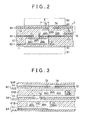
- FIG. 2 is a sectional view of the circuit board 5 at a portion including the U-phase direct-coupled FETs 21, 22.
- the FETs 21, 23, 25 are referred to as "upper-row FETs 20A", and the description of the upper-row FET 20A that is the U-phase direct-coupled FET 21 also applies to the description of the V-phase direct-coupled FET 23 and the description of the W-phase direct-coupled FET 25.
- the FETs 22, 24, 26 are referred to as "lower-row FETs 20B", and the description of the lower-row FET 20B that is the U-phase direct-coupled FET 22 also applies to the description of the V-phase direct-coupled FET 24 and the description of the W-phase direct-coupled FET 26.
- the circuit board 5 includes a multilayer printed wiring board 6, the upper-row FET 20A, the lower-row FET 20B, insulators 81, 82 and heat dissipation mechanisms 91, 92.
- the multilayer printed wiring board 6 includes an insulator 61, a plurality of conductor layers 62, 63, 64 and a plurality of vias 71, 72, 73, 74.
- the insulator 61 supports the conductor layers 62, 63, 64.
- the conductor layers 62, 63, 64 overlap with one another in the thickness direction of the multilayer printed wiring board 6.
- the laminated conductor layers 62, 63, 64 are function as conductor layers of internal layers arranged inside the insulator 61.
- the conductor layer 62 includes the drain line 11.
- the conductor layer 63 includes the upper-row gate line 12 and the serial line 13.
- the conductor layer 64 includes the lower-row gate line 14 and the source line 15.
- the vias 71, 72, 73, 74 function as interlayer connection members for connecting the layers.
- the via 71 connects the upper-row FET 20A and the upper-row gate line 12 of the conductor layer 63 to each other.
- the via 72 connects the upper-row FET 20A and the serial line 13 of the conductor layer 63 to each other.
- the via 73 connects the lower-row FET 20B and the lower-row gate line 14 of the conductor layer 64 to each other,
- the via 74 connects the lower-row FET 20B and the source line 15 of the conductor layer 64 to each other.
- the upper-row FET 20A and the lower-row FET 20B each are formed of a bare chip.
- the upper-row FET 20A and the lower-row FET 20B each have the gate terminal 20G and the source terminal 20S at one surface and the drain terminal 20D at the other surface.
- the laminated direction in which the conductor layers 62, 63, 64 are laminated that is, the thickness direction of the multilayer printed wiring board 6, the upper-row FET 20A and the lower-row FET 20B are arranged in overlapped position.
- the upper-row FET 20A is arranged on the conductor layer 62.
- the drain terminal 20D of the upper-row FET 20A is connected to the drain line 11 of the conductor layer 62.
- the gate terminal 20G of the upper-row FET 20A is connected to the upper-row gate line 12 of the conductor layer 63 through the via 71.
- the source terminal 20S of the upper-row FET 20A is connected to the conductor layer 63 that constitutes the serial line 13 through the via 72 that constitutes the serial line 13.
- the lower-row FET 20B is arranged on the conductor layer 63.
- the drain terminal 20D of the lower-row FET 20B is connected to the serial line 13 of the conductor layer 63.
- the gate terminal 20G of the lower-row FET 20B is connected to the lower-row gate line 14 of the conductor layer 64 through the via 73.
- the source terminal 20S of the lower-row FET 20B is connected to the conductor layer 64 that constitutes the source line 15 through the via 74 that constitutes the source line 15.
- the insulators 81, 82 prevent a short circuit in a circuit (not shown) on the surface of the multilayer printed wiring board 6.
- the insulators 81, 82 are, for example, formed of an electrically insulating material having a high coefficient of thermal conductivity, such as ceramics. Between both surfaces of the multilayer printed wiring board 6, the insulator 81 is arranged on a surface close to the upper-row FET 20A between the upper-row FET 20A and the lower-row FET 20B. Between both surfaces of the multilayer printed wiring board 6, the insulator 82 is arranged on a surface close to the lower-row FET 20B between the upper-row FET 20A and the lower-row FET 20B.
- the heat dissipation mechanisms 91, 92 dissipate heat that is generated from the upper-row FET 20A and the lower-row FET 20B.
- the heat dissipation mechanisms 91. 92 each are, for example, formed of a cooler, a heat sink, or the like.
- the heat dissipation mechanisms 91, 92 are arranged at locations at which the heat dissipation mechanisms 91, 92 overlap with the upper-row FET 20A and the lower-row FET 20B.
- thermoplastic resin sheet 61B As shown in FIG. 3 , a board 6A, a thermoplastic resin sheet 61B, the upper-row FET 20A, a board 6B, a thermoplastic resin sheet 61D, the lower-row FET 20B, a board 6C and a thermoplastic resin sheet 61F are prepared.
- the configuration of the prepared board 6A, thermoplastic resin sheet 61B, upper-row FET 20A, board 6B, thermoplastic resin sheet 61D, lower-row FET 20B, board 6C and thermoplastic resin sheet 61F will be described.
- the board 6A has a thermoplastic resin sheet 61A and the drain line 11.
- the drain line 11 is formed on the thermoplastic resin sheet 61A.
- the thermoplastic resin sheet 61B buries a gap between the board 6A and the board 6B when the board 6A and the board 6B are laminated via the upper-row FET 20A.
- the board 6B has a thermoplastic resin sheet 61C, the upper-row gate line 12, the serial line 13 and the vias 71, 72.
- the upper-row gate line 12 and the serial line 13 are formed on the thermoplastic resin sheet 61C.
- the vias 71, 72 extend through the thermoplastic resin sheet 61C.
- the via 71 has the upper-row gate line 12 as its bottom face
- the via 72 has the serial line 13 as its bottom face.
- the thermoplastic resin sheet 61D buries a gap between the board 6B and the board 6C when the board 6B and the board 6C are laminated via the lower-row FET 20B.
- the board 6C has a thermoplastic resin sheet 61E, the lower-row gate line 14, the source line 15 and the vias 73, 74.
- the lower-row gate line 14 and the source line 15 are formed on the thermoplastic resin sheet 61 E.
- the vias 73, 74 extend through the thermoplastic resin sheet 61E.
- the via 73 has the lower-row gate line 14 as its bottom face
- the via 74 has the source line 15 as its bottom face.
- the thermoplastic resin sheet 61F covers the lower-row gate line 14 and the source line 15 on the thermoplastic resin sheet 61E when the thermoplastic resin sheet 61F is laminated on the board 6C.
- thermoplastic resin sheet 61B The above-described board 6A, thermoplastic resin sheet 61B, upper-row FET 20A, board 6B, thermoplastic resin sheet 61D, lower-row FET 20B, board 6C and thermoplastic resin sheet 61F are laminated.
- the board 6A, the thermoplastic resin sheet 61B, the upper-row FET 20A, the board 6B, the thermoplastic resin sheet 61D, the lower-row FET 20B, the board 6C and the thermoplastic resin sheet 61F are pressed while being heated.
- the thermoplastic resin sheets 61A, 61B, 61C, 61D, 61E heated in this hot pressing process melt, and, after that, is cured by stop heating.
- the insulator 61 shown in FIG. 2 is formed from the cured thermoplastic resin sheets 61A, 61B, 61C, 61D, 61E.
- the circuit board 5 is obtained by arranging the heat dissipation mechanisms 91, 92 on the surfaces of the multilayer printed wiring board 6 via the insulators 81, 82.
- the circuit board 5 is mounted on the in-vehicle motor control device.
- Heat generated from the upper-row FET 20A is transferred to the heat dissipation mechanism 91 implemented on one surface of the multilayer printed wiring board 6, and heat generated from the lower-row FET 20B is transferred to the heat dissipation mechanism 92 implemented on the other surface of the multilayer printed wiring board 6.
- the circuit board 5 according to the present embodiment has the following advantageous effects. (1) In the laminated direction in which the conductor layers 62, 63, 64 are laminated, the U-phase direct-coupled FET 21 and the U-phase direct-coupled FET 22 overlap with each other. Therefore, in comparison with the case where the U-phase direct-coupled FET 21 and the U-phase direct-coupled FET 22 are arranged on the surface of the multilayer printed wiring board 6, it is possible to reduce the area of the multilayer printed wiring board 6.
- the V-phase direct-coupled FET 23 and the V-phase direct-coupled FET 24 overlap with each other. Therefore, in comparison with the case where the V-phase direct-coupled FET 23 and the V-phase direct-coupled FET 24 are arranged on the surface of the multilayer printed wiring board 6, it is possible to reduce the area of the multilayer printed wiring board 6.
- the W-phase direct-coupled FET 25 and the W-phase direct-coupled FET 26 overlap with each other. Therefore, in comparison with the case where the W-phase direct-coupled FET 25 and the W-phase direct-coupled FET 26 are arranged on the surface of the multilayer printed wiring board 6, it is possible to reduce the area of the multilayer printed wiring board 6.
- Both the V-phase direct-coupled FET 23 and the V-phase direct-coupled FET 24 are incorporated in the multilayer printed wiring board 6. Therefore, it is not required to arrange the V-phase direct-coupled FET 23 and the V-phase direct-coupled FET 24 on the surface of the multilayer printed wiring board 6. Thus, it is possible to further increase the flexibility of design and arrangement of the heat dissipation mechanisms 91, 92 that are arranged on the surfaces of the multilayer printed wiring board 6.
- Both the W-phase direct-coupled FET 25 and the W-phase direct-coupled FET 26 are incorporated in the multilayer printed wiring board 6. Therefore, it is not required to arrange the W-phase direct-coupled FET 25 and the W-phase direct-coupled FET 26 on the surface of the multilayer printed wiring board 6. Thus, it is possible to further increase the flexibility of design and arrangement of the heat dissipation mechanisms 91, 92 that are arranged on the surfaces of the multilayer printed wiring board 6.
- the U-phase direct-coupled FET 21 and the U-phase direct-coupled FET 22 overlap with each other in the above-described laminated direction, so the serial line 13U that serially connects the high potential-side switching element and the low potential-side switching element to each other can be, formed of a via, and it is possible to shorten the serial line 13U.
- the W-phase direct-coupled FET 25 and the W-phase direct-coupled FET 26 overlap with each other in the above-described laminated direction, so the serial line 13W that serially connects the high potential-side switching element and the low potential-side switching element to each other can be, formed of a via, and it is possible to shorten the serial line 13W.
- the source terminal 20S of the U-phase direct-coupled FET 21 is arranged at a location at which the source terminal 20S of the U-phase direct-coupled FET 21 overlaps with the drain terminal 20D of the U-phase direct-coupled FET 22 in the above-described laminated direction, so it is possible to reduce the distance from the source terminal 20S of the U-phase direct-coupled FET 21 to the drain terminal 20D of the U-phase direct-coupled FET 22. Thus, it is possible to further shorten the serial line 13U.
- the source terminal 20S of the V-phase direct-coupled FET 23 is arranged at a location at which the source terminal 20S of the V-phase direct-coupled FET 23 overlaps with the drain terminal 20D of the V-phase direct-coupled FET 24 in the above-described laminated direction, so it is possible to reduce the distance from the source terminal 20S of the V-phase direct-coupled FET 23 to the drain terminal 20D of the V-phase direct-coupled FET 24. Thus, it is possible to further shorten the serial line 13V.
- the source terminal 20S of the W-phase direct-coupled FET 25 is arranged at a location at which the source terminal 20S of the W-phase direct-coupled FET 25 overlaps with the drain terminal 20D of the W-phase direct-coupled FET 26 in the above-described laminated direction, so it is possible to reduce the distance from the source terminal 20S of the W-phase direct-coupled FET 25 to the drain terminal 20D of the W-phase direct-coupled FET 26. Thus, it is possible to further shorten the serial line 13W.
- the heat dissipation mechanisms 91, 92 are respectively arranged on both surfaces of the multilayer printed wiring board 6 via the insulators 81, 82. Therefore, in comparison with a configuration that a heat dissipation mechanism is arranged only on one surface of the multilayer printed wiring board 6, it is possible to improve the heat dissipation effect.
- the invention includes embodiments other than the above-described embodiment.
- alternative embodiments to the above-described embodiment will be described as other embodiments of the invention.
- the following alternative embodiments may be combined with each other.
- the FETs 21 to 26 are power MOSFETs. In contrast, in the circuit board 5. according to an alternative embodiment, the FETs 21 to 26 are junction FETs. In the circuit board 5 according to the embodiment, the upper-row FET 20A and the lower-row FET 20B overlap with each other. In contrast, in the circuit board 5 according to an alternative embodiment, for example, the U-phase direct-coupled FET 21 and the V-phase direct-coupled FET 23 are arranged in overlapped position. That is, the overlapped FETs 20 do not need to be serially connected to each other.
- both the upper-row FET 20A and the lower-row FET 20B are incorporated in the multilayer printed wiring board 6.
- any one of the upper-row FET 20A and the lower-row FET 20B is incorporated in the multilayer printed wiring board 6.
- both the upper-row FET 20A and the lower-row FET 20B are not incorporated in the multilayer printed wiring board 6 but are implemented on the surface of the multilayer printed wiring board 6.
- the heat dissipation mechanisms 91, 92 are respectively arranged on both surfaces of the multilayer printed wiring board 6.
- a heat dissipation mechanism is arranged on any one of the surfaces of the multilayer printed wiring board 6.
Landscapes
- Engineering & Computer Science (AREA)
- Manufacturing & Machinery (AREA)
- Microelectronics & Electronic Packaging (AREA)
- Power Engineering (AREA)
- Production Of Multi-Layered Print Wiring Board (AREA)
- Inverter Devices (AREA)
- Structure Of Printed Boards (AREA)
Abstract
Description
- The invention relates to a motor control multilayer circuit board that includes a multilayer printed wiring board, a first field-effect transistor, a second field-effect transistor and a heat dissipation mechanism.
- A low temperature co-fired ceramics (LTCC) multilayer board described in Japanese Patent Application Publication No.
2011-83063 JP 2011-83063 A - The motor control multilayer circuit board is, for example, mounted on an in-vehicle motor control device, and a small-area multilayer printed wiring board is desired in order to be arranged in limited space. However, when a plurality of field-effect transistors are implemented on the surface of a multilayer printed wiring board, it is required to ensure space for implementing the field-effect transistors, so it is difficult to reduce the area of the multilayer printed wiring board.
- The invention provides a motor control multilayer circuit board that allows a reduction in the area of a multilayer printed wiring board.
- An aspect of the invention provides a motor control multilayer circuit board. The motor control multilayer circuit board includes: a multilayer printed wiring board having a plurality of laminated conductor layers; a first field-effect transistor that is connected to the conductor layers and that controls a motor; a second field-effect transistor that is connected to the conductor layers, that is arranged at a location at which the second field-effect transistor overlaps with the first field-effect transistor in a laminated direction in which the conductor layers are laminated, and that controls the motor; and a heat dissipation mechanism arranged on the multilayer printed wiring board and arranged at a location at which the heat dissipation mechanism overlaps with at least one of the first field-effect transistor and the second field-effect transistor in the laminated direction.
- With the above motor control multilayer circuit board, the first field-effect transistor and the second field-effect transistor overlap with each other in the laminated direction in which the conductor layers are laminated. Therefore, in comparison with the case where the first field-effect transistor and the second field-effect transistor are arranged on the surface of the multilayer printed wiring board, it is possible to reduce the area of the multilayer printed wiring board. In addition, it is possible to dissipate heat generated from at least one of the first field-effect transistor and the second field-effect transistor with the use of the heat dissipation mechanism that overlaps with the at least one of the first field-effect transistor and the second field-effect transistor in the laminated direction.
- In the motor control multilayer circuit board according to the above aspect, at least one of the first field-effect transistor and the second field-effect transistor may be incorporated in the multilayer printed wiring board,
- With the above motor control multilayer circuit board, the multilayer printed wiring board incorporates at least one of the first field-effect transistor and the second field-effect transistor, so it is not required to arrange the at least one of the first field-effect transistor and the second field-effect transistor on the surface of the multilayer printed wiring board. Thus, it is possible to increase the flexibility of design and arrangement of the heat dissipation mechanism that is arranged on the surface of the multilayer printed wiring board.
- In the motor control multilayer circuit board according to the above aspect, both the first field-effect transistor and the second field-effect transistor may be incorporated in the multilayer printed wiring board.
- With the above motor control multilayer circuit board, the multilayer printed wiring board incorporates both the first field-effect transistor and the second field-effect transistor, so it is not required to arrange the first field-effect transistor and the second field-effect transistor on the surface of the multilayer printed wiring board. Thus, it is possible to increase the flexibility of design and arrangement of the heat dissipation mechanism that is arranged on the surface of the multilayer printed wiring board.
- In the motor control multilayer circuit board according to the above aspect, the first field-effect transistor and the second field-effect transistor may be serially connected to each other by a serial line, the first field-effect transistor may function as a switching element that is arranged on a higher potential side than the second field-effect transistor, and the second field-effect transistor may function as a switching element that is arranged on a lower potential side than the first field-effect transistor.
- With the above motor control multilayer circuit board, the first field-effect transistor and the second field-effect transistor overlap with each other in the laminated direction, so it is possible to shorten the serial line that serially connects the high potential-side switching element and the low potential-side switching element to each other.
- In the motor control multilayer circuit board according to the above aspect, the first field-effect transistor and the second field-effect transistor each may be a power MOSFET having a gate terminal and a source terminal at one surface and having a drain terminal at the other surface, and the source terminal of the first field-effect transistor may be arranged at a position at which the source terminal of the first field-effect transistor overlaps with the drain terminal of the second field-effect transistor in the laminated direction.
- With the above motor control multilayer circuit board, the source terminal of the first field-effect transistor is arranged at a location at which the source terminal of the first field-effect transistor overlaps with the drain terminal of the second field-effect transistor, so it is possible to reduce the distance from the source terminal of the first field-effect transistor to the drain terminal of the second field-effect transistor. Thus, it is possible to further shorten the serial line.
- In the motor control multilayer circuit board according to the above aspect, the heat dissipation mechanism may be arranged on each surface of the multilayer printed wiring board via an insulator.
- The above motor control multilayer circuit board includes the heat dissipation mechanism that is arranged on each surface of the multilayer printed wiring board via the insulator, so it is possible to improve the heat dissipation effect in comparison with the configuration that the heat dissipation mechanism is arranged only on one surface of the multilayer printed wiring board.
- According to the aspect of the invention, it is possible to provide the motor control multilayer circuit board that allows a reduction in the area of the multilayer printed wiring board.
- Features, advantages, and technical and industrial significance of exemplary embodiments of the invention will be described below with reference to the accompanying drawings, in which like numerals denote like elements, and wherein:
-
FIG. 1 is a configuration view that shows the overall configuration of a motor control device according to an embodiment of the invention; -
FIG. 2 is a sectional view that shows the sectional structure of a motor control multilayer circuit board according to the embodiment; and -
FIG. 3 is a sectional view that shows the sectional structure of each of printed wiring boards that constitute the motor control multilayer circuit board according to the embodiment. - An in-vehicle
motor control device 1 will be described with reference toFIG. 1 . Themotor control device 1 includes aninverter circuit 10, arotation angle sensor 30 and acontrol circuit 40. Themotor control device 1 drives amotor 3 using electric power from apower supply 2. - The
power supply 2 is, for example, formed of an in-vehicle battery or power generating device. Thepower supply 2 functions as a direct-current power supply. Thepower supply 2 supplies electric power to themotor 3 via theinverter circuit 10. - The
motor 3 is, for example, formed of an assist motor for an electric power steering system or an oil pump motor for an electric hydraulic power steering system. Themotor 3 includes astator 3A and arotor 3B. - The
stator 3A has aU-phase coil 3U, a V-phase coil 3V and a W-phase coil 3W. TheU-phase coil 3U, the V-phase coil 3V and the W-phase coil 3W are connected to one another by a Y connection collectively at a neutral point. - The
rotor 3B has N-poles and S-poles. The N-poles and the S-poles are located alternately in the rotation direction of therotor 3B. Therotor 3B rotates relative to thestator 3A due to revolving magnetic fields that are generated by thestator 3A. - The
inverter circuit 10 converts direct current, which is supplied from thepower supply 2, to three-phase alternating currents, and supplies the three-phase alternating currents to coils 3U, 3V, 3W of thestator 3A. Theinverter circuit 10 includes a plurality of field-effect transistors 20 (hereinafter, "FETs 20"),drain lines 11, upper-row gate lines 12,serial lines 13, lower-row gate lines 14 andsource lines 15. TheFETs 20 each are formed of a power metal-oxide-semiconductor field-effect transistor (MOSFET). - Each of the
FETs 20 has adrain terminal 20D that constitutes a drain, agate terminal 20G that constitutes a gate and asource terminal 20S that constitutes a source. In each MOSFET, the gate and the channel are electrically insulated from each other. The channel is a current path between the drain and the source. In each N-channel FET 20, thedrain terminal 20D is arranged on a higher potential side than thesource terminal 20S. - The
FETs 20 of theinverter circuit 10 include the two U-phase direct-coupledFETs FETs serial line 13U. The U-phase direct-coupledFET 21 functions as a switching element that is arranged on a higher potential side than the U-phase direct-coupledFET 22. Thus, the U-phase direct-coupledFET 22 functions as a switching element that is arranged on a lower potential side than the U-phase direct-coupledFET 21. - The
FETs 20 of theinverter circuit 10 include the two V-phase direct-coupledFETs FETs serial line 13V. The V-phase direct-coupledFET 23 functions as a switching element that is arranged on a higher potential side than the V-phase direct-coupledFET 24. Thus, the V-phase direct-coupledFET 24 functions as a switching element that is arranged on a lower potential side than the V-phase direct-coupledFET 23. - The
FETs 20 of theinverter circuit 10 include the two W-phase direct-coupledFETs 25. 26. The W-phase direct-coupledFETs serial line 13W. The W-phase direct-coupledFET 25 functions as a switching element that is arranged on a higher potential side than the W-phase direct-coupledFET 26. Thus, the W-phase direct-coupledFET 26 functions as a switching element that is arranged on a lower potential side than the W-phase direct-coupledFET 25. - The drain lines 11 connect the
power supply 2 to the U-phase direct-coupledFET 21, the V-phase direct-coupledFFT 23 and the W-phase direct-coupledFET 25. The drain lines 11 of theinverter circuit 10 include the drain line 11U for the U-phase direct-coupledFET 21, thedrain line 11V for the V-phase direct-coupledFET 23 and thedrain line 11W for the W-phase direct-coupledFET 25. - The upper-
row gate lines 12 connect thecontrol circuit 40 to the U-phase direct-coupledFET 21, the V-phase direct-coupledFET 23 and the W-phase direct-coupledFET 25. The upper-row gate lines 12 of theinverter circuit 10 include the upper-row gate line 12U for the U-phase direct-coupledFET 21, the upper-row gate line 12V for the V-phase direct-coupledFET 23 and the upper-row gate line 12W for the W-phase direct-coupledFET 25. - The
serial lines 13 connect theinverter circuit 10 to thecoils motor 3. Theserial lines 13 of theinverter circuit 10 include the U-phaseserial line 13U, the V-phaseserial line 13V and the W-phaseserial line 13W. - The lower-
row gate lines 14 connect thecontrol circuit 40 to the U-phase direct-coupledFET 22, the V-phase direct-coupledFET 24 and the W-phase direct-coupledFET 26. The lower-row gate lines 14 of theinverter circuit 10 include the lower-row gate line 14U for the U-phase direct-coupledFET 22, the lower-row gate line 14V for the V-phase direct-coupledFET 24 and the lower-row gate line 14W for the W-phase direct-coupledFET 26. - The source lines 15 connect the U-phase direct-coupled
FET 22, the V-phase direct-coupledFET 24 and the W-phase direct-coupledFET 26 to a reference potential point. The source lines 15 of theinverter circuit 10 include thesource line 15U for the U-phase direct-coupledFET 22, thesource line 15V for the V-phase direct-coupledFET 24 and thesource line 15W for the W-phase direct-coupledFET 26. - The configuration of connection of the
FETs 21 to 26 will be described in detail. Thedrain terminal 20D of the U-phase direct-coupledFET 21 is electrically connected to thepower supply 2 by the drain line 11U. Thegate terminal 20G of the U-phase direct-coupledFET 21 is electrically connected to thecontrol circuit 40 by the upper-row gate line 12U. Thesource terminal 20S of the U-phase direct-coupledFET 21 and thedrain terminal 20D of the U-phase direct-coupledFET 22 are electrically connected to each other by theserial line 13U. Thegate terminal 20G of the U-phase direct-coupledFET 22 is electrically connected to thecontrol circuit 40 by the lower-row gate line 14U. Thesource terminal 20S of the U-phase direct-coupledFET 22 is connected to the reference potential point by thesource line 15U. - The
serial line 13U is electrically connected to theU-phase coil 3U. Thus, theU-phase coil 3U of themotor 3 is electrically connected between the U-phase direct-coupledFETs inverter circuit 10. - The
drain terminal 20D of the V-phase direct-coupledFET 23 is electrically connected to thepower supply 2 by thedrain line 11V. Thegate terminal 20G of the V-phase direct-coupledFET 23 is electrically connected to thecontrol circuit 40 by the upper-row gate line 12V. Thesource terminal 20S of the V-phase direct-coupledFET 23 and thedrain terminal 20D of the V-phase direct-coupledFET 24 are electrically connected to each other by theserial line 13V. Thegate terminal 20G of the V-phase direct-coupledFET 24 is electrically connected to thecontrol circuit 40 by the lower-row gate line 14V. Thesource terminal 20S of the V-phase direct-coupledFET 24 is connected to the reference potential point by thesource line 15V. - The
serial line 13V is electrically connected to the V-phase coil 3V. Thus, the V-phase coil 3V of themotor 3 is electrically connected between the V-phase direct-coupledFETs inverter circuit 10. - The
drain terminal 20D of the W-phase direct-coupledFET 25 is electrically connected to thepower supply 2 by thedrain line 11W. Thegate terminal 20G of the W-phase direct-coupledFET 25 is electrically connected to thecontrol circuit 40 by the upper-row gate line 12W. Thesource terminal 20S of the W-phase direct-coupledFET 25 and thedrain terminal 20D of the W-phase direct-coupledFET 26 are electrically connected to each other by theserial line 13W. Thegate terminal 20G of the W-phase direct-coupledFET 26 is electrically connected to thecontrol circuit 40 by the lower-row gate line 14W. Thesource terminal 20S of the W-phase direct-coupledFET 26 is connected to the reference potential point by thesource line 15W. - The
serial line 13W is electrically connected to the W-phase coil 3W. Thus, the W-phase coil 3W of themotor 3 is electrically connected between the W-phase direct-coupledFETs inverter circuit 10. - The
rotation angle sensor 30 detects the rotation angle of themotor 3. Therotation angle sensor 30 outputs the detected rotation angle of themotor 3 to thecontrol circuit 40. Thecontrol circuit 40 controls theinverter circuit 10 by controlling switching operations of theFETs 21 to 26 on the basis of the detected rotation angle of themotor 3. - The operation of the
motor control device 1 will be described. Themotor control device 1 controls electric power, which is supplied to themotor 3, by controlling theinverter circuit 10 with the use of thecontrol circuit 40. As electric power is supplied to themotor 3, thestator 3A generates revolving magnetic fields, and therotor 3B rotates. Thecontrol circuit 40 executes feedback control over theinverter circuit 10 on the basis of the detected rotation angle of therotor 3B. - A motor control multilayer circuit board 5 (hereinafter, "
circuit board 5") that includes theinverter circuit 10 shown inFIG. 1 will be described with reference toFIG. 2. FIG. 2 is a sectional view of thecircuit board 5 at a portion including the U-phase direct-coupledFETs FET 25 shown inFIG. 1 are also arranged similarly to the U-phase direct-coupledFET 21 in thecircuit board 5, so theFETs row FETs 20A", and the description of the upper-row FET 20A that is the U-phase direct-coupledFET 21 also applies to the description of the V-phase direct-coupledFET 23 and the description of the W-phase direct-coupledFET 25. In addition, the V-phase direct-coupledFET 24 and the W-phase direct-coupledFET 26 shown inFIG. 1 are also arranged similarly to the U-phase direct-coupledFET 22 in thecircuit board 5, so theFETs row FETs 20B", and the description of the lower-row FET 20B that is the U-phase direct-coupledFET 22 also applies to the description of the V-phase direct-coupledFET 24 and the description of the W-phase direct-coupledFET 26. - The
circuit board 5 includes a multilayer printedwiring board 6, the upper-row FET 20A, the lower-row FET 20B,insulators heat dissipation mechanisms wiring board 6 includes aninsulator 61, a plurality of conductor layers 62, 63, 64 and a plurality ofvias - The
insulator 61 supports the conductor layers 62, 63, 64. The conductor layers 62, 63, 64 overlap with one another in the thickness direction of the multilayer printedwiring board 6. The laminated conductor layers 62, 63, 64 are function as conductor layers of internal layers arranged inside theinsulator 61. Theconductor layer 62 includes thedrain line 11. Theconductor layer 63 includes the upper-row gate line 12 and theserial line 13. The conductor layer 64 includes the lower-row gate line 14 and thesource line 15. - The
vias row FET 20A and the upper-row gate line 12 of theconductor layer 63 to each other. The via 72 connects the upper-row FET 20A and theserial line 13 of theconductor layer 63 to each other. The via 73 connects the lower-row FET 20B and the lower-row gate line 14 of the conductor layer 64 to each other, The via 74 connects the lower-row FET 20B and thesource line 15 of the conductor layer 64 to each other. - The upper-
row FET 20A and the lower-row FET 20B each are formed of a bare chip. The upper-row FET 20A and the lower-row FET 20B each have thegate terminal 20G and thesource terminal 20S at one surface and thedrain terminal 20D at the other surface. In the laminated direction in which the conductor layers 62, 63, 64 are laminated, that is, the thickness direction of the multilayer printedwiring board 6, the upper-row FET 20A and the lower-row FET 20B are arranged in overlapped position. - The upper-
row FET 20A is arranged on theconductor layer 62. Thedrain terminal 20D of the upper-row FET 20A is connected to thedrain line 11 of theconductor layer 62. Thegate terminal 20G of the upper-row FET 20A is connected to the upper-row gate line 12 of theconductor layer 63 through the via 71. Thesource terminal 20S of the upper-row FET 20A is connected to theconductor layer 63 that constitutes theserial line 13 through the via 72 that constitutes theserial line 13. - The lower-
row FET 20B is arranged on theconductor layer 63. Thedrain terminal 20D of the lower-row FET 20B is connected to theserial line 13 of theconductor layer 63. Thegate terminal 20G of the lower-row FET 20B is connected to the lower-row gate line 14 of the conductor layer 64 through the via 73. Thesource terminal 20S of the lower-row FET 20B is connected to the conductor layer 64 that constitutes thesource line 15 through the via 74 that constitutes thesource line 15. - The
insulators wiring board 6. Theinsulators wiring board 6, theinsulator 81 is arranged on a surface close to the upper-row FET 20A between the upper-row FET 20A and the lower-row FET 20B. Between both surfaces of the multilayer printedwiring board 6, theinsulator 82 is arranged on a surface close to the lower-row FET 20B between the upper-row FET 20A and the lower-row FET 20B. - The
heat dissipation mechanisms row FET 20A and the lower-row FET 20B. Theheat dissipation mechanisms 91. 92 each are, for example, formed of a cooler, a heat sink, or the like. In the laminated direction in which the conductor layers 62, 63, 64 are laminated, theheat dissipation mechanisms heat dissipation mechanisms row FET 20A and the lower-row FET 20B. - A manufacturing method for the
circuit board 5 will be described. As shown inFIG. 3 , a board 6A, athermoplastic resin sheet 61B, the upper-row FET 20A, aboard 6B, a thermoplastic resin sheet 61D, the lower-row FET 20B, a board 6C and athermoplastic resin sheet 61F are prepared. - The configuration of the prepared board 6A,
thermoplastic resin sheet 61B, upper-row FET 20A,board 6B, thermoplastic resin sheet 61D, lower-row FET 20B, board 6C andthermoplastic resin sheet 61F will be described. The board 6A has athermoplastic resin sheet 61A and thedrain line 11. Thedrain line 11 is formed on thethermoplastic resin sheet 61A. Thethermoplastic resin sheet 61B buries a gap between the board 6A and theboard 6B when the board 6A and theboard 6B are laminated via the upper-row FET 20A. Theboard 6B has athermoplastic resin sheet 61C, the upper-row gate line 12, theserial line 13 and thevias 71, 72. The upper-row gate line 12 and theserial line 13 are formed on thethermoplastic resin sheet 61C. Thevias 71, 72 extend through thethermoplastic resin sheet 61C. The via 71 has the upper-row gate line 12 as its bottom face, and the via 72 has theserial line 13 as its bottom face. The thermoplastic resin sheet 61D buries a gap between theboard 6B and the board 6C when theboard 6B and the board 6C are laminated via the lower-row FET 20B. The board 6C has a thermoplastic resin sheet 61E, the lower-row gate line 14, thesource line 15 and thevias row gate line 14 and thesource line 15 are formed on thethermoplastic resin sheet 61 E. The vias 73, 74 extend through the thermoplastic resin sheet 61E. The via 73 has the lower-row gate line 14 as its bottom face, and the via 74 has thesource line 15 as its bottom face. Thethermoplastic resin sheet 61F covers the lower-row gate line 14 and thesource line 15 on the thermoplastic resin sheet 61E when thethermoplastic resin sheet 61F is laminated on the board 6C. - The above-described board 6A,
thermoplastic resin sheet 61B, upper-row FET 20A,board 6B, thermoplastic resin sheet 61D, lower-row FET 20B, board 6C andthermoplastic resin sheet 61F are laminated. - The board 6A, the
thermoplastic resin sheet 61B, the upper-row FET 20A, theboard 6B, the thermoplastic resin sheet 61D, the lower-row FET 20B, the board 6C and thethermoplastic resin sheet 61F are pressed while being heated. Thus, the multilayer printedwiring board 6 is manufactured. Thethermoplastic resin sheets insulator 61 shown inFIG. 2 is formed from the curedthermoplastic resin sheets - After that, the
circuit board 5 is obtained by arranging theheat dissipation mechanisms wiring board 6 via theinsulators circuit board 5 is mounted on the in-vehicle motor control device. - The operation of the embodiment will be described. When the upper-
row FET 20A and the lower-row FET 20B are overlapped with each other, an overlapped portion X (seeFIG. 2 ) of the upper-row FET 20A and the lower-row FET 20B is formed in the multilayer printedwiring board 6. Therefore, it is possible to reduce the area of the overlapped portion X from the multilayer printed wiring board in which the upper-row FET 20A and the lower-row FET 20B are arranged on one surface. - Heat generated from the upper-
row FET 20A is transferred to theheat dissipation mechanism 91 implemented on one surface of the multilayer printedwiring board 6, and heat generated from the lower-row FET 20B is transferred to theheat dissipation mechanism 92 implemented on the other surface of the multilayer printedwiring board 6. - The
circuit board 5 according to the present embodiment has the following advantageous effects. (1) In the laminated direction in which the conductor layers 62, 63, 64 are laminated, the U-phase direct-coupledFET 21 and the U-phase direct-coupledFET 22 overlap with each other. Therefore, in comparison with the case where the U-phase direct-coupledFET 21 and the U-phase direct-coupledFET 22 are arranged on the surface of the multilayer printedwiring board 6, it is possible to reduce the area of the multilayer printedwiring board 6. In addition, it is possible to dissipate heat generated from the U-phrase direct-coupledFET 21 with the use of theheat dissipation mechanism 91 that overlaps with the U-phase direct-coupledFET 21 in the above laminated direction, and it is possible to dissipate heat generated from the U-phase direct-coupledFET 22 with the use of theheat dissipation mechanism 92 that overlaps with the U-phase direct-coupledFET 22 in the above laminated direction. - (2) In the laminated direction in which the conductor layers 62, 63, 64 are laminated, the V-phase direct-coupled
FET 23 and the V-phase direct-coupledFET 24 overlap with each other. Therefore, in comparison with the case where the V-phase direct-coupledFET 23 and the V-phase direct-coupledFET 24 are arranged on the surface of the multilayer printedwiring board 6, it is possible to reduce the area of the multilayer printedwiring board 6. In addition, it is possible to dissipate heat generated from the V-phase direct-coupledFET 23 with the use of theheat dissipation mechanism 91 that overlaps with the V-phase direct-coupledFET 23 in the above laminated direction, and it is possible to dissipate heat generated from the V-phase direct-coupledFET 24 with the use of theheat dissipation mechanism 92 that overlaps with the V-phase direct-coupledFET 24 in the above laminated direction. - (3) In the laminated direction in which the conductor layers 62, 63, 64 are laminated, the W-phase direct-coupled
FET 25 and the W-phase direct-coupledFET 26 overlap with each other. Therefore, in comparison with the case where the W-phase direct-coupledFET 25 and the W-phase direct-coupledFET 26 are arranged on the surface of the multilayer printedwiring board 6, it is possible to reduce the area of the multilayer printedwiring board 6. In addition, it is possible to dissipate heat generated from the W-phase direct-coupledFET 25 with the use of theheat dissipation mechanism 91 that overlaps with the W-phase direct-coupledFET 25 in the above laminated direction, and it is possible to dissipate heat generated from the W-phase direct-coupledFET 26 with the use of theheat dissipation mechanism 92 that overlaps with the W-phase direct-coupledFET 26 in the above laminated direction. - (4) Both the U-phase direct-coupled
FET 21 and the U-phrase direct-coupledFET 22 are incorporated in the multilayer printedwiring board 6. Therefore, it is not required to arrange the U-phase direct-coupledFET 21 and the U-phase direct-coupledFET 22 on the surface of the multilayer printedwiring board 6. Thus, it is possible to further increase the flexibility of design and arrangement of theheat dissipation mechanisms wiring board 6. - (5) Both the V-phase direct-coupled
FET 23 and the V-phase direct-coupledFET 24 are incorporated in the multilayer printedwiring board 6. Therefore, it is not required to arrange the V-phase direct-coupledFET 23 and the V-phase direct-coupledFET 24 on the surface of the multilayer printedwiring board 6. Thus, it is possible to further increase the flexibility of design and arrangement of theheat dissipation mechanisms wiring board 6. - (6) Both the W-phase direct-coupled
FET 25 and the W-phase direct-coupledFET 26 are incorporated in the multilayer printedwiring board 6. Therefore, it is not required to arrange the W-phase direct-coupledFET 25 and the W-phase direct-coupledFET 26 on the surface of the multilayer printedwiring board 6. Thus, it is possible to further increase the flexibility of design and arrangement of theheat dissipation mechanisms wiring board 6. - (7) The U-phase direct-coupled
FET 21 and the U-phase direct-coupledFET 22 overlap with each other in the above-described laminated direction, so theserial line 13U that serially connects the high potential-side switching element and the low potential-side switching element to each other can be, formed of a via, and it is possible to shorten theserial line 13U. - (8) The V-phsse direct-coupled
FET 23 and the V-phase direct-coupledFET 24 overlap with each other in the above-described laminated direction, so theserial line 13V that serially connects the high potential-side switching element and the low potential-side switching element to each other can be, formed of a via, and it is possible to shorten theserial line 13V. - (9) The W-phase direct-coupled
FET 25 and the W-phase direct-coupledFET 26 overlap with each other in the above-described laminated direction, so theserial line 13W that serially connects the high potential-side switching element and the low potential-side switching element to each other can be, formed of a via, and it is possible to shorten theserial line 13W. - (10) The
source terminal 20S of the U-phase direct-coupledFET 21 is arranged at a location at which thesource terminal 20S of the U-phase direct-coupledFET 21 overlaps with thedrain terminal 20D of the U-phase direct-coupledFET 22 in the above-described laminated direction, so it is possible to reduce the distance from thesource terminal 20S of the U-phase direct-coupledFET 21 to thedrain terminal 20D of the U-phase direct-coupledFET 22. Thus, it is possible to further shorten theserial line 13U. - (11) The
source terminal 20S of the V-phase direct-coupledFET 23 is arranged at a location at which thesource terminal 20S of the V-phase direct-coupledFET 23 overlaps with thedrain terminal 20D of the V-phase direct-coupledFET 24 in the above-described laminated direction, so it is possible to reduce the distance from thesource terminal 20S of the V-phase direct-coupledFET 23 to thedrain terminal 20D of the V-phase direct-coupledFET 24. Thus, it is possible to further shorten theserial line 13V. - (12) The
source terminal 20S of the W-phase direct-coupledFET 25 is arranged at a location at which thesource terminal 20S of the W-phase direct-coupledFET 25 overlaps with thedrain terminal 20D of the W-phase direct-coupledFET 26 in the above-described laminated direction, so it is possible to reduce the distance from thesource terminal 20S of the W-phase direct-coupledFET 25 to thedrain terminal 20D of the W-phase direct-coupledFET 26. Thus, it is possible to further shorten theserial line 13W. - (13) The
heat dissipation mechanisms wiring board 6 via theinsulators wiring board 6, it is possible to improve the heat dissipation effect. - The invention includes embodiments other than the above-described embodiment. Hereinafter, alternative embodiments to the above-described embodiment will be described as other embodiments of the invention. The following alternative embodiments may be combined with each other.
- In the
circuit board 5 according to the embodiment, theFETs 21 to 26 are power MOSFETs. In contrast, in thecircuit board 5. according to an alternative embodiment, theFETs 21 to 26 are junction FETs. In thecircuit board 5 according to the embodiment, the upper-row FET 20A and the lower-row FET 20B overlap with each other. In contrast, in thecircuit board 5 according to an alternative embodiment, for example, the U-phase direct-coupledFET 21 and the V-phase direct-coupledFET 23 are arranged in overlapped position. That is, the overlappedFETs 20 do not need to be serially connected to each other. - In the
circuit board 5 according to the embodiment, both the upper-row FET 20A and the lower-row FET 20B are incorporated in the multilayer printedwiring board 6. In contrast, in thecircuit board 5 according to an alternative embodiment, any one of the upper-row FET 20A and the lower-row FET 20B is incorporated in the multilayer printedwiring board 6. In addition, in thecircuit board 5 according to an alternative embodiment, both the upper-row FET 20A and the lower-row FET 20B are not incorporated in the multilayer printedwiring board 6 but are implemented on the surface of the multilayer printedwiring board 6. - In the
circuit board 5 according to the embodiment, theheat dissipation mechanisms wiring board 6. In contrast, in thecircuit board 5 according to an alternative embodiment, a heat dissipation mechanism is arranged on any one of the surfaces of the multilayer printedwiring board 6.
Claims (6)
- A motor control multilayer circuit board (5) characterized by comprising:a multilayer printed wiring board (6) having a plurality of laminated conductor layers (62,63,64);a first field-effect transistor (20A) that is connected to the conductor layers (62, 63) and that controls a motor (3);a second field-effect transistor (20B) that is connected to the conductor layers (63, 64), that is arranged at a location at which the second field-effect transistor overlaps with the first field-effect transistor in a laminated direction in which the conductor layers are laminated, and that controls the motor; anda heat dissipation mechanism (91, 92) arranged on the multilayer printed wiring board and arranged at a location at which the heat dissipation mechanism overlaps with at least one of the first field-effect transistor and the second field-effect transistor in the laminated direction.
- The motor control multilayer circuit board according to claim 1, wherein
at least one of the first field-effect transistor and the second field-effect transistor is incorporated in the multilayer printed wiring board. - The motor control multilayer circuit board according to claim 1 or 2, wherein
both the first field-effect transistor and the second field-effect transistor are incorporated in the multilayer printed wiring board. - The motor control multilayer circuit board according to any one of claims 1 to 3, wherein
the first field-effect transistor and the second field-effect transistor are serially connected to each other by a serial line (13),
the first field-effect transistor functions as a switching element that is arranged on a higher potential side than the second field-effect transistor, and
the second field-effect transistor functions as a switching element that is arranged on a lower potential side than the first field-effect transistor. - The motor control multilayer circuit board according to claim 4, wherein
the first field-effect transistor and the second field-effect transistor each are a power MOSFET having a gate terminal (20G) and a source terminal (20S) at one surface and having a drain terminal (20D) at the other surface, and
the source terminal of the first field-effect transistor is arranged at a position at which the source terminal of the first field-effect transistor overlaps with the drain terminal of the second field-effect transistor in the laminated direction. - The motor control multilayer circuit board according to any one of claims 1 to 5, wherein
the heat dissipation mechanism is arranged on each surface of the multilayer printed wiring board via an insulator (81, 82).
Applications Claiming Priority (1)
| Application Number | Priority Date | Filing Date | Title |
|---|---|---|---|
| JP2012097910A JP2013225622A (en) | 2012-04-23 | 2012-04-23 | Multilayer circuit board for motor control |
Publications (2)
| Publication Number | Publication Date |
|---|---|
| EP2658113A2 true EP2658113A2 (en) | 2013-10-30 |
| EP2658113A3 EP2658113A3 (en) | 2015-01-07 |
Family
ID=48182749
Family Applications (1)
| Application Number | Title | Priority Date | Filing Date |
|---|---|---|---|
| EP13164682.0A Withdrawn EP2658113A3 (en) | 2012-04-23 | 2013-04-22 | Motor control multilayer circuit board |
Country Status (4)
| Country | Link |
|---|---|
| US (1) | US8994120B2 (en) |
| EP (1) | EP2658113A3 (en) |
| JP (1) | JP2013225622A (en) |
| CN (1) | CN103379730A (en) |
Cited By (1)
| Publication number | Priority date | Publication date | Assignee | Title |
|---|---|---|---|---|
| WO2023179845A1 (en) * | 2022-03-22 | 2023-09-28 | Huawei Digital Power Technologies Co., Ltd. | Semiconductor power entity and method for producing such entity by hybrid bonding |
Families Citing this family (5)
| Publication number | Priority date | Publication date | Assignee | Title |
|---|---|---|---|---|
| JP6271265B2 (en) * | 2014-01-24 | 2018-01-31 | 日本電産サンキョー株式会社 | Motor drive device |
| CN104392980B (en) * | 2014-11-27 | 2019-02-15 | 深圳先进技术研究院 | A chip packaging structure |
| CN105576997B (en) * | 2016-02-04 | 2019-06-07 | 中国第一汽车股份有限公司 | A kind of inverter assembly of automobile-used integrated motor |
| CN114915270B (en) * | 2021-02-09 | 2025-11-21 | 开元通信技术(厦门)有限公司 | Radio frequency power amplifier and electronic equipment |
| WO2025248992A1 (en) * | 2024-05-30 | 2025-12-04 | 株式会社アイシン | Built-in substrate |
Citations (1)
| Publication number | Priority date | Publication date | Assignee | Title |
|---|---|---|---|---|
| JP2011083063A (en) | 2009-10-02 | 2011-04-21 | Mitsuba Corp | Drive controller and motor unit |
Family Cites Families (12)
| Publication number | Priority date | Publication date | Assignee | Title |
|---|---|---|---|---|
| JP4039202B2 (en) * | 2002-10-16 | 2008-01-30 | 日産自動車株式会社 | Stacked semiconductor device and assembly method thereof |
| US20050207133A1 (en) * | 2004-03-11 | 2005-09-22 | Mark Pavier | Embedded power management control circuit |
| JP4283753B2 (en) * | 2004-10-26 | 2009-06-24 | パナソニックエレクトロニックデバイス山梨株式会社 | Multi-layer printed wiring board with built-in electrical components and method for manufacturing the same |
| JP2006165175A (en) * | 2004-12-06 | 2006-06-22 | Alps Electric Co Ltd | Circuit component module, electronic circuit device, and circuit component module manufacturing method |
| CN100459083C (en) * | 2006-03-15 | 2009-02-04 | 日月光半导体制造股份有限公司 | Method for manufacturing substrate with embedded element |
| DE102007036045A1 (en) | 2007-08-01 | 2009-02-05 | Siemens Ag | Electronic component with at least one component, in particular a semiconductor component, and method for its production |
| US9147649B2 (en) | 2008-01-24 | 2015-09-29 | Infineon Technologies Ag | Multi-chip module |
| DE102008040906A1 (en) | 2008-07-31 | 2010-02-04 | Robert Bosch Gmbh | Printed circuit board with electronic component |
| US8120158B2 (en) | 2009-11-10 | 2012-02-21 | Infineon Technologies Ag | Laminate electronic device |
| WO2011083578A1 (en) | 2010-01-08 | 2011-07-14 | トヨタ自動車株式会社 | Semiconductor module |
| JP5273095B2 (en) * | 2010-05-24 | 2013-08-28 | 株式会社デンソー | Semiconductor device |
| JP2012009828A (en) | 2010-05-26 | 2012-01-12 | Jtekt Corp | Multilayer circuit board |
-
2012
- 2012-04-23 JP JP2012097910A patent/JP2013225622A/en active Pending
-
2013
- 2013-04-19 US US13/866,422 patent/US8994120B2/en not_active Expired - Fee Related
- 2013-04-22 EP EP13164682.0A patent/EP2658113A3/en not_active Withdrawn
- 2013-04-23 CN CN2013101431645A patent/CN103379730A/en active Pending
Patent Citations (1)
| Publication number | Priority date | Publication date | Assignee | Title |
|---|---|---|---|---|
| JP2011083063A (en) | 2009-10-02 | 2011-04-21 | Mitsuba Corp | Drive controller and motor unit |
Cited By (1)
| Publication number | Priority date | Publication date | Assignee | Title |
|---|---|---|---|---|
| WO2023179845A1 (en) * | 2022-03-22 | 2023-09-28 | Huawei Digital Power Technologies Co., Ltd. | Semiconductor power entity and method for producing such entity by hybrid bonding |
Also Published As
| Publication number | Publication date |
|---|---|
| JP2013225622A (en) | 2013-10-31 |
| EP2658113A3 (en) | 2015-01-07 |
| US8994120B2 (en) | 2015-03-31 |
| CN103379730A (en) | 2013-10-30 |
| US20130277761A1 (en) | 2013-10-24 |
Similar Documents
| Publication | Publication Date | Title |
|---|---|---|
| CN106856667B (en) | Electric motor driven power steering motor drive control device | |
| US8288658B2 (en) | Multilayer circuit board and motor drive circuit board | |
| US8994120B2 (en) | Motor control multilayer circuit board | |
| US7869193B2 (en) | Power conversion apparatus | |
| US9000633B2 (en) | Drive apparatus having a motor, a heat sink, and a plurality of semiconductor modules | |
| JP5967071B2 (en) | Electronic control device and electric power steering device using the same | |
| JP6444495B2 (en) | Electric power steering drive device | |
| JP5267959B2 (en) | Semiconductor module and driving device using the same | |
| JP5397417B2 (en) | Semiconductor device and driving device using the same | |
| US9978670B2 (en) | Semiconductor module and semiconductor driving device | |
| WO2010150528A1 (en) | Drive device | |
| WO2010150530A1 (en) | Drive device | |
| US10096572B2 (en) | Power semiconductor module and electric power steering apparatus using the same | |
| CN101006633B (en) | Rotating electric machine | |
| CN105406652A (en) | Power Conversion Device | |
| JP6020379B2 (en) | Semiconductor device | |
| CN104052308B (en) | Driving circuit device | |
| CN117121366A (en) | Multilayer circuit board, drive control device, and motor unit for electric power steering |
Legal Events
| Date | Code | Title | Description |
|---|---|---|---|
| PUAI | Public reference made under article 153(3) epc to a published international application that has entered the european phase |
Free format text: ORIGINAL CODE: 0009012 |
|
| AK | Designated contracting states |
Kind code of ref document: A2 Designated state(s): AL AT BE BG CH CY CZ DE DK EE ES FI FR GB GR HR HU IE IS IT LI LT LU LV MC MK MT NL NO PL PT RO RS SE SI SK SM TR |
|
| AX | Request for extension of the european patent |
Extension state: BA ME |
|
| PUAL | Search report despatched |
Free format text: ORIGINAL CODE: 0009013 |
|
| AK | Designated contracting states |
Kind code of ref document: A3 Designated state(s): AL AT BE BG CH CY CZ DE DK EE ES FI FR GB GR HR HU IE IS IT LI LT LU LV MC MK MT NL NO PL PT RO RS SE SI SK SM TR |
|
| AX | Request for extension of the european patent |
Extension state: BA ME |
|
| RIC1 | Information provided on ipc code assigned before grant |
Ipc: H05K 1/02 20060101ALI20141128BHEP Ipc: H02P 6/08 20060101AFI20141128BHEP Ipc: H05K 1/18 20060101ALI20141128BHEP Ipc: H05K 3/46 20060101ALI20141128BHEP |
|
| 17P | Request for examination filed |
Effective date: 20150707 |
|
| RBV | Designated contracting states (corrected) |
Designated state(s): AL AT BE BG CH CY CZ DE DK EE ES FI FR GB GR HR HU IE IS IT LI LT LU LV MC MK MT NL NO PL PT RO RS SE SI SK SM TR |
|
| STAA | Information on the status of an ep patent application or granted ep patent |
Free format text: STATUS: THE APPLICATION HAS BEEN WITHDRAWN |
|
| 18W | Application withdrawn |
Effective date: 20170628 |