EP2656433B1 - Achtförmiges balun - Google Patents
Achtförmiges balun Download PDFInfo
- Publication number
- EP2656433B1 EP2656433B1 EP11822901.2A EP11822901A EP2656433B1 EP 2656433 B1 EP2656433 B1 EP 2656433B1 EP 11822901 A EP11822901 A EP 11822901A EP 2656433 B1 EP2656433 B1 EP 2656433B1
- Authority
- EP
- European Patent Office
- Prior art keywords
- balun
- loop portion
- loop
- wound conductors
- wound
- Prior art date
- Legal status (The legal status is an assumption and is not a legal conclusion. Google has not performed a legal analysis and makes no representation as to the accuracy of the status listed.)
- Active
Links
Images





Classifications
-
- H—ELECTRICITY
- H03—ELECTRONIC CIRCUITRY
- H03H—IMPEDANCE NETWORKS, e.g. RESONANT CIRCUITS; RESONATORS
- H03H7/00—Multiple-port networks comprising only passive electrical elements as network components
- H03H7/42—Networks for transforming balanced signals into unbalanced signals and vice versa, e.g. baluns
-
- H—ELECTRICITY
- H01—ELECTRIC ELEMENTS
- H01P—WAVEGUIDES; RESONATORS, LINES, OR OTHER DEVICES OF THE WAVEGUIDE TYPE
- H01P5/00—Coupling devices of the waveguide type
- H01P5/08—Coupling devices of the waveguide type for linking dissimilar lines or devices
- H01P5/10—Coupling devices of the waveguide type for linking dissimilar lines or devices for coupling balanced lines or devices with unbalanced lines or devices
-
- H—ELECTRICITY
- H01—ELECTRIC ELEMENTS
- H01Q—ANTENNAS, i.e. RADIO AERIALS
- H01Q1/00—Details of, or arrangements associated with, antennas
- H01Q1/50—Structural association of antennas with earthing switches, lead-in devices or lightning protectors
Definitions
- Baluns are electrical transformers that convert electrical signals that are balanced about ground to electrical signals that are unbalanced about ground. Baluns may also convert electrical signals that are unbalanced about ground and convert the electrical signals to being balanced about ground.
- a balun typically includes two inductors where each inductor is formed from a set of wound conductors.
- the sets of wound conductors are inductively coupled if current is passed through one set of wound conductors.
- FIG. 1 is a simplified schematic of a traditional balun 100.
- Balun 100 includes a first set of wound conductors 105 and a second set of wound conductors 110.
- One wound conductor from each set of wound conductors 105 and 110 is shown in FIG. 1 for simplification.
- Each wound conductor in the set of wound conductors 105 may be adjacent to a wound conductor in the set of wound conductors 110.
- Traditional baluns typically tend to introduce a relatively large amount of cross talk (i.e., interference) with nearby circuits, such as other inductors, other baluns, and the like.
- WO 2009/144211 A1 relates to a radio frequency eight-shaped balun.
- This document discloses symmetrical eight-shaped balun (BALanced-to-UNbalanced converter) comprising a first and second eye, each eye comprising conducting tracks forming turns.
- the eyes comprise an equal number of primary turns which form a first conducting path from a first terminal to a second terminal, in which in operation an electrical current flows in a first direction in a first eye and in a second direction in a second eye.
- the eyes further comprise an equal number of secondary turns which form a second conducting path from a third terminal to a fourth terminal, in which in operation an electrical current flows in a first direction in a first eye and in a second direction in a second eye.
- the geometrical and electrical middle points of primary and secondary turns are all superposed and further are located in the same plane.
- FR 2 862 158 relates to a distributed balun with a non-unity impedance ration.
- US 2004/182602 A1 relates to a high frequency electronic circuit component. This document aims at miniaturizing a balance-unbalance converter using the conventional connection lines and reducing the cost thereof.
- Embodiments described herein generally relate to baluns, and more particularly relate to a balun having a figure 8 shape, which provide for equivalent power transfer compared to a traditional balun and provides such power transfer in relatively less area than a traditional balun.
- the first set of wound conductors includes a set of conductive cross portions disposed between the first loop portion and the second loop portion and conductively links the first loop portion and the second loop portion.
- the second set of wound conductors includes another set of conductive cross portions disposed between the third loop portion and the fourth loop portion and conductively links the third loop portion and the fourth loop portion.
- the first set of wound conductors includes a set of conductive un-crossing portions disposed between the first loop portion and the second loop portion and conductively links the first loop portion and the second loop portion.
- the second set of wound conductors includes another set of conductive un-crossing portions disposed between the third loop portion and the fourth loop portion and conductively links the third loop portion and the fourth loop portion.
- the first set of wound conductors are stacked above the second set of wound conductors.
- the wound conductors of the first set of wound conductors are interleaved with the wound conductors of the second set of wound conductors.
- the wound conductors of the first set of wound conductors are stacked and interleaved with the wound conductors of the second set of wound conductors.
- a number of wound conductors in the first set of wound conductors does not match a number of wound conductors in the second set of wound conductors.
- the balun further includes another balun disposed in the second and the fourth loop portions.
- the first, the second, the third, and the fourth loop portions are substantially round.
- the first, the second, the third, and the fourth loop portions are substantially oval.
- the first, the second, the third, and the fourth loop portions are substantially rectangular.
- the first, the second, the third, and the fourth loop portions each include substantially linear portions.
- Embodiments described herein generally provide to baluns, and more particularly provide a balun having a figure 8 shape, which provide for equivalent power transfer compared to a traditional balun and provides such power transfer in relatively less area than a traditional balun.
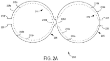
- FIG. 2A is a simplified schematic of a balun 200 according to one example.
- Balun 200 includes a first set of wound conductors 205 and a second set of wound conductors 210.
- one wound conductor 205a (shown as a solid line in FIG. 2A ) from the first set of wound conductors 205 is shown in FIG. 2A
- one wound conductor 210a (shown as a dashed line in FIG. 2A ) from the second set of wound conductors 210 is shown in FIG. 2A .
- the first set of wound conductors 205 may include an input node 215 and an output node 220.
- the second set of wound conductors 210 may include an input node 225 and an output node 230.
- balun 200 describes wound conductor 205a included in the set of wound conductors 205 and describes wound conductor 210a included in the set of wound conductors 210.
- wound conductor 205a and wound conductor 210a may apply to each of the wound conductors included the sets of wound conductors 205 and 210.
- wound conductor 205a may include a first loop 205b conductively coupled to a second loop 205c where the first loop 205b and the second loop 205c are adjacent.
- First loop 205b and second loop 205c may cross over each other in a central portion 205d of wound conductor 205a.
- first loop 205b and second loop 205c may form substantially a "figure eight" structure.
- Wound conductor 210a may similarly include a first loop 210b conductively coupled to a second loop 210c.
- First loop 210b and second loop 210c may cross over each other in a central portion 210d of wound conductor 210a.
- first loop 210b and second loop 210c may form substantially a "figure eight" structure.
- the central portions 205d and 210d may be laterally offset so that the crossing portions of the wound conductor 205a and 210a shown in FIG. 2A may cross at different locations.
- the crossing portions of the wound conductor 205a and 210a may be stacked or interleaved according to alternative embodiments.
- the centrals portion 205d of the first loop 205b and second loop 205c do not cross, and the central portion 210d of the first loop 210b and the second loop 210c do not cross.
- first loop 205b is shown in FIG. 2A as being outside of first loop 210b
- second loop 205c is shown as being outside of second loop 210c.
- the first loops 205b and 210b, and the second loops 205c and 210c may be alternatively configured with first loop 205b overlying first loop 210b and second loop 205c overlying second loop 210c.
- the set of wound conductors 205 are stacked above the set of wound conductors 210. Stacked sets of wound conductors 205 and 210 provide relatively low insertion loss and relatively high inductive coupling.
- the wound conductors of the set of wound conductors 205 and the wound conductors of the set of wound conductors 210 interleave one another. Interleaved wound conductors provide relatively low secondary resonances due to the capacitance provided by the parasitic capacitance between the sets of wound conductors.. Secondary resonances are lower order harmonics and higher order harmonics of the fundamental harmonic (i.e., fundamental frequency) of an AC signal received by balun 200.
- Stacked sets of wound conductors 205 and 210 may have relatively higher secondary resonances across cross capacitor 260 at relatively high frequencies.
- the sets of wound conductors 205 and 210 are both stacked and interleaved. Stacking and interleaving the sets of wound conductors 205 and 210 provides for a tradeoff between insertion losses and the generation of secondary resonances.
- FIG. 2B is a simplified schematic of magnetic fields established by first loop 205b and second loop 205c wherein the magnetic fields in the first and the second loops 205b and 205c are in opposite direction.
- the first and the second loops 210b and 210c are not shown in FIG. 2B for convenience.
- the direction of the magnetic field in first loop 205b may be out of the plane of the page of FIG. 2B (conventionally designated with a dot inside a circle " ⁇ " as shown in FIG. 2B ), and the direction of the magnetic field in second loop 205c may be into the plane of the page of FIG.
- first loops 205a and 210a will also be in the opposite direction of magnetic fields extending outside of second loops 205b and 210b. Because the magnetic fields established by first loop 205b is oppositely directed from the magnetic fields established by second loop 205c, the magnetic fields extending from balun 200 tend to cancel each other. The cancellation of the oppositely directed magnetic fields provides that the magnetic fields have a relatively reduced potential for inducing cross talk (i.e., interference) in adjacent circuits structures, such as inductors, other balun, and the like.
- inducing cross talk i.e., interference
- balun 200 may provide a gain of approximately 30dB of isolation from an adjacent circuit structure, such as another balun. While FIG. 2B shows the magnetic fields for the first loop 205b and the second loop 205c, the magnetic fields for first loop 210b and the second loop 210c are similar, but oppositely directed for the direction of current flow as shown in FIG. 2B .
- Balun 200 further provides an inductance that matches the inductance of a traditional balun while having a smaller area.
- balun 200 may provide an inductance that substantially matches the inductance of a traditional balun while having an area that is approximately 1.6 times to 1.7 times less than the area of a traditional balun. Therefore, for an application such as an integrated circuit, balun 200 may consume considerably less die area than a traditional balun.
- FIG. 3A is a simplified schematic of a balun 250 according to an alternative example where first loops 205b and 210b, and second loops 205c and 210c are substantially oval.
- FIG. 3B is a simplified schematic of a balun 260 according to an alternative example where first loops 205b and 210b, and second loops 205c and 210c are substantially oval. It is noted that the elongated axes of the oval shaped loops shown in FIG.
- FIG. 3A are rotated approximately ninety degrees from the elongated axes of the oval shaped loops shown in FIG. 3B.
- FIG. 3C is a simplified schematic of a balun 270 according to another alternative example where first loops 205b and 210b, and second loops 205c and 210c have substantially straight lines portions 280 and 285 along an extended axis 290 of balun 270. While balun 200 is described as including sets of wound conductors 205 and 210 in a figure 8, alternative balun examples may include more sets of wound conductors coupled to the set of wound conductors 205 or the set of wound conductors 210. Such a balun may look like three, four, or more sets of adjacent wound-conductor loops that are conductive coupled.
- the number of wound conductors in the first set of wound conductors 205 may match the number of wound conductors in the second set of wound conductors 210.
- the number of wound conductors in the first set of wound conductors 205 may be different than the number of wound conductors in the second set of wound conductors 210.
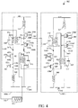
- FIG. 4 is a simplified schematic of a fully-differential power amplifier 500 inductively coupled to a coupler 505, which includes a set of inductors 515. Coupled 505 may be configured to inductively coupled the output of the fully-differential power amplifier 500 to an antenna 510. Balun embodiments described herein may be configured for inclusion in coupler 505 and first-fully differential amplifier 500 for inductively coupling coupler 505 to fully-differential power amplifier 500 as will be described in further detail below.
- Power amplifiers, such as fully-differential power amplifier 500 are generally configured to receive an AC signal, such as an RF signal, and boost the power of the received AC signal.
- Fully-differential power amplifiers may be included in a variety of mobile devices, such as mobile telephones, computers (such as laptop computers, tablet computers, etc.), personal digital assistants, and the like.
- a power-amplified AC signal may be directed through an antenna of a mobile device for transmission.
- Fully-differential power amplifier 500 includes a first power-amplifier core 300a (generally surrounded by a dashed line in FIG. 4 ) and a second power-amplifier core 300b (also generally surrounded by a dashed line in FIG. 4 ).
- the same numbering system used for identifying circuit elements of first power-amplifier core 300a is used for identifying the substantially same circuit elements of second power-amplifier core 300b where numbers used for second power-amplifier 300b are primed.
- the first and second power-amplifier cores 300a and 300b have substantially similar circuits and have substantially similar circuit layouts. Therefore, the first power-amplifier core 300a is described in detail, and the second power-amplifier core 300b is not described.
- the description of the first power-amplifier core 300a applies the second power-amplifier core 300b.
- First power-amplifier core 300a includes a push-pull pair of transistors 305 and 310, (referred to as transistors 305 and 310).
- First power-amplifier core 300a further includes a transistor 405 disposed between transistor 305 and a first inductor 315, and includes a transistor 410 disposed between transistor 310 and a second inductor 320.
- Transistors 405 and 410 are sometimes referred to herein as a second push-pull pair of transistors.
- Transistors 305 and 405 may be in a cascode configuration with a, respective, common source, common ground configuration. More specifically a source 405b of transistor 405 may be coupled to the drain 305c of transistor 305, and a drain 405c of transistor 405 may be coupled to the first end of first inductor 315 where the second end of first inductor 315 is coupled to the voltage source Vdd. A gate 405a of transistor 405 may be grounded or the like to relatively strongly turn on transistor 405.
- Transistors 310 and 410 may similarly be in a cascode configuration with a, respective, common source, common ground configuration. More specifically a source 410b of transistor 410 may be coupled to the drain 310b of transistor 310, and a drain 410c of transistor 410 may be coupled to the first end of second inductor 320 where the second end of inductor 320 is coupled to ground. A gate 410a of transistor 410 may be grounded or the like to relatively strongly turn on transistor 410.
- the cascode configuration of the transistors provide for stress protection of power amplifier 400 as will be well understood by those of skill in the art. According to one example, the gates 305a and 310a are first and second inputs 350 and 355 of fully-differential power amplifier 500.
- First power-amplifier core 300a may also include first and second tank capacitors 330 and 335.
- Capacitor 330 is coupled to inductor 315 in parallel (i.e., in a "tank" configuration).
- Tank capacitor 330 is configured to tune the resonant frequency of inductor 315.
- Tank capacitor 335 is coupled to inductor 320 in a tank configuration.
- Tank capacitor 335 is configured to tune the resonant frequency of inductor 320.
- Transistors 305, 310, 405, and 310 may be metal-oxide-semiconductor field-effect transistors (MOSFETs), bipolar-junction transistors (BJTs), or other transistors types.
- transistors 305 and 405 are nMOS transistors where transistor 405 has a drain 405c (sometimes referred to a drain region) coupled to a first end of inductor 315 where a second end of inductor 315 is coupled to a voltage source Vdd.
- a first output node (Vout1) 347a is disposed between drain 405c and the first end of inductor 315.
- a source 305b of transistor 305 may be coupled to a first end of a third inductor 340 where a second end of the third inductor 340 is coupled to ground.
- Specific configurations of the sources and the drains of transistors 305, 310, 405, and 410 are described herein for convenience of explanation of specific examples.
- Alternative examples of the power amplifiers may include alternative configurations of the sources and drains of transistors 305 and 310 as will be understood by those of skill in the art.
- sources and drains are sometimes referred to herein as source-drain nodes.
- transistors 310 and 410 are pMOS transistors where transistor 410 includes a drain 410c coupled a first end of inductor 320 where a second end of inductor 320 is coupled to ground.
- a second output node (Vout2) 347b is disposed between source 410c and the first end of inductor 320.
- a source 310c of transistor 310 is coupled a first end of a fourth inductor 345 where a second end of fourth inductor 345 is coupled to the voltage source Vdd.
- Inductors 315 and 320 may be considered the respective loads of the push-pull pair of transistors 305 and 310.
- coupler 505 via the set of inductors 515, is configured to inductively couple an output AC signals across inductors 315, 320, 315', and 320' to antenna 510.
- coupler 505 is shown as including the set of inductors 515 as a simplification for indicating the inductive coupling of the output AC signal across inductors 315, 320, 315', and 320' to antenna 510.
- balun examples described herein may be configured to inductively couple the AC output signals across inductors 315, 320, 315', and 320' to antenna 510.
- FIG. 5 is a simplified schematic of a balun 600 configured to inductively couple the output AC signals of fully-differential power amplifier 500 to antenna 510 according to one example.
- Balun 600 includes the first set of wound conductors 205 where the first loop 205b is inductively coupled to inductors 315 and 320, and the second loop 205c is inductively coupled to inductors 315' and 320'.
- Inductors 315 and 320 may be curved to conform to the loop shape of the first loop 205b, and inductors 315' and 320' may be curved to conform to a looped shape of the second loop 205c such that inductors 315 and 320, 315', and 320' form a substantially figure eight shape similar to the figure eight shape of the first set of wound conductors 205.
- Balun 600 may include inductors 315, 320, 315', and 320'.
- the first set of wound conductors 205 may inductively coupled the AC output signal across inductors 315, 320, 315', and 320' to antenna 510 for transmission of the AC output signal.
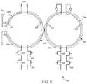
- inductors 315, 320, 315', and 320' may be shaped to substantially surround portions of the first loop 205b and the second loop 205c.
- FIG. 6 is a simplified schematic of balun 700 where inductors 315, 320, 315', and 320' substantially surround portions of the first loop 205b and the second loop 205c.
- FIG. 7 is a simplified schematic of balun 800 according to another example.
- Balun 800 is substantially similar to balun 600 and balun 700 described above, but differs in that balun 800 includes an additional first balun 200a and/or an additional second balun 200b where baluns 200a and 200b may be disposed in the first loop 205b and the second loop 205c.
- "Nesting" balun according to embodiments of the present invention may efficiently use space for these balun in an integrated circuit or the like.
- Balun 200a and 200b may each be a balun 200 described above or may be other balun examples described herein.
- Balun 200a and 200b may be configured for inductively coupling other circuit structures, such as a set of input inductors of fully-differential power amplifier 500. While inductors 315' and 320' are shown in FIGs. 5 , 6 , and 7 as being coupled to ground, according to alternative examples, inductors 315' and 320' may be coupled to an AC ground.
Landscapes
- Coils Or Transformers For Communication (AREA)
Claims (11)
- Balun (200), umfassend:einen ersten Satz gewickelter Leiter (205) mit einem ersten Schleifenabschnitt (205b) und einem zweiten Schleifenabschnitt (205c), wobei der erste Schleifenabschnitt zusammen mit dem zweiten Schleifenabschnitt eine erste Figur in Aufbau einer Acht bildet und der erste Schleifenabschnitt sowie der zweite Schleifenabschnitt leitend gekoppelt sind;und eine zweite Gruppe von gewickelten Leitern (210) mit einem dritten Schleifenabschnitt (210b) und einem vierten Schleifenabschnitt (210c), wobei der dritte Schleifenabschnitt zusammen mit dem vierten Schleifenabschnitt eine zweite Figur in Aufbau einer Acht bildet, wobei:der dritte Schleifenabschnitt und der vierte Schleifenabschnitt leitend gekoppelt sind, der erste Schleifenabschnitt und der dritte Schleifenabschnitt induktiv gekoppelt sind, und der zweite Schleifenabschnitt und der vierte Schleifenabschnitt induktiv gekoppelt sind,dadurch gekennzeichnet, dass der Balun ein erster Balun ist und der erste Balun weiterhin umfasst:
einen zweiten Balun, der in dem ersten Schleifenabschnitt (205b) und dem dritten Schleifenabschnitt (210b) angeordnet ist. - Balun (200) nach Anspruch 1, bei dem: der erste Satz gewickelter Leiter einen ersten Satz leitender Kreuzabschnitte (205d) aufweist, die zwischen dem ersten Schleifenabschnitt und dem zweiten Schleifenabschnitt angeordnet sind, und der erste Satz leitender Kreuzabschnitte den ersten Schleifenabschnitt und den zweiten Schleifenabschnitt leitend verbindet.
- Balun (200) nach Anspruch 2, bei dem der zweite Satz gewickelter Leiter einen zweiten Satz leitfähiger Kreuzabschnitte (210d) aufweist, die zwischen dem dritten Schleifenabschnitt und dem vierten Schleifenabschnitt angeordnet sind, und der zweite Satz leitfähiger Kreuzabschnitte den dritten Schleifenabschnitt und den vierten Schleifenabschnitt leitend verbindet.
- Balun (200) nach einem der Ansprüche 1 bis 3, bei dem der erste Satz von gewickelten Leitern (205) einen ersten Satz von leitenden nicht überkreuzenden Abschnitten aufweist, die zwischen dem ersten Schleifenabschnitt (205b) und dem zweiten Schleifenabschnitt (205c) angeordnet sind, und der erste Satz leitender nichtkreuzender Abschnitte den ersten Schleifenabschnitt und den zweiten Schleifenabschnitt leitend verbindet.
- Balun (200) nach Anspruch 4, bei dem der zweite Satz gewickelter Leiter (210) einen zweiten Satz leitender nicht überkreuzender Abschnitte aufweist, die zwischen dem dritten Schleifenabschnitt (210b) und dem vierten Schleifenabschnitt (210c) angeordnet sind, und der zweite Satz leitender nicht kreuzender Abschnitte den dritten Schleifenabschnitt und den vierten Schleifenabschnitt leitend verbindet.
- Balun (200) nach einem der Ansprüche 1 bis 5, bei dem der erste Satz gewickelter Leiter (205) über dem zweiten Satz gewickelter Leiter (210) gestapelt ist.
- Balun (200) nach einem der Ansprüche 1 bis 6, bei dem der erste Schleifenabschnitt (205b) und der zweite Schleifenabschnitt (205c) des ersten Satzes von gewickelten Leitern (205) mit dem dritten Schleifenabschnitt (210b) und den vierten Schleifenabschnitt (210c) des zweiten Satzes von gewickelten Leitern (210) verschachtelt sind.
- Balun (200) nach einem der Ansprüche 1 bis 7, bei dem der erste Schleifenabschnitt (205b) und der zweite Schleifenabschnitt (205c) des ersten Satzes von gewickelten Leitern (205) gestapelt und mit dem ersten Schleifenabschnitt (210b) und dem zweiten Schleifenabschnitt (210c) des zweiten Satzes von gewickelten Leitern (210) verschachtelt sind.
- Balun (200) nach einem der Ansprüche 1 bis 8, bei dem eine Anzahl von gewickelten Leitern in dem ersten Satz gewickelter Leiter (205) nicht mit einer Anzahl gewickelter Leiter in dem zweiten Satz gewickelter Leiter (210) übereinstimmt.
- Balun (200) nach einem der Ansprüche 1 bis 9, bei dem ein dritter Balun in dem zweiten (205c) und dem vierten Schleifenabschnitt (210c) angeordnet ist.
- Balun (200) nach einem der Ansprüche 1 bis 10, bei dem der erste (205b), der zweite (205c), der dritte (210b) und der vierte Schleifenabschnitt (210c) im Wesentlichen oval sind; oder der erste, der zweite, der dritte und der vierte Schleifenabschnitt im Wesentlichen rechteckig sind; oder der erste, der zweite, der dritte und der vierte Schleifenabschnitt jeweils im Wesentlichen lineare Abschnitte umfassen.
Applications Claiming Priority (2)
| Application Number | Priority Date | Filing Date | Title |
|---|---|---|---|
| US201061426969P | 2010-12-23 | 2010-12-23 | |
| PCT/IB2011/003262 WO2012085670A1 (en) | 2010-12-23 | 2011-12-20 | Figure 8 balun |
Publications (2)
| Publication Number | Publication Date |
|---|---|
| EP2656433A1 EP2656433A1 (de) | 2013-10-30 |
| EP2656433B1 true EP2656433B1 (de) | 2018-08-08 |
Family
ID=45809325
Family Applications (1)
| Application Number | Title | Priority Date | Filing Date |
|---|---|---|---|
| EP11822901.2A Active EP2656433B1 (de) | 2010-12-23 | 2011-12-20 | Achtförmiges balun |
Country Status (6)
| Country | Link |
|---|---|
| US (3) | US8400232B2 (de) |
| EP (1) | EP2656433B1 (de) |
| JP (1) | JP5686353B2 (de) |
| KR (1) | KR101904364B1 (de) |
| CN (1) | CN103299480B (de) |
| WO (1) | WO2012085670A1 (de) |
Cited By (1)
| Publication number | Priority date | Publication date | Assignee | Title |
|---|---|---|---|---|
| US11569340B2 (en) | 2019-03-12 | 2023-01-31 | Analog Devices, Inc. | Fully symmetrical laterally coupled transformer for signal and power isolation |
Families Citing this family (38)
| Publication number | Priority date | Publication date | Assignee | Title |
|---|---|---|---|---|
| WO2012085670A1 (en) * | 2010-12-23 | 2012-06-28 | Marvell World Trade Ltd. | Figure 8 balun |
| US9312060B2 (en) * | 2012-09-20 | 2016-04-12 | Marvell World Trade Ltd. | Transformer circuits having transformers with figure eight and double figure eight nested structures |
| KR101351855B1 (ko) * | 2012-12-03 | 2014-01-22 | 주식회사 피에스텍 | 고전력용 가변 인덕터와 이를 사용한 필터 |
| US9748905B2 (en) | 2013-03-15 | 2017-08-29 | Qorvo Us, Inc. | RF replicator for accurate modulated amplitude and phase measurement |
| US9859863B2 (en) | 2013-03-15 | 2018-01-02 | Qorvo Us, Inc. | RF filter structure for antenna diversity and beam forming |
| US9755671B2 (en) | 2013-08-01 | 2017-09-05 | Qorvo Us, Inc. | VSWR detector for a tunable filter structure |
| US9705478B2 (en) | 2013-08-01 | 2017-07-11 | Qorvo Us, Inc. | Weakly coupled tunable RF receiver architecture |
| US9899133B2 (en) | 2013-08-01 | 2018-02-20 | Qorvo Us, Inc. | Advanced 3D inductor structures with confined magnetic field |
| US9628045B2 (en) | 2013-08-01 | 2017-04-18 | Qorvo Us, Inc. | Cooperative tunable RF filters |
| US9484879B2 (en) | 2013-06-06 | 2016-11-01 | Qorvo Us, Inc. | Nonlinear capacitance linearization |
| US9780756B2 (en) | 2013-08-01 | 2017-10-03 | Qorvo Us, Inc. | Calibration for a tunable RF filter structure |
| US9685928B2 (en) | 2013-08-01 | 2017-06-20 | Qorvo Us, Inc. | Interference rejection RF filters |
| US9774311B2 (en) | 2013-03-15 | 2017-09-26 | Qorvo Us, Inc. | Filtering characteristic adjustments of weakly coupled tunable RF filters |
| US12224096B2 (en) | 2013-03-15 | 2025-02-11 | Qorvo Us, Inc. | Advanced 3D inductor structures with confined magnetic field |
| US9871499B2 (en) | 2013-03-15 | 2018-01-16 | Qorvo Us, Inc. | Multi-band impedance tuners using weakly-coupled LC resonators |
| US9825656B2 (en) | 2013-08-01 | 2017-11-21 | Qorvo Us, Inc. | Weakly coupled tunable RF transmitter architecture |
| US9444417B2 (en) | 2013-03-15 | 2016-09-13 | Qorvo Us, Inc. | Weakly coupled RF network based power amplifier architecture |
| GB2515459B (en) * | 2013-04-12 | 2015-08-26 | Broadcom Corp | Duplexers |
| US9800282B2 (en) | 2013-06-06 | 2017-10-24 | Qorvo Us, Inc. | Passive voltage-gain network |
| US9966981B2 (en) | 2013-06-06 | 2018-05-08 | Qorvo Us, Inc. | Passive acoustic resonator based RF receiver |
| US9780817B2 (en) | 2013-06-06 | 2017-10-03 | Qorvo Us, Inc. | RX shunt switching element-based RF front-end circuit |
| US9705542B2 (en) | 2013-06-06 | 2017-07-11 | Qorvo Us, Inc. | Reconfigurable RF filter |
| US9329255B2 (en) * | 2013-06-24 | 2016-05-03 | Raytheon Company | Imaging antenna and related techniques |
| US20150054581A1 (en) * | 2013-08-26 | 2015-02-26 | Qualcomm Incorporated | Combination nmos/pmos power amplifier |
| EP2887364B1 (de) * | 2013-12-18 | 2017-06-07 | Nxp B.V. | Integrierter Transformator |
| US9325080B2 (en) * | 2014-03-03 | 2016-04-26 | Apple Inc. | Electronic device with shared antenna structures and balun |
| US9621230B2 (en) * | 2014-03-03 | 2017-04-11 | Apple Inc. | Electronic device with near-field antennas |
| US9628031B2 (en) * | 2014-10-29 | 2017-04-18 | Qualcomm Incorporated | Transformer feedback amplifier |
| US20160125995A1 (en) * | 2014-10-31 | 2016-05-05 | Qualcomm Incorporated | Array of interleaved 8-shaped transformers with high isolation between adjacent elements |
| TWI622068B (zh) * | 2015-02-02 | 2018-04-21 | 瑞昱半導體股份有限公司 | 積體電感結構 |
| EP3109935B1 (de) * | 2015-06-26 | 2019-11-27 | IMEC vzw | Kupplungselement für differentiellen hybridkoppler |
| US10796835B2 (en) | 2015-08-24 | 2020-10-06 | Qorvo Us, Inc. | Stacked laminate inductors for high module volume utilization and performance-cost-size-processing-time tradeoff |
| US11139238B2 (en) | 2016-12-07 | 2021-10-05 | Qorvo Us, Inc. | High Q factor inductor structure |
| GB201705913D0 (en) | 2017-04-12 | 2017-05-24 | Novelda As | Filter |
| CN108879113A (zh) * | 2017-05-12 | 2018-11-23 | 中兴通讯股份有限公司 | 天线电路、用于天线转换的耦合模块及无线通信设备 |
| TWI645426B (zh) * | 2018-03-07 | 2018-12-21 | 瑞昱半導體股份有限公司 | 電感裝置 |
| JP6989465B2 (ja) * | 2018-09-05 | 2022-01-05 | 株式会社東芝 | 磁気カプラ及び通信システム |
| US11488727B2 (en) * | 2018-10-30 | 2022-11-01 | LogicMatter, Inc. | Immutable system of records for IoT/control systems for compliance |
Family Cites Families (16)
| Publication number | Priority date | Publication date | Assignee | Title |
|---|---|---|---|---|
| US4816784A (en) * | 1988-01-19 | 1989-03-28 | Northern Telecom Limited | Balanced planar transformers |
| US5477204A (en) * | 1994-07-05 | 1995-12-19 | Motorola, Inc. | Radio frequency transformer |
| JP2004282412A (ja) * | 2003-03-17 | 2004-10-07 | Renesas Technology Corp | 高周波電子回路部品 |
| US7369096B2 (en) * | 2003-10-10 | 2008-05-06 | Broadcom Corporation | Impedance matched passive radio frequency transmit/receive switch |
| FR2862158B1 (fr) | 2003-11-07 | 2006-11-17 | St Microelectronics Sa | Balun distribue a rapport d'impedance non unitaire |
| US7332960B2 (en) * | 2004-07-08 | 2008-02-19 | Amalfi Semiconductor, Inc. | Method and apparatus for an improved power amplifier |
| TWI238515B (en) * | 2004-10-08 | 2005-08-21 | Winbond Electronics Corp | Integrated transformer with stack structure |
| US7129784B2 (en) * | 2004-10-28 | 2006-10-31 | Broadcom Corporation | Multilevel power amplifier architecture using multi-tap transformer |
| JP4674590B2 (ja) * | 2007-02-15 | 2011-04-20 | ソニー株式会社 | バラントランス及びバラントランスの実装構造、並びに、この実装構造を内蔵した電子機器 |
| CN101990690B (zh) | 2008-04-10 | 2013-10-09 | Nxp股份有限公司 | 8形电感器 |
| WO2009144211A1 (en) * | 2008-05-29 | 2009-12-03 | Nxp B.V. | Radio frequency eight-shaped balun |
| JP2011040509A (ja) * | 2009-08-07 | 2011-02-24 | Imec | 2層式トランス |
| US8269575B2 (en) * | 2010-03-30 | 2012-09-18 | Stats Chippac, Ltd. | Semiconductor device and method of forming RF balun having reduced capacitive coupling and high CMRR |
| WO2012085670A1 (en) * | 2010-12-23 | 2012-06-28 | Marvell World Trade Ltd. | Figure 8 balun |
| US8319593B2 (en) * | 2011-03-21 | 2012-11-27 | Mediatek Inc. | Signal transforming circuit |
| US9312060B2 (en) * | 2012-09-20 | 2016-04-12 | Marvell World Trade Ltd. | Transformer circuits having transformers with figure eight and double figure eight nested structures |
-
2011
- 2011-12-20 WO PCT/IB2011/003262 patent/WO2012085670A1/en not_active Ceased
- 2011-12-20 EP EP11822901.2A patent/EP2656433B1/de active Active
- 2011-12-20 KR KR1020137016841A patent/KR101904364B1/ko active Active
- 2011-12-20 US US13/332,200 patent/US8400232B2/en active Active
- 2011-12-20 JP JP2013545530A patent/JP5686353B2/ja active Active
- 2011-12-20 CN CN201180061095.2A patent/CN103299480B/zh active Active
-
2013
- 2013-03-18 US US13/846,183 patent/US8791769B2/en active Active
-
2014
- 2014-07-24 US US14/339,976 patent/US9035713B2/en active Active
Non-Patent Citations (1)
| Title |
|---|
| None * |
Cited By (1)
| Publication number | Priority date | Publication date | Assignee | Title |
|---|---|---|---|---|
| US11569340B2 (en) | 2019-03-12 | 2023-01-31 | Analog Devices, Inc. | Fully symmetrical laterally coupled transformer for signal and power isolation |
Also Published As
| Publication number | Publication date |
|---|---|
| WO2012085670A1 (en) | 2012-06-28 |
| US20130214987A1 (en) | 2013-08-22 |
| CN103299480A (zh) | 2013-09-11 |
| JP2014502118A (ja) | 2014-01-23 |
| JP5686353B2 (ja) | 2015-03-18 |
| US8791769B2 (en) | 2014-07-29 |
| US9035713B2 (en) | 2015-05-19 |
| US20120161870A1 (en) | 2012-06-28 |
| US8400232B2 (en) | 2013-03-19 |
| KR20130140808A (ko) | 2013-12-24 |
| CN103299480B (zh) | 2015-08-19 |
| KR101904364B1 (ko) | 2018-11-30 |
| US20140333387A1 (en) | 2014-11-13 |
| EP2656433A1 (de) | 2013-10-30 |
Similar Documents
| Publication | Publication Date | Title |
|---|---|---|
| EP2656433B1 (de) | Achtförmiges balun | |
| CN104769687B (zh) | 具有带8字和双8字嵌套结构的变压器的变压器电路 | |
| US6779261B2 (en) | Integrated balun and transformer structures | |
| US8093950B2 (en) | Power amplifier having transformer | |
| CN104218901B (zh) | 射频发送器和功率合成器 | |
| US20120133431A1 (en) | Power amplification circuit having transformer | |
| WO2011161847A1 (ja) | 電力増幅器 | |
| EP3079199A1 (de) | Schaltungen und verfahren zum kombinieren von signalleistung | |
| TWI404085B (zh) | 變壓器及其結構與功率放大裝置 | |
| CN216311551U (zh) | 变压器及推挽功率放大电路 | |
| US10236841B2 (en) | Differential amplifier | |
| EP3610489B1 (de) | Integrierter transformator | |
| CN103474736B (zh) | 一种功率合成器 | |
| JP2013168914A (ja) | 電源供給回路及び電源供給方法 |
Legal Events
| Date | Code | Title | Description |
|---|---|---|---|
| PUAI | Public reference made under article 153(3) epc to a published international application that has entered the european phase |
Free format text: ORIGINAL CODE: 0009012 |
|
| 17P | Request for examination filed |
Effective date: 20130620 |
|
| AK | Designated contracting states |
Kind code of ref document: A1 Designated state(s): AL AT BE BG CH CY CZ DE DK EE ES FI FR GB GR HR HU IE IS IT LI LT LU LV MC MK MT NL NO PL PT RO RS SE SI SK SM TR |
|
| DAX | Request for extension of the european patent (deleted) | ||
| 17Q | First examination report despatched |
Effective date: 20161212 |
|
| GRAP | Despatch of communication of intention to grant a patent |
Free format text: ORIGINAL CODE: EPIDOSNIGR1 |
|
| INTG | Intention to grant announced |
Effective date: 20180301 |
|
| RIN1 | Information on inventor provided before grant (corrected) |
Inventor name: LEONG, POH BOON Inventor name: LOO, HOU XIAN |
|
| GRAS | Grant fee paid |
Free format text: ORIGINAL CODE: EPIDOSNIGR3 |
|
| GRAA | (expected) grant |
Free format text: ORIGINAL CODE: 0009210 |
|
| AK | Designated contracting states |
Kind code of ref document: B1 Designated state(s): AL AT BE BG CH CY CZ DE DK EE ES FI FR GB GR HR HU IE IS IT LI LT LU LV MC MK MT NL NO PL PT RO RS SE SI SK SM TR |
|
| REG | Reference to a national code |
Ref country code: GB Ref legal event code: FG4D |
|
| REG | Reference to a national code |
Ref country code: CH Ref legal event code: EP Ref country code: AT Ref legal event code: REF Ref document number: 1028043 Country of ref document: AT Kind code of ref document: T Effective date: 20180815 |
|
| REG | Reference to a national code |
Ref country code: IE Ref legal event code: FG4D |
|
| REG | Reference to a national code |
Ref country code: DE Ref legal event code: R096 Ref document number: 602011050917 Country of ref document: DE |
|
| REG | Reference to a national code |
Ref country code: NL Ref legal event code: MP Effective date: 20180808 |
|
| REG | Reference to a national code |
Ref country code: LT Ref legal event code: MG4D |
|
| REG | Reference to a national code |
Ref country code: AT Ref legal event code: MK05 Ref document number: 1028043 Country of ref document: AT Kind code of ref document: T Effective date: 20180808 |
|
| PG25 | Lapsed in a contracting state [announced via postgrant information from national office to epo] |
Ref country code: BG Free format text: LAPSE BECAUSE OF FAILURE TO SUBMIT A TRANSLATION OF THE DESCRIPTION OR TO PAY THE FEE WITHIN THE PRESCRIBED TIME-LIMIT Effective date: 20181108 Ref country code: NL Free format text: LAPSE BECAUSE OF FAILURE TO SUBMIT A TRANSLATION OF THE DESCRIPTION OR TO PAY THE FEE WITHIN THE PRESCRIBED TIME-LIMIT Effective date: 20180808 Ref country code: SE Free format text: LAPSE BECAUSE OF FAILURE TO SUBMIT A TRANSLATION OF THE DESCRIPTION OR TO PAY THE FEE WITHIN THE PRESCRIBED TIME-LIMIT Effective date: 20180808 Ref country code: IS Free format text: LAPSE BECAUSE OF FAILURE TO SUBMIT A TRANSLATION OF THE DESCRIPTION OR TO PAY THE FEE WITHIN THE PRESCRIBED TIME-LIMIT Effective date: 20181208 Ref country code: RS Free format text: LAPSE BECAUSE OF FAILURE TO SUBMIT A TRANSLATION OF THE DESCRIPTION OR TO PAY THE FEE WITHIN THE PRESCRIBED TIME-LIMIT Effective date: 20180808 Ref country code: AT Free format text: LAPSE BECAUSE OF FAILURE TO SUBMIT A TRANSLATION OF THE DESCRIPTION OR TO PAY THE FEE WITHIN THE PRESCRIBED TIME-LIMIT Effective date: 20180808 Ref country code: GR Free format text: LAPSE BECAUSE OF FAILURE TO SUBMIT A TRANSLATION OF THE DESCRIPTION OR TO PAY THE FEE WITHIN THE PRESCRIBED TIME-LIMIT Effective date: 20181109 Ref country code: NO Free format text: LAPSE BECAUSE OF FAILURE TO SUBMIT A TRANSLATION OF THE DESCRIPTION OR TO PAY THE FEE WITHIN THE PRESCRIBED TIME-LIMIT Effective date: 20181108 Ref country code: FI Free format text: LAPSE BECAUSE OF FAILURE TO SUBMIT A TRANSLATION OF THE DESCRIPTION OR TO PAY THE FEE WITHIN THE PRESCRIBED TIME-LIMIT Effective date: 20180808 Ref country code: LT Free format text: LAPSE BECAUSE OF FAILURE TO SUBMIT A TRANSLATION OF THE DESCRIPTION OR TO PAY THE FEE WITHIN THE PRESCRIBED TIME-LIMIT Effective date: 20180808 Ref country code: PL Free format text: LAPSE BECAUSE OF FAILURE TO SUBMIT A TRANSLATION OF THE DESCRIPTION OR TO PAY THE FEE WITHIN THE PRESCRIBED TIME-LIMIT Effective date: 20180808 |
|
| PG25 | Lapsed in a contracting state [announced via postgrant information from national office to epo] |
Ref country code: AL Free format text: LAPSE BECAUSE OF FAILURE TO SUBMIT A TRANSLATION OF THE DESCRIPTION OR TO PAY THE FEE WITHIN THE PRESCRIBED TIME-LIMIT Effective date: 20180808 Ref country code: LV Free format text: LAPSE BECAUSE OF FAILURE TO SUBMIT A TRANSLATION OF THE DESCRIPTION OR TO PAY THE FEE WITHIN THE PRESCRIBED TIME-LIMIT Effective date: 20180808 Ref country code: HR Free format text: LAPSE BECAUSE OF FAILURE TO SUBMIT A TRANSLATION OF THE DESCRIPTION OR TO PAY THE FEE WITHIN THE PRESCRIBED TIME-LIMIT Effective date: 20180808 |
|
| PG25 | Lapsed in a contracting state [announced via postgrant information from national office to epo] |
Ref country code: ES Free format text: LAPSE BECAUSE OF FAILURE TO SUBMIT A TRANSLATION OF THE DESCRIPTION OR TO PAY THE FEE WITHIN THE PRESCRIBED TIME-LIMIT Effective date: 20180808 Ref country code: CZ Free format text: LAPSE BECAUSE OF FAILURE TO SUBMIT A TRANSLATION OF THE DESCRIPTION OR TO PAY THE FEE WITHIN THE PRESCRIBED TIME-LIMIT Effective date: 20180808 Ref country code: IT Free format text: LAPSE BECAUSE OF FAILURE TO SUBMIT A TRANSLATION OF THE DESCRIPTION OR TO PAY THE FEE WITHIN THE PRESCRIBED TIME-LIMIT Effective date: 20180808 Ref country code: RO Free format text: LAPSE BECAUSE OF FAILURE TO SUBMIT A TRANSLATION OF THE DESCRIPTION OR TO PAY THE FEE WITHIN THE PRESCRIBED TIME-LIMIT Effective date: 20180808 Ref country code: EE Free format text: LAPSE BECAUSE OF FAILURE TO SUBMIT A TRANSLATION OF THE DESCRIPTION OR TO PAY THE FEE WITHIN THE PRESCRIBED TIME-LIMIT Effective date: 20180808 |
|
| REG | Reference to a national code |
Ref country code: DE Ref legal event code: R097 Ref document number: 602011050917 Country of ref document: DE |
|
| PG25 | Lapsed in a contracting state [announced via postgrant information from national office to epo] |
Ref country code: SK Free format text: LAPSE BECAUSE OF FAILURE TO SUBMIT A TRANSLATION OF THE DESCRIPTION OR TO PAY THE FEE WITHIN THE PRESCRIBED TIME-LIMIT Effective date: 20180808 Ref country code: DK Free format text: LAPSE BECAUSE OF FAILURE TO SUBMIT A TRANSLATION OF THE DESCRIPTION OR TO PAY THE FEE WITHIN THE PRESCRIBED TIME-LIMIT Effective date: 20180808 Ref country code: SM Free format text: LAPSE BECAUSE OF FAILURE TO SUBMIT A TRANSLATION OF THE DESCRIPTION OR TO PAY THE FEE WITHIN THE PRESCRIBED TIME-LIMIT Effective date: 20180808 |
|
| PLBE | No opposition filed within time limit |
Free format text: ORIGINAL CODE: 0009261 |
|
| STAA | Information on the status of an ep patent application or granted ep patent |
Free format text: STATUS: NO OPPOSITION FILED WITHIN TIME LIMIT |
|
| 26N | No opposition filed |
Effective date: 20190509 |
|
| REG | Reference to a national code |
Ref country code: CH Ref legal event code: PL |
|
| PG25 | Lapsed in a contracting state [announced via postgrant information from national office to epo] |
Ref country code: MC Free format text: LAPSE BECAUSE OF FAILURE TO SUBMIT A TRANSLATION OF THE DESCRIPTION OR TO PAY THE FEE WITHIN THE PRESCRIBED TIME-LIMIT Effective date: 20180808 Ref country code: LU Free format text: LAPSE BECAUSE OF NON-PAYMENT OF DUE FEES Effective date: 20181220 Ref country code: SI Free format text: LAPSE BECAUSE OF FAILURE TO SUBMIT A TRANSLATION OF THE DESCRIPTION OR TO PAY THE FEE WITHIN THE PRESCRIBED TIME-LIMIT Effective date: 20180808 |
|
| REG | Reference to a national code |
Ref country code: IE Ref legal event code: MM4A |
|
| REG | Reference to a national code |
Ref country code: BE Ref legal event code: MM Effective date: 20181231 |
|
| PG25 | Lapsed in a contracting state [announced via postgrant information from national office to epo] |
Ref country code: IE Free format text: LAPSE BECAUSE OF NON-PAYMENT OF DUE FEES Effective date: 20181220 |
|
| PG25 | Lapsed in a contracting state [announced via postgrant information from national office to epo] |
Ref country code: BE Free format text: LAPSE BECAUSE OF NON-PAYMENT OF DUE FEES Effective date: 20181231 |
|
| PG25 | Lapsed in a contracting state [announced via postgrant information from national office to epo] |
Ref country code: CH Free format text: LAPSE BECAUSE OF NON-PAYMENT OF DUE FEES Effective date: 20181231 Ref country code: LI Free format text: LAPSE BECAUSE OF NON-PAYMENT OF DUE FEES Effective date: 20181231 |
|
| PG25 | Lapsed in a contracting state [announced via postgrant information from national office to epo] |
Ref country code: MT Free format text: LAPSE BECAUSE OF NON-PAYMENT OF DUE FEES Effective date: 20181220 |
|
| PG25 | Lapsed in a contracting state [announced via postgrant information from national office to epo] |
Ref country code: TR Free format text: LAPSE BECAUSE OF FAILURE TO SUBMIT A TRANSLATION OF THE DESCRIPTION OR TO PAY THE FEE WITHIN THE PRESCRIBED TIME-LIMIT Effective date: 20180808 |
|
| PG25 | Lapsed in a contracting state [announced via postgrant information from national office to epo] |
Ref country code: PT Free format text: LAPSE BECAUSE OF FAILURE TO SUBMIT A TRANSLATION OF THE DESCRIPTION OR TO PAY THE FEE WITHIN THE PRESCRIBED TIME-LIMIT Effective date: 20180808 |
|
| REG | Reference to a national code |
Ref country code: DE Ref legal event code: R082 Ref document number: 602011050917 Country of ref document: DE Representative=s name: GRUENECKER PATENT- UND RECHTSANWAELTE PARTG MB, DE Ref country code: DE Ref legal event code: R081 Ref document number: 602011050917 Country of ref document: DE Owner name: MARVELL ASIA PTE, LTD., SG Free format text: FORMER OWNER: MARVELL WORLD TRADE LTD., ST. MICHAEL, BB |
|
| PG25 | Lapsed in a contracting state [announced via postgrant information from national office to epo] |
Ref country code: CY Free format text: LAPSE BECAUSE OF FAILURE TO SUBMIT A TRANSLATION OF THE DESCRIPTION OR TO PAY THE FEE WITHIN THE PRESCRIBED TIME-LIMIT Effective date: 20180808 Ref country code: HU Free format text: LAPSE BECAUSE OF FAILURE TO SUBMIT A TRANSLATION OF THE DESCRIPTION OR TO PAY THE FEE WITHIN THE PRESCRIBED TIME-LIMIT; INVALID AB INITIO Effective date: 20111220 Ref country code: MK Free format text: LAPSE BECAUSE OF NON-PAYMENT OF DUE FEES Effective date: 20180808 |
|
| REG | Reference to a national code |
Ref country code: GB Ref legal event code: 732E Free format text: REGISTERED BETWEEN 20200709 AND 20200715 |
|
| P01 | Opt-out of the competence of the unified patent court (upc) registered |
Effective date: 20230509 |
|
| PGFP | Annual fee paid to national office [announced via postgrant information from national office to epo] |
Ref country code: GB Payment date: 20251223 Year of fee payment: 15 |
|
| PGFP | Annual fee paid to national office [announced via postgrant information from national office to epo] |
Ref country code: FR Payment date: 20251230 Year of fee payment: 15 |
|
| PGFP | Annual fee paid to national office [announced via postgrant information from national office to epo] |
Ref country code: DE Payment date: 20251229 Year of fee payment: 15 |