EP2656091B1 - Halleffektsensor mit reduziertem versatz - Google Patents
Halleffektsensor mit reduziertem versatz Download PDFInfo
- Publication number
- EP2656091B1 EP2656091B1 EP11802618.6A EP11802618A EP2656091B1 EP 2656091 B1 EP2656091 B1 EP 2656091B1 EP 11802618 A EP11802618 A EP 11802618A EP 2656091 B1 EP2656091 B1 EP 2656091B1
- Authority
- EP
- European Patent Office
- Prior art keywords
- switch
- hall element
- input
- voltage
- sensor circuit
- Prior art date
- Legal status (The legal status is an assumption and is not a legal conclusion. Google has not performed a legal analysis and makes no representation as to the accuracy of the status listed.)
- Active
Links
Images


Classifications
-
- G—PHYSICS
- G01—MEASURING; TESTING
- G01R—MEASURING ELECTRIC VARIABLES; MEASURING MAGNETIC VARIABLES
- G01R33/00—Arrangements or instruments for measuring magnetic variables
- G01R33/02—Measuring direction or magnitude of magnetic fields or magnetic flux
- G01R33/06—Measuring direction or magnitude of magnetic fields or magnetic flux using galvano-magnetic devices
- G01R33/07—Hall effect devices
-
- G—PHYSICS
- G01—MEASURING; TESTING
- G01R—MEASURING ELECTRIC VARIABLES; MEASURING MAGNETIC VARIABLES
- G01R33/00—Arrangements or instruments for measuring magnetic variables
- G01R33/0023—Electronic aspects, e.g. circuits for stimulation, evaluation, control; Treating the measured signals; calibration
- G01R33/0029—Treating the measured signals, e.g. removing offset or noise
-
- G—PHYSICS
- G01—MEASURING; TESTING
- G01R—MEASURING ELECTRIC VARIABLES; MEASURING MAGNETIC VARIABLES
- G01R33/00—Arrangements or instruments for measuring magnetic variables
- G01R33/02—Measuring direction or magnitude of magnetic fields or magnetic flux
- G01R33/06—Measuring direction or magnitude of magnetic fields or magnetic flux using galvano-magnetic devices
- G01R33/07—Hall effect devices
- G01R33/072—Constructional adaptation of the sensor to specific applications
- G01R33/075—Hall devices configured for spinning current measurements
Definitions
- V os One technique which has been developed to reduce the effects of the V os is a "spinning current" technique. This technique involves sequentially biasing a Hall element through its different bias states. By repeating the sequential biasing indefinitely, the magnetic field dependent voltage is modulated to a high frequency while the V os is established as a DC value. Alternatively, the V os is established as a DC value. Alternatively, the V os is modulated to a high frequency while the magnetic field dependent voltage is established as a DC value. In either event, because the two voltages are separated by frequency, the desired signal may be recovered in either the analog or digital domain by demodulation and filtering.
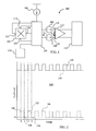
- FIG. 2 depicts a graph 140 of the V 2 142 over time for operation of the Hall effect sensor circuit 100 in the presence of a magnetic field with both V c1 and V c2 set to zero.
- the V 2 142 is a summation of a V os 144 and a V h 146.
- the V os 144 is a substantially constant DC value.
- the time varying characteristic of the V h 146 is a result of the spinning current technique effected by the clock generator 116.
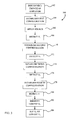
- the clock generator 116 then controls the switch matrix 104 to establish a second configuration (block 170).
- the second configuration may be, for example, the second configuration described above with respect to FIG. 2 .
- the resulting V 1 is measured and stored (block 172).
- the procedure 160 may be modified for a ⁇ various applications.
- the V c may be defined prior to placing a front end amplifier in the system.
- the procedure 160 may be performed in an area devoid of external magnetic fields. Accordingly, a single V 1 measurement may be used to identify a desired V c . Similarly, in instances wherein variation need not be initiated from a substantially zero voltage, a single V 1 measurement may also be used. The effect of such a modification is simply to establish the V c at a value somewhere within the range of voltages defined, for example, by the V 2 142 of FIG. 2 .
- the procedure 160 was performed using a Hall element 102 with four configurations, the procedure may be modified to be used with Hall elements of more or fewer connections.
Landscapes
- Physics & Mathematics (AREA)
- Condensed Matter Physics & Semiconductors (AREA)
- General Physics & Mathematics (AREA)
- Measuring Magnetic Variables (AREA)
- Hall/Mr Elements (AREA)
Claims (6)
- Hallelement-Sensorschaltkreis, der Folgendes umfasst:- ein Hallelement (202);- eine Hallelementquelle (206);- eine Schaltmatrix (204), die mit dem Hallelement (202) und der Hallelementquelle (206) wirkverbunden ist, um einen Spinning-Strom in dem Hallelement (202) zu erzeugen und ein Hallelementsignal von dem Hallelement (202) auf der Basis des Spinning-Stroms zu empfangen;- einen Frontend-Verstärker (212), der einen ersten Eingang (226), der mit einem ersten Schaltmatrixausgang wirkverbunden ist, und einen zweiten Eingang (228), der mit einem zweiten Schaltmatrixausgang wirkverbunden ist, umfassst; und- mindestens eine Spannungsquelle (218, 220), die mit dem Frontend-Verstärker (212) an einer Stelle in dem Hallelementsensorschaltkreis zwischen der Schaltmatrix (204) und dem Frontend-Verstärker (212) wirkverbunden ist; und- einen Taktsignalgenerator (216), der mit der Schaltmatrix (204) wirkgekoppelt ist und dafür ausgebildet ist, die Schaltmatrix (204) zu steuern, den Spinning-Strom bereitzustellen;
gekennzeichnet durch
einen ersten Schalter (222) mit einer ersten Position, in welcher der erste Eingang (226) des Verstärkers (212) durch den ersten Schalter (222) elektrisch mit Erde verbunden ist, und einer zweiten Position, in welcher der erste Eingang (226) des Verstärkers (212) nicht durch den ersten Schalter (222) elektrisch mit Erde verbunden ist; und
einen zweiten Schalter (224) mit einer dritten Position, in welcher der zweiten Eingang (228) des Verstärkers (212) durch die zweiten Schalter (224) elektrisch mit Erde verbunden ist, und einer vierten Position, in welcher der zweite Eingang (228) des Verstärkers (212) nicht durch die zweiten Schalter (224) elektrisch mit Erde verbunden ist, wobei
der Taktsignalgenerator (216) mit dem ersten Schalter (222) wirkverbunden ist, um den ersten Schalter (222) zwischen der ersten und der zweiten Position zu steuern, und
der Taktsignalgenerator (216) mit dem zweiten Schalter (224) wirkverbunden ist, um den zweiten Schalter (224) zwischen der dritten und der vierten Position zu steuern. - Sensorschaltkreis nach Anspruch 1, wobei die mindestens eine Spannungsquelle (218, 220) Folgendes umfasst:- einen ersten Kondensator (218), der elektrisch mit dem ersten Eingang (226) des Verstärkers (212) verbunden ist; und- einen zweiten Kondensator (220), der elektrisch mit einem zweiten Eingang (228) des Verstärkers (212) gekoppelt ist.
- Sensorschaltkreis nach Anspruch 1, wobei die Hallelementquelle (206) eine elektrische Stromquelle ist.
- Sensorschaltkreis nach Anspruch 1, wobei die Hallelementquelle (206) eine elektrische Spannungsquelle ist.
- Sensorschaltkreis nach Anspruch 1, wobei der Taktgenerator (216) dafür ausgebildet ist, die Schaltmatrix durch eine Abfolge von Ausgestaltungen so zu steuern (204), dass ein Kontakt des Hallelements (202) der Reihe nach mit der Hallelementquelle (206), dem ersten Eingang, Erde und dem zweiten Eingang wirkverbunden wird.
- Verfahren zum Erzeugen eines Signals auf der Basis eines Magnetfeldes, wobei das Verfahren Folgendes umfasst:- Herstellen eines ersten Spannungssignals auf der Basis einer Versatzspannung, die einem Hallelementsensorschaltkreis (200) zugeordnet ist;- Erzeugen eines Ausgangssignals aus dem Halleffektelement (202) in dem Hallelementsensorschaltkreis (200) auf der Basis eines Magnetfeldes unter Verwendung eines Spinning-Stroms;- Modifizieren des Ausgangssignals unter Verwendung der hergestellten ersten Spannung; und- Verstärken des modifizierten Ausgangssignals;
dadurch gekennzeichnet, dass das Herstellen eines ersten Spannungssignals Folgendes umfasst:• Verbinden eines ersten Eingangs eines Frontend-Verstärkers (212) mit Erde unter Verwendung eines ersten Schalters (222);• Verbinden eines zweiten Eingangs des Frontend-Verstärkers (212) mit Erde unter Verwendung eines zweiten Schalters (224);• Laden eines ersten Kondensators (218), der mit einer Schaltmatrix (204) und mit dem ersten Schalter (222) wirkverbunden ist, mit dem Halleffektelement (202); und• Laden eines zweiten Kondensators (220), der mit der Schaltmatrix (204) und mit dem zweiten Schalter (224) wirkverbunden ist, mit dem Halleffektelement (202).
Priority Applications (2)
| Application Number | Priority Date | Filing Date | Title |
|---|---|---|---|
| EP14183049.7A EP2837946B1 (de) | 2010-12-21 | 2011-12-10 | Halleffektsensor mit reduziertem Versatz |
| EP16160426.9A EP3064954B1 (de) | 2010-12-21 | 2011-12-10 | Halleffektsensor mit reduziertem offset |
Applications Claiming Priority (2)
| Application Number | Priority Date | Filing Date | Title |
|---|---|---|---|
| US12/974,239 US8633687B2 (en) | 2010-12-21 | 2010-12-21 | Hall Effect sensor with reduced offset |
| PCT/US2011/064294 WO2012087623A1 (en) | 2010-12-21 | 2011-12-10 | Hall effect sensor with reduced offset |
Related Child Applications (2)
| Application Number | Title | Priority Date | Filing Date |
|---|---|---|---|
| EP14183049.7A Division EP2837946B1 (de) | 2010-12-21 | 2011-12-10 | Halleffektsensor mit reduziertem Versatz |
| EP16160426.9A Division EP3064954B1 (de) | 2010-12-21 | 2011-12-10 | Halleffektsensor mit reduziertem offset |
Publications (2)
| Publication Number | Publication Date |
|---|---|
| EP2656091A1 EP2656091A1 (de) | 2013-10-30 |
| EP2656091B1 true EP2656091B1 (de) | 2014-09-03 |
Family
ID=45420995
Family Applications (3)
| Application Number | Title | Priority Date | Filing Date |
|---|---|---|---|
| EP16160426.9A Active EP3064954B1 (de) | 2010-12-21 | 2011-12-10 | Halleffektsensor mit reduziertem offset |
| EP11802618.6A Active EP2656091B1 (de) | 2010-12-21 | 2011-12-10 | Halleffektsensor mit reduziertem versatz |
| EP14183049.7A Active EP2837946B1 (de) | 2010-12-21 | 2011-12-10 | Halleffektsensor mit reduziertem Versatz |
Family Applications Before (1)
| Application Number | Title | Priority Date | Filing Date |
|---|---|---|---|
| EP16160426.9A Active EP3064954B1 (de) | 2010-12-21 | 2011-12-10 | Halleffektsensor mit reduziertem offset |
Family Applications After (1)
| Application Number | Title | Priority Date | Filing Date |
|---|---|---|---|
| EP14183049.7A Active EP2837946B1 (de) | 2010-12-21 | 2011-12-10 | Halleffektsensor mit reduziertem Versatz |
Country Status (3)
| Country | Link |
|---|---|
| US (1) | US8633687B2 (de) |
| EP (3) | EP3064954B1 (de) |
| WO (1) | WO2012087623A1 (de) |
Families Citing this family (7)
| Publication number | Priority date | Publication date | Assignee | Title |
|---|---|---|---|---|
| JP6004758B2 (ja) * | 2012-06-07 | 2016-10-12 | エスアイアイ・セミコンダクタ株式会社 | 磁気センサ |
| WO2015035169A1 (en) * | 2013-09-06 | 2015-03-12 | Robert Bosch Gmbh | Low offset and high sensitivity vertical hall effect sensor |
| US10191505B2 (en) * | 2014-11-07 | 2019-01-29 | Diodes Incorporated | Hall sensor chip with timing control |
| KR102169800B1 (ko) * | 2015-06-16 | 2020-10-26 | 주식회사 해치텍 | 홀 소자 제어 방법 및 이를 이용한 자기 검출 장치 |
| EP3358309B1 (de) | 2017-02-06 | 2019-04-24 | Melexis Technologies SA | Methode und schaltkreis zum vorspannen und auslesen einer resistiven sensorstruktur |
| IT201700071213A1 (it) * | 2017-06-26 | 2018-12-26 | St Microelectronics Srl | Circuito di lettura per sensori hall, dispositivo e procedimento corrispondenti |
| IT201800007246A1 (it) * | 2018-07-17 | 2020-01-17 | Sensore di hall, dispositivi e procedimento corrispondenti |
Family Cites Families (6)
| Publication number | Priority date | Publication date | Assignee | Title |
|---|---|---|---|---|
| EP0548391B1 (de) * | 1991-12-21 | 1997-07-23 | Deutsche ITT Industries GmbH | Offsetkompensierter Hallsensor |
| US6064202A (en) | 1997-09-09 | 2000-05-16 | Physical Electronics Laboratory | Spinning current method of reducing the offset voltage of a hall device |
| DE10032530C2 (de) | 2000-07-05 | 2002-10-24 | Infineon Technologies Ag | Verstärkerschaltung mit Offsetkompensation |
| DE10223767B4 (de) * | 2002-05-28 | 2004-10-21 | Infineon Technologies Ag | Schaltungsanordnung zum Verarbeiten eines Signals eines Sensors |
| DE102006059421B4 (de) | 2006-07-14 | 2011-06-01 | Fraunhofer-Gesellschaft zur Förderung der angewandten Forschung e.V. | Verfahren zur Verarbeitung von Offset-behafteten Sensorsignalen sowie für die Durchführung des Verfahrens ausgebildete Sensoranordnung |
| JP2008309626A (ja) | 2007-06-14 | 2008-12-25 | Oki Electric Ind Co Ltd | 感磁出力ic |
-
2010
- 2010-12-21 US US12/974,239 patent/US8633687B2/en active Active
-
2011
- 2011-12-10 WO PCT/US2011/064294 patent/WO2012087623A1/en not_active Ceased
- 2011-12-10 EP EP16160426.9A patent/EP3064954B1/de active Active
- 2011-12-10 EP EP11802618.6A patent/EP2656091B1/de active Active
- 2011-12-10 EP EP14183049.7A patent/EP2837946B1/de active Active
Also Published As
| Publication number | Publication date |
|---|---|
| EP2837946A1 (de) | 2015-02-18 |
| EP3064954B1 (de) | 2021-08-11 |
| EP2837946B1 (de) | 2016-03-16 |
| US20120153945A1 (en) | 2012-06-21 |
| US8633687B2 (en) | 2014-01-21 |
| EP2656091A1 (de) | 2013-10-30 |
| WO2012087623A1 (en) | 2012-06-28 |
| EP3064954A1 (de) | 2016-09-07 |
Similar Documents
| Publication | Publication Date | Title |
|---|---|---|
| EP2656091B1 (de) | Halleffektsensor mit reduziertem versatz | |
| EP3457088B1 (de) | Reduzierung von durch chopper-stabilisierung erzeugter welligkeit | |
| EP3679653B1 (de) | Verfahren und vorrichtung zur reduzierung des einflusses eines gleichtaktsignals auf ein differenzsignal und auf systeme mit einer solchen vorrichtung | |
| US10429483B2 (en) | Internal integrated circuit resistance calibration | |
| US20060232278A1 (en) | method and apparatus for providing stable voltage to analytical system | |
| US20090009163A1 (en) | Magnetic sensing device and electronic compass using the same | |
| CN111051820B (zh) | 电桥传感器的检测电路、芯片及检测系统 | |
| US11169218B2 (en) | Current monitor with fault detection | |
| EP3012971A1 (de) | Verstärkerschaltung und verstärkerschaltungschip | |
| US9863808B2 (en) | Output-current detection chip for diode sensors, and diode sensor device | |
| US6982559B2 (en) | Accurate and efficient sensing circuit and method for bi-directional signals | |
| AU2012214000B2 (en) | Device and method for evaluating signals of load cells with strain gauges | |
| JP4977013B2 (ja) | 電力印加回路、及び試験装置 | |
| US20070103174A1 (en) | Direct current test apparatus | |
| JP2012105197A (ja) | 光電変換回路 | |
| CN108072790B (zh) | 一种电流测量电路和电流测量方法 | |
| US11402275B2 (en) | Sensor apparatus | |
| KR101122581B1 (ko) | 차동 차이 증폭부를 이용한 정전압 분극 회로 | |
| Xie et al. | Design of a 68 dB input dynamic range potentiostat for electrochemical biosensing | |
| JP4479086B2 (ja) | 組電池の電圧検出装置 | |
| US10302678B2 (en) | Motor control circuitry | |
| CN105680810B (zh) | 放大电路、信号放大方法及传感信号处理装置 | |
| KR102710006B1 (ko) | 임피던스 측정 장치 | |
| JP2002016452A (ja) | 増幅回路 | |
| EP2634589B1 (de) | Rückholung von Batterien aus dem Ruhemodus |
Legal Events
| Date | Code | Title | Description |
|---|---|---|---|
| PUAI | Public reference made under article 153(3) epc to a published international application that has entered the european phase |
Free format text: ORIGINAL CODE: 0009012 |
|
| 17P | Request for examination filed |
Effective date: 20130722 |
|
| AK | Designated contracting states |
Kind code of ref document: A1 Designated state(s): AL AT BE BG CH CY CZ DE DK EE ES FI FR GB GR HR HU IE IS IT LI LT LU LV MC MK MT NL NO PL PT RO RS SE SI SK SM TR |
|
| DAX | Request for extension of the european patent (deleted) | ||
| GRAP | Despatch of communication of intention to grant a patent |
Free format text: ORIGINAL CODE: EPIDOSNIGR1 |
|
| INTG | Intention to grant announced |
Effective date: 20140430 |
|
| GRAS | Grant fee paid |
Free format text: ORIGINAL CODE: EPIDOSNIGR3 |
|
| GRAA | (expected) grant |
Free format text: ORIGINAL CODE: 0009210 |
|
| AK | Designated contracting states |
Kind code of ref document: B1 Designated state(s): AL AT BE BG CH CY CZ DE DK EE ES FI FR GB GR HR HU IE IS IT LI LT LU LV MC MK MT NL NO PL PT RO RS SE SI SK SM TR |
|
| REG | Reference to a national code |
Ref country code: GB Ref legal event code: FG4D |
|
| REG | Reference to a national code |
Ref country code: CH Ref legal event code: EP Ref country code: AT Ref legal event code: REF Ref document number: 685876 Country of ref document: AT Kind code of ref document: T Effective date: 20140915 |
|
| REG | Reference to a national code |
Ref country code: IE Ref legal event code: FG4D |
|
| REG | Reference to a national code |
Ref country code: DE Ref legal event code: R096 Ref document number: 602011009714 Country of ref document: DE Effective date: 20141016 |
|
| REG | Reference to a national code |
Ref country code: AT Ref legal event code: MK05 Ref document number: 685876 Country of ref document: AT Kind code of ref document: T Effective date: 20140903 |
|
| PG25 | Lapsed in a contracting state [announced via postgrant information from national office to epo] |
Ref country code: GR Free format text: LAPSE BECAUSE OF FAILURE TO SUBMIT A TRANSLATION OF THE DESCRIPTION OR TO PAY THE FEE WITHIN THE PRESCRIBED TIME-LIMIT Effective date: 20141204 Ref country code: SE Free format text: LAPSE BECAUSE OF FAILURE TO SUBMIT A TRANSLATION OF THE DESCRIPTION OR TO PAY THE FEE WITHIN THE PRESCRIBED TIME-LIMIT Effective date: 20140903 Ref country code: FI Free format text: LAPSE BECAUSE OF FAILURE TO SUBMIT A TRANSLATION OF THE DESCRIPTION OR TO PAY THE FEE WITHIN THE PRESCRIBED TIME-LIMIT Effective date: 20140903 Ref country code: LT Free format text: LAPSE BECAUSE OF FAILURE TO SUBMIT A TRANSLATION OF THE DESCRIPTION OR TO PAY THE FEE WITHIN THE PRESCRIBED TIME-LIMIT Effective date: 20140903 Ref country code: ES Free format text: LAPSE BECAUSE OF FAILURE TO SUBMIT A TRANSLATION OF THE DESCRIPTION OR TO PAY THE FEE WITHIN THE PRESCRIBED TIME-LIMIT Effective date: 20140903 Ref country code: NO Free format text: LAPSE BECAUSE OF FAILURE TO SUBMIT A TRANSLATION OF THE DESCRIPTION OR TO PAY THE FEE WITHIN THE PRESCRIBED TIME-LIMIT Effective date: 20141203 |
|
| REG | Reference to a national code |
Ref country code: NL Ref legal event code: VDEP Effective date: 20140903 |
|
| REG | Reference to a national code |
Ref country code: LT Ref legal event code: MG4D |
|
| PG25 | Lapsed in a contracting state [announced via postgrant information from national office to epo] |
Ref country code: RS Free format text: LAPSE BECAUSE OF FAILURE TO SUBMIT A TRANSLATION OF THE DESCRIPTION OR TO PAY THE FEE WITHIN THE PRESCRIBED TIME-LIMIT Effective date: 20140903 Ref country code: CY Free format text: LAPSE BECAUSE OF FAILURE TO SUBMIT A TRANSLATION OF THE DESCRIPTION OR TO PAY THE FEE WITHIN THE PRESCRIBED TIME-LIMIT Effective date: 20140903 Ref country code: HR Free format text: LAPSE BECAUSE OF FAILURE TO SUBMIT A TRANSLATION OF THE DESCRIPTION OR TO PAY THE FEE WITHIN THE PRESCRIBED TIME-LIMIT Effective date: 20140903 Ref country code: AT Free format text: LAPSE BECAUSE OF FAILURE TO SUBMIT A TRANSLATION OF THE DESCRIPTION OR TO PAY THE FEE WITHIN THE PRESCRIBED TIME-LIMIT Effective date: 20140903 Ref country code: LV Free format text: LAPSE BECAUSE OF FAILURE TO SUBMIT A TRANSLATION OF THE DESCRIPTION OR TO PAY THE FEE WITHIN THE PRESCRIBED TIME-LIMIT Effective date: 20140903 |
|
| PG25 | Lapsed in a contracting state [announced via postgrant information from national office to epo] |
Ref country code: NL Free format text: LAPSE BECAUSE OF FAILURE TO SUBMIT A TRANSLATION OF THE DESCRIPTION OR TO PAY THE FEE WITHIN THE PRESCRIBED TIME-LIMIT Effective date: 20140903 |
|
| PG25 | Lapsed in a contracting state [announced via postgrant information from national office to epo] |
Ref country code: PT Free format text: LAPSE BECAUSE OF FAILURE TO SUBMIT A TRANSLATION OF THE DESCRIPTION OR TO PAY THE FEE WITHIN THE PRESCRIBED TIME-LIMIT Effective date: 20150105 Ref country code: SK Free format text: LAPSE BECAUSE OF FAILURE TO SUBMIT A TRANSLATION OF THE DESCRIPTION OR TO PAY THE FEE WITHIN THE PRESCRIBED TIME-LIMIT Effective date: 20140903 Ref country code: EE Free format text: LAPSE BECAUSE OF FAILURE TO SUBMIT A TRANSLATION OF THE DESCRIPTION OR TO PAY THE FEE WITHIN THE PRESCRIBED TIME-LIMIT Effective date: 20140903 Ref country code: RO Free format text: LAPSE BECAUSE OF FAILURE TO SUBMIT A TRANSLATION OF THE DESCRIPTION OR TO PAY THE FEE WITHIN THE PRESCRIBED TIME-LIMIT Effective date: 20140903 Ref country code: IS Free format text: LAPSE BECAUSE OF FAILURE TO SUBMIT A TRANSLATION OF THE DESCRIPTION OR TO PAY THE FEE WITHIN THE PRESCRIBED TIME-LIMIT Effective date: 20150103 Ref country code: CZ Free format text: LAPSE BECAUSE OF FAILURE TO SUBMIT A TRANSLATION OF THE DESCRIPTION OR TO PAY THE FEE WITHIN THE PRESCRIBED TIME-LIMIT Effective date: 20140903 |
|
| PG25 | Lapsed in a contracting state [announced via postgrant information from national office to epo] |
Ref country code: PL Free format text: LAPSE BECAUSE OF FAILURE TO SUBMIT A TRANSLATION OF THE DESCRIPTION OR TO PAY THE FEE WITHIN THE PRESCRIBED TIME-LIMIT Effective date: 20140903 |
|
| REG | Reference to a national code |
Ref country code: DE Ref legal event code: R097 Ref document number: 602011009714 Country of ref document: DE |
|
| PG25 | Lapsed in a contracting state [announced via postgrant information from national office to epo] |
Ref country code: BE Free format text: LAPSE BECAUSE OF NON-PAYMENT OF DUE FEES Effective date: 20141231 |
|
| PLBE | No opposition filed within time limit |
Free format text: ORIGINAL CODE: 0009261 |
|
| STAA | Information on the status of an ep patent application or granted ep patent |
Free format text: STATUS: NO OPPOSITION FILED WITHIN TIME LIMIT |
|
| PG25 | Lapsed in a contracting state [announced via postgrant information from national office to epo] |
Ref country code: LU Free format text: LAPSE BECAUSE OF FAILURE TO SUBMIT A TRANSLATION OF THE DESCRIPTION OR TO PAY THE FEE WITHIN THE PRESCRIBED TIME-LIMIT Effective date: 20141210 Ref country code: DK Free format text: LAPSE BECAUSE OF FAILURE TO SUBMIT A TRANSLATION OF THE DESCRIPTION OR TO PAY THE FEE WITHIN THE PRESCRIBED TIME-LIMIT Effective date: 20140903 |
|
| REG | Reference to a national code |
Ref country code: CH Ref legal event code: PL |
|
| 26N | No opposition filed |
Effective date: 20150604 |
|
| PG25 | Lapsed in a contracting state [announced via postgrant information from national office to epo] |
Ref country code: IT Free format text: LAPSE BECAUSE OF FAILURE TO SUBMIT A TRANSLATION OF THE DESCRIPTION OR TO PAY THE FEE WITHIN THE PRESCRIBED TIME-LIMIT Effective date: 20140903 |
|
| REG | Reference to a national code |
Ref country code: IE Ref legal event code: MM4A |
|
| REG | Reference to a national code |
Ref country code: FR Ref legal event code: ST Effective date: 20150831 |
|
| PG25 | Lapsed in a contracting state [announced via postgrant information from national office to epo] |
Ref country code: IE Free format text: LAPSE BECAUSE OF NON-PAYMENT OF DUE FEES Effective date: 20141210 Ref country code: CH Free format text: LAPSE BECAUSE OF NON-PAYMENT OF DUE FEES Effective date: 20141231 Ref country code: LI Free format text: LAPSE BECAUSE OF NON-PAYMENT OF DUE FEES Effective date: 20141231 |
|
| PG25 | Lapsed in a contracting state [announced via postgrant information from national office to epo] |
Ref country code: FR Free format text: LAPSE BECAUSE OF NON-PAYMENT OF DUE FEES Effective date: 20141231 Ref country code: SI Free format text: LAPSE BECAUSE OF FAILURE TO SUBMIT A TRANSLATION OF THE DESCRIPTION OR TO PAY THE FEE WITHIN THE PRESCRIBED TIME-LIMIT Effective date: 20140903 |
|
| PG25 | Lapsed in a contracting state [announced via postgrant information from national office to epo] |
Ref country code: SM Free format text: LAPSE BECAUSE OF FAILURE TO SUBMIT A TRANSLATION OF THE DESCRIPTION OR TO PAY THE FEE WITHIN THE PRESCRIBED TIME-LIMIT Effective date: 20140903 |
|
| PG25 | Lapsed in a contracting state [announced via postgrant information from national office to epo] |
Ref country code: MC Free format text: LAPSE BECAUSE OF FAILURE TO SUBMIT A TRANSLATION OF THE DESCRIPTION OR TO PAY THE FEE WITHIN THE PRESCRIBED TIME-LIMIT Effective date: 20140903 |
|
| PG25 | Lapsed in a contracting state [announced via postgrant information from national office to epo] |
Ref country code: BG Free format text: LAPSE BECAUSE OF FAILURE TO SUBMIT A TRANSLATION OF THE DESCRIPTION OR TO PAY THE FEE WITHIN THE PRESCRIBED TIME-LIMIT Effective date: 20140903 |
|
| PG25 | Lapsed in a contracting state [announced via postgrant information from national office to epo] |
Ref country code: BE Free format text: LAPSE BECAUSE OF FAILURE TO SUBMIT A TRANSLATION OF THE DESCRIPTION OR TO PAY THE FEE WITHIN THE PRESCRIBED TIME-LIMIT Effective date: 20140903 Ref country code: MT Free format text: LAPSE BECAUSE OF FAILURE TO SUBMIT A TRANSLATION OF THE DESCRIPTION OR TO PAY THE FEE WITHIN THE PRESCRIBED TIME-LIMIT Effective date: 20140903 Ref country code: HU Free format text: LAPSE BECAUSE OF FAILURE TO SUBMIT A TRANSLATION OF THE DESCRIPTION OR TO PAY THE FEE WITHIN THE PRESCRIBED TIME-LIMIT; INVALID AB INITIO Effective date: 20111210 Ref country code: TR Free format text: LAPSE BECAUSE OF FAILURE TO SUBMIT A TRANSLATION OF THE DESCRIPTION OR TO PAY THE FEE WITHIN THE PRESCRIBED TIME-LIMIT Effective date: 20140903 |
|
| GBPC | Gb: european patent ceased through non-payment of renewal fee |
Effective date: 20151210 |
|
| PG25 | Lapsed in a contracting state [announced via postgrant information from national office to epo] |
Ref country code: GB Free format text: LAPSE BECAUSE OF NON-PAYMENT OF DUE FEES Effective date: 20151210 |
|
| PG25 | Lapsed in a contracting state [announced via postgrant information from national office to epo] |
Ref country code: MK Free format text: LAPSE BECAUSE OF FAILURE TO SUBMIT A TRANSLATION OF THE DESCRIPTION OR TO PAY THE FEE WITHIN THE PRESCRIBED TIME-LIMIT Effective date: 20140903 |
|
| PG25 | Lapsed in a contracting state [announced via postgrant information from national office to epo] |
Ref country code: AL Free format text: LAPSE BECAUSE OF FAILURE TO SUBMIT A TRANSLATION OF THE DESCRIPTION OR TO PAY THE FEE WITHIN THE PRESCRIBED TIME-LIMIT Effective date: 20140903 |
|
| PGFP | Annual fee paid to national office [announced via postgrant information from national office to epo] |
Ref country code: DE Payment date: 20260223 Year of fee payment: 15 |