EP2648212A1 - Semiconductor device - Google Patents
Semiconductor device Download PDFInfo
- Publication number
- EP2648212A1 EP2648212A1 EP10860383.8A EP10860383A EP2648212A1 EP 2648212 A1 EP2648212 A1 EP 2648212A1 EP 10860383 A EP10860383 A EP 10860383A EP 2648212 A1 EP2648212 A1 EP 2648212A1
- Authority
- EP
- European Patent Office
- Prior art keywords
- thickness
- region
- surface electrode
- semiconductor device
- thickness region
- Prior art date
- Legal status (The legal status is an assumption and is not a legal conclusion. Google has not performed a legal analysis and makes no representation as to the accuracy of the status listed.)
- Granted
Links
Images

Classifications
-
- H—ELECTRICITY
- H10—SEMICONDUCTOR DEVICES; ELECTRIC SOLID-STATE DEVICES NOT OTHERWISE PROVIDED FOR
- H10W—GENERIC PACKAGES, INTERCONNECTIONS, CONNECTORS OR OTHER CONSTRUCTIONAL DETAILS OF DEVICES COVERED BY CLASS H10
- H10W70/00—Package substrates; Interposers; Redistribution layers [RDL]
- H10W70/60—Insulating or insulated package substrates; Interposers; Redistribution layers
-
- H—ELECTRICITY
- H10—SEMICONDUCTOR DEVICES; ELECTRIC SOLID-STATE DEVICES NOT OTHERWISE PROVIDED FOR
- H10D—INORGANIC ELECTRIC SEMICONDUCTOR DEVICES
- H10D12/00—Bipolar devices controlled by the field effect, e.g. insulated-gate bipolar transistors [IGBT]
- H10D12/411—Insulated-gate bipolar transistors [IGBT]
- H10D12/441—Vertical IGBTs
- H10D12/461—Vertical IGBTs having non-planar surfaces, e.g. having trenches, recesses or pillars in the surfaces of the emitter, base or collector regions
- H10D12/481—Vertical IGBTs having non-planar surfaces, e.g. having trenches, recesses or pillars in the surfaces of the emitter, base or collector regions having gate structures on slanted surfaces, on vertical surfaces, or in grooves, e.g. trench gate IGBTs
-
- H—ELECTRICITY
- H10—SEMICONDUCTOR DEVICES; ELECTRIC SOLID-STATE DEVICES NOT OTHERWISE PROVIDED FOR
- H10D—INORGANIC ELECTRIC SEMICONDUCTOR DEVICES
- H10D64/00—Electrodes of devices having potential barriers
- H10D64/20—Electrodes characterised by their shapes, relative sizes or dispositions
- H10D64/23—Electrodes carrying the current to be rectified, amplified, oscillated or switched, e.g. sources, drains, anodes or cathodes
- H10D64/251—Source or drain electrodes for field-effect devices
- H10D64/252—Source or drain electrodes for field-effect devices for vertical or pseudo-vertical devices
-
- H—ELECTRICITY
- H10—SEMICONDUCTOR DEVICES; ELECTRIC SOLID-STATE DEVICES NOT OTHERWISE PROVIDED FOR
- H10W—GENERIC PACKAGES, INTERCONNECTIONS, CONNECTORS OR OTHER CONSTRUCTIONAL DETAILS OF DEVICES COVERED BY CLASS H10
- H10W72/00—Interconnections or connectors in packages
- H10W72/50—Bond wires
-
- H—ELECTRICITY
- H10—SEMICONDUCTOR DEVICES; ELECTRIC SOLID-STATE DEVICES NOT OTHERWISE PROVIDED FOR
- H10D—INORGANIC ELECTRIC SEMICONDUCTOR DEVICES
- H10D64/00—Electrodes of devices having potential barriers
- H10D64/20—Electrodes characterised by their shapes, relative sizes or dispositions
- H10D64/23—Electrodes carrying the current to be rectified, amplified, oscillated or switched, e.g. sources, drains, anodes or cathodes
-
- H—ELECTRICITY
- H10—SEMICONDUCTOR DEVICES; ELECTRIC SOLID-STATE DEVICES NOT OTHERWISE PROVIDED FOR
- H10W—GENERIC PACKAGES, INTERCONNECTIONS, CONNECTORS OR OTHER CONSTRUCTIONAL DETAILS OF DEVICES COVERED BY CLASS H10
- H10W72/00—Interconnections or connectors in packages
- H10W72/071—Connecting or disconnecting
- H10W72/075—Connecting or disconnecting of bond wires
- H10W72/07531—Techniques
- H10W72/07532—Compression bonding, e.g. thermocompression bonding
- H10W72/07533—Ultrasonic bonding, e.g. thermosonic bonding
-
- H—ELECTRICITY
- H10—SEMICONDUCTOR DEVICES; ELECTRIC SOLID-STATE DEVICES NOT OTHERWISE PROVIDED FOR
- H10W—GENERIC PACKAGES, INTERCONNECTIONS, CONNECTORS OR OTHER CONSTRUCTIONAL DETAILS OF DEVICES COVERED BY CLASS H10
- H10W72/00—Interconnections or connectors in packages
- H10W72/50—Bond wires
- H10W72/531—Shapes of wire connectors
- H10W72/533—Cross-sectional shape
- H10W72/534—Cross-sectional shape being rectangular
-
- H—ELECTRICITY
- H10—SEMICONDUCTOR DEVICES; ELECTRIC SOLID-STATE DEVICES NOT OTHERWISE PROVIDED FOR
- H10W—GENERIC PACKAGES, INTERCONNECTIONS, CONNECTORS OR OTHER CONSTRUCTIONAL DETAILS OF DEVICES COVERED BY CLASS H10
- H10W72/00—Interconnections or connectors in packages
- H10W72/50—Bond wires
- H10W72/531—Shapes of wire connectors
- H10W72/5363—Shapes of wire connectors the connected ends being wedge-shaped
-
- H—ELECTRICITY
- H10—SEMICONDUCTOR DEVICES; ELECTRIC SOLID-STATE DEVICES NOT OTHERWISE PROVIDED FOR
- H10W—GENERIC PACKAGES, INTERCONNECTIONS, CONNECTORS OR OTHER CONSTRUCTIONAL DETAILS OF DEVICES COVERED BY CLASS H10
- H10W72/00—Interconnections or connectors in packages
- H10W72/50—Bond wires
- H10W72/541—Dispositions of bond wires
- H10W72/5434—Dispositions of bond wires the connected ends being on auxiliary connecting means on bond pads, e.g. on other bond wires
-
- H—ELECTRICITY
- H10—SEMICONDUCTOR DEVICES; ELECTRIC SOLID-STATE DEVICES NOT OTHERWISE PROVIDED FOR
- H10W—GENERIC PACKAGES, INTERCONNECTIONS, CONNECTORS OR OTHER CONSTRUCTIONAL DETAILS OF DEVICES COVERED BY CLASS H10
- H10W72/00—Interconnections or connectors in packages
- H10W72/50—Bond wires
- H10W72/541—Dispositions of bond wires
- H10W72/5445—Dispositions of bond wires being orthogonal to a side surface of the chip, e.g. parallel arrangements
-
- H—ELECTRICITY
- H10—SEMICONDUCTOR DEVICES; ELECTRIC SOLID-STATE DEVICES NOT OTHERWISE PROVIDED FOR
- H10W—GENERIC PACKAGES, INTERCONNECTIONS, CONNECTORS OR OTHER CONSTRUCTIONAL DETAILS OF DEVICES COVERED BY CLASS H10
- H10W72/00—Interconnections or connectors in packages
- H10W72/50—Bond wires
- H10W72/541—Dispositions of bond wires
- H10W72/5453—Dispositions of bond wires connecting between multiple bond pads on a chip, e.g. daisy chain
-
- H—ELECTRICITY
- H10—SEMICONDUCTOR DEVICES; ELECTRIC SOLID-STATE DEVICES NOT OTHERWISE PROVIDED FOR
- H10W—GENERIC PACKAGES, INTERCONNECTIONS, CONNECTORS OR OTHER CONSTRUCTIONAL DETAILS OF DEVICES COVERED BY CLASS H10
- H10W72/00—Interconnections or connectors in packages
- H10W72/50—Bond wires
- H10W72/551—Materials of bond wires
- H10W72/552—Materials of bond wires comprising metals or metalloids, e.g. silver
-
- H—ELECTRICITY
- H10—SEMICONDUCTOR DEVICES; ELECTRIC SOLID-STATE DEVICES NOT OTHERWISE PROVIDED FOR
- H10W—GENERIC PACKAGES, INTERCONNECTIONS, CONNECTORS OR OTHER CONSTRUCTIONAL DETAILS OF DEVICES COVERED BY CLASS H10
- H10W72/00—Interconnections or connectors in packages
- H10W72/50—Bond wires
- H10W72/59—Bond pads specially adapted therefor
-
- H—ELECTRICITY
- H10—SEMICONDUCTOR DEVICES; ELECTRIC SOLID-STATE DEVICES NOT OTHERWISE PROVIDED FOR
- H10W—GENERIC PACKAGES, INTERCONNECTIONS, CONNECTORS OR OTHER CONSTRUCTIONAL DETAILS OF DEVICES COVERED BY CLASS H10
- H10W72/00—Interconnections or connectors in packages
- H10W72/90—Bond pads, in general
- H10W72/931—Shapes of bond pads
- H10W72/932—Plan-view shape, i.e. in top view
-
- H—ELECTRICITY
- H10—SEMICONDUCTOR DEVICES; ELECTRIC SOLID-STATE DEVICES NOT OTHERWISE PROVIDED FOR
- H10W—GENERIC PACKAGES, INTERCONNECTIONS, CONNECTORS OR OTHER CONSTRUCTIONAL DETAILS OF DEVICES COVERED BY CLASS H10
- H10W72/00—Interconnections or connectors in packages
- H10W72/90—Bond pads, in general
- H10W72/931—Shapes of bond pads
- H10W72/934—Cross-sectional shape, i.e. in side view
-
- H—ELECTRICITY
- H10—SEMICONDUCTOR DEVICES; ELECTRIC SOLID-STATE DEVICES NOT OTHERWISE PROVIDED FOR
- H10W—GENERIC PACKAGES, INTERCONNECTIONS, CONNECTORS OR OTHER CONSTRUCTIONAL DETAILS OF DEVICES COVERED BY CLASS H10
- H10W72/00—Interconnections or connectors in packages
- H10W72/90—Bond pads, in general
- H10W72/951—Materials of bond pads
- H10W72/952—Materials of bond pads comprising metals or metalloids, e.g. PbSn, Ag or Cu
Definitions
- the technology in the present application relates to a semiconductor device.
- a bonding wire is bonded to the upper surface of the upper surface electrode.
- the upper surface electrode and the semiconductor substrate under the bonded portion may in some cases be damaged because of stress generated when bonding wire is bonded.
- H7-201908 discloses that a cell region where a semiconductor element is formed and a dummy cell region where a semiconductor element is not formed are mixed, and a bonding wire is bonded to a surface electrode in a portion formed on the upper surface of the dummy cell region. Thereby damage of the cell region can be controlled.
- thickness of the entire upper surface electrode is increased to relax the stress generated in a bonded portion.
- a ratio of a cell region with respect to the substrate area of the semiconductor substrate decreases, and the size of the semiconductor device increases. If the thickness of the entire upper surface electrode is increased as in the case of Japanese Patent Application Publication No. 2002-222826 , the semiconductor wafer tends to warp during the steps of manufacturing the semiconductor device, because the thermal expansion coefficient of the upper surface electrode and that of the semiconductor substrate are different, therefore defects tend to occur.
- a semiconductor device disclosed in this description has a semiconductor substrate including an element region in which a semiconductor element is formed, and an upper surface electrode formed on an upper surface of the element region of the semiconductor substrate.
- the upper surface electrode has a first thickness region and a second thickness region which is thicker than the first thickness region, and a bonding wire is bonded on the second thickness region.
- the bonding wire is bonded on the second thickness region of the upper surface electrode, which is formed on the upper surface of the element region of the semiconductor substrate. Since the second thickness region is thicker than the first thickness region, stress, generated on the second thickness region due to bonding the bonding wire, is relaxed, and damage to the semiconductor device can be suppressed. Even if the bonding wire is bonded on the upper surface electrode formed on the surface of the element, damage to the semiconductor device can be suppressed.
- the upper surface electrode has the first thickness region that is thinner than the second thickness region, therefore the generation of warp of a semiconductor wafer during the steps of manufacturing the semiconductor device can be suppressed.
- a slit portion may be provided at a boundary between the first thickness region and the second thickness region, and the upper surface electrode of the slit portion may be thinner than the upper surface electrode of the first thickness region. If the slit portion is provided, generation of warp of a semiconductor during the steps of manufacturing the semiconductor device can be further suppressed by the slit portion.
- a semiconductor device disclosed in this description has: a semiconductor substrate including an element region in which a semiconductor element is formed; and an upper surface electrode formed on an upper surface of the element region of the semiconductor substrate.
- the upper surface electrode has a first thickness region and a second thickness region.
- the upper surface electrode in the second thickness region is thicker than the upper surface electrode in the first thickness region.
- a bonding wire is bonded on at least a part of the upper surface of the upper surface electrode in the second thickness region.
- the upper surface electrode is not limited to a special electrode only if a bonding wire can be bonded on the upper surface of the electrode, and may be an electrode formed on the upper surface of a main cell region of the semiconductor substrate, or may be an electrode formed on the upper surface of a sense cell region.
- each of the upper surface electrodes on which a bonding wire is bonded has a first thickness region and a second thickness region.
- a bonding region, in which the upper surface electrode and the bonding wire are bonded is included in the second thickness region.
- a bonding wire may be bonded on the upper surface of at least one second thickness region out of the plurality of second thickness regions, or bonding wires may be bonded on the upper surfaces of all the second thickness surfaces respectively.
- the shape of the bonding wire may be linear, such as a metal line, or may be a tape or ribbon.
- the semiconductor device is a semiconductor device where a bonding wire is bonded on the upper electrode, and is not restricted by the type of semiconductor element (e.g. IGBT, MOS, diode) that is formed on the semiconductor substrate.
- a semiconductor device 10 has: a semiconductor substrate 100; upper surface electrodes 121 to 123 formed on the upper surface of a semiconductor substrate 100; and a rear surface electrode 130 formed on a rear surface of the semiconductor substrate 100.
- the principal component of the upper surface electrodes 121 to 123 and the rear surface electrode 130 is metal.
- the semiconductor substrate 100 includes a plurality of main cell regions 111 to 113 in which a semiconductor element is formed, and a non-cell region 102 in which a semiconductor element is not formed.
- the upper surface electrodes 121 to 123 are formed on the upper surfaces of the main cell regions 111 to 113 respectively. A part of the upper surface electrodes 121 to 123 may extend to the upper surface of the non-cell region 102.
- a gate pad is disposed on the upper surface of the semiconductor device 10, and a small signal pad, such as a sense pad, may also be disposed, although this is not illustrated.
- a trench gate type IGBT is formed in the main cell region 113 of the semiconductor substrate 100.
- a collector layer 11, a drift layer 12 and a body layer 13 are provided sequentially from the rear surface side, and an emitter layer 14 is formed in a part of the upper surface of the body layer 13.
- the body layer 13 and the emitter layer 14 are electrically connected with the upper surface electrode 123.
- a trench gate 15 penetrates through the emitter layer 14 and the body layer 13 from the upper surface side of the semiconductor substrate 100, and reaches the drift layer 12.
- a gate electrode coated with insulation film is filled inside the trench gate 15.
- the gate electrode is insulated from the upper surface electrode 123 by an insulation film 16.
- a trench gate type IGBT is also formed in the main cell regions 111 and 112, just like the main cell region 113.
- the upper surface electrodes 121 to 123 are the main emitter electrodes of the main cell regions 111 to 113 respectnvely.
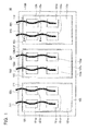
- the surface electrodes 121 to 123 have second thickness regions 121a to 121d, 122a to 122d and 123a to 123d, and first thickness regions 121e, 122e and 123e respectively.
- Bonding wires 221 to 226 are bonded on the upper surfaces of the second thickness regions 121 a to 121d, 122a to 122d and 123a to 123d respectively.
- the bonding wires 221 to 226 are metal wires.
- Each of the second thickness regions 121a to 121d, 122a to 122d and 123a to 123d is rectangular in a plan view of the semiconductor device.
- the bonding wires 221 to 226 are bonded to the center of the upper surfaces of the second thickness regions 121a to 121d, 122a to 122d and 123 a to 123d respectively.
- the bonding wire 221 is bonded on the upper surfaces of the second thickness region 121a and the second thickness region 121c located under the bonding wire 221 respectively, and is curved up in an area between the second thickness region 121a and the second thickness region 121c.
- the bonding wires 222 to 226 are bonded to the upper surfaces of the second thickness regions 121 b, 121 d, 122a to 122d and 123a to 123d, located under the bonding wires 222 to 226 respectively, and are curved up in areas between the second thickness regions on which the bonding wires are bonded respectively.
- the bonding wire is not bonded to the first thickness regions 121 e, 122e and 123e.
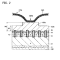
- the thickness W2 of the upper surface electrode in the second thickness region 121 is thicker than the thickness W1 of the upper surface electrode in the first thickness region 122 (W2 > W1).
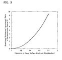
- FIG. 3 shows the result of testing the relationship between the thickness of the upper surface electrode and the breakdown resistance improvement ratio of the semiconductor device.
- the aluminum electrode is used for the upper surface electrode, and the bonding wire is bonded on the upper surface of the upper surface electrode formed on the upper surface of the element region of the semiconductor substrate using an ultrasonic bonding technique.
- the abscissa indicates the thickness of the upper surface electrode, and is the ratio with respect to the thickness of a conventional upper surface electrode.
- the ordinate indicates the element breakdown resistance improvement ratio of the semiconductor device.
- the element breakdown resistance improvement ratio is a numeric value (%) determined by dividing the ratio of the number of elements broken down in the semiconductor device of which upper surface electrode has a predetermined thickness, by the ratio of the number of elements broken down in the semiconductor device of which upper surface electrode has a conventional thickness in a case where wire bonding is implemented at a predetermined bonding pressure.
- the element breakdown resistance improvement ratio of the semiconductor device increases as the thickness of the upper surface electrode increases. For example, if the thickness of the upper surface electrode is 1.4 times, the element breakdown resistance improvement ratio increases by 2%, and if the thickness of the upper surface electrode is 1.8 times, the element breakdown resistance improvement ratio increases by 9%.
- the result shown in FIG. 3 indicates that the effect to relax the stress, which is generated in an area of the upper surface electrode on which the bonding wire is bonded, increases, and the element breakdown resistance improvement ratio of the semiconductor device increases, as the thickness of the upper surface electrode increases.
- the semiconductor wafer tends to warp during the steps of manufacturing the semiconductor device, because the thermal expansion coefficient of the upper surface electrode and that of the semiconductor substrate are different, therefore defects tend to occur.
- the thickness of a semiconductor wafer is decreasing, and in some cases, the thickness is decreased down to 100 to 200 ⁇ m. As the thickness of the semiconductor wafer decreases, the semiconductor wafer warps more easily.
- the second thickness region of the upper surface electrode is thicker than the first thickness region of the upper surface electrode, therefore the stress generated in the second thickness region is relaxed.
- the upper surface electrode has a first thickness region which is thinner than the second thickness region, so the generation of warp in the semiconductor wafer during the steps of manufacturing the semiconductor device is suppressed. In other words, both an improvement in the element breakdown resistance of the semiconductor device and a suppression of the generation of warp of the semiconductor wafer can be implemented.
- the stress generated in the second thickness region of the semiconductor device is relaxed, which allows bonding the bonding wire on the upper surface electrode formed on the upper surface of the element region, and downsizing the semiconductor device.
- W2/W1 is 1.2 or more in order to increase the strength of bonding. In terms of ease of manufacturing the upper surface electrode, it is preferable that W2/W1 is 2.0 or less.
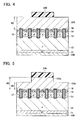
- An upper surface electrode 123 having a second thickness region 123a of which thickness is W2 and a first thickness region 123e of which thickness is W1 can easily be manufactured by the manufacturing method shown in FIG. 4 and FIG. 5 .
- an upper surface electrode film 323, of which thickness is uniformly W2 is formed on the upper surface of the semiconductor substrate 100.
- a patterned resist 330 is formed so as to cover the second thickness region 123a of the upper surface electrode film 323. If etched in this state, the upper surface electrode film 323 of the portion that is not covered by resist 330 (portion to be the first thickness region 123e) is removed. Thereby the second thickness region 123a of which thickness is W2 and the first thickness region 123e of which thickness is W1 can be formed as shown in FIG. 5 .
- a slit portion 141 may be formed in the boundary between the first thickness region 123e and the second thickness region 123a.
- the slit portion 141 may be formed in a part of the boundary between the first thickness region 123e and the second thickness region 123a, or may be formed in the entire boundary between the first thickness region 123e and the second thickness region 123a so as to surround the second thickness region 123a.
- the slit portion 141 can be formed by making the thickness of the upper surface electrode 123 in the boundary between the second thickness region 123a and the first thickness region 123e to be thinner than the thickness of the first thickness region 123e by W3.
- the thickness (W1-W3) of the upper surface electrode 123 in the slit portion 141 is 1 ⁇ m or more.
- the second thickness region is rectangular in the plan view of the semiconductor device, but the shape of the second thickness region is not limited to a rectangle, but may be a circle, an ellipse, a triangle or another polygon, or may be an irregular shape. If a gate pad and a small signal pad such as a sense pad are formed on the upper surface of the semiconductor device, the gate pad or the small signal pad is the upper surface electrode having the first thickness region and the second thickness region according to the present invention, and the bonding wire may be bonded on the second thickness region. Furthermore, in the example and the modification, a case when a bonding wire is bonded to each one of the plurality of second thickness regions was described as an example, but bonding wires need not be bonded to all of the plurality of second thickness regions respectively.
Landscapes
- Wire Bonding (AREA)
- Internal Circuitry In Semiconductor Integrated Circuit Devices (AREA)
- Electrodes Of Semiconductors (AREA)
Abstract
Description
- The technology in the present application relates to a semiconductor device.
- In order to electrically connect an upper surface electrode formed on an upper surface of a semiconductor substrate and an external terminal, a bonding wire is bonded to the upper surface of the upper surface electrode. In the bonded portion on the upper surface electrode, the upper surface electrode and the semiconductor substrate under the bonded portion may in some cases be damaged because of stress generated when bonding wire is bonded. To prevent damage of the upper surface electrode and the semiconductor substrate due to the stress generated in the bonded portion, Japanese Patent Application Publication No.
H7-201908 2002-222826 -
- Patent Document 1: Japanese Patent Application Publication No.
H7-201908 - Patent Document 2: Japanese Patent Application Publication No.
2002-222826 - If a dummy cell region is created for bonding, as in the case of Japanese Patent Application Publication No.
H7-201908 2002-222826 - A semiconductor device disclosed in this description has a semiconductor substrate including an element region in which a semiconductor element is formed, and an upper surface electrode formed on an upper surface of the element region of the semiconductor substrate. The upper surface electrode has a first thickness region and a second thickness region which is thicker than the first thickness region, and a bonding wire is bonded on the second thickness region.
- In the semiconductor device, the bonding wire is bonded on the second thickness region of the upper surface electrode, which is formed on the upper surface of the element region of the semiconductor substrate. Since the second thickness region is thicker than the first thickness region, stress, generated on the second thickness region due to bonding the bonding wire, is relaxed, and damage to the semiconductor device can be suppressed. Even if the bonding wire is bonded on the upper surface electrode formed on the surface of the element, damage to the semiconductor device can be suppressed. The upper surface electrode has the first thickness region that is thinner than the second thickness region, therefore the generation of warp of a semiconductor wafer during the steps of manufacturing the semiconductor device can be suppressed.
- A slit portion may be provided at a boundary between the first thickness region and the second thickness region, and the upper surface electrode of the slit portion may be thinner than the upper surface electrode of the first thickness region. If the slit portion is provided, generation of warp of a semiconductor during the steps of manufacturing the semiconductor device can be further suppressed by the slit portion.
-
-
FIG. 1 is a plan view of a semiconductor device according to Example 1, and shows a state of a bonding wire being bonded on an upper surface electrode; -
FIG. 2 is a cross-sectional view sectioned at the II-II line inFIG. 1 ; -
FIG. 3 shows a relationship between a thickness of the upper surface electrode and the element breakdown resistance improvement ratio of the semiconductor device; -
FIG. 4 is a diagram depicting a method for manufacturing the semiconductor device according to Example 1; -
FIG. 5 is a diagram depicting a method for manufacturing the semiconductor device according to Example 1; and -
FIG. 6 is a cross-sectional view depicting a semiconductor device according to a modification. - A semiconductor device disclosed in this description has: a semiconductor substrate including an element region in which a semiconductor element is formed; and an upper surface electrode formed on an upper surface of the element region of the semiconductor substrate. The upper surface electrode has a first thickness region and a second thickness region. The upper surface electrode in the second thickness region is thicker than the upper surface electrode in the first thickness region. A bonding wire is bonded on at least a part of the upper surface of the upper surface electrode in the second thickness region. The upper surface electrode is not limited to a special electrode only if a bonding wire can be bonded on the upper surface of the electrode, and may be an electrode formed on the upper surface of a main cell region of the semiconductor substrate, or may be an electrode formed on the upper surface of a sense cell region. If the semiconductor device has a plurality of upper surface electrodes on which a bonding wire is bonded, it is preferable that each of the upper surface electrodes on which a bonding wire is bonded has a first thickness region and a second thickness region. Required in this case is that, in a plan view of the semiconductor device, a bonding region, in which the upper surface electrode and the bonding wire are bonded, is included in the second thickness region. If the upper surface electrode has a plurality of second thickness regions, a bonding wire may be bonded on the upper surface of at least one second thickness region out of the plurality of second thickness regions, or bonding wires may be bonded on the upper surfaces of all the second thickness surfaces respectively. The shape of the bonding wire may be linear, such as a metal line, or may be a tape or ribbon. The semiconductor device is a semiconductor device where a bonding wire is bonded on the upper electrode, and is not restricted by the type of semiconductor element (e.g. IGBT, MOS, diode) that is formed on the semiconductor substrate.
- As shown in
FIG. 1 andFIG. 2 , asemiconductor device 10 has: asemiconductor substrate 100;upper surface electrodes 121 to 123 formed on the upper surface of asemiconductor substrate 100; and arear surface electrode 130 formed on a rear surface of thesemiconductor substrate 100. The principal component of theupper surface electrodes 121 to 123 and therear surface electrode 130 is metal. Thesemiconductor substrate 100 includes a plurality ofmain cell regions 111 to 113 in which a semiconductor element is formed, and anon-cell region 102 in which a semiconductor element is not formed. Theupper surface electrodes 121 to 123 are formed on the upper surfaces of themain cell regions 111 to 113 respectively. A part of theupper surface electrodes 121 to 123 may extend to the upper surface of thenon-cell region 102. A gate pad is disposed on the upper surface of thesemiconductor device 10, and a small signal pad, such as a sense pad, may also be disposed, although this is not illustrated. - As shown in
FIG. 2 , a trench gate type IGBT is formed in themain cell region 113 of thesemiconductor substrate 100. In themain cell region 113, acollector layer 11, adrift layer 12 and abody layer 13 are provided sequentially from the rear surface side, and anemitter layer 14 is formed in a part of the upper surface of thebody layer 13. Thebody layer 13 and theemitter layer 14 are electrically connected with theupper surface electrode 123. Atrench gate 15 penetrates through theemitter layer 14 and thebody layer 13 from the upper surface side of thesemiconductor substrate 100, and reaches thedrift layer 12. A gate electrode coated with insulation film is filled inside thetrench gate 15. The gate electrode is insulated from theupper surface electrode 123 by aninsulation film 16. A trench gate type IGBT is also formed in themain cell regions 111 and 112, just like themain cell region 113. Theupper surface electrodes 121 to 123 are the main emitter electrodes of themain cell regions 111 to 113 respectnvely. - The
surface electrodes 121 to 123 havesecond thickness regions 121a to 121d, 122a to 122d and 123a to 123d, andfirst thickness regions Bonding wires 221 to 226 are bonded on the upper surfaces of thesecond thickness regions 121 a to 121d, 122a to 122d and 123a to 123d respectively. Thebonding wires 221 to 226 are metal wires. Each of thesecond thickness regions 121a to 121d, 122a to 122d and 123a to 123d is rectangular in a plan view of the semiconductor device. Thebonding wires 221 to 226 are bonded to the center of the upper surfaces of thesecond thickness regions 121a to 121d, 122a to 122d and 123 a to 123d respectively. Thebonding wire 221 is bonded on the upper surfaces of thesecond thickness region 121a and thesecond thickness region 121c located under thebonding wire 221 respectively, and is curved up in an area between thesecond thickness region 121a and thesecond thickness region 121c. In the same manner, thebonding wires 222 to 226 are bonded to the upper surfaces of thesecond thickness regions bonding wires 222 to 226 respectively, and are curved up in areas between the second thickness regions on which the bonding wires are bonded respectively. The bonding wire is not bonded to thefirst thickness regions second thickness region 121 is thicker than the thickness W1 of the upper surface electrode in the first thickness region 122 (W2 > W1). -
FIG. 3 shows the result of testing the relationship between the thickness of the upper surface electrode and the breakdown resistance improvement ratio of the semiconductor device. The aluminum electrode is used for the upper surface electrode, and the bonding wire is bonded on the upper surface of the upper surface electrode formed on the upper surface of the element region of the semiconductor substrate using an ultrasonic bonding technique. The abscissa indicates the thickness of the upper surface electrode, and is the ratio with respect to the thickness of a conventional upper surface electrode. The ordinate indicates the element breakdown resistance improvement ratio of the semiconductor device. The element breakdown resistance improvement ratio is a numeric value (%) determined by dividing the ratio of the number of elements broken down in the semiconductor device of which upper surface electrode has a predetermined thickness, by the ratio of the number of elements broken down in the semiconductor device of which upper surface electrode has a conventional thickness in a case where wire bonding is implemented at a predetermined bonding pressure. AsFIG. 3 shows, the element breakdown resistance improvement ratio of the semiconductor device increases as the thickness of the upper surface electrode increases. For example, if the thickness of the upper surface electrode is 1.4 times, the element breakdown resistance improvement ratio increases by 2%, and if the thickness of the upper surface electrode is 1.8 times, the element breakdown resistance improvement ratio increases by 9%. The result shown inFIG. 3 indicates that the effect to relax the stress, which is generated in an area of the upper surface electrode on which the bonding wire is bonded, increases, and the element breakdown resistance improvement ratio of the semiconductor device increases, as the thickness of the upper surface electrode increases. - On the other hand, if the thickness of the entire upper surface electrode increases, the semiconductor wafer tends to warp during the steps of manufacturing the semiconductor device, because the thermal expansion coefficient of the upper surface electrode and that of the semiconductor substrate are different, therefore defects tend to occur. Recently there is a striking tendency that the thickness of a semiconductor wafer is decreasing, and in some cases, the thickness is decreased down to 100 to 200 µm. As the thickness of the semiconductor wafer decreases, the semiconductor wafer warps more easily.
- In this example, the second thickness region of the upper surface electrode is thicker than the first thickness region of the upper surface electrode, therefore the stress generated in the second thickness region is relaxed. The upper surface electrode has a first thickness region which is thinner than the second thickness region, so the generation of warp in the semiconductor wafer during the steps of manufacturing the semiconductor device is suppressed. In other words, both an improvement in the element breakdown resistance of the semiconductor device and a suppression of the generation of warp of the semiconductor wafer can be implemented. The stress generated in the second thickness region of the semiconductor device is relaxed, which allows bonding the bonding wire on the upper surface electrode formed on the upper surface of the element region, and downsizing the semiconductor device.
- In the case of bonding the bonding wire by ultrasonic bonding, it is preferable that W2/W1 is 1.2 or more in order to increase the strength of bonding. In terms of ease of manufacturing the upper surface electrode, it is preferable that W2/W1 is 2.0 or less.
- An
upper surface electrode 123 having asecond thickness region 123a of which thickness is W2 and afirst thickness region 123e of which thickness is W1 can easily be manufactured by the manufacturing method shown inFIG. 4 and FIG. 5 . First asFIG. 4 shows, an uppersurface electrode film 323, of which thickness is uniformly W2, is formed on the upper surface of thesemiconductor substrate 100. Then a patterned resist 330 is formed so as to cover thesecond thickness region 123a of the uppersurface electrode film 323. If etched in this state, the uppersurface electrode film 323 of the portion that is not covered by resist 330 (portion to be thefirst thickness region 123e) is removed. Thereby thesecond thickness region 123a of which thickness is W2 and thefirst thickness region 123e of which thickness is W1 can be formed as shown inFIG. 5 . - As shown in
FIG. 6 , aslit portion 141 may be formed in the boundary between thefirst thickness region 123e and thesecond thickness region 123a. Theslit portion 141 may be formed in a part of the boundary between thefirst thickness region 123e and thesecond thickness region 123a, or may be formed in the entire boundary between thefirst thickness region 123e and thesecond thickness region 123a so as to surround thesecond thickness region 123a. By forming the slit portion, the effect to relax warp of the wafer during the steps of manufacturing the semiconductor device improves. For example, as shown inFIG. 6 , theslit portion 141 can be formed by making the thickness of theupper surface electrode 123 in the boundary between thesecond thickness region 123a and thefirst thickness region 123e to be thinner than the thickness of thefirst thickness region 123e by W3. In this case, it is preferable that the thickness (W1-W3) of theupper surface electrode 123 in theslit portion 141 is 1 µm or more. - In the example and in the modification described above, the second thickness region is rectangular in the plan view of the semiconductor device, but the shape of the second thickness region is not limited to a rectangle, but may be a circle, an ellipse, a triangle or another polygon, or may be an irregular shape. If a gate pad and a small signal pad such as a sense pad are formed on the upper surface of the semiconductor device, the gate pad or the small signal pad is the upper surface electrode having the first thickness region and the second thickness region according to the present invention, and the bonding wire may be bonded on the second thickness region. Furthermore, in the example and the modification, a case when a bonding wire is bonded to each one of the plurality of second thickness regions was described as an example, but bonding wires need not be bonded to all of the plurality of second thickness regions respectively.
- While embodiments of the present invention have been described in detail, such embodiments are merely illustrative and are not intended to limit the scope of claims. Techniques described in the scope of claims include various modifications and changes made to the specific examples illustrated above.
- It is to be understood that the technical elements described in the present description and the drawings exhibit technical usefulness solely or in various combinations thereof and shall not be limited to the combinations described in the claims at the time of filing. Furthermore, the techniques illustrated in the present description and the drawings are to achieve a plurality of objectives at the same time, whereby technical usefulness is exhibited by attaining any one of such objectives.
Claims (3)
- A semiconductor device comprising:a semiconductor substrate including an element region in which a semiconductor element is formed, andan upper surface electrode formed on an upper surface of the element region of the semiconductor substrate, whereinthe upper surface electrode comprises a first thickness region and a second thickness region which is thicker than the first thickness region, anda bonding wire is bonded on the second thickness region.
- The semiconductor device according to claim 1, wherein
a slit portion is provided at a boundary between the first thickness region and the second thickness region in the upper surface electrode. - The semiconductor device according to claim 1 or 2, wherein
the bonding wire is bonded to the upper surface electrode by an ultrasonic bonding.
Applications Claiming Priority (1)
| Application Number | Priority Date | Filing Date | Title |
|---|---|---|---|
| PCT/JP2010/071240 WO2012073302A1 (en) | 2010-11-29 | 2010-11-29 | Semiconductor device |
Publications (3)
| Publication Number | Publication Date |
|---|---|
| EP2648212A1 true EP2648212A1 (en) | 2013-10-09 |
| EP2648212A4 EP2648212A4 (en) | 2014-05-07 |
| EP2648212B1 EP2648212B1 (en) | 2019-07-03 |
Family
ID=46171290
Family Applications (1)
| Application Number | Title | Priority Date | Filing Date |
|---|---|---|---|
| EP10860383.8A Not-in-force EP2648212B1 (en) | 2010-11-29 | 2010-11-29 | A bonding wire bonded to an upper surface electrode with a slit |
Country Status (5)
| Country | Link |
|---|---|
| US (1) | US8836150B2 (en) |
| EP (1) | EP2648212B1 (en) |
| JP (1) | JPWO2012073302A1 (en) |
| CN (1) | CN103229286B (en) |
| WO (1) | WO2012073302A1 (en) |
Families Citing this family (3)
| Publication number | Priority date | Publication date | Assignee | Title |
|---|---|---|---|---|
| JP6246617B2 (en) * | 2014-02-27 | 2017-12-13 | 株式会社豊田中央研究所 | Semiconductor chip with surface electrode |
| JP6665457B2 (en) * | 2015-09-16 | 2020-03-13 | 富士電機株式会社 | Semiconductor device |
| JP7280261B2 (en) * | 2018-07-12 | 2023-05-23 | ローム株式会社 | Semiconductor elements and semiconductor devices |
Family Cites Families (16)
| Publication number | Priority date | Publication date | Assignee | Title |
|---|---|---|---|---|
| JPS6119136A (en) | 1984-07-05 | 1986-01-28 | Toshiba Corp | Wire-bonding method for semiconductor device and bonding pad to be used for that |
| JPS63141330A (en) * | 1986-12-03 | 1988-06-13 | Nec Corp | Semiconductor integrated circuit device |
| JPS63244853A (en) * | 1987-03-31 | 1988-10-12 | Nec Corp | Semiconductor integrated circuit device |
| JPH06216188A (en) | 1993-01-19 | 1994-08-05 | Nec Kansai Ltd | Semiconductor device and manufacture thereof |
| JPH06350379A (en) * | 1993-06-03 | 1994-12-22 | Tdk Corp | Surface acoustic wave element lead wire mounting structure |
| DE69321966T2 (en) | 1993-12-24 | 1999-06-02 | Consorzio Per La Ricerca Sulla Microelettronica Nel Mezzogiorno, Catania | Power semiconductor device |
| JP2000323519A (en) | 1999-05-07 | 2000-11-24 | Nec Ic Microcomput Syst Ltd | Semiconductor integrated circuit device |
| JP4221904B2 (en) | 2001-01-29 | 2009-02-12 | 富士電機デバイステクノロジー株式会社 | Semiconductor device and manufacturing method thereof |
| JP3719994B2 (en) * | 2001-12-28 | 2005-11-24 | 株式会社東芝 | Semiconductor device |
| JP4060093B2 (en) | 2002-02-28 | 2008-03-12 | Tdk株式会社 | Static eliminator |
| JP2004111885A (en) | 2002-07-23 | 2004-04-08 | Toshiba Corp | Semiconductor device |
| WO2006046302A1 (en) * | 2004-10-29 | 2006-05-04 | Spansion Llc | Semiconductor device and manufacturing method therefor |
| JP4533804B2 (en) * | 2005-06-02 | 2010-09-01 | セイコーエプソン株式会社 | Semiconductor device and manufacturing method thereof |
| JP2007035909A (en) | 2005-07-27 | 2007-02-08 | Seiko Epson Corp | Electronic device and method for manufacturing electronic device |
| JP4455488B2 (en) * | 2005-12-19 | 2010-04-21 | 三菱電機株式会社 | Semiconductor device |
| JP2010062362A (en) | 2008-09-04 | 2010-03-18 | Toyota Motor Corp | Semiconductor device and method of manufacturing the same |
-
2010
- 2010-11-29 EP EP10860383.8A patent/EP2648212B1/en not_active Not-in-force
- 2010-11-29 CN CN201080070413.7A patent/CN103229286B/en not_active Expired - Fee Related
- 2010-11-29 JP JP2012546585A patent/JPWO2012073302A1/en active Pending
- 2010-11-29 WO PCT/JP2010/071240 patent/WO2012073302A1/en not_active Ceased
- 2010-11-29 US US13/989,962 patent/US8836150B2/en active Active
Also Published As
| Publication number | Publication date |
|---|---|
| EP2648212A4 (en) | 2014-05-07 |
| CN103229286A (en) | 2013-07-31 |
| CN103229286B (en) | 2015-12-16 |
| US8836150B2 (en) | 2014-09-16 |
| EP2648212B1 (en) | 2019-07-03 |
| US20130241084A1 (en) | 2013-09-19 |
| WO2012073302A1 (en) | 2012-06-07 |
| JPWO2012073302A1 (en) | 2014-05-19 |
Similar Documents
| Publication | Publication Date | Title |
|---|---|---|
| EP2387255A2 (en) | Acoustic sensor and microphone | |
| CN102544002A (en) | Semiconductor device and method of manufacturing the same | |
| US20110298048A1 (en) | Semiconductor device | |
| JP5720647B2 (en) | Semiconductor device and manufacturing method thereof | |
| JP2018093135A (en) | Semiconductor device and manufacturing method of the same | |
| EP2648212B1 (en) | A bonding wire bonded to an upper surface electrode with a slit | |
| EP1968114A1 (en) | Semiconductor device | |
| CN108321187B (en) | Terminal structure with groove | |
| US9601573B2 (en) | Semiconductor device for reducing propagation time of gate input signals | |
| JP2013016580A (en) | Semiconductor device and manufacturing method of the same | |
| CN102629568B (en) | Semiconductor device | |
| EP2933840A1 (en) | Semiconductor device | |
| US20100052190A1 (en) | Semiconductor device | |
| US20180286775A1 (en) | Semiconductor module | |
| KR20170143269A (en) | Ceramic board and manufacturing method thereof | |
| US11239329B2 (en) | Semiconductor device | |
| CN112768504B (en) | Terminal structure of power semiconductor device and power semiconductor device | |
| CN110168707A (en) | Semiconductor device | |
| US20100207234A1 (en) | Semiconductor device and wire bonding method | |
| JP5683777B2 (en) | Switching assembly for high voltage aircraft ignition system and switching assembly | |
| CN109801910B (en) | Asymmetric transient voltage suppressor device and method of forming the same | |
| CN115223933B (en) | Semiconductor device and method for manufacturing the same | |
| US20240297118A1 (en) | Semiconductor element and semiconductor device | |
| EP0047886A2 (en) | Semiconductor device | |
| EP4152378A1 (en) | Semiconductor device |
Legal Events
| Date | Code | Title | Description |
|---|---|---|---|
| PUAI | Public reference made under article 153(3) epc to a published international application that has entered the european phase |
Free format text: ORIGINAL CODE: 0009012 |
|
| 17P | Request for examination filed |
Effective date: 20130606 |
|
| AK | Designated contracting states |
Kind code of ref document: A1 Designated state(s): AL AT BE BG CH CY CZ DE DK EE ES FI FR GB GR HR HU IE IS IT LI LT LU LV MC MK MT NL NO PL PT RO RS SE SI SK SM TR |
|
| DAX | Request for extension of the european patent (deleted) | ||
| A4 | Supplementary search report drawn up and despatched |
Effective date: 20140407 |
|
| RIC1 | Information provided on ipc code assigned before grant |
Ipc: H01L 23/485 20060101AFI20140401BHEP Ipc: H01L 21/3205 20060101ALN20140401BHEP Ipc: H01L 23/52 20060101ALN20140401BHEP Ipc: H01L 29/78 20060101ALN20140401BHEP Ipc: H01L 29/739 20060101ALN20140401BHEP Ipc: H01L 21/60 20060101ALN20140401BHEP |
|
| STAA | Information on the status of an ep patent application or granted ep patent |
Free format text: STATUS: EXAMINATION IS IN PROGRESS |
|
| 17Q | First examination report despatched |
Effective date: 20180226 |
|
| REG | Reference to a national code |
Ref country code: DE Ref legal event code: R079 Ref document number: 602010059899 Country of ref document: DE Free format text: PREVIOUS MAIN CLASS: H01L0021600000 Ipc: H01L0023485000 |
|
| GRAP | Despatch of communication of intention to grant a patent |
Free format text: ORIGINAL CODE: EPIDOSNIGR1 |
|
| STAA | Information on the status of an ep patent application or granted ep patent |
Free format text: STATUS: GRANT OF PATENT IS INTENDED |
|
| RIC1 | Information provided on ipc code assigned before grant |
Ipc: H01L 29/417 20060101ALI20190115BHEP Ipc: H01L 23/485 20060101AFI20190115BHEP Ipc: H01L 29/739 20060101ALI20190115BHEP Ipc: H01L 23/49 20060101ALI20190115BHEP |
|
| INTG | Intention to grant announced |
Effective date: 20190131 |
|
| RIN1 | Information on inventor provided before grant (corrected) |
Inventor name: TANAKA, HIROAKI |
|
| GRAS | Grant fee paid |
Free format text: ORIGINAL CODE: EPIDOSNIGR3 |
|
| GRAA | (expected) grant |
Free format text: ORIGINAL CODE: 0009210 |
|
| STAA | Information on the status of an ep patent application or granted ep patent |
Free format text: STATUS: THE PATENT HAS BEEN GRANTED |
|
| AK | Designated contracting states |
Kind code of ref document: B1 Designated state(s): AL AT BE BG CH CY CZ DE DK EE ES FI FR GB GR HR HU IE IS IT LI LT LU LV MC MK MT NL NO PL PT RO RS SE SI SK SM TR |
|
| REG | Reference to a national code |
Ref country code: GB Ref legal event code: FG4D |
|
| REG | Reference to a national code |
Ref country code: CH Ref legal event code: EP Ref country code: AT Ref legal event code: REF Ref document number: 1152006 Country of ref document: AT Kind code of ref document: T Effective date: 20190715 |
|
| REG | Reference to a national code |
Ref country code: IE Ref legal event code: FG4D |
|
| REG | Reference to a national code |
Ref country code: DE Ref legal event code: R096 Ref document number: 602010059899 Country of ref document: DE |
|
| REG | Reference to a national code |
Ref country code: DE Ref legal event code: R084 Ref document number: 602010059899 Country of ref document: DE |
|
| REG | Reference to a national code |
Ref country code: NL Ref legal event code: MP Effective date: 20190703 |
|
| REG | Reference to a national code |
Ref country code: LT Ref legal event code: MG4D |
|
| REG | Reference to a national code |
Ref country code: AT Ref legal event code: MK05 Ref document number: 1152006 Country of ref document: AT Kind code of ref document: T Effective date: 20190703 |
|
| PG25 | Lapsed in a contracting state [announced via postgrant information from national office to epo] |
Ref country code: PT Free format text: LAPSE BECAUSE OF FAILURE TO SUBMIT A TRANSLATION OF THE DESCRIPTION OR TO PAY THE FEE WITHIN THE PRESCRIBED TIME-LIMIT Effective date: 20191104 Ref country code: HR Free format text: LAPSE BECAUSE OF FAILURE TO SUBMIT A TRANSLATION OF THE DESCRIPTION OR TO PAY THE FEE WITHIN THE PRESCRIBED TIME-LIMIT Effective date: 20190703 Ref country code: LT Free format text: LAPSE BECAUSE OF FAILURE TO SUBMIT A TRANSLATION OF THE DESCRIPTION OR TO PAY THE FEE WITHIN THE PRESCRIBED TIME-LIMIT Effective date: 20190703 Ref country code: AT Free format text: LAPSE BECAUSE OF FAILURE TO SUBMIT A TRANSLATION OF THE DESCRIPTION OR TO PAY THE FEE WITHIN THE PRESCRIBED TIME-LIMIT Effective date: 20190703 Ref country code: NO Free format text: LAPSE BECAUSE OF FAILURE TO SUBMIT A TRANSLATION OF THE DESCRIPTION OR TO PAY THE FEE WITHIN THE PRESCRIBED TIME-LIMIT Effective date: 20191003 Ref country code: BG Free format text: LAPSE BECAUSE OF FAILURE TO SUBMIT A TRANSLATION OF THE DESCRIPTION OR TO PAY THE FEE WITHIN THE PRESCRIBED TIME-LIMIT Effective date: 20191003 Ref country code: NL Free format text: LAPSE BECAUSE OF FAILURE TO SUBMIT A TRANSLATION OF THE DESCRIPTION OR TO PAY THE FEE WITHIN THE PRESCRIBED TIME-LIMIT Effective date: 20190703 Ref country code: CZ Free format text: LAPSE BECAUSE OF FAILURE TO SUBMIT A TRANSLATION OF THE DESCRIPTION OR TO PAY THE FEE WITHIN THE PRESCRIBED TIME-LIMIT Effective date: 20190703 Ref country code: FI Free format text: LAPSE BECAUSE OF FAILURE TO SUBMIT A TRANSLATION OF THE DESCRIPTION OR TO PAY THE FEE WITHIN THE PRESCRIBED TIME-LIMIT Effective date: 20190703 Ref country code: SE Free format text: LAPSE BECAUSE OF FAILURE TO SUBMIT A TRANSLATION OF THE DESCRIPTION OR TO PAY THE FEE WITHIN THE PRESCRIBED TIME-LIMIT Effective date: 20190703 |
|
| PG25 | Lapsed in a contracting state [announced via postgrant information from national office to epo] |
Ref country code: RS Free format text: LAPSE BECAUSE OF FAILURE TO SUBMIT A TRANSLATION OF THE DESCRIPTION OR TO PAY THE FEE WITHIN THE PRESCRIBED TIME-LIMIT Effective date: 20190703 Ref country code: IS Free format text: LAPSE BECAUSE OF FAILURE TO SUBMIT A TRANSLATION OF THE DESCRIPTION OR TO PAY THE FEE WITHIN THE PRESCRIBED TIME-LIMIT Effective date: 20191103 Ref country code: LV Free format text: LAPSE BECAUSE OF FAILURE TO SUBMIT A TRANSLATION OF THE DESCRIPTION OR TO PAY THE FEE WITHIN THE PRESCRIBED TIME-LIMIT Effective date: 20190703 Ref country code: GR Free format text: LAPSE BECAUSE OF FAILURE TO SUBMIT A TRANSLATION OF THE DESCRIPTION OR TO PAY THE FEE WITHIN THE PRESCRIBED TIME-LIMIT Effective date: 20191004 Ref country code: ES Free format text: LAPSE BECAUSE OF FAILURE TO SUBMIT A TRANSLATION OF THE DESCRIPTION OR TO PAY THE FEE WITHIN THE PRESCRIBED TIME-LIMIT Effective date: 20190703 Ref country code: AL Free format text: LAPSE BECAUSE OF FAILURE TO SUBMIT A TRANSLATION OF THE DESCRIPTION OR TO PAY THE FEE WITHIN THE PRESCRIBED TIME-LIMIT Effective date: 20190703 |
|
| PG25 | Lapsed in a contracting state [announced via postgrant information from national office to epo] |
Ref country code: TR Free format text: LAPSE BECAUSE OF FAILURE TO SUBMIT A TRANSLATION OF THE DESCRIPTION OR TO PAY THE FEE WITHIN THE PRESCRIBED TIME-LIMIT Effective date: 20190703 |
|
| PG25 | Lapsed in a contracting state [announced via postgrant information from national office to epo] |
Ref country code: EE Free format text: LAPSE BECAUSE OF FAILURE TO SUBMIT A TRANSLATION OF THE DESCRIPTION OR TO PAY THE FEE WITHIN THE PRESCRIBED TIME-LIMIT Effective date: 20190703 Ref country code: DK Free format text: LAPSE BECAUSE OF FAILURE TO SUBMIT A TRANSLATION OF THE DESCRIPTION OR TO PAY THE FEE WITHIN THE PRESCRIBED TIME-LIMIT Effective date: 20190703 Ref country code: RO Free format text: LAPSE BECAUSE OF FAILURE TO SUBMIT A TRANSLATION OF THE DESCRIPTION OR TO PAY THE FEE WITHIN THE PRESCRIBED TIME-LIMIT Effective date: 20190703 Ref country code: IT Free format text: LAPSE BECAUSE OF FAILURE TO SUBMIT A TRANSLATION OF THE DESCRIPTION OR TO PAY THE FEE WITHIN THE PRESCRIBED TIME-LIMIT Effective date: 20190703 Ref country code: PL Free format text: LAPSE BECAUSE OF FAILURE TO SUBMIT A TRANSLATION OF THE DESCRIPTION OR TO PAY THE FEE WITHIN THE PRESCRIBED TIME-LIMIT Effective date: 20190703 |
|
| PG25 | Lapsed in a contracting state [announced via postgrant information from national office to epo] |
Ref country code: SK Free format text: LAPSE BECAUSE OF FAILURE TO SUBMIT A TRANSLATION OF THE DESCRIPTION OR TO PAY THE FEE WITHIN THE PRESCRIBED TIME-LIMIT Effective date: 20190703 Ref country code: IS Free format text: LAPSE BECAUSE OF FAILURE TO SUBMIT A TRANSLATION OF THE DESCRIPTION OR TO PAY THE FEE WITHIN THE PRESCRIBED TIME-LIMIT Effective date: 20200224 Ref country code: SM Free format text: LAPSE BECAUSE OF FAILURE TO SUBMIT A TRANSLATION OF THE DESCRIPTION OR TO PAY THE FEE WITHIN THE PRESCRIBED TIME-LIMIT Effective date: 20190703 |
|
| REG | Reference to a national code |
Ref country code: DE Ref legal event code: R097 Ref document number: 602010059899 Country of ref document: DE |
|
| REG | Reference to a national code |
Ref country code: CH Ref legal event code: PL |
|
| PLBE | No opposition filed within time limit |
Free format text: ORIGINAL CODE: 0009261 |
|
| STAA | Information on the status of an ep patent application or granted ep patent |
Free format text: STATUS: NO OPPOSITION FILED WITHIN TIME LIMIT |
|
| PG2D | Information on lapse in contracting state deleted |
Ref country code: IS |
|
| PG25 | Lapsed in a contracting state [announced via postgrant information from national office to epo] |
Ref country code: CH Free format text: LAPSE BECAUSE OF NON-PAYMENT OF DUE FEES Effective date: 20191130 Ref country code: LI Free format text: LAPSE BECAUSE OF NON-PAYMENT OF DUE FEES Effective date: 20191130 Ref country code: MC Free format text: LAPSE BECAUSE OF FAILURE TO SUBMIT A TRANSLATION OF THE DESCRIPTION OR TO PAY THE FEE WITHIN THE PRESCRIBED TIME-LIMIT Effective date: 20190703 Ref country code: LU Free format text: LAPSE BECAUSE OF NON-PAYMENT OF DUE FEES Effective date: 20191129 |
|
| 26N | No opposition filed |
Effective date: 20200603 |
|
| REG | Reference to a national code |
Ref country code: BE Ref legal event code: MM Effective date: 20191130 |
|
| PG25 | Lapsed in a contracting state [announced via postgrant information from national office to epo] |
Ref country code: SI Free format text: LAPSE BECAUSE OF FAILURE TO SUBMIT A TRANSLATION OF THE DESCRIPTION OR TO PAY THE FEE WITHIN THE PRESCRIBED TIME-LIMIT Effective date: 20190703 |
|
| GBPC | Gb: european patent ceased through non-payment of renewal fee |
Effective date: 20191129 |
|
| PG25 | Lapsed in a contracting state [announced via postgrant information from national office to epo] |
Ref country code: IE Free format text: LAPSE BECAUSE OF NON-PAYMENT OF DUE FEES Effective date: 20191129 Ref country code: FR Free format text: LAPSE BECAUSE OF NON-PAYMENT OF DUE FEES Effective date: 20191130 Ref country code: GB Free format text: LAPSE BECAUSE OF NON-PAYMENT OF DUE FEES Effective date: 20191129 |
|
| PG25 | Lapsed in a contracting state [announced via postgrant information from national office to epo] |
Ref country code: BE Free format text: LAPSE BECAUSE OF NON-PAYMENT OF DUE FEES Effective date: 20191130 |
|
| PG25 | Lapsed in a contracting state [announced via postgrant information from national office to epo] |
Ref country code: CY Free format text: LAPSE BECAUSE OF FAILURE TO SUBMIT A TRANSLATION OF THE DESCRIPTION OR TO PAY THE FEE WITHIN THE PRESCRIBED TIME-LIMIT Effective date: 20190703 |
|
| PG25 | Lapsed in a contracting state [announced via postgrant information from national office to epo] |
Ref country code: HU Free format text: LAPSE BECAUSE OF FAILURE TO SUBMIT A TRANSLATION OF THE DESCRIPTION OR TO PAY THE FEE WITHIN THE PRESCRIBED TIME-LIMIT; INVALID AB INITIO Effective date: 20101129 Ref country code: MT Free format text: LAPSE BECAUSE OF FAILURE TO SUBMIT A TRANSLATION OF THE DESCRIPTION OR TO PAY THE FEE WITHIN THE PRESCRIBED TIME-LIMIT Effective date: 20190703 |
|
| PGFP | Annual fee paid to national office [announced via postgrant information from national office to epo] |
Ref country code: DE Payment date: 20211005 Year of fee payment: 12 |
|
| PG25 | Lapsed in a contracting state [announced via postgrant information from national office to epo] |
Ref country code: MK Free format text: LAPSE BECAUSE OF FAILURE TO SUBMIT A TRANSLATION OF THE DESCRIPTION OR TO PAY THE FEE WITHIN THE PRESCRIBED TIME-LIMIT Effective date: 20190703 |
|
| REG | Reference to a national code |
Ref country code: DE Ref legal event code: R119 Ref document number: 602010059899 Country of ref document: DE |
|
| PG25 | Lapsed in a contracting state [announced via postgrant information from national office to epo] |
Ref country code: DE Free format text: LAPSE BECAUSE OF NON-PAYMENT OF DUE FEES Effective date: 20230601 |