EP2647741A2 - Apparatus for manufacturing silicon substrate - Google Patents
Apparatus for manufacturing silicon substrate Download PDFInfo
- Publication number
- EP2647741A2 EP2647741A2 EP12166022.9A EP12166022A EP2647741A2 EP 2647741 A2 EP2647741 A2 EP 2647741A2 EP 12166022 A EP12166022 A EP 12166022A EP 2647741 A2 EP2647741 A2 EP 2647741A2
- Authority
- EP
- European Patent Office
- Prior art keywords
- silicon substrate
- crucible
- raw material
- silicon
- molding
- Prior art date
- Legal status (The legal status is an assumption and is not a legal conclusion. Google has not performed a legal analysis and makes no representation as to the accuracy of the status listed.)
- Withdrawn
Links
- XUIMIQQOPSSXEZ-UHFFFAOYSA-N Silicon Chemical compound [Si] XUIMIQQOPSSXEZ-UHFFFAOYSA-N 0.000 title claims abstract description 246
- 229910052710 silicon Inorganic materials 0.000 title claims abstract description 246
- 239000010703 silicon Substances 0.000 title claims abstract description 246
- 239000000758 substrate Substances 0.000 title claims abstract description 166
- 238000004519 manufacturing process Methods 0.000 title claims abstract description 95
- 238000000465 moulding Methods 0.000 claims abstract description 118
- 239000002178 crystalline material Substances 0.000 claims abstract description 12
- 239000002994 raw material Substances 0.000 claims description 74
- 230000008878 coupling Effects 0.000 claims description 41
- 238000010168 coupling process Methods 0.000 claims description 41
- 238000005859 coupling reaction Methods 0.000 claims description 41
- 239000007789 gas Substances 0.000 claims description 41
- 239000011261 inert gas Substances 0.000 claims description 30
- 230000001154 acute effect Effects 0.000 claims description 10
- 229910021419 crystalline silicon Inorganic materials 0.000 claims description 9
- 238000010438 heat treatment Methods 0.000 description 26
- 238000000034 method Methods 0.000 description 26
- 238000010586 diagram Methods 0.000 description 23
- 238000001816 cooling Methods 0.000 description 16
- OKTJSMMVPCPJKN-UHFFFAOYSA-N Carbon Chemical compound [C] OKTJSMMVPCPJKN-UHFFFAOYSA-N 0.000 description 13
- 229910002804 graphite Inorganic materials 0.000 description 12
- 239000010439 graphite Substances 0.000 description 12
- 238000007711 solidification Methods 0.000 description 11
- 230000008023 solidification Effects 0.000 description 11
- 239000000463 material Substances 0.000 description 8
- 239000007788 liquid Substances 0.000 description 7
- 238000006243 chemical reaction Methods 0.000 description 5
- 229910021420 polycrystalline silicon Inorganic materials 0.000 description 5
- XKRFYHLGVUSROY-UHFFFAOYSA-N Argon Chemical compound [Ar] XKRFYHLGVUSROY-UHFFFAOYSA-N 0.000 description 4
- XEEYBQQBJWHFJM-UHFFFAOYSA-N Iron Chemical compound [Fe] XEEYBQQBJWHFJM-UHFFFAOYSA-N 0.000 description 4
- 230000003247 decreasing effect Effects 0.000 description 4
- 239000010935 stainless steel Substances 0.000 description 4
- 238000005520 cutting process Methods 0.000 description 3
- 230000001965 increasing effect Effects 0.000 description 3
- 238000002347 injection Methods 0.000 description 3
- 239000007924 injection Substances 0.000 description 3
- 230000007246 mechanism Effects 0.000 description 3
- 238000012986 modification Methods 0.000 description 3
- 230000004048 modification Effects 0.000 description 3
- 230000008569 process Effects 0.000 description 3
- 239000010453 quartz Substances 0.000 description 3
- VYPSYNLAJGMNEJ-UHFFFAOYSA-N silicon dioxide Inorganic materials O=[Si]=O VYPSYNLAJGMNEJ-UHFFFAOYSA-N 0.000 description 3
- 229910000838 Al alloy Inorganic materials 0.000 description 2
- IJGRMHOSHXDMSA-UHFFFAOYSA-N Atomic nitrogen Chemical compound N#N IJGRMHOSHXDMSA-UHFFFAOYSA-N 0.000 description 2
- VYZAMTAEIAYCRO-UHFFFAOYSA-N Chromium Chemical compound [Cr] VYZAMTAEIAYCRO-UHFFFAOYSA-N 0.000 description 2
- 238000005231 Edge Defined Film Fed Growth Methods 0.000 description 2
- PXHVJJICTQNCMI-UHFFFAOYSA-N Nickel Chemical compound [Ni] PXHVJJICTQNCMI-UHFFFAOYSA-N 0.000 description 2
- 229910052581 Si3N4 Inorganic materials 0.000 description 2
- 229910000831 Steel Inorganic materials 0.000 description 2
- 229910052786 argon Inorganic materials 0.000 description 2
- 238000007664 blowing Methods 0.000 description 2
- 238000011109 contamination Methods 0.000 description 2
- 238000009749 continuous casting Methods 0.000 description 2
- 239000013078 crystal Substances 0.000 description 2
- 230000000694 effects Effects 0.000 description 2
- 230000006698 induction Effects 0.000 description 2
- 229910052742 iron Inorganic materials 0.000 description 2
- 238000002844 melting Methods 0.000 description 2
- 230000008018 melting Effects 0.000 description 2
- HBMJWWWQQXIZIP-UHFFFAOYSA-N silicon carbide Chemical compound [Si+]#[C-] HBMJWWWQQXIZIP-UHFFFAOYSA-N 0.000 description 2
- HQVNEWCFYHHQES-UHFFFAOYSA-N silicon nitride Chemical compound N12[Si]34N5[Si]62N3[Si]51N64 HQVNEWCFYHHQES-UHFFFAOYSA-N 0.000 description 2
- 229910001220 stainless steel Inorganic materials 0.000 description 2
- 229910001256 stainless steel alloy Inorganic materials 0.000 description 2
- 239000010959 steel Substances 0.000 description 2
- TZCXTZWJZNENPQ-UHFFFAOYSA-L barium sulfate Chemical compound [Ba+2].[O-]S([O-])(=O)=O TZCXTZWJZNENPQ-UHFFFAOYSA-L 0.000 description 1
- 230000008901 benefit Effects 0.000 description 1
- 229910052799 carbon Inorganic materials 0.000 description 1
- 238000010924 continuous production Methods 0.000 description 1
- 238000007796 conventional method Methods 0.000 description 1
- 230000007797 corrosion Effects 0.000 description 1
- 238000005260 corrosion Methods 0.000 description 1
- 238000002425 crystallisation Methods 0.000 description 1
- 230000008025 crystallization Effects 0.000 description 1
- 230000002708 enhancing effect Effects 0.000 description 1
- 229910052732 germanium Inorganic materials 0.000 description 1
- GNPVGFCGXDBREM-UHFFFAOYSA-N germanium atom Chemical compound [Ge] GNPVGFCGXDBREM-UHFFFAOYSA-N 0.000 description 1
- 239000001307 helium Substances 0.000 description 1
- 229910052734 helium Inorganic materials 0.000 description 1
- SWQJXJOGLNCZEY-UHFFFAOYSA-N helium atom Chemical compound [He] SWQJXJOGLNCZEY-UHFFFAOYSA-N 0.000 description 1
- 239000012535 impurity Substances 0.000 description 1
- 229910052751 metal Inorganic materials 0.000 description 1
- 239000002184 metal Substances 0.000 description 1
- 239000007769 metal material Substances 0.000 description 1
- 239000000203 mixture Substances 0.000 description 1
- 229910052759 nickel Inorganic materials 0.000 description 1
- 229910052757 nitrogen Inorganic materials 0.000 description 1
- 230000000149 penetrating effect Effects 0.000 description 1
- 239000011148 porous material Substances 0.000 description 1
- 238000003825 pressing Methods 0.000 description 1
- 230000009257 reactivity Effects 0.000 description 1
- 230000035939 shock Effects 0.000 description 1
- 229910010271 silicon carbide Inorganic materials 0.000 description 1
- 239000000243 solution Substances 0.000 description 1
- XLYOFNOQVPJJNP-UHFFFAOYSA-N water Substances O XLYOFNOQVPJJNP-UHFFFAOYSA-N 0.000 description 1
Images


Classifications
-
- C—CHEMISTRY; METALLURGY
- C30—CRYSTAL GROWTH
- C30B—SINGLE-CRYSTAL GROWTH; UNIDIRECTIONAL SOLIDIFICATION OF EUTECTIC MATERIAL OR UNIDIRECTIONAL DEMIXING OF EUTECTOID MATERIAL; REFINING BY ZONE-MELTING OF MATERIAL; PRODUCTION OF A HOMOGENEOUS POLYCRYSTALLINE MATERIAL WITH DEFINED STRUCTURE; SINGLE CRYSTALS OR HOMOGENEOUS POLYCRYSTALLINE MATERIAL WITH DEFINED STRUCTURE; AFTER-TREATMENT OF SINGLE CRYSTALS OR A HOMOGENEOUS POLYCRYSTALLINE MATERIAL WITH DEFINED STRUCTURE; APPARATUS THEREFOR
- C30B15/00—Single-crystal growth by pulling from a melt, e.g. Czochralski method
- C30B15/06—Non-vertical pulling
-
- C—CHEMISTRY; METALLURGY
- C01—INORGANIC CHEMISTRY
- C01B—NON-METALLIC ELEMENTS; COMPOUNDS THEREOF; METALLOIDS OR COMPOUNDS THEREOF NOT COVERED BY SUBCLASS C01C
- C01B33/00—Silicon; Compounds thereof
- C01B33/02—Silicon
-
- B—PERFORMING OPERATIONS; TRANSPORTING
- B22—CASTING; POWDER METALLURGY
- B22D—CASTING OF METALS; CASTING OF OTHER SUBSTANCES BY THE SAME PROCESSES OR DEVICES
- B22D25/00—Special casting characterised by the nature of the product
- B22D25/02—Special casting characterised by the nature of the product by its peculiarity of shape; of works of art
- B22D25/04—Casting metal electric battery plates or the like
-
- C—CHEMISTRY; METALLURGY
- C30—CRYSTAL GROWTH
- C30B—SINGLE-CRYSTAL GROWTH; UNIDIRECTIONAL SOLIDIFICATION OF EUTECTIC MATERIAL OR UNIDIRECTIONAL DEMIXING OF EUTECTOID MATERIAL; REFINING BY ZONE-MELTING OF MATERIAL; PRODUCTION OF A HOMOGENEOUS POLYCRYSTALLINE MATERIAL WITH DEFINED STRUCTURE; SINGLE CRYSTALS OR HOMOGENEOUS POLYCRYSTALLINE MATERIAL WITH DEFINED STRUCTURE; AFTER-TREATMENT OF SINGLE CRYSTALS OR A HOMOGENEOUS POLYCRYSTALLINE MATERIAL WITH DEFINED STRUCTURE; APPARATUS THEREFOR
- C30B28/00—Production of homogeneous polycrystalline material with defined structure
- C30B28/04—Production of homogeneous polycrystalline material with defined structure from liquids
- C30B28/10—Production of homogeneous polycrystalline material with defined structure from liquids by pulling from a melt
-
- C—CHEMISTRY; METALLURGY
- C30—CRYSTAL GROWTH
- C30B—SINGLE-CRYSTAL GROWTH; UNIDIRECTIONAL SOLIDIFICATION OF EUTECTIC MATERIAL OR UNIDIRECTIONAL DEMIXING OF EUTECTOID MATERIAL; REFINING BY ZONE-MELTING OF MATERIAL; PRODUCTION OF A HOMOGENEOUS POLYCRYSTALLINE MATERIAL WITH DEFINED STRUCTURE; SINGLE CRYSTALS OR HOMOGENEOUS POLYCRYSTALLINE MATERIAL WITH DEFINED STRUCTURE; AFTER-TREATMENT OF SINGLE CRYSTALS OR A HOMOGENEOUS POLYCRYSTALLINE MATERIAL WITH DEFINED STRUCTURE; APPARATUS THEREFOR
- C30B29/00—Single crystals or homogeneous polycrystalline material with defined structure characterised by the material or by their shape
- C30B29/02—Elements
- C30B29/06—Silicon
-
- C—CHEMISTRY; METALLURGY
- C30—CRYSTAL GROWTH
- C30B—SINGLE-CRYSTAL GROWTH; UNIDIRECTIONAL SOLIDIFICATION OF EUTECTIC MATERIAL OR UNIDIRECTIONAL DEMIXING OF EUTECTOID MATERIAL; REFINING BY ZONE-MELTING OF MATERIAL; PRODUCTION OF A HOMOGENEOUS POLYCRYSTALLINE MATERIAL WITH DEFINED STRUCTURE; SINGLE CRYSTALS OR HOMOGENEOUS POLYCRYSTALLINE MATERIAL WITH DEFINED STRUCTURE; AFTER-TREATMENT OF SINGLE CRYSTALS OR A HOMOGENEOUS POLYCRYSTALLINE MATERIAL WITH DEFINED STRUCTURE; APPARATUS THEREFOR
- C30B35/00—Apparatus not otherwise provided for, specially adapted for the growth, production or after-treatment of single crystals or of a homogeneous polycrystalline material with defined structure
- C30B35/002—Crucibles or containers
-
- H—ELECTRICITY
- H01—ELECTRIC ELEMENTS
- H01L—SEMICONDUCTOR DEVICES NOT COVERED BY CLASS H10
- H01L31/00—Semiconductor devices sensitive to infrared radiation, light, electromagnetic radiation of shorter wavelength or corpuscular radiation and specially adapted either for the conversion of the energy of such radiation into electrical energy or for the control of electrical energy by such radiation; Processes or apparatus specially adapted for the manufacture or treatment thereof or of parts thereof; Details thereof
- H01L31/04—Semiconductor devices sensitive to infrared radiation, light, electromagnetic radiation of shorter wavelength or corpuscular radiation and specially adapted either for the conversion of the energy of such radiation into electrical energy or for the control of electrical energy by such radiation; Processes or apparatus specially adapted for the manufacture or treatment thereof or of parts thereof; Details thereof adapted as photovoltaic [PV] conversion devices
- H01L31/042—PV modules or arrays of single PV cells
-
- Y—GENERAL TAGGING OF NEW TECHNOLOGICAL DEVELOPMENTS; GENERAL TAGGING OF CROSS-SECTIONAL TECHNOLOGIES SPANNING OVER SEVERAL SECTIONS OF THE IPC; TECHNICAL SUBJECTS COVERED BY FORMER USPC CROSS-REFERENCE ART COLLECTIONS [XRACs] AND DIGESTS
- Y02—TECHNOLOGIES OR APPLICATIONS FOR MITIGATION OR ADAPTATION AGAINST CLIMATE CHANGE
- Y02E—REDUCTION OF GREENHOUSE GAS [GHG] EMISSIONS, RELATED TO ENERGY GENERATION, TRANSMISSION OR DISTRIBUTION
- Y02E10/00—Energy generation through renewable energy sources
- Y02E10/50—Photovoltaic [PV] energy
-
- Y—GENERAL TAGGING OF NEW TECHNOLOGICAL DEVELOPMENTS; GENERAL TAGGING OF CROSS-SECTIONAL TECHNOLOGIES SPANNING OVER SEVERAL SECTIONS OF THE IPC; TECHNICAL SUBJECTS COVERED BY FORMER USPC CROSS-REFERENCE ART COLLECTIONS [XRACs] AND DIGESTS
- Y10—TECHNICAL SUBJECTS COVERED BY FORMER USPC
- Y10T—TECHNICAL SUBJECTS COVERED BY FORMER US CLASSIFICATION
- Y10T117/00—Single-crystal, oriented-crystal, and epitaxy growth processes; non-coating apparatus therefor
- Y10T117/10—Apparatus
- Y10T117/1024—Apparatus for crystallization from liquid or supercritical state
- Y10T117/1032—Seed pulling
- Y10T117/1036—Seed pulling including solid member shaping means other than seed or product [e.g., EDFG die]
- Y10T117/1044—Seed pulling including solid member shaping means other than seed or product [e.g., EDFG die] including means forming a flat shape [e.g., ribbon]
- Y10T117/1048—Pulling includes a horizontal component
Definitions
- Embodiments may relate to an apparatus for manufacturing a silicon substrate, more particularly, to an apparatus for manufacturing a silicon substrate for a solar battery, using continuous casting.
- silicon is molted and molten silicon is solidified to fabricate a single-crystalline silicon ingot or polycrystalline silicon block.
- the single-crystalline silicon ingot or polycrystalline silicon block is cut and a silicon substrate is manufactured.
- the single-crystalline silicon ingot is fabricated according to Czochralski method through a crystalline growth process using seed crystals from silicon molten.
- the polycrystalline block is fabricated through a single-direction solidification process according to Heat Exchanger (HEM) or Bridman-Stockbarger method.
- HEM Heat Exchanger
- Bridman-Stockbarger method Bridman-Stockbarger method
- the fabricated single-crystalline silicon Ingot or polycrystalline silicon block is manufactured into a silicon substrate through various cutting processes.
- a conventional vertical growth technique includes edge-defined film-fed growth (EFG), string ribbon (SR).
- the horizontal growth technique includes ribbon growth on substrate (RGS) and crystallization on dipped substrate (CDS).
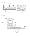
- FIG. 1 includes a schematic diagram illustrating an apparatus for manufacturing a silicon substrate manufactured according to RGS technique for directly manufacturing a silicon substrate from molten silicon in a horizontal direction and a diagram illustrating a fine structure of the silicon substrate fabricated according to the RGS technique.
- the RGS technique a latent heat of the molten silicon moving via a lower substrate 1 is removed rapidly, to manufacture a silicon substrate.
- Such the RGS technique has high productivity, compared with other methods for directly manufacturing the silicon substrate.
- a crystalline growth direction of the silicon substrate is perpendicular to a direction of moving the silicon substrate. Accordingly, grains happen to grow within the thickness of the silicon substrate.
- the crystalline growth direction of silicon is perpendicular to the silicon substrate moving direction.
- grains are densely closed and solidification is performed along a solid-liquid interface such that impurities might be concentrated on a surface of the silicon substrate. Accordingly, there might be a problem of deteriorated conversion efficiency in the manufactured solar battery.
- a direction of manufacturing a silicon substrate is in parallel to a direction of crystalline growth. Accordingly, the size of a crystalline grain generated in the silicon substrate is large enough to enhance conversion efficiency.
- the conventional vertical growth technique has a problem of low productivity, because the silicon solidification speed is quite slow.
- an object of the invention is to provide an apparatus for manufacturing a silicon substrate that can make a solid-liquid interface to be perpendicular to a crystal growth direction of silicon in manufacturing a silicon substrate and that can control the grain size of silicon to be enlarged.
- Another object of the invention is to provide an apparatus for manufacturing a silicon substrate that can manufacture a silicon substrate having enhanced conversion efficiency according to a continuous casting method capable of enabling continuous production and physical control, with enhancing productivity simultaneously.
- an apparatus for manufacturing a silicon substrate includes a crucible part; a molding part extended from an outlet of the crucible part, the molding part comprising a molding space where a silicon substrate is formed; and a dummy bar inserted in the molding space from a predetermined portion of the molding part, wherein the dummy bar is formed of a single-crystalline material.
- the single-crystalline material may be single-crystalline silicon.
- the apparatus for manufacturing the silicon substrate may further include a dummy bar coupling part that is able to be coupled to the dummy bar.
- the apparatus for manufacturing the silicon substrate may further include a driving part to drive the dummy bar coupling part to be movable in a longitudinal direction of the molding part.
- the crucible part may include a top surface, side surfaces extended from the top surface in a downward direction, a bottom surface extended from the side surfaces in a perpendicular direction and an inclined part having a slope of an acute angle with respect to one of the side surfaces.
- the apparatus for manufacturing the silicon substrate may further include a closable part arranged adjacent to the molding part to cover an outside of the dummy bar coupling part, the closable part that is expandable and contractible in a longitudinal direction of the dummy bar.
- the crucible part may include a first crucible part and a second crucible part
- the first crucible part may include a top surface, side surfaces extended from the top surface in a downward direction, a bottom surface extended from the side surfaces in a perpendicular direction and a first outlet formed through a predetermined portion thereof in a parallel direction with respect to the bottom surface
- the second crucible part may be insertedly coupled to the first crucible part and the second crucible part may include a second inclined part connected with the bottom surface, with a slope of an acute angle with respect to an upper portion of the top surface provided in the first crucible part.
- the apparatus for manufacturing the silicon substrate may further include a main chamber to provide an airtight space, wherein the crucible part comprises a raw material injecting part provided in the main chamber, having a raw material injecting hole passing through an upper portion thereof, and a gas injecting part spaced apart a predetermined distance from the raw material injecting hole, having a gas injecting hole passing through an upper portion thereof; a raw material supplying part comprising a raw material supplying body arranged on the main chamber to store a silicon raw material, a raw material supplying pipe to connect the raw material supplying body and the raw material injecting part with each other and a first valve to control opening and closing of the raw material supplying pipe; and a gas supplying part to supply an inert gas to the crucible part.
- an apparatus for manufacturing a silicon substrate includes a crucible part to form molten silicon therein, the crucible part comprising an outlet formed through a predetermined portion thereof in a parallel direction with respect to a bottom surface thereof; a molding part extended from the outlet in a parallel direction with respect to the outlet of the crucible part, the molding part comprising a molding space where a silicon substrate is formed; and a dummy bar inserted in the molding part, wherein the dummy bar is formed of single-crystalline to enable a solid-liquid interface generated in forming the silicon substrate to be substantially perpendicular to a direction in which the silicon substrate is formed.
- the apparatus for manufacturing the silicon substrate may further include a dummy bar coupling part that is able to be coupled to the dummy bar.
- the crucible part may include a top surface, side surfaces extended from the top surface in a downward direction and an inclined part having a slope of an acute angle with respect to one of the side surfaces.
- the apparatus for manufacturing the silicon substrate may further include a closable part to close the dummy bar and an outside of the dummy bar coupling part to prevent fluidal molten silicon from contacting with external air in the molding space.
- the crucible part may include a first crucible part and a second crucible part, and the crucible part has an inlet to charge a silicon raw material therein and a first outlet formed through a predetermined portion thereof in a parallel direction with respect to the bottom surface, and the second crucible part may have a corresponding appearance to the first crucible part, with being insertedly coupled to the first crucible part, and an internal cross section area of the second crucible part may be gradually decreased in a downward direction.
- the crucible part may include an injecting hole passing through an upper portion of the crucible part, and the crucible part may further include a raw material supplying part to supply a silicon raw material to the injecting part; and a gas supplying part to supply gas to the injecting part, and the silicon raw material and the gas is selectively supplied to the injecting part.
- an apparatus for manufacturing the silicon substrate includes a crucible part comprising an outlet formed through a predetermined portion thereof in a parallel direction with respect to a bottom surface thereof; a molding part extended from the outlet in a parallel with respect to the outlet of the crucible part, the molding part comprising a molding space where a silicon substrate is formed; and a dummy bar inserted in the molding space from a predetermined portion of the molding part, wherein an end of the dummy bar is formed of a single-crystalline material.
- the ingle-crystalline material may be single-crystalline silicon.
- an apparatus for manufacturing the silicon substrate includes a crucible part to accommodate molten silicon; a molding part physically connected with the crucible part, to form a silicon substrate; and a dummy bar having a single-crystalline material to align grains of a silicon substrate in a single direction, when a silicon substrate is formed in the molding part.
- the single direction of the aligned grains of the silicon substrate formed in the molding part may be a longitudinal direction of the molding part.
- the embodiments have following advantageous effects.
- the silicon substrate is formed by using the single-crystalline dummy bar, different from the conventional silicon substrate manufacturing apparatus including a lower substrate that removes a latent heat of molten silicon to solidify the molten silicon in a molding part via a crucible part. Accordingly, the size of the grains generated in the silicon substrate may be enlarged.
- the single-crystalline dummy bar inserted in the molding part is used. Accordingly, the growth direction of the silicon grains and the solid-liquid interface may be perpendicular to each other, to enlarge the size of the grains in the silicon substrate.
- the silicon substrate is pulled horizontally. Accordingly, productivity may be enhanced.
- FIG. 1 includes a schematic diagram illustrating an apparatus for manufacturing a silicon substrate manufactured according to RGS technique for directly manufacturing a silicon substrate from molten silicon in a horizontal direction and a diagram illustrating a fine structure of the silicon substrate fabricated according to the RGS technique;
- FIG. 2 is a diagram schematically illustrating an apparatus for manufacturing a silicon substrate according to an embodiment of the invention
- FIG. 3 is a perspective view illustrating a crucible part shown in FIG. 2 ;
- FIG. 4 is a sectional view illustrating an apparatus for manufacturing a silicon substrate according to another embodiment of the invention.
- FIG. 5 is an exploded perspective view of FIG. 4 ;
- FIG. 6 is a diagram illustrating an apparatus for manufacturing a silicon substrate according to a further embodiment of the invention.
- FIG. 7 is a diagram illustrating an apparatus for manufacturing a silicon substrate according to a still further embodiment of the invention.
- FIG. 8 is a diagram specifically illustrating the apparatus for manufacturing the silicon substrate according to the embodiment.
- FIG. 9 is a sectional view illustrating a molding part shown in FIG. 8 ;
- FIG. 10 is a diagram schematically illustrating an apparatus for manufacturing a silicon substrate according to a still further embodiment of the invention.
- FIG. 11 is a diagram schematically illustrating a moving direction of a dummy bar shown in FIG. 10 and a grain of the silicon substrate;
- FIG. 12 is a diagram a diagram illustrating an apparatus for manufacturing a silicon substrate according to a still further embodiment of the invention.
- FIG. 13 is a diagram a diagram illustrating an apparatus for manufacturing a silicon substrate according to a further embodiment of the invention.
- FIG. 14 is a diagram illustrating a closable part shown in FIG. 13 that is unfolded.
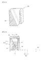
- FIG. 2 is a diagram schematically illustrating an apparatus for manufacturing a silicon substrate according to an embodiment of the invention.
- FIG. 3 is a perspective view illustrating a crucible part shown in FIG. 2 .
- an apparatus for manufacturing a silicon substrate includes a crucible part 200 and a molding part 300.
- the crucible part 200 includes a top surface 210, side surfaces 250 and an inclined part 241.
- the crucible part 200 may be defined by the top surface 210, the side surfaces 250 downwardly extended from the top surface 210 and the inclined part 241 having a slope of an acute angle with respect to one of the side surfaces 250.
- the crucible part 200 may be formed of graphite.
- an internal cross sectional area of the crucible part 200 may be gradually decreased in a downward direction.
- the inclined part 241 may be longer in a downward direction than a side surface 250 located in opposite. Accordingly, a groove does not have to be formed in the crucible part 200 coupled to the molding part, which will be described later, to exhaust molten silicon.
- the inclined part 241 may be integrally or independently formed with the side surface 250.
- the crucible part may be defined by the top surface 210, the side surfaces 250 extended from the top surface 210 in a downward direction and a bottom surface extended from the side surfaces 250 in a perpendicular direction.
- the crucible part may provide a closed internal space.
- an inclined part is connected with the bottom surface, with a slope of an acute angle with respect to one of the side surfaces 250.
- silicon carbide (SiC) or silicon nitride (Si3N4) may be coated on an internal space of the crucible part 200. Accordingly, when the crucible part 200 is formed of graphite, contamination of silicon molten (M) may be prevented that might be caused by the graphite of the crucible part.
- the molding part 300 includes a first molding part 311 and a second molding part 321.
- the first molding part 311 may be extended from the side surface 250 facing the inclined part 241 in a perpendicular direction.
- the second molding part 321 is coupled to the inclined part 241, extended in parallel to the first molding part 311.
- the inclined part 241 and the second molding part 321 are coupled to each other by a bolt.
- the second molding part 321 may be employed as a bottom of the crucible part 200.
- a molding space is formed between the first molding part 311 and the second molding part 321.
- first molding part 311 and the second molding part 321 may form an outlet 232 to suck the molten silicon (M) stored in the crucible part 200.
- a predetermined area of an upper surface adjacent to an end of the first molding part 311 may be in contact with an end of the side surface 250 facing the inclined part.
- the internal space of the molding part 300 When the internal space of the molding part 300 is pressed at a high pressure than the internal space of the crucible part 200 by the molten silicon (M) is drawn into the molding space via the outlet 232, the internal space of the molding part may prevent the molten silicon (M) from flowing out, compared with the end of the first molding part 311 in contact with an outer surface of the side surface 250.
- the end of the inclined part 241 may be in contact with an extended line in a perpendicular direction with respect to the side surface 250 facing the inclined part 241.
- the molten silicon (M) when the molten silicon (M) is not stored in the crucible part 200 continuously, the molten silicon (M) may be prevented from remaining in the crucible part 200.
- the molten silicon (M) is transported to the molding part 300 via the outlet 232.
- the fluidal silicon molten (M) may be solidified in the molding part 232, to be a silicon substrate.
- the silicon substrate manufacturing apparatus may further include a dummy bar 400.
- An end of the dummy bar 400 is in contact with the molten silicon (M) to solidify the molten silicon (M).
- the silicon substrate manufacturing apparatus may solidify the molten silicon (M), without the dummy bar 400.
- the molten silicon (M) inside the crucible part 200 may press the molten silicon (M) located in a lower area of the crucible part 200 adjacent to the outlet 232 along the inclined part 240.
- the molten silicon (M) is pressed toward the lower area of the crucible part having the inclined part and is can move toward the outlet 232 smoothly.
- the silicon substrate manufacturing apparatus includes the inclined part 240 formed in the crucible part 200 to make the cross section area inside the crucible part decreased in the downward direction, such that the molten silicon may press the lower area of the crucible part.
- FIG. 4 is a sectional view illustrating a silicon substrate manufacturing apparatus according to another embodiment of the invention.
- FIG. 5 is an exploded perspective view of a crucible part shown in FIG. 4 .
- a silicon substrate manufacturing apparatus is similar to the apparatus according to the embodiment shown in FIG. 3 and the description of the same component elements thereof will be omitted accordingly.
- a crucible part 202 applied to this embodiment includes a first crucible part 203 and a second crucible part 204.
- the first crucible part 203 may be defined by an upper surface 210, side surfaces 250 extended from the upper surface 210 and a first inclined part 241 having a slope of an acute angle with respect to one of the side surfaces 250. Different from the crucible part 200 according to the embodiment mentioned above, the first crucible part 203 may have the inclined part.
- the first crucible part 203 may be formed of graphite.
- the second crucible part 204 may be provided in the first crucible part 203 and it may have a second inclined part 245 corresponding to the first inclined part 241.
- a crucible part 300 according to this embodiment is identical to the crucible part provided in the silicon substrate manufacturing apparatus according to the embodiment mentioned above and detailed description thereof will be omitted.
- An end of the second inclined part 245 may be in contact with a line extended in a perpendicular direction with respect to the side surface 250 facing the second inclined part 245.
- molten silicon (M) may be prevented from remaining inside the crucible part 200 if molten silicon (M) is not stored in the crucible part 200 continuously.
- the second inclined part 245 of the second crucible part may be longer than the side surface 250 facing the second inclined part in a downward direction.
- the second crucible part 204 may be formed of quartz and the material used for the second crucible may not be limited thereto.
- the second crucible part 204 may be formed of any materials capable of preventing the molten silicon from being contaminated by the first crucible part 203.
- SiC or Ni3N4 may be coated on the first crucible part 203.
- the second crucible part 204 is a quartz crucible, graphite and quartz physically contact with each other only to prevent SiO or Co gas from being generated from an interface.
- a cross section area inside the second crucible part 203 may be gradually decreased in a downward direction.
- the crucible part 202 applied to the silicon substrate manufacturing apparatus includes the second crucible part 204 capable of shutting off carbon from penetrating into the molten silicon (M), when the first crucible part 203 is a graphite crucible. Accordingly, contamination of the molten silicon (M) can be prevented.
- the second crucible part may have the inclined internal structure, although the first crucible part has no inclined structure. Accordingly, the molten silicon may move via the outlet smoothly.
- FIG. 6 is a diagram illustrating a silicon substrate manufacturing apparatus according to a further embodiment of the invention.
- the silicon substrate manufacturing apparatus includes a main chamber 100, a crucible part 200, a raw material supplying part 500 and a gas supplying part 600.
- the main chamber 100 provides an airtight closable space and it is closable at a predetermined side although not shown in the drawing.
- the crucible part 200 may be one of the crucible parts described in the embodiments mentioned above and it may include a raw material injecting part 212 and a gas injection part 214.
- the raw material injection part 212 may include a raw material injecting hole 211 passing through a top of the crucible part.
- the gas injecting part 214 may include a gas injecting hole 213 passing through the top of the crucible part 200, spaced apart a predetermined distance from the raw material injecting hole.
- the raw material supplying part 500 may include a raw material supplying body 502, a raw material supplying pipe 504 and a first valve 506.
- the raw material body 502 may be arranged on the main chamber 100 to store silicon raw material such that a predetermined amount of silicon raw material may be exhausted via an outlet formed through a bottom surface of the raw material body 502 regularly.
- the raw material supplying pipe 504 passes through a top surface of the main chamber 100 to connect a bottom of the raw material supplying body 502 and the raw material injection part 212 of the crucible part 200 with each other, such that the silicon raw material exhausted from the raw material supplying body 502 may be supplied to the internal space of the crucible part 200.
- the first valve 506 may be arranged between the raw material supplying body 502 and the raw material supplying pipe 504. Also, the first valve 506 may be arranged on the main chamber 100 and it may be distant from the crucible part, to prevent damage generated by the heat.
- the first valve 506 when the silicon raw material is supplied to the crucible part 200, the first valve 506 is open. When an inert gas is supplied from the top of the main chamber 100, the first valve 506 is closed. Accordingly, the inert gas may not be detained in the raw material supplying body 502 via the raw material supplying pipe 504.
- the gas supplying part 600 may include a gas generator 602, a gas supplying pipe 604 and a second valve 606.
- the gas generator 602 may generate an inert gas having a low reactivity with graphite such as argon (Ar) or it may provide a predetermined space to store the inert gas.
- the gas supplying pipe 604 may passes through the top of the main chamber 100 to connect the gas generator 602 and the gas injecting part 214 of the crucible part with each other, to supply the inert gas to the crucible part 200 from the gas generator 602.
- the gas supplying part may not include the gas supplying pipe.
- an internal space of the main chamber 100 is pressed by the inert gas supplied from the gas generator 602 and the inert gas is supplied from the main chamber 100 via the gas injecting part 214, such that an entire space inside both of the main chamber and the crucible part 200 may be pressed by the inert gas.
- the inert gas may press the internal space of the crucible part 200 to exhaust the molten silicon (M) via the outlet 232 shown in FIG. 2 smoothly.
- the internal pressure of the crucible part 200 enabled by the inert gas may be 1 ⁇ 5 bar to exhaust the molten silicon (M) via the outlet 232, when the fluidity of the molten silicon is deteriorated too much, and to prevent a pore from being generated in the molten silicon (M) by the high pressure of the inert gas.
- the second valve 606 may be arranged between the gas generator 602 and the gas supplying pipe 604.
- the second valve 606 may be arranged on the main chamber 100.
- the first valve When the inert gas is supplied to the crucible part 200, the first valve is closed and the second valve is open.
- the first valve 506 is closed to prevent the inert gas from pressing the inside of the raw material supplying body 502 after drawn therein.
- the silicon substrate manufacturing apparatus can prevent the manufacture cost of the raw material body 502 from increasing to have the material or structure that enables the raw material supplying body 502 to endure the pressed inert gas.
- FIG. 7 is a diagram illustrating a silicon substrate manufacturing apparatus according to a still further embodiment of the invention.
- the silicon substrate manufacturing apparatus includes a main chamber 100, an auxiliary chamber 110, a crucible part 200, a raw material supplying part 501 and a gas supplying part 601.
- the main chamber 100 provides an airtight space and it is closable at a predetermined side.
- the crucible part 200 may be similar to one of the embodiments mentioned above.
- the crucible part 200 according to this embodiment includes a single injecting part 215 to inject the silicon raw material and the inert gas there through, without the raw material injecting part and the gas injecting part 214 mentioned above independently.
- the raw material supplying part 501 may include a raw material supplying body 510 and a supplying pipe 550.
- the raw material supplying body 510 may be installed in the auxiliary chamber 110 and it includes a raw material storing part 512 and a raw material moving part 514.
- the raw material storing part 512 provides a predetermined space to store the silicon raw material (P).
- the raw material moving part 514 may be connected with the raw material storing part 512 and it may move a predetermined amount of silicon raw material (P) regularly.
- the supplying pipe 550 is connected with the injecting part 215 of the crucible part, adjacent to an end of the raw material moving part 514.
- the supplying pipe 550 includes a first supplying pipe 552 and a second supplying pipe 554.
- the first supplying pipe 552 may define a lower part of the raw material supplying pipe 550 and it may be arranged in the main chamber 100.
- the first supplying pipe 552 may be formed of graphite and it may prevent the raw material from being damaged by the heat in the high temperature chamber 100.
- the second supplying pipe 554 may define an upper part of the raw material supplying pipe 550 and it may be arranged in the auxiliary chamber 110.
- the second supplying pipe 554 is formed of stainless steel.
- the material used for the second supplying pipe 554 is not limited thereto and it may be any metal that is able to endure the heat inside of the auxiliary chamber 110, with high anticorrosion.
- the supplying pipe 550 may further include a supplying part upper end 556 extended from the second supplying pipe 554, with a cross sectional area gradually increasing in an upward direction.
- the silicon raw material (P) moved to the raw material moving part 514 may be supplied to the supplying pipe 550 smoothly.
- the gas supplying part 601 may be provided adjacent to the auxiliary chamber 110 and it may generate an inert gas or provide a predetermined space to store the inert gas.
- auxiliary chamber 110 may have a hole formed there through to receive the inert gas from the gas supplying part 601.
- the inert gas When the inert gas is supplied to the auxiliary chamber 110 from the gas supplying part 601, the inert gas may press an internal space of the auxiliary chamber 110 and the crucible part 200 via the supplying pipe 550 simultaneously.
- the auxiliary chamber 110 and the raw material supplying part 501 may be formed of a predetermined material capable of enduring the pressure generated by the inert gas.
- the silicon substrate manufacturing apparatus may selectively supply the silicon raw material and the inert gas to the crucible part 200 via the single supplying pipe 550, different from the silicon substrate manufacturing apparatus according to the embodiment shown in FIG. 6 .
- the silicon raw material and the inert gas are supplied via the single supplying pipe 550 and the manufacturing cost can be lowered, compared with the raw material supplying pipe and the gas supplying pipe separately provided as shown in FIG. 6 .
- the supplying pipe capable of enduring the high temperature is united to reduce the manufacturing cost.
- auxiliary chamber 110 Only the auxiliary chamber 110 is pressed, not the entire part of the main chamber 100, to reduce the unnecessary inert gas supply.
- the opening and closing of the valve is not complicated and the silicon substrate manufacturing apparatus can be operated smoothly.
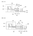
- FIG. 8 is a diagram specifically illustrating the silicon substrate manufacturing apparatus the according to the embodiment shown in the first embodiment and FIG. 9 is a sectional view illustrating the molding part shown in FIG. 8 .
- the silicon substrate manufacturing apparatus includes the crucible part 200, a heating part 610, the molding part 300, a cooling part 640 and a transporting part 670.
- the crucible part 200 is described in reference to FIG. 2 and detailed description thereof will be omitted.
- the heating part 610 may be installed outer to the crucible part 200.
- the heating part 610 may heat the crucible part 200 and it may melt the silicon raw material charged in the crucible part 200, to form the molten silicon (M).
- the heating part 610 may maintain the temperature of the molten silicon (M), when the molten silicon (M) is directly supplied to the crucible part 200.
- the heating part 610 includes a first heating part 612 arranged along an outside of the side surface 250 constituting the crucible part and a second heating part 614 arranged along an outside of the bottom surface 230 constituting the crucible part.
- the first heating part 612, the second heating part 614 and a third heating part 260 may have a heater and an induction coil.
- the first heating part 612 and the second heating part 614 may be controlled independently and a temperature difference of the molten silicon (M) inside the crucible part 200 may be reduced accordingly.
- the temperature of the molten silicon (M) may be 1300 ⁇ 1500°C to prevent solidification of the molten silicon (M) within the crucible part 200 and to prevent increase of the cost taken to heat the molten silicon (M) to maintain the temperature.
- the molding part 300 may be extended from the outlet 232 in a parallel direction with respect to the outlet 232 of the crucible part and it may have a molding space where the silicon substrate (S) is formed.
- the molding part 300 may include an auxiliary heating part 615 to control the temperature for solidifying the silicon substrate (S) inside the molding space.
- the molding space may be divided into a solidification region (S1) to cool and solidify the silicon substrate (S) and a stress releasing region (S2) to release stress remaining in the solidified silicon substrate (S).
- S1 solidification region
- S2 stress releasing region
- the solidification region (S1) starts at an area of the molding part 300 adjacent to the outlet 232 to an area in front of the molding part 300 in a moving direction of the silicon substrate (S).
- the molten silicon (M) supplied from the outlet 232 may be solidified primarily. Although not shown in the drawing, a straight distance between both ends of the solidification region (S1) may be longer than a straight distance between both ends of the outlet 232.
- the stress releasing region (S2) starts at an area adjacent to the solidification region (S1) to an area behind the molding part 300.
- the silicon substrate (S) may be annealed secondarily to release the stress of the silicon substrate (S) and to prevent the solidified substrate from rapidly being cooled.
- the auxiliary heating part 615 may include a first auxiliary heating part 616 and a second auxiliary heating part 617.
- the first auxiliary heating part 616 may be installed corresponding to the solidification region (S1) and it may primarily heat the silicon substrate (S) located in the solidification region (S1).
- the second auxiliary heating part 617 may be installed corresponding to the stress releasing region (S2) and it may heat the silicon substrate (S) located in the stress releasing region (S2).
- the first auxiliary heating part 616 or the second auxiliary heating part 617 may have a heater or an induction coil.
- the first and second auxiliary heating parts 616 and 617 may be installed outer to the molding part 300.
- the position of the molding part is not limited thereto and the molding part 300 may be installed in the molding part.
- the size of the grain generated in the silicon substrate (S) might be smaller than the required size or the remaining stress might be enlarged.
- the first auxiliary heating temperature achieved by the first auxiliary heating part 616 may be the silicon melting temperature or higher and the second auxiliary heating temperature achieved by the second auxiliary heating part 617 may be lower than the silicon melting temperature.
- the temperature at which the silicon substrate is solidified may be controlled by the auxiliary heating part 615 and the grain size of the silicon substrate may be enlarged accordingly, to prevent the stress fro remaining.
- the cooling part 640 may be installed at a rear end of the molding part 300. Also, the cooling part 640 may cool the silicon substrate (S) molded in the molding part 300 below 200°C.
- the transporting part 670 may be installed behind the molding part 300 and it may move the silicon substrate (S) solidified in the molding part 300 in a horizontal direction.
- the transporting part 670 may have a pair of transfer rollers 672 and 674 rotated in a reverse direction.
- the transfer speed of the silicon substrate (S) transferred by the transfer rollers 672 and 674 may be identical to the silicon solidifying speed.
- the transfer speed of the silicon substrate transferred by the transfer part 670 may affect the thickness of the silicon substrate and it may be 10 cm/min or less.
- FIG. is a diagram schematically illustrating a silicon substrate manufacturing apparatus according to a still further embodiment of the invention.
- FIG. 11 is a diagram schematically illustrating a moving direction of a dummy bar shown in FIG. 10 and a grain of the silicon substrate.
- the silicon substrate manufacturing apparatus is similar to the silicon substrate manufacturing apparatus described in reference to FIG. 2 and description of the same component elements will be omitted accordingly.
- the silicon substrate manufacturing apparatus may further include a dummy bar 400, different from the apparatus described in reference to FIG. 8 .
- the dummy bar 400 may be inserted in the molding space of the molding part 300 from an end at which the silicon substrate (S) formed in the molding space of the molding part 300 is moved.
- the dummy bar 400 may be formed of a single-crystalline material.
- the single-crystalline material may be single crystalline silicon or single-crystalline germanium.
- the dummy bar 400 may be formed of graphite and the single-crystalline material is bonded to an end of the dummy bar 400.
- the dummy bar 400 may have a corresponding shape with respect to the molding space of the molding part 300.
- the dummy bar 400 may be inserted in the molding space of the molding part 300 and the molten silicon (M) formed in the crucible part 200 may contact with an end of the dummy bar 400.
- the growth direction (B) of the grains generated in the silicon substrate formed by surface-contacting the molten silicon from the end of the dummy bar 400 may be substantially perpendicular to the end of the dummy bar.
- a solid-liquid interface between the liquid molten silicon and the silicon substrate may be perpendicular to the growth direction of the silicon grains.
- the dummy bar 400 formed of single-crystalline may enable the grains of the single-crystalline silicon aligned in a single direction, compared with the dummy bar formed of polycrystalline silicon, such that the grains of the silicon substrate may be enlarged.
- the single direction in which the grains of the silicon substrate formed in the molding part 300 are aligned may be a longitudinal direction of the molding part.
- the silicon substrate manufacturing apparatus uses the dummy bar formed of the single-crystalline material. Accordingly, the manufactured silicon substrate may enlarge the grains of the silicon, compared with the grains of the silicon according to the conventional RGS method.
- the fabricated silicon substrate may be moved upwardly and there is a problem of a long time taken to manufacture the silicon substrate.
- the silicon substrate manufacturing substrate according to this embodiment may enable the crystalline growth direction of the silicon and the solid-liquid interface to be maintained in vertical direction and it may enhance productivity, compared with the conventional silicon substrate manufacturing apparatus according to the direct manufacturing method.
- the grain size of the silicon may be enlarged and the silicon substrate productivity may be enhanced simultaneously.
- the crucible part 200 may include a top surface 210, side surfaces 250 extended from the top surface 210 in a downward direction and an inclined part 241 having a slope of an acute angle with respect to one of the side surfaces 250.
- the molten silicon is flowing into the molding space along the inclined part 241 of the crucible part and the silicon substrate can be manufactured by the dummy bar, without a structure provided in the bottom surface of the molding or the crucible part to transfer the silicon substrate.
- the crucible part 202 may include the first crucible part 203 and the second crucible part 203 having the second inclined part 245.
- the second crucible part 245 has the second inclined part 245 to enable the silicon substrate to be formed by using the dummy bar, without the structure provided in the bottom surface of the crucible part or the molding part to transfer the silicon substrate.
- FIG. 12 is a diagram illustrating a silicon substrate manufacturing apparatus according to a still further embodiment.
- the silicon substrate manufacturing apparatus according to this embodiment is similar to the silicon substrate manufacturing apparatus according to the embodiment described in reference to FIG. 10 and detailed description of the same component elements will be omitted.
- the silicon substrate manufacturing apparatus includes a crucible part 200, a molding part 302, a dummy bar 400 and a cooling part 650.
- the crucible part 200 may have an outlet 232 formed through a predetermined portion of the crucible part 200, in parallel to the bottom surface thereof.
- the crucible part 200 may include a top surface 210, side surfaces 250 extended from the top surface 210 in a downward direction and an inclined part 241 having a slope of an acute angle with respect to one of the side surfaces 250.
- the molding part 302 may be extended from the outlet 232 in a parallel direction with respect to the outlet 232 of the crucible part and it may have a molding space in which the silicon substrate is formed.
- the molding part 302 may include a first molding part 315 extended from a side surface 250 facing the inclined part 241 in a perpendicular direction and a second molding part 325 coupled to the inclined part 241, extended in a parallel to the first molding part 315.
- the first molding part 315 may be shorter than the second molding part 325 with respect to the outlet 232.
- the first molding part 315 may not be positioned in a predetermined area of the region in which the molten silicon is converted into the silicon substrate.
- an upper area of the molding space may be partially exposed.
- the dummy bar 400 may be inserted in the molding space from a predetermined portion of the molding part 302.
- the cooling part 650 may be installed adjacent to the molding part.
- the cooling part 650 may include a gas blowing part to blow gas.
- the gas blowing part may blow gas toward the area having no first molding part 315 toward the molding space.
- the gas may be an inert gas and the inert gas may be helium, argon or nitrogen or a mixture of them.
- the cooling part may not be limited thereto and it may have a mechanism having a cooling channel.
- the silicon substrate manufacturing apparatus may cool the dummy bar or the silicon substrate via an upper portion of the molding part, when the silicon substrate is formed in the molding space.
- the cooling part 650 blow the gas toward the dummy bar or silicon substrate partially exposed from the molding part to cool the silicon substrate.
- the silicon substrate manufacturing apparatus has an advantage of no dummy bar coupling part or auxiliary cooling device provided at an end of the molding part.
- air cooling may be performed, rather than water cooling, to reduce the cooling cost.
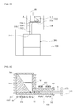
- FIG. 13 is a diagram illustrating a silicon substrate manufacturing apparatus according to a still further embodiment.
- the silicon substrate manufacturing apparatus further include a dummy bar coupling part 700, a moving part 800 and a closable part 900, different from the apparatus according to the embodiment described in reference to FIG. 11 .
- the dummy bar coupling part 700 may be coupled to the dummy bar 400 and it may be formed of graphite.
- the dummy bar coupling part 700 and the dummy bar may be coupled to each other by a bolt.
- the dummy bar coupling part 700 may have a clamp shape.
- the dummy bar coupling part 700 may include a coupling body 710, an upper coupling portion 720 that is able to surface-contact with an upper surface of the dummy bar and a lower coupling portion 740 that is able to surface-contact with a lower surface of the dummy bar 400, in parallel to the upper coupling portion.
- the upper coupling portion 720 and the lower coupling portion 740 may be formed of a predetermined material having elasticity.
- the upper coupling portion 720 and the lower coupling portion 740 may prevent the shock applied to the dummy bar 400 when they are in surface-contact with the dummy bar 400.
- the upper coupling portion 720 and the lower coupling portion 740 presses the dummy bar 400 in an up-and-down direction, such that the dummy bar coupling part 700 may be coupled to the dummy bar 400.
- the dummy bar coupling part 700 may have a cooling channel.
- a fluidal material flows via the cooling channel in the dummy coupling part 700, to lower the temperature of the dummy coupling part 700 and to lower the temperature of the dummy bar 400 coupled to the dummy coupling part 700 accordingly.
- the temperature of the dummy bar 400 may be lowered and a latent heat of the molten silicon within the molding part may be removed, to solidify the silicon substrate.
- the cooling channel is provided in the dummy bar coupling part 700 and an unnecessary heat can be removed, only to prevent the neighboring graphite from contaminating the silicon substrate.
- the moving part 800 may be connected with the dummy bar coupling part 700, to move the dummy bar coupling part 700 horizontally.
- the moving part 800 includes a moving body 810, a moving support 820 and a driving part 840.
- the moving body 810 is connected with the dummy bar coupling part 700.
- the moving support 820 may support the moving body 810 and it may have a rail 822. Although not shown in the drawing, the moving body 810 may have a wheel corresponding to the rail 822.
- the moving support 820 may have all types of mechanisms enabling the moving support to move the moving body, not limited to the rail 822.
- the driving part 840 is installed in the moving body 810 and it provides a rotational force to the wheel.
- the wheel rotatable by the driving part 840 may be rotated along the rail 822.
- the moving part 800 may be moved horizontally to insert the dummy bar 400 coupled to the dummy bar coupling part 700 in the molding part 300 or withdraw it from the molding part 300.
- the dummy bar coupling part 700 and the moving part 800 that consists of the mechanism capable of pulling the dummy bar are provided in the silicon substrate manufacturing apparatus according to this embodiment such that damage to the molded silicon substrate caused by the roller may be prevented.
- the silicon substrate manufacturing apparatus may further include a main chamber 100 to accommodate the crucible part 200 and the molding part 300.
- the closable part 900 may be next to the main chamber 100 and it may cover an outer portion of the dummy bar coupling part 700, expandable in a longitudinal direction of the dummy bar 400.
- the closable part 900 may be a bellows as shown in FIG. 13 .
- the closable part 900 may be formed of stainless steel or aluminum alloy.
- the stainless steel may be an alloyed steel of iron and chrome or an alloyed steel of iron, nickel and chrome.
- the material used for the closable part is not limited to the stainless steel or aluminum alloy and it may be a metallic material capable of enduring the heat generated from the side of the molding part 300, with high corrosion resistance.
- the closable part 900 may have an expandable part 910 and a connecting part 920.
- the expandable part 910 may be expandable as far as the dummy bar coupling part 700 is movable horizontally on the moving support 820. Accordingly, the expandable part 910 may be expanded or contracted, corresponding to the horizontal movement of the dummy bar coupling part 700, such that external air may be prevented from coming into the expandable part 910.
- the connecting part 920 may include a first connecting part 922 to connect the main chamber 100 and the expandable part 910 with each other and a second connecting part 924 to connect the moving part 800 and the expandable part 910 with each other.
- the first connecting part 922 or the second connecting part 924 may have a groove corresponding to a bolt enabling bolt fastening.
- the closable part 900 may be coupled to or separated from the portion of the main chamber 100 or the moving part 800 when necessary.
- the closable part 900 may enable the dummy bar coupling part 700 to be arranged in the airtight space.
- the silicon substrate manufacturing apparatus may include the closable part 900 installed outer to the dummy bar coupling part 700. Accordingly, the dummy bar coupling part formed of graphite may be prevented from being oxidized after contacting with external air.
Landscapes
- Chemical & Material Sciences (AREA)
- Engineering & Computer Science (AREA)
- Organic Chemistry (AREA)
- Crystallography & Structural Chemistry (AREA)
- Materials Engineering (AREA)
- Metallurgy (AREA)
- Condensed Matter Physics & Semiconductors (AREA)
- Physics & Mathematics (AREA)
- Mechanical Engineering (AREA)
- Electromagnetism (AREA)
- General Physics & Mathematics (AREA)
- Computer Hardware Design (AREA)
- Microelectronics & Electronic Packaging (AREA)
- Power Engineering (AREA)
- Inorganic Chemistry (AREA)
- Silicon Compounds (AREA)
- Crystals, And After-Treatments Of Crystals (AREA)
Abstract
Description
- [TECHNICAL FIELD]
- Embodiments may relate to an apparatus for manufacturing a silicon substrate, more particularly, to an apparatus for manufacturing a silicon substrate for a solar battery, using continuous casting.
- [BACKGROUND]
- Generally, silicon is molted and molten silicon is solidified to fabricate a single-crystalline silicon ingot or polycrystalline silicon block. The single-crystalline silicon ingot or polycrystalline silicon block is cut and a silicon substrate is manufactured.
- The single-crystalline silicon ingot is fabricated according to Czochralski method through a crystalline growth process using seed crystals from silicon molten.
- The polycrystalline block is fabricated through a single-direction solidification process according to Heat Exchanger (HEM) or Bridman-Stockbarger method.
- The fabricated single-crystalline silicon Ingot or polycrystalline silicon block is manufactured into a silicon substrate through various cutting processes.
- During the cutting process of the single-crystalline ingot or polycrystalline silicon block, 40∼50% of Kerf-loss might be generated. Accordingly, there is a disadvantage of increased production cost for a silicon substrate for a solar battery that is caused by the Kerf-loss generated during the process of manufacturing the silicon substrate.
- To solve the disadvantage there have been active studies on a method of directly manufacturing a thin silicon substrate from molten silicon, without the ingot cutting process.
- Currently, direct manufacturing technique with respect to a silicon substrate for a solar battery can be categorized into a vertical growth technique and a horizontal growth technique. A conventional vertical growth technique includes edge-defined film-fed growth (EFG), string ribbon (SR). The horizontal growth technique includes ribbon growth on substrate (RGS) and crystallization on dipped substrate (CDS).
-
FIG. 1 includes a schematic diagram illustrating an apparatus for manufacturing a silicon substrate manufactured according to RGS technique for directly manufacturing a silicon substrate from molten silicon in a horizontal direction and a diagram illustrating a fine structure of the silicon substrate fabricated according to the RGS technique. - In the RGS technique, a latent heat of the molten silicon moving via a
lower substrate 1 is removed rapidly, to manufacture a silicon substrate. Such the RGS technique has high productivity, compared with other methods for directly manufacturing the silicon substrate. However, if manufacturing the silicon substrate according to the RGS method, a crystalline growth direction of the silicon substrate is perpendicular to a direction of moving the silicon substrate. Accordingly, grains happen to grow within the thickness of the silicon substrate. - Also, as shown in
FIG. 1 (a) , the crystalline growth direction of silicon is perpendicular to the silicon substrate moving direction. As shown inFIG. 1 (b) , grains are densely closed and solidification is performed along a solid-liquid interface such that impurities might be concentrated on a surface of the silicon substrate. Accordingly, there might be a problem of deteriorated conversion efficiency in the manufactured solar battery. - Meanwhile, in a conventional vertical growth technique, a direction of manufacturing a silicon substrate is in parallel to a direction of crystalline growth. Accordingly, the size of a crystalline grain generated in the silicon substrate is large enough to enhance conversion efficiency. However, the conventional vertical growth technique has a problem of low productivity, because the silicon solidification speed is quite slow.
- In the conventional direct manufacturing technique with respect to a silicon substrate, silicon substrate productivity and energy conversion efficiency are in trade-off. Accordingly, there are demands on a silicon substrate manufacturing technique that is able to enhance both productivity and quality of the silicon substrate.
- [PRIOR ART DOCUMENTS]
- Korean Registered Patent No.
10-1080757 - Japan Publicized Patent No.
1995-256624 - [DISCLOSURE]
- [TECHNICAL PROBLEM]
- To solve the problems, an object of the invention is to provide an apparatus for manufacturing a silicon substrate that can make a solid-liquid interface to be perpendicular to a crystal growth direction of silicon in manufacturing a silicon substrate and that can control the grain size of silicon to be enlarged.
- Another object of the invention is to provide an apparatus for manufacturing a silicon substrate that can manufacture a silicon substrate having enhanced conversion efficiency according to a continuous casting method capable of enabling continuous production and physical control, with enhancing productivity simultaneously.
- [TECHNICAL SOLUTION]
- In an aspect of the invention, an apparatus for manufacturing a silicon substrate includes a crucible part; a molding part extended from an outlet of the crucible part, the molding part comprising a molding space where a silicon substrate is formed; and a dummy bar inserted in the molding space from a predetermined portion of the molding part, wherein the dummy bar is formed of a single-crystalline material.
- The single-crystalline material may be single-crystalline silicon.
- The apparatus for manufacturing the silicon substrate may further include a dummy bar coupling part that is able to be coupled to the dummy bar.
- The apparatus for manufacturing the silicon substrate may further include a driving part to drive the dummy bar coupling part to be movable in a longitudinal direction of the molding part.
- The crucible part may include a top surface, side surfaces extended from the top surface in a downward direction, a bottom surface extended from the side surfaces in a perpendicular direction and an inclined part having a slope of an acute angle with respect to one of the side surfaces.
- The apparatus for manufacturing the silicon substrate may further include a closable part arranged adjacent to the molding part to cover an outside of the dummy bar coupling part, the closable part that is expandable and contractible in a longitudinal direction of the dummy bar.
- The crucible part may include a first crucible part and a second crucible part, and the first crucible part may include a top surface, side surfaces extended from the top surface in a downward direction, a bottom surface extended from the side surfaces in a perpendicular direction and a first outlet formed through a predetermined portion thereof in a parallel direction with respect to the bottom surface, and the second crucible part may be insertedly coupled to the first crucible part and the second crucible part may include a second inclined part connected with the bottom surface, with a slope of an acute angle with respect to an upper portion of the top surface provided in the first crucible part.
- The apparatus for manufacturing the silicon substrate may further include a main chamber to provide an airtight space, wherein the crucible part comprises a raw material injecting part provided in the main chamber, having a raw material injecting hole passing through an upper portion thereof, and a gas injecting part spaced apart a predetermined distance from the raw material injecting hole, having a gas injecting hole passing through an upper portion thereof; a raw material supplying part comprising a raw material supplying body arranged on the main chamber to store a silicon raw material, a raw material supplying pipe to connect the raw material supplying body and the raw material injecting part with each other and a first valve to control opening and closing of the raw material supplying pipe; and a gas supplying part to supply an inert gas to the crucible part.
- In another aspect of the invention, an apparatus for manufacturing a silicon substrate includes a crucible part to form molten silicon therein, the crucible part comprising an outlet formed through a predetermined portion thereof in a parallel direction with respect to a bottom surface thereof; a molding part extended from the outlet in a parallel direction with respect to the outlet of the crucible part, the molding part comprising a molding space where a silicon substrate is formed; and a dummy bar inserted in the molding part, wherein the dummy bar is formed of single-crystalline to enable a solid-liquid interface generated in forming the silicon substrate to be substantially perpendicular to a direction in which the silicon substrate is formed.
- The apparatus for manufacturing the silicon substrate may further include a dummy bar coupling part that is able to be coupled to the dummy bar.
- The crucible part may include a top surface, side surfaces extended from the top surface in a downward direction and an inclined part having a slope of an acute angle with respect to one of the side surfaces.
- The apparatus for manufacturing the silicon substrate may further include a closable part to close the dummy bar and an outside of the dummy bar coupling part to prevent fluidal molten silicon from contacting with external air in the molding space.
- The crucible part may include a first crucible part and a second crucible part, and the crucible part has an inlet to charge a silicon raw material therein and a first outlet formed through a predetermined portion thereof in a parallel direction with respect to the bottom surface, and the second crucible part may have a corresponding appearance to the first crucible part, with being insertedly coupled to the first crucible part, and an internal cross section area of the second crucible part may be gradually decreased in a downward direction.
- The crucible part may include an injecting hole passing through an upper portion of the crucible part, and the crucible part may further include a raw material supplying part to supply a silicon raw material to the injecting part; and a gas supplying part to supply gas to the injecting part, and the silicon raw material and the gas is selectively supplied to the injecting part.
- In a further aspect of the invention, an apparatus for manufacturing the silicon substrate includes a crucible part comprising an outlet formed through a predetermined portion thereof in a parallel direction with respect to a bottom surface thereof; a molding part extended from the outlet in a parallel with respect to the outlet of the crucible part, the molding part comprising a molding space where a silicon substrate is formed; and a dummy bar inserted in the molding space from a predetermined portion of the molding part, wherein an end of the dummy bar is formed of a single-crystalline material.
- The ingle-crystalline material may be single-crystalline silicon.
- In a still further aspect of the invention, an apparatus for manufacturing the silicon substrate includes a crucible part to accommodate molten silicon; a molding part physically connected with the crucible part, to form a silicon substrate; and a dummy bar having a single-crystalline material to align grains of a silicon substrate in a single direction, when a silicon substrate is formed in the molding part.
- The single direction of the aligned grains of the silicon substrate formed in the molding part may be a longitudinal direction of the molding part.
- [ADVANTAGEOUS EFFECTS]
- The embodiments have following advantageous effects.
- First, the silicon substrate is formed by using the single-crystalline dummy bar, different from the conventional silicon substrate manufacturing apparatus including a lower substrate that removes a latent heat of molten silicon to solidify the molten silicon in a molding part via a crucible part. Accordingly, the size of the grains generated in the silicon substrate may be enlarged.
- Second, the single-crystalline dummy bar inserted in the molding part is used. Accordingly, the growth direction of the silicon grains and the solid-liquid interface may be perpendicular to each other, to enlarge the size of the grains in the silicon substrate.
- Finally, different from the conventional direct silicon substrate manufacturing method, the silicon substrate is pulled horizontally. Accordingly, productivity may be enhanced.
- [BRIEF DESCRIPTION OF THE DRAWINGS]
- Arrangements and embodiments may be described in detail with reference to the following drawings in which like reference numerals refer to like elements and wherein:
-
FIG. 1 FIG. 1 includes a schematic diagram illustrating an apparatus for manufacturing a silicon substrate manufactured according to RGS technique for directly manufacturing a silicon substrate from molten silicon in a horizontal direction and a diagram illustrating a fine structure of the silicon substrate fabricated according to the RGS technique; -
FIG. 2 is a diagram schematically illustrating an apparatus for manufacturing a silicon substrate according to an embodiment of the invention; -
FIG. 3 is a perspective view illustrating a crucible part shown inFIG. 2 ; -
FIG. 4 is a sectional view illustrating an apparatus for manufacturing a silicon substrate according to another embodiment of the invention; -
FIG. 5 is an exploded perspective view ofFIG. 4 ; -
FIG. 6 is a diagram illustrating an apparatus for manufacturing a silicon substrate according to a further embodiment of the invention; -
FIG. 7 is a diagram illustrating an apparatus for manufacturing a silicon substrate according to a still further embodiment of the invention; -
FIG. 8 is a diagram specifically illustrating the apparatus for manufacturing the silicon substrate according to the embodiment; -
FIG. 9 is a sectional view illustrating a molding part shown inFIG. 8 ; -
FIG. 10 is a diagram schematically illustrating an apparatus for manufacturing a silicon substrate according to a still further embodiment of the invention; -
FIG. 11 is a diagram schematically illustrating a moving direction of a dummy bar shown inFIG. 10 and a grain of the silicon substrate; -
FIG. 12 is a diagram a diagram illustrating an apparatus for manufacturing a silicon substrate according to a still further embodiment of the invention; -
FIG. 13 is a diagram a diagram illustrating an apparatus for manufacturing a silicon substrate according to a further embodiment of the invention; and -
FIG. 14 is a diagram illustrating a closable part shown inFIG. 13 that is unfolded. - [BEST MODE]
- As follows, embodiments will be described in detail to be embodied by those skilled in the art to which the embodiments pertain to, in reference to the accompanying drawings. Reference may now be made in detail to specific embodiments, examples of which may be illustrated in the accompanying drawings.
- Wherever possible, same reference numbers may be used throughout the drawings to refer to the same or like parts.
- Unless specific definition, meaning of all terminology used in the present specification is identical to common meaning of terminology people skilled in the art to which the present invention pertains may understand and not intended to limit the invention. Unless meaning thereof is defined specifically, a singular expression used in the specification includes a plural form. If there is collision between definition of the terminology used in the present specification and definition of the conventional terminology, definition used in the present invention has priority. Any reference in this specification to "comprise," or "include" means that there are a characteristic, a number, a step, an operation, an element, a part or combination thereof and not exclude one or more other characteristics, numbers, steps, operations, elements, parts or combinations thereof and additional possibility.
-
FIG. 2 is a diagram schematically illustrating an apparatus for manufacturing a silicon substrate according to an embodiment of the invention.FIG. 3 is a perspective view illustrating a crucible part shown inFIG. 2 . - In reference to
FIGS. 2 and3 , an apparatus for manufacturing a silicon substrate (hereinafter, a silicon substrate manufacturing apparatus) includes acrucible part 200 and amolding part 300. - The
crucible part 200 includes atop surface 210, side surfaces 250 and aninclined part 241. - The
crucible part 200 may be defined by thetop surface 210, the side surfaces 250 downwardly extended from thetop surface 210 and theinclined part 241 having a slope of an acute angle with respect to one of the side surfaces 250. Thecrucible part 200 may be formed of graphite. - In a different aspect of the invention, an internal cross sectional area of the
crucible part 200 may be gradually decreased in a downward direction. - The
inclined part 241 may be longer in a downward direction than aside surface 250 located in opposite. Accordingly, a groove does not have to be formed in thecrucible part 200 coupled to the molding part, which will be described later, to exhaust molten silicon. - In addition, the
inclined part 241 may be integrally or independently formed with theside surface 250. - Meanwhile, different from what is shown in the drawings, the crucible part may be defined by the
top surface 210, the side surfaces 250 extended from thetop surface 210 in a downward direction and a bottom surface extended from the side surfaces 250 in a perpendicular direction. - The crucible part may provide a closed internal space.
- Also, an inclined part is connected with the bottom surface, with a slope of an acute angle with respect to one of the side surfaces 250.
- Meanwhile, silicon carbide (SiC) or silicon nitride (Si3N4) may be coated on an internal space of the
crucible part 200. Accordingly, when thecrucible part 200 is formed of graphite, contamination of silicon molten (M) may be prevented that might be caused by the graphite of the crucible part. - The
molding part 300 includes afirst molding part 311 and asecond molding part 321. - The
first molding part 311 may be extended from theside surface 250 facing theinclined part 241 in a perpendicular direction. - The
second molding part 321 is coupled to theinclined part 241, extended in parallel to thefirst molding part 311. - Although not shown in the drawings, the
inclined part 241 and thesecond molding part 321 are coupled to each other by a bolt. - Accordingly, the
second molding part 321 may be employed as a bottom of thecrucible part 200. - A molding space is formed between the
first molding part 311 and thesecond molding part 321. - Also, the
first molding part 311 and thesecond molding part 321 may form anoutlet 232 to suck the molten silicon (M) stored in thecrucible part 200. - A predetermined area of an upper surface adjacent to an end of the
first molding part 311 may be in contact with an end of theside surface 250 facing the inclined part. - When the internal space of the
molding part 300 is pressed at a high pressure than the internal space of thecrucible part 200 by the molten silicon (M) is drawn into the molding space via theoutlet 232, the internal space of the molding part may prevent the molten silicon (M) from flowing out, compared with the end of thefirst molding part 311 in contact with an outer surface of theside surface 250. - Different from what is shown in the drawings, the end of the
inclined part 241 may be in contact with an extended line in a perpendicular direction with respect to theside surface 250 facing theinclined part 241. - Accordingly, when the molten silicon (M) is not stored in the
crucible part 200 continuously, the molten silicon (M) may be prevented from remaining in thecrucible part 200. - The molten silicon (M) is transported to the
molding part 300 via theoutlet 232. - The fluidal silicon molten (M) may be solidified in the
molding part 232, to be a silicon substrate. - Detailed description of the molding part will be made later in reference to corresponding drawings.
- Meanwhile, the silicon substrate manufacturing apparatus according to this embodiment of the invention may further include a
dummy bar 400. - An end of the
dummy bar 400 is in contact with the molten silicon (M) to solidify the molten silicon (M). - Meanwhile, different from what is shown in the drawings, the silicon substrate manufacturing apparatus according to the embodiment may solidify the molten silicon (M), without the
dummy bar 400. - When silicon raw material is charged into the
crucible part 200 to form the molten silicon (M) in the silicon substrate manufacturing apparatus according to the embodiment, the molten silicon (M) inside thecrucible part 200 may press the molten silicon (M) located in a lower area of thecrucible part 200 adjacent to theoutlet 232 along theinclined part 240. - In other words, compared with the crucible part having no inclined part, the molten silicon (M) is pressed toward the lower area of the crucible part having the inclined part and is can move toward the
outlet 232 smoothly. - As a result, the silicon substrate manufacturing apparatus according to this embodiment includes the
inclined part 240 formed in thecrucible part 200 to make the cross section area inside the crucible part decreased in the downward direction, such that the molten silicon may press the lower area of the crucible part. -
FIG. 4 is a sectional view illustrating a silicon substrate manufacturing apparatus according to another embodiment of the invention.FIG. 5 is an exploded perspective view of a crucible part shown inFIG. 4 . - A silicon substrate manufacturing apparatus according to this embodiment is similar to the apparatus according to the embodiment shown in
FIG. 3 and the description of the same component elements thereof will be omitted accordingly. - In reference to
FIGS. 4 and5 , acrucible part 202 applied to this embodiment includes afirst crucible part 203 and asecond crucible part 204. - The
first crucible part 203 may be defined by anupper surface 210, side surfaces 250 extended from theupper surface 210 and a firstinclined part 241 having a slope of an acute angle with respect to one of the side surfaces 250. Different from thecrucible part 200 according to the embodiment mentioned above, thefirst crucible part 203 may have the inclined part. - The
first crucible part 203 may be formed of graphite. - The
second crucible part 204 may be provided in thefirst crucible part 203 and it may have a secondinclined part 245 corresponding to the firstinclined part 241. - A
crucible part 300 according to this embodiment is identical to the crucible part provided in the silicon substrate manufacturing apparatus according to the embodiment mentioned above and detailed description thereof will be omitted. - An end of the second
inclined part 245 may be in contact with a line extended in a perpendicular direction with respect to theside surface 250 facing the secondinclined part 245. - Accordingly, molten silicon (M) may be prevented from remaining inside the
crucible part 200 if molten silicon (M) is not stored in thecrucible part 200 continuously. - In addition, the second
inclined part 245 of the second crucible part may be longer than theside surface 250 facing the second inclined part in a downward direction. - The
second crucible part 204 may be formed of quartz and the material used for the second crucible may not be limited thereto. Thesecond crucible part 204 may be formed of any materials capable of preventing the molten silicon from being contaminated by thefirst crucible part 203. - Meanwhile, SiC or Ni3N4 may be coated on the
first crucible part 203. - Accordingly, when the
second crucible part 204 is a quartz crucible, graphite and quartz physically contact with each other only to prevent SiO or Co gas from being generated from an interface. - In a different aspect of the invention, a cross section area inside the
second crucible part 203 may be gradually decreased in a downward direction. - The
crucible part 202 applied to the silicon substrate manufacturing apparatus according to this embodiment includes thesecond crucible part 204 capable of shutting off carbon from penetrating into the molten silicon (M), when thefirst crucible part 203 is a graphite crucible. Accordingly, contamination of the molten silicon (M) can be prevented. - Meanwhile, different from the embodiment mentioned above, the second crucible part may have the inclined internal structure, although the first crucible part has no inclined structure. Accordingly, the molten silicon may move via the outlet smoothly.
-
FIG. 6 is a diagram illustrating a silicon substrate manufacturing apparatus according to a further embodiment of the invention. - In reference to
FIG. 6 , the silicon substrate manufacturing apparatus according to this embodiment includes amain chamber 100, acrucible part 200, a rawmaterial supplying part 500 and agas supplying part 600. - The
main chamber 100 provides an airtight closable space and it is closable at a predetermined side although not shown in the drawing. - The
crucible part 200 may be one of the crucible parts described in the embodiments mentioned above and it may include a rawmaterial injecting part 212 and agas injection part 214. - As shown in
FIG. 2 , the rawmaterial injection part 212 may include a rawmaterial injecting hole 211 passing through a top of the crucible part. - The
gas injecting part 214 may include agas injecting hole 213 passing through the top of thecrucible part 200, spaced apart a predetermined distance from the raw material injecting hole. - The raw
material supplying part 500 may include a rawmaterial supplying body 502, a rawmaterial supplying pipe 504 and afirst valve 506. - The
raw material body 502 may be arranged on themain chamber 100 to store silicon raw material such that a predetermined amount of silicon raw material may be exhausted via an outlet formed through a bottom surface of theraw material body 502 regularly. - The raw
material supplying pipe 504 passes through a top surface of themain chamber 100 to connect a bottom of the rawmaterial supplying body 502 and the rawmaterial injection part 212 of thecrucible part 200 with each other, such that the silicon raw material exhausted from the rawmaterial supplying body 502 may be supplied to the internal space of thecrucible part 200. - The
first valve 506 may be arranged between the rawmaterial supplying body 502 and the rawmaterial supplying pipe 504. Also, thefirst valve 506 may be arranged on themain chamber 100 and it may be distant from the crucible part, to prevent damage generated by the heat. - In addition, when the silicon raw material is supplied to the
crucible part 200, thefirst valve 506 is open. When an inert gas is supplied from the top of themain chamber 100, thefirst valve 506 is closed. Accordingly, the inert gas may not be detained in the rawmaterial supplying body 502 via the rawmaterial supplying pipe 504. - The
gas supplying part 600 may include agas generator 602, agas supplying pipe 604 and asecond valve 606. - The
gas generator 602 may generate an inert gas having a low reactivity with graphite such as argon (Ar) or it may provide a predetermined space to store the inert gas. - The
gas supplying pipe 604 may passes through the top of themain chamber 100 to connect thegas generator 602 and thegas injecting part 214 of the crucible part with each other, to supply the inert gas to thecrucible part 200 from thegas generator 602. - Meanwhile, different from the gas supplying part, the gas supplying part may not include the gas supplying pipe.
- Accordingly, an internal space of the
main chamber 100 is pressed by the inert gas supplied from thegas generator 602 and the inert gas is supplied from themain chamber 100 via thegas injecting part 214, such that an entire space inside both of the main chamber and thecrucible part 200 may be pressed by the inert gas. - The inert gas may press the internal space of the
crucible part 200 to exhaust the molten silicon (M) via theoutlet 232 shown inFIG. 2 smoothly. - When the temperature of the molten silicon (M) is low, fluidity of the molten silicon is deteriorated and the inert gas may not press too much.
- As a result, the internal pressure of the
crucible part 200 enabled by the inert gas may be 1∼5 bar to exhaust the molten silicon (M) via theoutlet 232, when the fluidity of the molten silicon is deteriorated too much, and to prevent a pore from being generated in the molten silicon (M) by the high pressure of the inert gas. - The
second valve 606 may be arranged between thegas generator 602 and thegas supplying pipe 604. Thesecond valve 606 may be arranged on themain chamber 100. - When the inert gas is supplied to the
crucible part 200, the first valve is closed and the second valve is open. - Accordingly, when the inert gas increases the internal pressure of the
crucible part 200, thefirst valve 506 is closed to prevent the inert gas from pressing the inside of the rawmaterial supplying body 502 after drawn therein. - The silicon substrate manufacturing apparatus according to this embodiment can prevent the manufacture cost of the
raw material body 502 from increasing to have the material or structure that enables the rawmaterial supplying body 502 to endure the pressed inert gas. -
FIG. 7 is a diagram illustrating a silicon substrate manufacturing apparatus according to a still further embodiment of the invention. - In reference to
FIG. 7 , the silicon substrate manufacturing apparatus according to this embodiment of the invention includes amain chamber 100, anauxiliary chamber 110, acrucible part 200, a raw material supplying part 501 and agas supplying part 601. - The
main chamber 100 provides an airtight space and it is closable at a predetermined side. - The
crucible part 200 may be similar to one of the embodiments mentioned above. Thecrucible part 200 according to this embodiment includes asingle injecting part 215 to inject the silicon raw material and the inert gas there through, without the raw material injecting part and thegas injecting part 214 mentioned above independently. - The raw material supplying part 501 may include a raw
material supplying body 510 and a supplyingpipe 550. - The raw
material supplying body 510 may be installed in theauxiliary chamber 110 and it includes a rawmaterial storing part 512 and a rawmaterial moving part 514. - The raw
material storing part 512 provides a predetermined space to store the silicon raw material (P). - The raw
material moving part 514 may be connected with the rawmaterial storing part 512 and it may move a predetermined amount of silicon raw material (P) regularly. - The supplying
pipe 550 is connected with the injectingpart 215 of the crucible part, adjacent to an end of the rawmaterial moving part 514. - The supplying
pipe 550 includes a first supplyingpipe 552 and a second supplyingpipe 554. - The first supplying
pipe 552 may define a lower part of the rawmaterial supplying pipe 550 and it may be arranged in themain chamber 100. - In addition, the first supplying
pipe 552 may be formed of graphite and it may prevent the raw material from being damaged by the heat in thehigh temperature chamber 100. - The second supplying
pipe 554 may define an upper part of the rawmaterial supplying pipe 550 and it may be arranged in theauxiliary chamber 110. - In addition, the second supplying
pipe 554 is formed of stainless steel. The material used for the second supplyingpipe 554 is not limited thereto and it may be any metal that is able to endure the heat inside of theauxiliary chamber 110, with high anticorrosion. - The supplying
pipe 550 may further include a supplying partupper end 556 extended from the second supplyingpipe 554, with a cross sectional area gradually increasing in an upward direction. - Accordingly, the silicon raw material (P) moved to the raw
material moving part 514 may be supplied to the supplyingpipe 550 smoothly. - The
gas supplying part 601 may be provided adjacent to theauxiliary chamber 110 and it may generate an inert gas or provide a predetermined space to store the inert gas. - In addition, the
auxiliary chamber 110 may have a hole formed there through to receive the inert gas from thegas supplying part 601. - When the inert gas is supplied to the
auxiliary chamber 110 from thegas supplying part 601, the inert gas may press an internal space of theauxiliary chamber 110 and thecrucible part 200 via the supplyingpipe 550 simultaneously. - The
auxiliary chamber 110 and the raw material supplying part 501 may be formed of a predetermined material capable of enduring the pressure generated by the inert gas. - The silicon substrate manufacturing apparatus according to this embodiment may selectively supply the silicon raw material and the inert gas to the
crucible part 200 via the single supplyingpipe 550, different from the silicon substrate manufacturing apparatus according to the embodiment shown inFIG. 6 . - Furthermore, the silicon raw material and the inert gas are supplied via the single supplying
pipe 550 and the manufacturing cost can be lowered, compared with the raw material supplying pipe and the gas supplying pipe separately provided as shown inFIG. 6 . - Still further, the supplying pipe capable of enduring the high temperature is united to reduce the manufacturing cost.
- Only the
auxiliary chamber 110 is pressed, not the entire part of themain chamber 100, to reduce the unnecessary inert gas supply. The opening and closing of the valve is not complicated and the silicon substrate manufacturing apparatus can be operated smoothly. -
FIG. 8 is a diagram specifically illustrating the silicon substrate manufacturing apparatus the according to the embodiment shown in the first embodiment andFIG. 9 is a sectional view illustrating the molding part shown inFIG. 8 . - In reference to
FIG. 8 , the silicon substrate manufacturing apparatus the according to the embodiment includes thecrucible part 200, a heating part 610, themolding part 300, acooling part 640 and a transportingpart 670. - The
crucible part 200 is described in reference toFIG. 2 and detailed description thereof will be omitted. - The heating part 610 may be installed outer to the
crucible part 200. The heating part 610 may heat thecrucible part 200 and it may melt the silicon raw material charged in thecrucible part 200, to form the molten silicon (M). - In addition, the heating part 610 may maintain the temperature of the molten silicon (M), when the molten silicon (M) is directly supplied to the
crucible part 200. - The heating part 610 includes a
first heating part 612 arranged along an outside of theside surface 250 constituting the crucible part and a second heating part 614 arranged along an outside of thebottom surface 230 constituting the crucible part. - The
first heating part 612, the second heating part 614 and a third heating part 260 may have a heater and an induction coil. - The
first heating part 612 and the second heating part 614 may be controlled independently and a temperature difference of the molten silicon (M) inside thecrucible part 200 may be reduced accordingly. - The temperature of the molten silicon (M) may be 1300∼1500°C to prevent solidification of the molten silicon (M) within the
crucible part 200 and to prevent increase of the cost taken to heat the molten silicon (M) to maintain the temperature. - The
molding part 300 may be extended from theoutlet 232 in a parallel direction with respect to theoutlet 232 of the crucible part and it may have a molding space where the silicon substrate (S) is formed. Themolding part 300 may include anauxiliary heating part 615 to control the temperature for solidifying the silicon substrate (S) inside the molding space. - As shown in
FIG. 9 , the molding space may be divided into a solidification region (S1) to cool and solidify the silicon substrate (S) and a stress releasing region (S2) to release stress remaining in the solidified silicon substrate (S). - The solidification region (S1) starts at an area of the
molding part 300 adjacent to theoutlet 232 to an area in front of themolding part 300 in a moving direction of the silicon substrate (S). - In the solidification region (S1), the molten silicon (M) supplied from the
outlet 232 may be solidified primarily. Although not shown in the drawing, a straight distance between both ends of the solidification region (S1) may be longer than a straight distance between both ends of theoutlet 232. - The stress releasing region (S2) starts at an area adjacent to the solidification region (S1) to an area behind the
molding part 300. - In the stress releasing region (S2), the silicon substrate (S) may be annealed secondarily to release the stress of the silicon substrate (S) and to prevent the solidified substrate from rapidly being cooled.
- The
auxiliary heating part 615 may include a first auxiliary heating part 616 and a second auxiliary heating part 617. - The first auxiliary heating part 616 may be installed corresponding to the solidification region (S1) and it may primarily heat the silicon substrate (S) located in the solidification region (S1).
- The second auxiliary heating part 617 may be installed corresponding to the stress releasing region (S2) and it may heat the silicon substrate (S) located in the stress releasing region (S2).
- The first auxiliary heating part 616 or the second auxiliary heating part 617 may have a heater or an induction coil.
- In addition, as shown in
FIG. 9 , the first and second auxiliary heating parts 616 and 617 may be installed outer to themolding part 300. The position of the molding part is not limited thereto and themolding part 300 may be installed in the molding part. - When the molten silicon (M) supplied to the molding space formed in the
molding part 300 is rapidly cooled or the primarily solidified silicon substrate (S) is cooled rapidly, the size of the grain generated in the silicon substrate (S) might be smaller than the required size or the remaining stress might be enlarged. To prevent that, the first auxiliary heating temperature achieved by the first auxiliary heating part 616 may be the silicon melting temperature or higher and the second auxiliary heating temperature achieved by the second auxiliary heating part 617 may be lower than the silicon melting temperature. - Accordingly, the temperature at which the silicon substrate is solidified may be controlled by the
auxiliary heating part 615 and the grain size of the silicon substrate may be enlarged accordingly, to prevent the stress fro remaining. - The cooling
part 640 may be installed at a rear end of themolding part 300. Also, the coolingpart 640 may cool the silicon substrate (S) molded in themolding part 300 below 200°C. - The transporting
part 670 may be installed behind themolding part 300 and it may move the silicon substrate (S) solidified in themolding part 300 in a horizontal direction. - The transporting
part 670 may have a pair oftransfer rollers - The transfer speed of the silicon substrate (S) transferred by the
transfer rollers - The transfer speed of the silicon substrate transferred by the
transfer part 670 may affect the thickness of the silicon substrate and it may be 10 cm/min or less. - FIG. is a diagram schematically illustrating a silicon substrate manufacturing apparatus according to a still further embodiment of the invention.
FIG. 11 is a diagram schematically illustrating a moving direction of a dummy bar shown inFIG. 10 and a grain of the silicon substrate. - The silicon substrate manufacturing apparatus according to this embodiment is similar to the silicon substrate manufacturing apparatus described in reference to
FIG. 2 and description of the same component elements will be omitted accordingly. - In reference to
FIG. 10 , the silicon substrate manufacturing apparatus according to this embodiment may further include adummy bar 400, different from the apparatus described in reference toFIG. 8 . - The
dummy bar 400 may be inserted in the molding space of themolding part 300 from an end at which the silicon substrate (S) formed in the molding space of themolding part 300 is moved. - The
dummy bar 400 may be formed of a single-crystalline material. - The single-crystalline material may be single crystalline silicon or single-crystalline germanium.
- In other words, the
dummy bar 400 may be formed of graphite and the single-crystalline material is bonded to an end of thedummy bar 400. - The
dummy bar 400 may have a corresponding shape with respect to the molding space of themolding part 300. - The
dummy bar 400 may be inserted in the molding space of themolding part 300 and the molten silicon (M) formed in thecrucible part 200 may contact with an end of thedummy bar 400. - As shown in
FIG. 11 , the growth direction (B) of the grains generated in the silicon substrate formed by surface-contacting the molten silicon from the end of thedummy bar 400 may be substantially perpendicular to the end of the dummy bar. In other words, a solid-liquid interface between the liquid molten silicon and the silicon substrate may be perpendicular to the growth direction of the silicon grains. - In addition, the
dummy bar 400 formed of single-crystalline may enable the grains of the single-crystalline silicon aligned in a single direction, compared with the dummy bar formed of polycrystalline silicon, such that the grains of the silicon substrate may be enlarged. - The single direction in which the grains of the silicon substrate formed in the
molding part 300 are aligned may be a longitudinal direction of the molding part. - The silicon substrate manufacturing apparatus according to this embodiment uses the dummy bar formed of the single-crystalline material. Accordingly, the manufactured silicon substrate may enlarge the grains of the silicon, compared with the grains of the silicon according to the conventional RGS method.
- As a result, a solar battery having high energy conversion efficiency may be manufactured.
- Meanwhile, in the vertical growth method of the conventional method of directly manufacturing the silicon substrate, the fabricated silicon substrate may be moved upwardly and there is a problem of a long time taken to manufacture the silicon substrate.
- The silicon substrate manufacturing substrate according to this embodiment may enable the crystalline growth direction of the silicon and the solid-liquid interface to be maintained in vertical direction and it may enhance productivity, compared with the conventional silicon substrate manufacturing apparatus according to the direct manufacturing method.
- In other words, the grain size of the silicon may be enlarged and the silicon substrate productivity may be enhanced simultaneously.
- Meanwhile, the
crucible part 200 may include atop surface 210, side surfaces 250 extended from thetop surface 210 in a downward direction and aninclined part 241 having a slope of an acute angle with respect to one of the side surfaces 250. - Accordingly, the molten silicon is flowing into the molding space along the
inclined part 241 of the crucible part and the silicon substrate can be manufactured by the dummy bar, without a structure provided in the bottom surface of the molding or the crucible part to transfer the silicon substrate. - Also, as shown in
FIG. 4 , thecrucible part 202 may include thefirst crucible part 203 and thesecond crucible part 203 having the secondinclined part 245. - As a result, although the
first crucible part 203 has not inclined part, thesecond crucible part 245 has the secondinclined part 245 to enable the silicon substrate to be formed by using the dummy bar, without the structure provided in the bottom surface of the crucible part or the molding part to transfer the silicon substrate. -
FIG. 12 is a diagram illustrating a silicon substrate manufacturing apparatus according to a still further embodiment. - The silicon substrate manufacturing apparatus according to this embodiment is similar to the silicon substrate manufacturing apparatus according to the embodiment described in reference to
FIG. 10 and detailed description of the same component elements will be omitted. - In reference to
FIG. 12 , the silicon substrate manufacturing apparatus according to this further embodiment includes acrucible part 200, amolding part 302, adummy bar 400 and acooling part 650. - The
crucible part 200 may have anoutlet 232 formed through a predetermined portion of thecrucible part 200, in parallel to the bottom surface thereof. - The
crucible part 200 may include atop surface 210, side surfaces 250 extended from thetop surface 210 in a downward direction and aninclined part 241 having a slope of an acute angle with respect to one of the side surfaces 250. - The
molding part 302 may be extended from theoutlet 232 in a parallel direction with respect to theoutlet 232 of the crucible part and it may have a molding space in which the silicon substrate is formed. - The
molding part 302 may include afirst molding part 315 extended from aside surface 250 facing theinclined part 241 in a perpendicular direction and asecond molding part 325 coupled to theinclined part 241, extended in a parallel to thefirst molding part 315. - The
first molding part 315 may be shorter than thesecond molding part 325 with respect to theoutlet 232. - Different from the first molding part shown in
FIG. 10 , thefirst molding part 315 may not be positioned in a predetermined area of the region in which the molten silicon is converted into the silicon substrate. - In other words, an upper area of the molding space may be partially exposed.
- The
dummy bar 400 may be inserted in the molding space from a predetermined portion of themolding part 302. - The cooling
part 650 may be installed adjacent to the molding part. - Also, the cooling
part 650 may include a gas blowing part to blow gas. - The gas blowing part may blow gas toward the area having no
first molding part 315 toward the molding space. - The gas may be an inert gas and the inert gas may be helium, argon or nitrogen or a mixture of them.
- The cooling part may not be limited thereto and it may have a mechanism having a cooling channel.
- In another aspect of the invention, the silicon substrate manufacturing apparatus may cool the dummy bar or the silicon substrate via an upper portion of the molding part, when the silicon substrate is formed in the molding space.
- In other words, the cooling
part 650 blow the gas toward the dummy bar or silicon substrate partially exposed from the molding part to cool the silicon substrate. - The silicon substrate manufacturing apparatus according to this embodiment has an advantage of no dummy bar coupling part or auxiliary cooling device provided at an end of the molding part.
- In addition, air cooling may be performed, rather than water cooling, to reduce the cooling cost.
-
FIG. 13 is a diagram illustrating a silicon substrate manufacturing apparatus according to a still further embodiment. - In reference to
FIG. 13 , the silicon substrate manufacturing apparatus further include a dummybar coupling part 700, a movingpart 800 and aclosable part 900, different from the apparatus according to the embodiment described in reference toFIG. 11 . - The dummy
bar coupling part 700 may be coupled to thedummy bar 400 and it may be formed of graphite. - The dummy
bar coupling part 700 and the dummy bar may be coupled to each other by a bolt. - The dummy
bar coupling part 700 may have a clamp shape. - The dummy
bar coupling part 700 may include acoupling body 710, anupper coupling portion 720 that is able to surface-contact with an upper surface of the dummy bar and alower coupling portion 740 that is able to surface-contact with a lower surface of thedummy bar 400, in parallel to the upper coupling portion. - The
upper coupling portion 720 and thelower coupling portion 740 may be formed of a predetermined material having elasticity. - Accordingly the
upper coupling portion 720 and thelower coupling portion 740 may prevent the shock applied to thedummy bar 400 when they are in surface-contact with thedummy bar 400. - Also, the
upper coupling portion 720 and thelower coupling portion 740 presses thedummy bar 400 in an up-and-down direction, such that the dummybar coupling part 700 may be coupled to thedummy bar 400. - Although not shown in the drawing, the dummy
bar coupling part 700 may have a cooling channel. - A fluidal material flows via the cooling channel in the
dummy coupling part 700, to lower the temperature of thedummy coupling part 700 and to lower the temperature of thedummy bar 400 coupled to thedummy coupling part 700 accordingly. - As a result, the temperature of the
dummy bar 400 may be lowered and a latent heat of the molten silicon within the molding part may be removed, to solidify the silicon substrate. - Meanwhile, the cooling channel is provided in the dummy
bar coupling part 700 and an unnecessary heat can be removed, only to prevent the neighboring graphite from contaminating the silicon substrate. - The moving
part 800 may be connected with the dummybar coupling part 700, to move the dummybar coupling part 700 horizontally. - The moving
part 800 includes a movingbody 810, a movingsupport 820 and a drivingpart 840. - The moving
body 810 is connected with the dummybar coupling part 700. - The moving
support 820 may support the movingbody 810 and it may have arail 822. Although not shown in the drawing, the movingbody 810 may have a wheel corresponding to therail 822. - Meanwhile, the moving
support 820 may have all types of mechanisms enabling the moving support to move the moving body, not limited to therail 822. - The driving
part 840 is installed in the movingbody 810 and it provides a rotational force to the wheel. In other words, the wheel rotatable by the drivingpart 840 may be rotated along therail 822. - Accordingly, the moving
part 800 may be moved horizontally to insert thedummy bar 400 coupled to the dummybar coupling part 700 in themolding part 300 or withdraw it from themolding part 300. - Different from the transfer part having the pair of the rollers shown in
FIG. 9 , the dummybar coupling part 700 and the movingpart 800 that consists of the mechanism capable of pulling the dummy bar are provided in the silicon substrate manufacturing apparatus according to this embodiment such that damage to the molded silicon substrate caused by the roller may be prevented. - Meanwhile, the silicon substrate manufacturing apparatus according to this embodiment may further include a
main chamber 100 to accommodate thecrucible part 200 and themolding part 300. - The
closable part 900 may be next to themain chamber 100 and it may cover an outer portion of the dummybar coupling part 700, expandable in a longitudinal direction of thedummy bar 400. - Also, the
closable part 900 may be a bellows as shown inFIG. 13 . - The
closable part 900 may be formed of stainless steel or aluminum alloy. The stainless steel may be an alloyed steel of iron and chrome or an alloyed steel of iron, nickel and chrome. The material used for the closable part is not limited to the stainless steel or aluminum alloy and it may be a metallic material capable of enduring the heat generated from the side of themolding part 300, with high corrosion resistance. - The
closable part 900 may have anexpandable part 910 and a connectingpart 920. - As shown in
FIG. 14 , theexpandable part 910 may be expandable as far as the dummybar coupling part 700 is movable horizontally on the movingsupport 820. Accordingly, theexpandable part 910 may be expanded or contracted, corresponding to the horizontal movement of the dummybar coupling part 700, such that external air may be prevented from coming into theexpandable part 910. - Also, the connecting
part 920 may include a first connectingpart 922 to connect themain chamber 100 and theexpandable part 910 with each other and a second connectingpart 924 to connect the movingpart 800 and theexpandable part 910 with each other. - The first connecting
part 922 or the second connectingpart 924 may have a groove corresponding to a bolt enabling bolt fastening. Theclosable part 900 may be coupled to or separated from the portion of themain chamber 100 or the movingpart 800 when necessary. - In another aspect of the invention, the
closable part 900 may enable the dummybar coupling part 700 to be arranged in the airtight space. - The silicon substrate manufacturing apparatus according to this embodiment may include the
closable part 900 installed outer to the dummybar coupling part 700. Accordingly, the dummy bar coupling part formed of graphite may be prevented from being oxidized after contacting with external air. - Although embodiments have been described with reference to a number of illustrative embodiments thereof, it should be understood that numerous other modifications and embodiments can be devised by those skilled in the art that will fall within the spirit and scope of the principles of this disclosure. More particularly, various variations and modifications are possible in the component parts and/or arrangements of the subject combination arrangement within the scope of the disclosure, the drawings and the appended claims. In addition to variations and modifications in the component parts and/or arrangements, alternative uses will also be apparent to those skilled in the art.
Claims (8)
- An apparatus for manufacturing a silicon substrate comprising:a crucible part;a molding part extended from an outlet of the crucible part, the molding part comprising a molding space where a silicon substrate is formed; anda dummy bar inserted in the molding space from a predetermined portion of the molding part,wherein the dummy bar is formed of a single-crystalline material.
- The apparatus for manufacturing the silicon substrate according to claim 1, wherein the single-crystalline material is single-crystalline silicon.
- The apparatus for manufacturing the silicon substrate according to claim 1, further comprising:a dummy bar coupling part that is able to be coupled to the dummy bar.
- The apparatus for manufacturing the silicon substrate according to claim 3, further comprising:a driving part to drive the dummy bar coupling part to be movable in a longitudinal direction of the molding part.
- The apparatus for manufacturing the silicon substrate according to claim 1, wherein the crucible part comprises a top surface, side surfaces extended from the top surface in a downward direction, a bottom surface extended from the side surfaces in a perpendicular direction and an inclined part having a slope of an acute angle with respect to one of the side surfaces.
- The apparatus for manufacturing the silicon substrate according to claim 3, further comprising:a closable part arranged adjacent to the molding part to cover an outside of the dummy bar coupling part, the closable part that is expandable and contractible in a longitudinal direction of the dummy bar.
- The apparatus for manufacturing the silicon substrate according to claim 1, wherein the crucible part comprises a first crucible part and a second crucible part, and
the first crucible part comprises a top surface, side surfaces extended from the top surface in a downward direction, a bottom surface extended from the side surfaces in a perpendicular direction and a first outlet formed through a predetermined portion thereof in a parallel direction with respect to the bottom surface, and
the second crucible part is insertedly coupled to the first crucible part and the second crucible part comprises a second inclined part connected with the bottom surface, with a slope of an acute angle with respect to an upper portion of the top surface provided in the first crucible part. - The apparatus for manufacturing the silicon substrate according to claim 1, further comprising:a main chamber to provide an airtight space, wherein the crucible part comprises a raw material injecting part provided in the main chamber, having a raw material injecting hole passing through an upper portion thereof, and a gas injecting part spaced apart a predetermined distance from the raw material injecting hole, having a gas injecting hole passing through an upper portion thereof;a raw material supplying part comprising a raw material supplying body arranged on the main chamber to store a silicon raw material, a raw material supplying pipe to connect the raw material supplying body and the raw material injecting part with each other and a first valve to control opening and closing of the raw material supplying pipe; anda gas supplying part to supply an inert gas to the crucible part.
Applications Claiming Priority (1)
| Application Number | Priority Date | Filing Date | Title |
|---|---|---|---|
| KR20120035456A KR101483693B1 (en) | 2012-04-05 | 2012-04-05 | Apparatus for Manufacturing Silicon Substrate |
Publications (2)
| Publication Number | Publication Date |
|---|---|
| EP2647741A2 true EP2647741A2 (en) | 2013-10-09 |
| EP2647741A3 EP2647741A3 (en) | 2016-03-30 |
Family
ID=46045893
Family Applications (1)
| Application Number | Title | Priority Date | Filing Date |
|---|---|---|---|
| EP12166022.9A Withdrawn EP2647741A3 (en) | 2012-04-05 | 2012-04-27 | Apparatus for manufacturing silicon substrate |
Country Status (3)
| Country | Link |
|---|---|
| US (1) | US20130263777A1 (en) |
| EP (1) | EP2647741A3 (en) |
| KR (1) | KR101483693B1 (en) |
Citations (2)
| Publication number | Priority date | Publication date | Assignee | Title |
|---|---|---|---|---|
| JPH07256624A (en) | 1994-03-22 | 1995-10-09 | Kanegafuchi Chem Ind Co Ltd | Method and device for continuously casting silicon plate |
| KR101080757B1 (en) | 2009-04-14 | 2011-11-07 | 한국에너지기술연구원 | Apparatus for manufacturing directly silicon substrate for solar cell using continuous casting, method of manufacturing silicon substrate using the apparatus and silicon substrate manufactured the method for solar cell |
Family Cites Families (9)
| Publication number | Priority date | Publication date | Assignee | Title |
|---|---|---|---|---|
| US4225378A (en) * | 1978-12-27 | 1980-09-30 | Burroughs Corporation | Extrusion mold and method for growing monocrystalline structures |
| JPS57132372A (en) * | 1981-02-09 | 1982-08-16 | Univ Tohoku | Manufacture of p-n junction type thin silicon band |
| DE4106589C2 (en) * | 1991-03-01 | 1997-04-24 | Wacker Siltronic Halbleitermat | Continuous recharge with liquid silicon during crucible pulling according to Czochralski |
| JPH0741393A (en) * | 1993-07-28 | 1995-02-10 | Kanegafuchi Chem Ind Co Ltd | Production of silicon sheet by continuous casting |
| FR2892426B1 (en) * | 2005-10-26 | 2008-01-11 | Apollon Solar Soc Par Actions | DEVICE FOR MANUFACTURING SILICON TAPE OR OTHER CRYSTALLINE MATERIALS AND METHOD FOR MANUFACTURING SAME |
| FR2913434B1 (en) * | 2007-03-08 | 2009-11-20 | Apollon Solar | DEVICE AND METHOD FOR MANUFACTURING SELF-SUPPORTED PLATES OF SILICON OR OTHER CRYSTALLINE MATERIALS. |
| JP2009114035A (en) * | 2007-11-08 | 2009-05-28 | Toyoda Gosei Co Ltd | Group iii nitride semiconductor production apparatus and method |
| WO2010010628A1 (en) * | 2008-07-25 | 2010-01-28 | Sumco Techxiv株式会社 | Process for producing single crystal, flow regulation tube and single crystal pulling apparatus |
| KR101194846B1 (en) * | 2010-06-14 | 2012-10-25 | 한국에너지기술연구원 | Apparatus and method for manufacturing silicon thin plate using continuous casting |
-
2012
- 2012-04-05 KR KR20120035456A patent/KR101483693B1/en active IP Right Grant
- 2012-04-27 EP EP12166022.9A patent/EP2647741A3/en not_active Withdrawn
- 2012-04-28 US US13/459,109 patent/US20130263777A1/en not_active Abandoned
Patent Citations (2)
| Publication number | Priority date | Publication date | Assignee | Title |
|---|---|---|---|---|
| JPH07256624A (en) | 1994-03-22 | 1995-10-09 | Kanegafuchi Chem Ind Co Ltd | Method and device for continuously casting silicon plate |
| KR101080757B1 (en) | 2009-04-14 | 2011-11-07 | 한국에너지기술연구원 | Apparatus for manufacturing directly silicon substrate for solar cell using continuous casting, method of manufacturing silicon substrate using the apparatus and silicon substrate manufactured the method for solar cell |
Also Published As
| Publication number | Publication date |
|---|---|
| US20130263777A1 (en) | 2013-10-10 |
| KR20130113121A (en) | 2013-10-15 |
| KR101483693B1 (en) | 2015-01-19 |
| EP2647741A3 (en) | 2016-03-30 |
Similar Documents
| Publication | Publication Date | Title |
|---|---|---|
| CA2620293C (en) | System and method for crystal growing | |
| US20100140558A1 (en) | Apparatus and Method of Use for a Top-Down Directional Solidification System | |
| CN102037163A (en) | Method and system for forming a silicon ingot using a low-grade silicon feedstock | |
| KR101281033B1 (en) | Manufacturing apparatus of silicon substrate for solar cell using continuous casting with easiness of temperature control and manufacturing method of silicon substrate using the same | |
| CN203741449U (en) | Device for blowing into polycrystalline silicon melt in directional solidification furnace | |
| KR101201494B1 (en) | Apparatus for Manufacturing Silicon Substrate | |
| EP2647741A2 (en) | Apparatus for manufacturing silicon substrate | |
| KR101213742B1 (en) | Apparatus for manufacturing silicon substrate | |
| KR101524070B1 (en) | Apparatus for Manufacturing Silicon Substrate | |
| KR101483699B1 (en) | Apparatus for Manufacturing Silicon Substrate | |
| KR101193109B1 (en) | Apparatus for manufacturing silicon substrate | |
| KR101406705B1 (en) | Apparatus for Manufacturing Silicon Substrate | |
| KR101406784B1 (en) | Apparatus for Manufacturing Silicon Substrate | |
| JPH04342496A (en) | Production of polycrystal silicon cast mass for solar cell | |
| KR101194846B1 (en) | Apparatus and method for manufacturing silicon thin plate using continuous casting | |
| CN201762479U (en) | Directional solidification furnace provided with heat prevention part on bottom end of side wall of crucible | |
| KR101397979B1 (en) | Apparatus for Refining Silicon | |
| KR101483697B1 (en) | Apparatus for manufacturing Silicon Ingot | |
| KR101475755B1 (en) | Apparatus for Refining Silicon | |
| KR101401347B1 (en) | Apparatus for Refining Silicon | |
| KR101111408B1 (en) | Apparatus for manufacturing silicon thin plate using inert gas blowing | |
| CN202881442U (en) | Protection plate tablet for graphite thermal field | |
| JP2009143795A (en) | Continuous casting apparatus, continuous casting method, and ingot | |
| KR20120136876A (en) | Apparatus for manufacturing silicon substrate with excellent surface quality using inert gas blowing and method of manufacturing the same | |
| CN107803474A (en) | High-temperature gradient directional solidification cooler for apparatus for directional solidification |
Legal Events
| Date | Code | Title | Description |
|---|---|---|---|
| PUAI | Public reference made under article 153(3) epc to a published international application that has entered the european phase |
Free format text: ORIGINAL CODE: 0009012 |
|
| 17P | Request for examination filed |
Effective date: 20120427 |
|
| AK | Designated contracting states |
Kind code of ref document: A2 Designated state(s): AL AT BE BG CH CY CZ DE DK EE ES FI FR GB GR HR HU IE IS IT LI LT LU LV MC MK MT NL NO PL PT RO RS SE SI SK SM TR |
|
| AX | Request for extension of the european patent |
Extension state: BA ME |
|
| RIC1 | Information provided on ipc code assigned before grant |
Ipc: C30B 29/06 20060101ALI20151208BHEP Ipc: C30B 15/06 20060101AFI20151208BHEP Ipc: C30B 35/00 20060101ALI20151208BHEP Ipc: C30B 28/10 20060101ALI20151208BHEP |
|
| PUAL | Search report despatched |
Free format text: ORIGINAL CODE: 0009013 |
|
| AK | Designated contracting states |
Kind code of ref document: A3 Designated state(s): AL AT BE BG CH CY CZ DE DK EE ES FI FR GB GR HR HU IE IS IT LI LT LU LV MC MK MT NL NO PL PT RO RS SE SI SK SM TR |
|
| AX | Request for extension of the european patent |
Extension state: BA ME |
|
| RIC1 | Information provided on ipc code assigned before grant |
Ipc: C30B 15/06 20060101AFI20160225BHEP Ipc: C30B 29/06 20060101ALI20160225BHEP Ipc: C30B 35/00 20060101ALI20160225BHEP Ipc: C30B 28/10 20060101ALI20160225BHEP |
|
| 17Q | First examination report despatched |
Effective date: 20170725 |
|
| STAA | Information on the status of an ep patent application or granted ep patent |
Free format text: STATUS: THE APPLICATION IS DEEMED TO BE WITHDRAWN |
|
| 18D | Application deemed to be withdrawn |
Effective date: 20181124 |