EP2634797A1 - Wiring board - Google Patents
Wiring board Download PDFInfo
- Publication number
- EP2634797A1 EP2634797A1 EP11836419.9A EP11836419A EP2634797A1 EP 2634797 A1 EP2634797 A1 EP 2634797A1 EP 11836419 A EP11836419 A EP 11836419A EP 2634797 A1 EP2634797 A1 EP 2634797A1
- Authority
- EP
- European Patent Office
- Prior art keywords
- wiring board
- insulating substrate
- wiring
- board
- conductor
- Prior art date
- Legal status (The legal status is an assumption and is not a legal conclusion. Google has not performed a legal analysis and makes no representation as to the accuracy of the status listed.)
- Granted
Links
Images






Classifications
-
- H—ELECTRICITY
- H05—ELECTRIC TECHNIQUES NOT OTHERWISE PROVIDED FOR
- H05K—PRINTED CIRCUITS; CASINGS OR CONSTRUCTIONAL DETAILS OF ELECTRIC APPARATUS; MANUFACTURE OF ASSEMBLAGES OF ELECTRICAL COMPONENTS
- H05K1/00—Printed circuits
- H05K1/18—Printed circuits structurally associated with non-printed electric components
-
- H—ELECTRICITY
- H05—ELECTRIC TECHNIQUES NOT OTHERWISE PROVIDED FOR
- H05K—PRINTED CIRCUITS; CASINGS OR CONSTRUCTIONAL DETAILS OF ELECTRIC APPARATUS; MANUFACTURE OF ASSEMBLAGES OF ELECTRICAL COMPONENTS
- H05K1/00—Printed circuits
- H05K1/02—Details
-
- H—ELECTRICITY
- H10—SEMICONDUCTOR DEVICES; ELECTRIC SOLID-STATE DEVICES NOT OTHERWISE PROVIDED FOR
- H10W—GENERIC PACKAGES, INTERCONNECTIONS, CONNECTORS OR OTHER CONSTRUCTIONAL DETAILS OF DEVICES COVERED BY CLASS H10
- H10W70/00—Package substrates; Interposers; Redistribution layers [RDL]
- H10W70/60—Insulating or insulated package substrates; Interposers; Redistribution layers
- H10W70/62—Insulating or insulated package substrates; Interposers; Redistribution layers characterised by their interconnections
- H10W70/65—Shapes or dispositions of interconnections
- H10W70/657—Shapes or dispositions of interconnections on sidewalls or bottom surfaces of the package substrates, interposers or redistribution layers
-
- H—ELECTRICITY
- H10—SEMICONDUCTOR DEVICES; ELECTRIC SOLID-STATE DEVICES NOT OTHERWISE PROVIDED FOR
- H10W—GENERIC PACKAGES, INTERCONNECTIONS, CONNECTORS OR OTHER CONSTRUCTIONAL DETAILS OF DEVICES COVERED BY CLASS H10
- H10W70/00—Package substrates; Interposers; Redistribution layers [RDL]
- H10W70/60—Insulating or insulated package substrates; Interposers; Redistribution layers
- H10W70/67—Insulating or insulated package substrates; Interposers; Redistribution layers characterised by their insulating layers or insulating parts
- H10W70/68—Shapes or dispositions thereof
-
- H—ELECTRICITY
- H05—ELECTRIC TECHNIQUES NOT OTHERWISE PROVIDED FOR
- H05K—PRINTED CIRCUITS; CASINGS OR CONSTRUCTIONAL DETAILS OF ELECTRIC APPARATUS; MANUFACTURE OF ASSEMBLAGES OF ELECTRICAL COMPONENTS
- H05K2201/00—Indexing scheme relating to printed circuits covered by H05K1/00
- H05K2201/07—Electric details
- H05K2201/0753—Insulation
- H05K2201/0769—Anti metal-migration, e.g. avoiding tin whisker growth
-
- H—ELECTRICITY
- H05—ELECTRIC TECHNIQUES NOT OTHERWISE PROVIDED FOR
- H05K—PRINTED CIRCUITS; CASINGS OR CONSTRUCTIONAL DETAILS OF ELECTRIC APPARATUS; MANUFACTURE OF ASSEMBLAGES OF ELECTRICAL COMPONENTS
- H05K2201/00—Indexing scheme relating to printed circuits covered by H05K1/00
- H05K2201/09—Shape and layout
- H05K2201/09145—Edge details
-
- H—ELECTRICITY
- H05—ELECTRIC TECHNIQUES NOT OTHERWISE PROVIDED FOR
- H05K—PRINTED CIRCUITS; CASINGS OR CONSTRUCTIONAL DETAILS OF ELECTRIC APPARATUS; MANUFACTURE OF ASSEMBLAGES OF ELECTRICAL COMPONENTS
- H05K2201/00—Indexing scheme relating to printed circuits covered by H05K1/00
- H05K2201/09—Shape and layout
- H05K2201/09145—Edge details
- H05K2201/0919—Exposing inner circuit layers or metal planes at the side edge of the printed circuit board [PCB] or at the walls of large holes
-
- H—ELECTRICITY
- H05—ELECTRIC TECHNIQUES NOT OTHERWISE PROVIDED FOR
- H05K—PRINTED CIRCUITS; CASINGS OR CONSTRUCTIONAL DETAILS OF ELECTRIC APPARATUS; MANUFACTURE OF ASSEMBLAGES OF ELECTRICAL COMPONENTS
- H05K2201/00—Indexing scheme relating to printed circuits covered by H05K1/00
- H05K2201/09—Shape and layout
- H05K2201/09818—Shape or layout details not covered by a single group of H05K2201/09009 - H05K2201/09809
- H05K2201/09845—Stepped hole, via, edge, bump or conductor
-
- H—ELECTRICITY
- H05—ELECTRIC TECHNIQUES NOT OTHERWISE PROVIDED FOR
- H05K—PRINTED CIRCUITS; CASINGS OR CONSTRUCTIONAL DETAILS OF ELECTRIC APPARATUS; MANUFACTURE OF ASSEMBLAGES OF ELECTRICAL COMPONENTS
- H05K3/00—Apparatus or processes for manufacturing printed circuits
- H05K3/0011—Working of insulating substrates or insulating layers
- H05K3/0044—Mechanical working of the substrate, e.g. drilling or punching
- H05K3/0052—Depaneling, i.e. dividing a panel into circuit boards; Working of the edges of circuit boards
-
- H—ELECTRICITY
- H05—ELECTRIC TECHNIQUES NOT OTHERWISE PROVIDED FOR
- H05K—PRINTED CIRCUITS; CASINGS OR CONSTRUCTIONAL DETAILS OF ELECTRIC APPARATUS; MANUFACTURE OF ASSEMBLAGES OF ELECTRICAL COMPONENTS
- H05K3/00—Apparatus or processes for manufacturing printed circuits
- H05K3/0058—Laminating printed circuit boards onto other substrates, e.g. metallic substrates
- H05K3/0061—Laminating printed circuit boards onto other substrates, e.g. metallic substrates onto a metallic substrate, e.g. a heat sink
-
- H—ELECTRICITY
- H10—SEMICONDUCTOR DEVICES; ELECTRIC SOLID-STATE DEVICES NOT OTHERWISE PROVIDED FOR
- H10H—INORGANIC LIGHT-EMITTING SEMICONDUCTOR DEVICES HAVING POTENTIAL BARRIERS
- H10H20/00—Individual inorganic light-emitting semiconductor devices having potential barriers, e.g. light-emitting diodes [LED]
- H10H20/80—Constructional details
- H10H20/85—Packages
- H10H20/8506—Containers
-
- H—ELECTRICITY
- H10—SEMICONDUCTOR DEVICES; ELECTRIC SOLID-STATE DEVICES NOT OTHERWISE PROVIDED FOR
- H10W—GENERIC PACKAGES, INTERCONNECTIONS, CONNECTORS OR OTHER CONSTRUCTIONAL DETAILS OF DEVICES COVERED BY CLASS H10
- H10W40/00—Arrangements for thermal protection or thermal control
- H10W40/10—Arrangements for heating
Definitions
- the present invention relates to a wiring board for installation of a device such as a light-emitting device, a semiconductor device, or a crystal oscillation device, an electronic apparatus constructed by mounting a device on the wiring board, and a segmentable wiring board.
- a device such as a light-emitting device, a semiconductor device, or a crystal oscillation device
- an electronic apparatus constructed by mounting a device on the wiring board, and a segmentable wiring board.
- a conventionally-designed wiring board for installation of a device such as a light-emitting device or a semiconductor device is composed of, for example, an insulating substrate, a wiring conductor, and a metal member.
- the wiring conductor is embedded in the insulating substrate so as to be partly exposed from a side surface of the insulating substrate.
- the metal member is bonded to the lower surface of the insulating substrate by a bonding member (refer to Patent Literature 1, for example).
- a part of the wiring conductor which is partially exposed from the side surface of the insulating substrate results from the cutting-off of a plating wiring embedded in the base board of a segmentable wiring board entailed by the splitting of the segmentable wiring board.
- An electronic apparatus is constructed by mounting a device on such a wiring board and then electrically connecting the individual electrodes of the device to their respective wiring conductors via electrically connecting means such as solder or a bonding wire.
- Patent Literature 1 Japanese Unexamined Patent Publication JP-A 2004-311791
- the invention has been devised in view of the problems associated with the conventional art as mentioned above, and accordingly an object of the invention is to provide a wiring board capable of suppressing electrical connection between a wiring conductor exposed from a side surface of the wiring board and a metal member.
- a wiring board includes an insulating substrate and a wiring conductor embedded in the insulating substrate and partly exposed from a side surface of the insulating substrate, and the side surface of the insulating substrate has a protrusion portion or recess portion located between the wiring conductor exposed from the side surface of the insulating substrate and a lower surface of the insulating substrate.
- an electronic apparatus includes the wiring board constructed as described above and a device mounted on the wiring board.
- a segmentable wiring board includes a base board having a plurality of wiring board regions and a wiring conductor embedded in the base board so as to straddle the plural wiring board regions, and the base board also has a void provided between the wiring conductor of the base board and the lower surface of the base board so as to straddle a boundary of the plurality of wiring board regions.
- the side surface has the protrusion portion or recess portion located between the wiring conductor exposed from the side surface and the lower surface of the insulating substrate, it is possible to suppress electrical connection between a part of the wiring conductor which is exposed from the side surface of the insulating substrate and a metal member bonded to the lower surface of the insulating substrate due to ion migration without causing an increase in the thickness of the wiring board.
- an electronic apparatus in accordance with a first embodiment of the invention includes a wiring board 10 and a device 20 mounted on the wiring board 10.
- the electronic apparatus lies inside an imaginary space XYZ.
- an upward direction corresponds to a positive X-axis direction.
- the wiring board 10 includes an insulating substrate 1, a wiring conductor 2 embedded in the insulating substrate 1, and a metal member 4 bonded to the lower surface of the insulating substrate 1.
- the insulating substrate 1 has a protrusion portion 1a provided in a side surface 1c thereof.
- the protrusion portion 1a is formed by jutting a lower part of the side surface 1c from the insulating substrate 1 so that the protrusion portion 1a protrudes beyond the side surface 1c. It is preferable that the jutting length of the protrusion portion 1a is greater than or equal to 1.0 mm.
- the protrusion portion 1a is provided so as to extend along the entire width of the lower part of the side surface 1c when seen in a plan view.
- the expression "seen in a plan view” refers to the viewing of the construction in a direction C as indicated in Fig. 1 .
- the side surface of the protrusion portion 1a is greater in surface roughness than the upper surface of the protrusion portion 1a
- the side surface of the protrusion portion 1a is more susceptible to moisture adhesion than is the upper surface of the protrusion portion 1a, wherefore moisture tends to collect on the side surface of the protrusion portion 1a and is thus less likely to adhere to the entire area of the protrusion portion 1a.
- the protrusion portion 1a may be provided in only part of the lower part of the side surface 1c in the direction of its width when viewed in the direction C.
- the upper surface of the protrusion portion 1a can be utilized for the bonding of the lid body.
- a lid body having a lens or the like can be firmly bonded around the insulating substrate 1 so as to hold the insulating substrate 1.
- the insulating substrate 1 may include a cavity 6.
- the cavity 6 is provided in the upper surface of the insulating substrate 1.
- the material for forming the insulating substrate As the material for forming the insulating substrate 1, ceramics or resin can be used.
- the insulting substrate 1 in the case of using a ceramic material, for example, aluminum oxide sintered body (alumina ceramics), aluminum nitride sintered body, mullite sintered body or glass ceramic sintered body, can be used.
- a resin material for example, epoxy resin, polyimide resin, acrylic resin, phenol resin, polyester resin or fluorine-series resin such as tetrafluoroethylene resin, can be used.
- a concavity may be provided in the upper surface or the side surface of the protrusion portion 1a.
- the provision of the concavity makes it possible to shorten the jutting length of the protrusion portion 1a and thereby achieve downsizing of the wiring board 10.
- the concavity can be utilized for the bonding or retention of a lid body or a tab of the lid body. Otherwise, this modification example is structurally identical to the exemplification shown in Figs. 1 and 2 .
- an angle ⁇ formed between the inner side surface of the cavity 6 and the bottom surface of the cavity 6 is an obtuse angle, in particular an obtuse angle of 110° to 145°.
- the wiring conductor 2 is embedded in the insulating substrate 1 and is partly exposed above the protrusion portion 1a from the side surface 1c of the insulating substrate 1 .
- a part of the wiring conductor 2 which is exposed from the side surface 1c of the insulating substrate 1 will be defined as an exposed portion 3.
- an end of the wiring conductor 2 is led out to the top side.
- the exposed portion 3 is utilized for the passage of an electric current used to deposit a plating layer on the surface of the part of the wiring conductor 2 leading onto the upper surface of the insulating substrate 1 by electrolytic plating technique.
- the exposed portion 3 may be electrically connected to the terminal electrode.
- the parts of the wiring conductor 2 leading onto the top side are arranged on the upper surface of the insulating substrate 1 so as to sandwich the cavity 6 between them.
- the wiring conductor 2 is electrically connected to the device mounted on the upper surface of the insulating substrate 1 and the wiring of an external circuit board as well.
- the wiring conductor 2 may be so designed that an end thereof is led out to a plurality of locations on the top side. Parts of the wiring conductor 2 led out to the plurality of locations on the top side are electrically connected to their respective wirings of the external circuit board.
- the wiring conductor 2 has the exposed portion 3 which is a part of an end thereof which is exposed from the side surface 1c of the insulating substrate 1.
- the spacing between the exposed portions 3 is desirable to be greater than or equal to 1.0 mm to suppress ion migration between the exposed portions 3.
- a metal material such as tungsten (W), molybdenum (Mo), manganese (Mn), silver (Ag), or copper (Cu) can be used.
- the wiring conductor 2 can be deposited in a predetermined location of the insulating substrate 1 by print-coating a conductor paste, which has been prepared by admixing suitable organic binder and solvent in powder of a high-melting-point metal such as W, Mo, Mn, or the like, in a predetermined pattern on a ceramic green sheet for forming the insulating substrate 1 by means of screen printing, and then co-firing the paste together with the ceramic green sheet for forming the insulating substrate 1.
- a through hole is created by punching a hole in the green sheet with a die or by subjecting the sheet to lasering prior to the formation of the conductor pattern for forming the wiring conductor 2 formed on the top side, and the conductor paste is charged into the through hole by means of printing, whereby the through conductor can be formed.
- the exposed surface of the wiring conductor 2 is plated with a plating layer by the electrolytic plating technique.
- the plating layer is made of a metal which excels in corrosion resistance and in bondability with a connecting member, such as nickel, copper, gold, or silver.
- the metal member 4 is bonded to the lower surface of the insulating substrate 1.
- the metal member 4 can be prepared with use of a material which is higher in heat conductivity than the insulating substrate 1, for example, a metal material such as copper (Cu), copper-tungsten (Cu-W), or aluminum (Al).
- a material which is higher in heat conductivity than the insulating substrate 1, such as Cu can be used as the material of formation of the metal member 4.
- the wiring board 10 is capable of dissipating heat generated by the device mounted thereon in an efficient manner, which leads to improvement in heat dissipation capability.
- the metal member 4 is brazed to the lower surface of the insulating substrate 1 with use of a bonding material 5 such for example as a brazing material made of a silver-copper alloy. It is preferable that, in the wiring board 10, a metal is attached to the lower surface of the insulating substrate 1 for the placement of the bonding material 5. In a case where an active brazing metal with added active metal such as Ti, or a resin material in admixture with a metal material having high heat conductivity is used as the bonding material 5, the metal member 4 is bonded to the insulating substrate 1 through the bonding material 5 attached directly to the insulating substrate 1.
- a bonding material 5 such for example as a brazing material made of a silver-copper alloy.
- the wiring board 10 includes the insulating substrate 1 whose upper surface bears the cavity 6 for the installation of a light-emitting device for example, as exemplified in Figs. 5 and 6 , it is advisable to provide a reflection layer in the inner wall surface of the cavity 6 for the reflection of light emitted from the light-emitting device.
- the reflection layer includes a metal layer 7 attached to the inner wall surface of the cavity 6 and a plating layer deposited on the metal layer 7.
- the metal layer 7 may be electrically connected to the wiring conductor 2.
- the metal layer 7 is formed flatly on the inner wall surface of the cavity 6 by the use of the same material and method as those used in the formation of the wiring conductor 2.
- the conductor paste for the metal layer 7 the same as the conductor paste for the wiring conductor 2 can be used, or, in the interest of printing capability, it is also possible to use a conductor paste which differs from that conductor paste in respect of the type or amount of the constituent organic binder or solvent.
- the plating layer deposited on the surface of the metal layer 7 can be formed of the same material as that constituting the plating layer deposited on the exposed surface of the wiring conductor 2.
- a silver plating layer is deposited on the surface of the metal layer 7, and a gold plating layer is deposited on the surface of the wiring conductor 2.
- the gold plating layer is superior to the silver plating layer in point of bondability to the connecting member and the wiring conductor of the external circuit board, while the silver plating layer is higher in light reflectivity than the gold plating layer.
- the outermost layer of each of the wiring conductor 2 and the metal layer 7 may be provided as a silver-gold alloy plating layer, for example, an alloy plating layer made of a complete solid solution of silver and gold.
- the wiring conductor 2 connected to the metal layer 7 is provided additionally on the insulating substrate 1.
- the plating layer deposited on the surface of the wiring conductor 2 and the plating layer deposited on the surface of the metal layer 7 are made of the same material, it is advisable that the metal layer 7 and the wiring conductor 2 are electrically connected to each other.
- the metal layer 7 may disposed on the entire surface of the bottom and inner side of the cavity 6, and also the wiring conductor 2 may be disposed around the cavity 6 on the upper surface of the insulating substrate 1.
- one of a pair of wiring conductors 2 each having its one end led out to the upper surface of the insulating substrate 1 may be bonded to the metal layer 7 disposed on the bottom surface of the cavity 6 as well as on the inner side surface of the cavity 6. This is effective at rendering the wiring board 10 lower in profile, because there is no need to bury the wiring conductor 2 made for the metal layer 7 in the insulating substrate 1.
- the wiring board 10 for the installation of a light-emitting device for example, where a reflection layer for reflecting light emitted from the light-emitting device is formed on the entire inner surface of the cavity 6, so long as the light-emitting face of the light-emitting device is situated inside the cavity 6, it is possible to increase the luminance of a light-emitting apparatus employing the wiring board.
- the electronic apparatus can be constructed by mounting a device on the upper surface of the wiring board 10.
- Examples of the device mounted on the wiring board 10 include a semiconductor device such as an IC chip and an LSI chip, a light-emitting device, a piezoelectric element such as a crystal oscillator and a piezoelectric oscillator, and sensors of various types.
- the semiconductor device is mounted on the wiring board 10 by establishing electrical and mechanical connection between the electrode of the semiconductor device and the wiring conductor 2 via a bonding member such as a solder bump, a gold bump, or an electrically conductive resin (such as an anisotropic conductive resin).
- a bonding member such as a solder bump, a gold bump, or an electrically conductive resin (such as an anisotropic conductive resin).
- the semiconductor device is, after being secured to a device mounting region by a bonding member, mounted on the wiring board 10 by establishing an electrical connection between the electrode of the semiconductor device and the wiring conductor 2 via a bonding wire.
- the wiring board 10 of the first embodiment can be produced in an efficient manner by splitting a segmentable wiring board 10 as exemplified in Figs. 7 and 8 .
- the segmentable wiring board exemplified in Figs. 7 and 8 includes a 3 by 3 matrix of wiring board regions 11a, or a total of 9 wiring board regions 11a, each of which will constitute the insulating substrate 1 having the protrusion portion 1a-bearing side surface 1c.
- a plurality of wiring board regions 11a are aligned in at least one of the lengthwise direction and the widthwise direction. While the exemplification shown in Figs. 7 and 8 has the 3 by 3 wiring board region 11a matrix, the number of the wiring board regions 11a to be arranged can be increased.
- the wiring board region 11a is designed with consideration given to the sizes of a base board 11 and the wiring board region 11a, the placement of the device and the wiring conductor 2 on the wiring board region 11a, and so forth.
- the base board 11 has, in the exemplification shown in Figs. 7 and 8 for example, a dummy region 11b formed around the matrix of the plurality of wiring board regions 11a (the outer periphery of the base board 11).
- the dummy region 11b is intended to facilitate the production and transportation of the segmentable wiring board, and, by the use of this dummy region 11b, it is possible to effect the positioning, fastening, etc. of a green molded product prepared for the base board 11 or the segmentable wiring board for machining operation and transportation.
- the dummy region 11b may be provided with a common conductor which is electrically connected to the wiring conductor 2. It is preferable that the plurality of wiring conductors 2 are electrically connected to each other by the common conductor disposed in the dummy region 11b, because, in this case, an electric current for electrolytic plating can be passed from at least one point of the common conductor.
- the provision of the common conductor in frame form in the dummy region 11b affords the advantage to lessen thickness variations among the plating layers deposited on the wiring conductors 2 of the wiring board regions 11a, respectively.
- a forming region 11c for forming the protrusion portion 1a is provided in the outer edge of each of the wiring board regions 11a.
- the forming region 11c is intended to form the protrusion portion 1a in the insulating substrate 1 at the time of dividing the base board 11 into the wiring boards 10.
- the base board 11 With the provision of a void 12 in the forming region 11c of the base board 11, the base board 11 is divided into board segments along the outer edges of the individual wiring board regions 11a, thereby forming the protrusion portions 1a.
- such a void 12 is created by causing the insulating layers to separate from each other in the shoulder-forming region 11c under the condition where, at the time of stacking a plurality of ceramic green sheets on top of each other in layers under pressure, no pressure is applied to the shoulder-forming region 11c, or the shoulder-forming region 11c is subjected to a pressure lower than in other regions.
- the void 12 can be created also by stacking together a plurality of ceramic green sheets having holes constituting the void 12 formed therethrough by means of lasering, die punching, or otherwise and through hole-free ceramic green sheets, and then firing the resultant laminated body. Moreover, where the base board 11 has a small thickness, it is possible to create through holes constituting the void 12 by means of lasering, die punching, or otherwise after the stacking of a plurality of ceramic green sheets.
- the void 12 is made wider than the outer edge of the wiring board region 11a on the top side. This makes it possible to reduce a possibility that a line of demarcation and the void 12 will not overlap each other as seen transparently in a plan view. Moreover, in the process of splitting the board by means of slicing or otherwise, by making a cut to a depth in which the void 12 is formed, it possible to reduce a possibility that the protrusion portion 1a will be cut off.
- the void 12 may be opened in the upper surface or lower surface of the base board 11.
- the void 12 is opened, in contrast to a case where the void 12 is made as an enclosed space within the base board 11, during the firing of the green molded product of the base board 11, deformation of the protrusion portion 1a resulting from expansion of gas in the void 12 can be suppressed.
- the insulating substrates 1 as exemplified in Figs. 1 to 6 can be formed. Then, the metal member 4 is bonded to the lower surface of the insulating substrate 1, thereby producing the wiring board 10. Moreover, the division of the segmentable wiring board allows production of the wiring board 10 having the exposed portion 3 which is a part of the wiring conductor 2 which is exposed from the side surface 1c of the insulating substrate 1.
- the division of the board along the outer edges of the wiring board regions 11a may be carried out after the bonding of the metal member 4 to the lower surface of each of the wiring board regions 11a. Note that, as exemplified in Figs. 1 to 6 , in the case of producing the wiring board 10 with the bonded metal member 4 which is larger in width than the insulating substrate 1, it is advisable to form the dummy region 11b around each of the wiring board regions 11a in the segmentable wiring board.
- the base board 11 can be divided into a plurality of insulating substrates 1 by, for example, a method including forming a division groove in the outer edge of the wiring board region 11a of the base board 11 and bending the base board along the division groove until it is split, or a method including cutting the base board along the outer edge of the wiring board region 11a by means of slicing or otherwise.
- the division groove can be obtained by making an incision in a green molded product prepared for the base board 11 by sticking a cutter blade into the green molded product or by using slicing equipment in such a manner that the dimension of the incision is smaller than the thickness of the green molded product, or by making an incision after a firing process by slicing equipment in such a manner that its dimension is smaller than the thickness of the base board 11.
- the protrusion portion 1a may be created by effecting cutting operation using slicing equipment without the necessity of forming the void 12 described above.
- the side surface 1c is formed with the protrusion portion 1a located between the wiring conductor 2 exposed from the side surface 1c and the lower surface of the insulating substrate 1, wherefore the distance from the exposed portion 3 on the side surface 1c of the insulating substrate 1 to the lower surface of the insulating substrate 1 can be increased, and correspondingly the distance between the exposed portion 3 of the wiring conductor 2 and the metal member 4 can be increased without causing an increase in the thickness of the wiring board 10.
- This makes it possible to suppress occurrence of ion migration between the exposed portion 3 of the wiring conductor 2 and the metal member 4, and thereby suppress electrical connection between the exposed portion 3 of the wiring conductor 2 and the metal member 4.
- the side surface of the protrusion portion 1a is more susceptible to moisture adhesion than is the upper surface of the protrusion portion 1a, wherefore moisture tends to collect on the side surface of the protrusion portion 1a and is thus less likely to adhere to the entire area ranging from the exposed portion 3 to the metal member 4, which is effective against ion migration.
- the provision of the protrusion portion 1a in the insulating substrate 1 makes it possible to restrain the bonding material 5 from running up toward the side surface 1c, and thereby suppress that the bonding material 5 will spread over the side surface 1c and eventually reach the exposed portion 3.
- the segmentable wiring board of this embodiment includes the base board 11 having a plurality of wiring board regions 11a and the wiring conductor 2 embedded in the base board 11 so as to straddle the plurality of wiring board regions 11a, and the base board 11 has the void 12 provided between the wiring conductor 2 of the base board 11 and the lower surface of the base board 1 so as to straddle the boundary of the plurality of wiring board regions 11a.
- the wiring board 10 of this embodiment can be produced in an efficient manner.
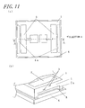
- the wiring board 10 of the second embodiment of the invention differs from the wiring board 10 of the preceding first embodiment in that, as exemplified in Figs. 9 to 11 , the insulating substrate 1 has a recess portion 1b provided in its side surface, and the wiring conductor 2 is partly exposed above the recess portion 1b from the side surface 1c of the insulating substrate 1 to provide an exposed portion 3.
- the wiring board 10 of this embodiment includes the wiring conductor 2 having the exposed portion 3 which is a part of the wiring conductor 2 which is exposed above the recess portion 1b from the side surface 1c of the insulating substrate 1, wherefore the distance from the exposed portion 3 on the side surface 1c of the insulating substrate 1 to the lower surface of the insulating substrate 1 can be increased, and correspondingly the distance between the exposed portion 3 of the wiring conductor 2 and the metal member 4 can be increased without causing an increase in the thickness of the wiring board 10.
- This makes it possible to suppress occurrence of ion migration between the exposed portion 3 of the wiring conductor 2 and the metal member 4, and thereby suppress electrical connection between the exposed portion 3 of the wiring conductor 2 and the metal member 4.
- the wiring board 10 can be made smaller in size when seen in a plan view.
- the concave length of the recess portion 1b is greater than or equal to 1.0 mm for the sake of suppressing occurrence of short-circuiting between the exposed portion 3 and the metal member 4 due to ion migration which arises between the exposed portion 3 and the metal member 4.
- the bonding material 5 is restrained from running up to the entire outer periphery of the insulating substrate 1, which is effective against the spread of the bonding material 5.
- the segmentable wiring board exemplified in Fig. 12 includes a 3 by 3 matrix of wiring board regions 11a, or a total of 9 wiring board regions 11a, each of which will constitute the insulating substrate 1 having the recess portion 1b-bearing side surface 1c.
- a forming region 11c for forming the recess portion 1b is provided in the outer edge of each of the wiring board regions 11a.
- the forming region 11c is intended to form the recess portion 1b in the insulating substrate 1 at the time of dividing the base board 11 into the wiring boards 10.
- the base board 11 With the provision of a void 12 in the forming region 11c of the base board 11, the base board 11 is divided into board segments along the outer edges of the individual wiring board regions 11a, thereby forming the recess portion 1b.
- the void 12 may be opened in the lower surface of the base board 11.
- the void 12 is opened, in contrast to a case where the void 12 is made as an enclosed space within the base board 11, during the firing of the green molded product of the base board 11, deformation of the recess portion 1b resulting from expansion of gas in the void 12 can be suppressed.
- the wiring board 10 may be constructed by bonding a plurality of insulating substrates 1 to a single metal member 4.
- both of the protrusion portion 1a and the recess portion 1b may be provided.
- the protrusion portion 1a will not be made thinner in part, wherefore the protrusion portion 1a can be protected from breakage during the manufacturing process.
- the exposed portion 3 may also be situated on the adjacent side surfaces 1c of the insulating substrate 1.
- the common conductors may be arranged in a grid pattern in the dummy regions 11b among the wiring board regions 11a.
- the thickness of the bonding material 5 from part to part so that the part corresponding to the midportion of the insulating substrate 1 is smaller in thickness than the part corresponding to the outer periphery of the insulating substrate 1, it is possible to afford the advantage to enhance the capability of heat dissipation from the insulating substrate 1 toward the metal member 4 in the middle of the insulating substrate 1 where the device is mounted.
Landscapes
- Engineering & Computer Science (AREA)
- Microelectronics & Electronic Packaging (AREA)
- Structure Of Printed Boards (AREA)
- Cooling Or The Like Of Semiconductors Or Solid State Devices (AREA)
Abstract
Description
- The present invention relates to a wiring board for installation of a device such as a light-emitting device, a semiconductor device, or a crystal oscillation device, an electronic apparatus constructed by mounting a device on the wiring board, and a segmentable wiring board.
- A conventionally-designed wiring board for installation of a device such as a light-emitting device or a semiconductor device is composed of, for example, an insulating substrate, a wiring conductor, and a metal member. For example, the wiring conductor is embedded in the insulating substrate so as to be partly exposed from a side surface of the insulating substrate. The metal member is bonded to the lower surface of the insulating substrate by a bonding member (refer to
Patent Literature 1, for example). - For example, a part of the wiring conductor which is partially exposed from the side surface of the insulating substrate results from the cutting-off of a plating wiring embedded in the base board of a segmentable wiring board entailed by the splitting of the segmentable wiring board.
- An electronic apparatus is constructed by mounting a device on such a wiring board and then electrically connecting the individual electrodes of the device to their respective wiring conductors via electrically connecting means such as solder or a bonding wire.
- Patent Literature 1: Japanese Unexamined Patent Publication
JP-A 2004-311791 - In recent years, as wiring boards have come to be lower in profile, the spacing between a metal member bonded to the lower surface of a wiring board and a wiring conductor exposed from a side surface of the wiring board is decreased correspondingly, which has given rise to a concern that the wiring conductor and the metal member may be electrically connected to each other due to ion migration arising between the wiring conductor exposed from the side surface of the wiring board and the metal member. In the event of an electrical connection being established between the wiring conductor exposed from the side surface of the wiring board and the metal member, short-circuiting will be caused in a plurality of wiring conductors via the metal member.
- The invention has been devised in view of the problems associated with the conventional art as mentioned above, and accordingly an object of the invention is to provide a wiring board capable of suppressing electrical connection between a wiring conductor exposed from a side surface of the wiring board and a metal member.
- According to one aspect of the invention, a wiring board includes an insulating substrate and a wiring conductor embedded in the insulating substrate and partly exposed from a side surface of the insulating substrate, and the side surface of the insulating substrate has a protrusion portion or recess portion located between the wiring conductor exposed from the side surface of the insulating substrate and a lower surface of the insulating substrate.
- According to another aspect of the invention, an electronic apparatus includes the wiring board constructed as described above and a device mounted on the wiring board.
- According to still another aspect of the invention, a segmentable wiring board includes a base board having a plurality of wiring board regions and a wiring conductor embedded in the base board so as to straddle the plural wiring board regions, and the base board also has a void provided between the wiring conductor of the base board and the lower surface of the base board so as to straddle a boundary of the plurality of wiring board regions.
- According to the wiring board pursuant to the invention, since the side surface has the protrusion portion or recess portion located between the wiring conductor exposed from the side surface and the lower surface of the insulating substrate, it is possible to suppress electrical connection between a part of the wiring conductor which is exposed from the side surface of the insulating substrate and a metal member bonded to the lower surface of the insulating substrate due to ion migration without causing an increase in the thickness of the wiring board.
-
-
Fig. 1(a) is a plan view showing a wiring board in accordance with a first embodiment of the invention, andFig. 1(b) is an example of a diagrammatic perspective view of part of the wiring board as viewed in a direction C indicated inFig. 1(a) ; -
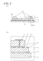
Fig. 2(a) is a sectional view taken along the line A-A shown inFig. 1(a) , andFig. 2(b) is an enlarged sectional view of a part A shown inFig. 2(a) ; -
Fig. 3(a) is a plan view showing the wiring board in accordance with the first embodiment of the invention, andFig. 3(b) is an example of a side view of the wiring board as viewed in a direction C indicated inFig. 3(a) ; -
Figs. 4(a) and 4(b) are each an example of a diagrammatic perspective view showing the wiring board in accordance with the first embodiment of the invention; -
Fig. 5(a) is a plan view showing the wiring board in accordance with the first embodiment of the invention, andFig. 5(b) is an example of a diagrammatic perspective view of part of the wiring board as viewed in a direction C indicated inFig. 5(a) ; -
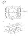
Fig. 6(a) is a sectional view taken along the line A-A shown inFig. 5(a) , andFig. 6(b) is a sectional view taken along the line B-B shown inFig. 3(a) ; -
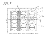
Fig. 7 is a plan view showing a segmentable wiring board in accordance with the first embodiment of the invention; -
Fig. 8(a) is a sectional view taken along the line A-A shown inFig. 7(a), andFig. 8(b) is an enlarged sectional view of a part A shown inFig. 8(a) ; -
Fig. 9(a) is a plan view showing the wiring board in accordance with the second embodiment of the invention, andFig. 9(b) is an example of a side view of the wiring board as viewed in a direction C indicated inFig. 9(a) ; -
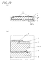
Fig. 10(a) is a sectional view taken along the line A-A shown inFig. 9(a) , andFig. 10(b) is an enlarged sectional view of a part A shown inFig. 10(a) ; -
Fig. 11(a) is a plan view showing the wiring board in accordance with a second embodiment of the invention, andFig. 11(b) is an example of a side view of the wiring board as viewed in a direction C indicated inFig. 11(a) ; -
Fig. 12(a) is a sectional view showing the segmentable wiring board in accordance with the second embodiment of the invention, andFig. 12(b) is an enlarged sectional view of a part A shown inFig. 12(a) ; and -
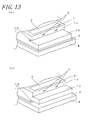
Figs. 13(a) and 13(b) are each an example of a perspective view showing the wiring board in accordance with an embodiment of the invention. - Hereinafter, several exemplificative embodiments of the invention will be described with reference to the accompanying drawings.
- As shown in
Figs. 1 and2 , an electronic apparatus in accordance with a first embodiment of the invention includes a wiring board 10 and a device 20 mounted on the wiring board 10. InFigs. 1 and2 , the electronic apparatus lies inside an imaginary space XYZ. InFigs. 1 and2 , an upward direction corresponds to a positive X-axis direction. - The wiring board 10 includes an
insulating substrate 1, awiring conductor 2 embedded in theinsulating substrate 1, and ametal member 4 bonded to the lower surface of theinsulating substrate 1. - The
insulating substrate 1 has a protrusion portion 1a provided in a side surface 1c thereof. The protrusion portion 1a is formed by jutting a lower part of the side surface 1c from theinsulating substrate 1 so that the protrusion portion 1a protrudes beyond the side surface 1c. It is preferable that the jutting length of the protrusion portion 1a is greater than or equal to 1.0 mm. For example, as exemplified inFig. 1 , the protrusion portion 1a is provided so as to extend along the entire width of the lower part of the side surface 1c when seen in a plan view. As employed herein, the expression "seen in a plan view" refers to the viewing of the construction in a direction C as indicated inFig. 1 . - In a case where the side surface of the protrusion portion 1a is greater in surface roughness than the upper surface of the protrusion portion 1a, the side surface of the protrusion portion 1a is more susceptible to moisture adhesion than is the upper surface of the protrusion portion 1a, wherefore moisture tends to collect on the side surface of the protrusion portion 1a and is thus less likely to adhere to the entire area of the protrusion portion 1a. As exemplified in
Fig. 3 by way of a modified form of the exemplification shown inFigs. 1 and2 , the protrusion portion 1a may be provided in only part of the lower part of the side surface 1c in the direction of its width when viewed in the direction C. In a case where the lower surface of theinsulating substrate 1 is flush with the lower surface of the protrusion portion 1a, in contrast to a case where the protrusion portion 1a is not provided, it is possible to increase the area of the lower surface of theinsulating substrate 1. - For example, in the case of placing a cap-like lid body on the upper surface of the wiring board 10, the upper surface of the protrusion portion 1a can be utilized for the bonding of the lid body. For example, a lid body having a lens or the like can be firmly bonded around the
insulating substrate 1 so as to hold theinsulating substrate 1. - As exemplified in
Figs. 1 and2 , theinsulating substrate 1 may include acavity 6. For example, thecavity 6 is provided in the upper surface of theinsulating substrate 1. - As the material for forming the
insulating substrate 1, ceramics or resin can be used. - For the
insulting substrate 1, in the case of using a ceramic material, for example, aluminum oxide sintered body (alumina ceramics), aluminum nitride sintered body, mullite sintered body or glass ceramic sintered body, can be used. On the other hand, for theinsulating substrate 1, in the case of using a resin material, for example, epoxy resin, polyimide resin, acrylic resin, phenol resin, polyester resin or fluorine-series resin such as tetrafluoroethylene resin, can be used. - In a modified form of the exemplification shown in
Figs. 1 and2 , as exemplified inFig. 4 , a concavity may be provided in the upper surface or the side surface of the protrusion portion 1a. The provision of the concavity makes it possible to shorten the jutting length of the protrusion portion 1a and thereby achieve downsizing of the wiring board 10. In the case of providing the protrusion portion 1a so as to extend over the entire lower part of the side surface 1c of theinsulating substrate 1, it is advisable to design the concavity as a slot extending along the entire protrusion portion 1a. Moreover, the concavity can be utilized for the bonding or retention of a lid body or a tab of the lid body. Otherwise, this modification example is structurally identical to the exemplification shown inFigs. 1 and2 . - In a modified form of the exemplification shown in
Figs. 1 and2 , in a case where thecavity 6 is intended for the installation of a light-emitting device, as exemplified inFigs. 5 and6 , it is preferable that an angle θ formed between the inner side surface of thecavity 6 and the bottom surface of thecavity 6 is an obtuse angle, in particular an obtuse angle of 110° to 145°. By adjusting the angle θ to fall in the above-described range, the inner side surface of the through hole constituting thecavity 6 can be created in an efficient manner with stability by means of punching, and thus a light-emitting apparatus which employs this wiring board 10 can be downsized readily. Moreover, light emitted from the light-emitting device is allowed to radiate outward satisfactorily. - The
wiring conductor 2 is embedded in theinsulating substrate 1 and is partly exposed above the protrusion portion 1a from the side surface 1c of theinsulating substrate 1 . A part of thewiring conductor 2 which is exposed from the side surface 1c of theinsulating substrate 1 will be defined as an exposedportion 3. Moreover, an end of thewiring conductor 2 is led out to the top side. - For example, the exposed
portion 3 is utilized for the passage of an electric current used to deposit a plating layer on the surface of the part of thewiring conductor 2 leading onto the upper surface of the insulatingsubstrate 1 by electrolytic plating technique. Moreover, for example, where a terminal electrode for making connection with an external circuit board is disposed on the side surface 1c of the insulatingsubstrate 1, the exposedportion 3 may be electrically connected to the terminal electrode. - For example, in the exemplifications shown in
Figs. 1 to 6 , the parts of thewiring conductor 2 leading onto the top side are arranged on the upper surface of the insulatingsubstrate 1 so as to sandwich thecavity 6 between them. Thewiring conductor 2 is electrically connected to the device mounted on the upper surface of the insulatingsubstrate 1 and the wiring of an external circuit board as well. - As exemplified in
Fig. 5 , thewiring conductor 2 may be so designed that an end thereof is led out to a plurality of locations on the top side. Parts of thewiring conductor 2 led out to the plurality of locations on the top side are electrically connected to their respective wirings of the external circuit board. - The
wiring conductor 2 has the exposedportion 3 which is a part of an end thereof which is exposed from the side surface 1c of the insulatingsubstrate 1. - Moreover, where a plurality of exposed
portions 3 are provided in one and the same side surface 1c of the insulatingsubstrate 1, it is desirable to adjust the spacing between the exposedportions 3 to be greater than or equal to 1.0 mm to suppress ion migration between the exposedportions 3. - In the case of providing the plurality of exposed
portions 3 in one side surface 1c, as exemplified inFig. 5 , by spacing the plurality of exposedportions 3 apart also in a thickness direction of the insulatingsubstrate 1, it is possible to increase the spacing between the exposedportions 3. In order for the exposedportions 3 to be spaced apart in the thickness direction of the insulatingsubstrate 1, for example, when the insulatingsubstrate 1 is composed of a plurality of insulating layers, it is advisable to interpose thewiring conductor 2 between the discrete insulating layers. - For such a
wiring conductor 2, a metal material such as tungsten (W), molybdenum (Mo), manganese (Mn), silver (Ag), or copper (Cu) can be used. For example, where the insulatingsubstrate 1 is made of aluminum oxide sintered body, thewiring conductor 2 can be deposited in a predetermined location of the insulatingsubstrate 1 by print-coating a conductor paste, which has been prepared by admixing suitable organic binder and solvent in powder of a high-melting-point metal such as W, Mo, Mn, or the like, in a predetermined pattern on a ceramic green sheet for forming the insulatingsubstrate 1 by means of screen printing, and then co-firing the paste together with the ceramic green sheet for forming the insulatingsubstrate 1. In a case where thewiring conductor 2 is designed as a through conductor, a through hole is created by punching a hole in the green sheet with a die or by subjecting the sheet to lasering prior to the formation of the conductor pattern for forming thewiring conductor 2 formed on the top side, and the conductor paste is charged into the through hole by means of printing, whereby the through conductor can be formed. - The exposed surface of the
wiring conductor 2 is plated with a plating layer by the electrolytic plating technique. The plating layer is made of a metal which excels in corrosion resistance and in bondability with a connecting member, such as nickel, copper, gold, or silver. For example, a copper plating layer having a thickness in a range of 0.5 µm to 5 µm approximately, a nickel plating layer having a thickness in a range of 0.5 µm to 5 µm approximately, and a gold plating layer having a thickness in a range of 0.1 µm to 3 µm approximately, or, a nickel plating layer having a thickness in a range of 1 µm to 10 µm approximately, and a silver plating layer having a thickness in a range of 0.1 µm to 1 µm approximately, are deposited one after another on the surface. This makes it possible to protect thewiring conductor 2 from corrosion effectively, as well as to strengthen the adhesion between the device and thewiring conductor 2, the connection between thewiring conductor 2 and the connecting member such as a bonding wire, the connection between an external terminal and a wiring conductor of an external circuit board, and the connection between themetal member 4 and a conductor of the external circuit board. - The
metal member 4 is bonded to the lower surface of the insulatingsubstrate 1. Themetal member 4 can be prepared with use of a material which is higher in heat conductivity than the insulatingsubstrate 1, for example, a metal material such as copper (Cu), copper-tungsten (Cu-W), or aluminum (Al). For example, where the insulatingsubstrate 1 is made of aluminum oxide sintered body, a material which is higher in heat conductivity than the insulatingsubstrate 1, such as Cu, can be used as the material of formation of themetal member 4. With the provision of themetal member 4 having high heat conductivity, the wiring board 10 is capable of dissipating heat generated by the device mounted thereon in an efficient manner, which leads to improvement in heat dissipation capability. - The
metal member 4 is brazed to the lower surface of the insulatingsubstrate 1 with use of abonding material 5 such for example as a brazing material made of a silver-copper alloy. It is preferable that, in the wiring board 10, a metal is attached to the lower surface of the insulatingsubstrate 1 for the placement of thebonding material 5. In a case where an active brazing metal with added active metal such as Ti, or a resin material in admixture with a metal material having high heat conductivity is used as thebonding material 5, themetal member 4 is bonded to the insulatingsubstrate 1 through thebonding material 5 attached directly to the insulatingsubstrate 1. - In a case where the wiring board 10 includes the insulating
substrate 1 whose upper surface bears thecavity 6 for the installation of a light-emitting device for example, as exemplified inFigs. 5 and6 , it is advisable to provide a reflection layer in the inner wall surface of thecavity 6 for the reflection of light emitted from the light-emitting device. - For example, the reflection layer includes a
metal layer 7 attached to the inner wall surface of thecavity 6 and a plating layer deposited on themetal layer 7. Moreover, themetal layer 7 may be electrically connected to thewiring conductor 2. - The
metal layer 7 is formed flatly on the inner wall surface of thecavity 6 by the use of the same material and method as those used in the formation of thewiring conductor 2. As the conductor paste for themetal layer 7, the same as the conductor paste for thewiring conductor 2 can be used, or, in the interest of printing capability, it is also possible to use a conductor paste which differs from that conductor paste in respect of the type or amount of the constituent organic binder or solvent. - The plating layer deposited on the surface of the
metal layer 7 can be formed of the same material as that constituting the plating layer deposited on the exposed surface of thewiring conductor 2. - For example, in the case of mounting a light-emitting device on the wiring board 10, it is preferable that a silver plating layer is deposited on the surface of the
metal layer 7, and a gold plating layer is deposited on the surface of thewiring conductor 2. This is because the gold plating layer is superior to the silver plating layer in point of bondability to the connecting member and the wiring conductor of the external circuit board, while the silver plating layer is higher in light reflectivity than the gold plating layer. Alternatively, the outermost layer of each of thewiring conductor 2 and themetal layer 7 may be provided as a silver-gold alloy plating layer, for example, an alloy plating layer made of a complete solid solution of silver and gold. - In a case where the plating layer deposited on the surface of the
metal layer 7 is deposited by the electrolytic plating technique, it is advisable that thewiring conductor 2 connected to themetal layer 7 is provided additionally on the insulatingsubstrate 1. In a case where the plating layer deposited on the surface of thewiring conductor 2 and the plating layer deposited on the surface of themetal layer 7 are made of the same material, it is advisable that themetal layer 7 and thewiring conductor 2 are electrically connected to each other. - The
metal layer 7 may disposed on the entire surface of the bottom and inner side of thecavity 6, and also thewiring conductor 2 may be disposed around thecavity 6 on the upper surface of the insulatingsubstrate 1. - Moreover, one of a pair of
wiring conductors 2 each having its one end led out to the upper surface of the insulatingsubstrate 1 may be bonded to themetal layer 7 disposed on the bottom surface of thecavity 6 as well as on the inner side surface of thecavity 6. This is effective at rendering the wiring board 10 lower in profile, because there is no need to bury thewiring conductor 2 made for themetal layer 7 in the insulatingsubstrate 1. - In the wiring board 10 for the installation of a light-emitting device for example, where a reflection layer for reflecting light emitted from the light-emitting device is formed on the entire inner surface of the
cavity 6, so long as the light-emitting face of the light-emitting device is situated inside thecavity 6, it is possible to increase the luminance of a light-emitting apparatus employing the wiring board. - The electronic apparatus can be constructed by mounting a device on the upper surface of the wiring board 10.
- Examples of the device mounted on the wiring board 10 include a semiconductor device such as an IC chip and an LSI chip, a light-emitting device, a piezoelectric element such as a crystal oscillator and a piezoelectric oscillator, and sensors of various types.
- For example, where the device is a semiconductor device of flip-chip mounting type, the semiconductor device is mounted on the wiring board 10 by establishing electrical and mechanical connection between the electrode of the semiconductor device and the
wiring conductor 2 via a bonding member such as a solder bump, a gold bump, or an electrically conductive resin (such as an anisotropic conductive resin). - On the other hand, for example, where the device is a semiconductor device of wire bonding type, the semiconductor device is, after being secured to a device mounting region by a bonding member, mounted on the wiring board 10 by establishing an electrical connection between the electrode of the semiconductor device and the
wiring conductor 2 via a bonding wire. - Moreover, the wiring board 10 of the first embodiment can be produced in an efficient manner by splitting a segmentable wiring board 10 as exemplified in
Figs. 7 and8 . - The segmentable wiring board exemplified in
Figs. 7 and8 includes a 3 by 3 matrix of wiring board regions 11a, or a total of 9 wiring board regions 11a, each of which will constitute the insulatingsubstrate 1 having the protrusion portion 1a-bearing side surface 1c. - It is sufficient that a plurality of wiring board regions 11a are aligned in at least one of the lengthwise direction and the widthwise direction. While the exemplification shown in
Figs. 7 and8 has the 3 by 3 wiring board region 11a matrix, the number of the wiring board regions 11a to be arranged can be increased. The wiring board region 11a is designed with consideration given to the sizes of abase board 11 and the wiring board region 11a, the placement of the device and thewiring conductor 2 on the wiring board region 11a, and so forth. - The
base board 11 has, in the exemplification shown inFigs. 7 and8 for example, a dummy region 11b formed around the matrix of the plurality of wiring board regions 11a (the outer periphery of the base board 11). The dummy region 11b is intended to facilitate the production and transportation of the segmentable wiring board, and, by the use of this dummy region 11b, it is possible to effect the positioning, fastening, etc. of a green molded product prepared for thebase board 11 or the segmentable wiring board for machining operation and transportation. - The dummy region 11b may be provided with a common conductor which is electrically connected to the
wiring conductor 2. It is preferable that the plurality ofwiring conductors 2 are electrically connected to each other by the common conductor disposed in the dummy region 11b, because, in this case, an electric current for electrolytic plating can be passed from at least one point of the common conductor. - The provision of the common conductor in frame form in the dummy region 11b affords the advantage to lessen thickness variations among the plating layers deposited on the
wiring conductors 2 of the wiring board regions 11a, respectively. By adjusting the cross-sectional area of the common conductor to be greater than the cross-sectional area of thewiring conductor 2, it is possible to suppress resistance increase in the common conductor. - A forming
region 11c for forming the protrusion portion 1a is provided in the outer edge of each of the wiring board regions 11a. The formingregion 11c is intended to form the protrusion portion 1a in the insulatingsubstrate 1 at the time of dividing thebase board 11 into the wiring boards 10. With the provision of a void 12 in the formingregion 11c of thebase board 11, thebase board 11 is divided into board segments along the outer edges of the individual wiring board regions 11a, thereby forming the protrusion portions 1a. For example, such avoid 12 is created by causing the insulating layers to separate from each other in the shoulder-formingregion 11c under the condition where, at the time of stacking a plurality of ceramic green sheets on top of each other in layers under pressure, no pressure is applied to the shoulder-formingregion 11c, or the shoulder-formingregion 11c is subjected to a pressure lower than in other regions. - The void 12 can be created also by stacking together a plurality of ceramic green sheets having holes constituting the void 12 formed therethrough by means of lasering, die punching, or otherwise and through hole-free ceramic green sheets, and then firing the resultant laminated body. Moreover, where the
base board 11 has a small thickness, it is possible to create through holes constituting the void 12 by means of lasering, die punching, or otherwise after the stacking of a plurality of ceramic green sheets. - In the segmentable wiring board for the production of the wiring board 10 having the side surface 1c bearing the protrusion portion 1a, as exemplified in
Fig. 8 , it is advisable that the void 12 is made wider than the outer edge of the wiring board region 11a on the top side. This makes it possible to reduce a possibility that a line of demarcation and the void 12 will not overlap each other as seen transparently in a plan view. Moreover, in the process of splitting the board by means of slicing or otherwise, by making a cut to a depth in which the void 12 is formed, it possible to reduce a possibility that the protrusion portion 1a will be cut off. - The void 12 may be opened in the upper surface or lower surface of the
base board 11. In the case where the void 12 is opened, in contrast to a case where the void 12 is made as an enclosed space within thebase board 11, during the firing of the green molded product of thebase board 11, deformation of the protrusion portion 1a resulting from expansion of gas in the void 12 can be suppressed. - In the range of the outer edge of the wiring board region 11a, by forming a division groove, which is so shaped that its cross section becomes wider gradually in the direction toward its opening, in the upper surface or lower surface of the
base board 11, it is easy to split the board along the outer edges of the individual wiring board regions 11a successfully. - By splitting the segmentable wiring board along the outer edges of the individual wiring board regions 11a, the insulating
substrates 1 as exemplified inFigs. 1 to 6 can be formed. Then, themetal member 4 is bonded to the lower surface of the insulatingsubstrate 1, thereby producing the wiring board 10. Moreover, the division of the segmentable wiring board allows production of the wiring board 10 having the exposedportion 3 which is a part of thewiring conductor 2 which is exposed from the side surface 1c of the insulatingsubstrate 1. - The division of the board along the outer edges of the wiring board regions 11a may be carried out after the bonding of the
metal member 4 to the lower surface of each of the wiring board regions 11a. Note that, as exemplified inFigs. 1 to 6 , in the case of producing the wiring board 10 with the bondedmetal member 4 which is larger in width than the insulatingsubstrate 1, it is advisable to form the dummy region 11b around each of the wiring board regions 11a in the segmentable wiring board. - It is also possible to split the segmentable wiring board after the installation of the device on the upper surface of each of the wiring board regions 11a.
- The
base board 11 can be divided into a plurality of insulatingsubstrates 1 by, for example, a method including forming a division groove in the outer edge of the wiring board region 11a of thebase board 11 and bending the base board along the division groove until it is split, or a method including cutting the base board along the outer edge of the wiring board region 11a by means of slicing or otherwise. The division groove can be obtained by making an incision in a green molded product prepared for thebase board 11 by sticking a cutter blade into the green molded product or by using slicing equipment in such a manner that the dimension of the incision is smaller than the thickness of the green molded product, or by making an incision after a firing process by slicing equipment in such a manner that its dimension is smaller than the thickness of thebase board 11. - In the case of splitting the board through a cutting process by means of slicing or otherwise, so long as two slicing blades of different widths are applied to the upper surface and the lower surface, respectively, of the
base board 11, the protrusion portion 1a may be created by effecting cutting operation using slicing equipment without the necessity of forming the void 12 described above. - In the wiring board 10 of this embodiment, the side surface 1c is formed with the protrusion portion 1a located between the
wiring conductor 2 exposed from the side surface 1c and the lower surface of the insulatingsubstrate 1, wherefore the distance from the exposedportion 3 on the side surface 1c of the insulatingsubstrate 1 to the lower surface of the insulatingsubstrate 1 can be increased, and correspondingly the distance between the exposedportion 3 of thewiring conductor 2 and themetal member 4 can be increased without causing an increase in the thickness of the wiring board 10. This makes it possible to suppress occurrence of ion migration between the exposedportion 3 of thewiring conductor 2 and themetal member 4, and thereby suppress electrical connection between the exposedportion 3 of thewiring conductor 2 and themetal member 4. - In a case where the protrusion portion 1a has a region which is greater in surface roughness than the side surface 1c, the side surface of the protrusion portion 1a is more susceptible to moisture adhesion than is the upper surface of the protrusion portion 1a, wherefore moisture tends to collect on the side surface of the protrusion portion 1a and is thus less likely to adhere to the entire area ranging from the exposed
portion 3 to themetal member 4, which is effective against ion migration. - Moreover, the provision of the protrusion portion 1a in the insulating
substrate 1 makes it possible to restrain thebonding material 5 from running up toward the side surface 1c, and thereby suppress that thebonding material 5 will spread over the side surface 1c and eventually reach the exposedportion 3. - The segmentable wiring board of this embodiment includes the
base board 11 having a plurality of wiring board regions 11a and thewiring conductor 2 embedded in thebase board 11 so as to straddle the plurality of wiring board regions 11a, and thebase board 11 has the void 12 provided between thewiring conductor 2 of thebase board 11 and the lower surface of thebase board 1 so as to straddle the boundary of the plurality of wiring board regions 11a. By splitting such a segmentable wiring board, the insulatingsubstrate 1 of the wiring board 10 of this embodiment can be produced in an efficient manner. - Moreover, where the segmentable wiring board of this embodiment further includes the
metal member 4 bonded to the lower surfaces of the wiring board regions 11a of thebase board 11, the wiring board 10 of this embodiment can be produced in an efficient manner. - Next, an electronic apparatus in accordance with the second embodiment of the invention will be described with reference to
Figs. 9 to 11 . - The wiring board 10 of the second embodiment of the invention differs from the wiring board 10 of the preceding first embodiment in that, as exemplified in
Figs. 9 to 11 , the insulatingsubstrate 1 has a recess portion 1b provided in its side surface, and thewiring conductor 2 is partly exposed above the recess portion 1b from the side surface 1c of the insulatingsubstrate 1 to provide an exposedportion 3. - The wiring board 10 of this embodiment includes the
wiring conductor 2 having the exposedportion 3 which is a part of thewiring conductor 2 which is exposed above the recess portion 1b from the side surface 1c of the insulatingsubstrate 1, wherefore the distance from the exposedportion 3 on the side surface 1c of the insulatingsubstrate 1 to the lower surface of the insulatingsubstrate 1 can be increased, and correspondingly the distance between the exposedportion 3 of thewiring conductor 2 and themetal member 4 can be increased without causing an increase in the thickness of the wiring board 10. This makes it possible to suppress occurrence of ion migration between the exposedportion 3 of thewiring conductor 2 and themetal member 4, and thereby suppress electrical connection between the exposedportion 3 of thewiring conductor 2 and themetal member 4. - In this way, where the insulating
substrate 1 has the recess portion 1b situated toward its lower surface beyond the exposedportion 3, in contrast to the case of providing the protrusion portion 1a, the wiring board 10 can be made smaller in size when seen in a plan view. - It is preferable that the concave length of the recess portion 1b is greater than or equal to 1.0 mm for the sake of suppressing occurrence of short-circuiting between the exposed
portion 3 and themetal member 4 due to ion migration which arises between the exposedportion 3 and themetal member 4. - As exemplified in
Fig. 9 , by providing the recess portion 1b so as to extend entirely longitudinally of the side surface 1c provided with the exposedportion 3 in a plan view seen from the direction C, it is possible to suppress ion migration over the entire side surface 1c provided with the exposedportion 3. - As exemplified in
Fig. 9 , by providing the recess portion 1b in each and every side surface 1c of the rectangular insulatingsubstrate 1, thebonding material 5 is restrained from running up to the entire outer periphery of the insulatingsubstrate 1, which is effective against the spread of thebonding material 5. - As exemplified in
Fig. 10 , by providing the recess portion 1b in part of the side surface 1c of the insulatingsubstrate 1, it is possible to suppress a decrease in the area of adhesion between the insulatingsubstrate 1 and themetal member 4, and thereby suppress deterioration in the capability of heat dissipation in the insulatingsubstrate 1 and themetal member 4. - The segmentable wiring board exemplified in
Fig. 12 includes a 3 by 3 matrix of wiring board regions 11a, or a total of 9 wiring board regions 11a, each of which will constitute the insulatingsubstrate 1 having the recess portion 1b-bearing side surface 1c. - A forming
region 11c for forming the recess portion 1b is provided in the outer edge of each of the wiring board regions 11a. The formingregion 11c is intended to form the recess portion 1b in the insulatingsubstrate 1 at the time of dividing thebase board 11 into the wiring boards 10. With the provision of a void 12 in the formingregion 11c of thebase board 11, thebase board 11 is divided into board segments along the outer edges of the individual wiring board regions 11a, thereby forming the recess portion 1b. - As exemplified in
Fig. 12 , the void 12 may be opened in the lower surface of thebase board 11. In the case where the void 12 is opened, in contrast to a case where the void 12 is made as an enclosed space within thebase board 11, during the firing of the green molded product of thebase board 11, deformation of the recess portion 1b resulting from expansion of gas in the void 12 can be suppressed. - It should be noted that the invention is not limited to the exemplificative embodiments as described heretofore, and therefore various changes and modifications are possible. For example, the wiring board 10 may be constructed by bonding a plurality of insulating
substrates 1 to asingle metal member 4. - As exemplified in
Figs. 13(a) and 13(b) , both of the protrusion portion 1a and the recess portion 1b may be provided. - Moreover, as exemplified in
Fig. 13(a) , where the recess portion is provided above the protrusion portion 1a in the side surface 1c, in contrast to the case of providing the recess portion in the upper surface of the protrusion portion 1a, the protrusion portion 1a will not be made thinner in part, wherefore the protrusion portion 1a can be protected from breakage during the manufacturing process. - Further, the exposed
portion 3 may also be situated on the adjacent side surfaces 1c of the insulatingsubstrate 1. - In the
base board 11, where the dummy region 11b is formed around each of the wiring board regions 11a, the common conductors may be arranged in a grid pattern in the dummy regions 11b among the wiring board regions 11a. - By varying the thickness of the
bonding material 5 from part to part so that the part corresponding to the midportion of the insulatingsubstrate 1 is smaller in thickness than the part corresponding to the outer periphery of the insulatingsubstrate 1, it is possible to afford the advantage to enhance the capability of heat dissipation from the insulatingsubstrate 1 toward themetal member 4 in the middle of the insulatingsubstrate 1 where the device is mounted. -
- 1: Insulating substrate
- 1a: Protrusion portion
- 1b: Concavity portion
- 1c: Side surface
- 2: Wiring conductor
- 3: Exposed portion
- 4: Metal member
- 5: Bonding material
- 6: Cavity
- 7: Metal layer
- 10: Wiring board
- 11: Base board
- 11a: Wiring board region
- 11b: Dummy region
- 11c: Forming region
- 12: Void
Claims (6)
- A wiring board, comprising:an insulating substrate; anda wiring conductor embedded in the insulating substrate and partly exposed from a side surface of the insulating substrate,the side surface of the insulating substrate having a protrusion portion or a recess portion located between the wiring conductor exposed from the side surface of the insulating substrate and a lower surface of the insulating substrate.
- The wiring board according to claim 1, further comprising:a metal member bonded to the lower surface of the insulating substrate.
- The wiring board according to claim 1 or 2,
wherein the recess portion or the protrusion portion has a region which is greater in surface roughness than the side surface of the insulating substrate. - An electronic apparatus, comprising:the wiring board according to claim 2 or 3; andan electronic device mounted on the wiring board.
- A segmentable wiring board, comprising:a base board having a plurality of wiring board regions; anda wiring conductor embedded in the base board so as to straddle the plurality of wiring board regions,the base board has a void provided between the wiring conductor of the base board and a lower surface of the base board so as to straddle a boundary of the plurality of wiring board regions.
- The segmentable wiring board according to claim 5, further comprising:a metal member bonded to lower surfaces of the wiring board regions of the base board.
Applications Claiming Priority (2)
| Application Number | Priority Date | Filing Date | Title |
|---|---|---|---|
| JP2010240988 | 2010-10-27 | ||
| PCT/JP2011/074862 WO2012057286A1 (en) | 2010-10-27 | 2011-10-27 | Wiring board |
Publications (3)
| Publication Number | Publication Date |
|---|---|
| EP2634797A1 true EP2634797A1 (en) | 2013-09-04 |
| EP2634797A4 EP2634797A4 (en) | 2016-08-10 |
| EP2634797B1 EP2634797B1 (en) | 2019-05-08 |
Family
ID=45993989
Family Applications (1)
| Application Number | Title | Priority Date | Filing Date |
|---|---|---|---|
| EP11836419.9A Active EP2634797B1 (en) | 2010-10-27 | 2011-10-27 | Wiring board |
Country Status (5)
| Country | Link |
|---|---|
| US (1) | US9485867B2 (en) |
| EP (1) | EP2634797B1 (en) |
| JP (1) | JP5678085B2 (en) |
| CN (1) | CN103180941B (en) |
| WO (1) | WO2012057286A1 (en) |
Cited By (2)
| Publication number | Priority date | Publication date | Assignee | Title |
|---|---|---|---|---|
| EP2993395A1 (en) * | 2014-09-03 | 2016-03-09 | Toshiba Lighting & Technology Corporation | Lighting device for moving body |
| WO2019042653A1 (en) * | 2017-08-29 | 2019-03-07 | Conti Temic Microelectronic Gmbh | CIRCUIT BOARD FOR POWER ELECTRONICS AND POWER ELECTRONIC MODULE WITH A CIRCUIT CARRIER |
Families Citing this family (9)
| Publication number | Priority date | Publication date | Assignee | Title |
|---|---|---|---|---|
| JP5724573B2 (en) * | 2011-04-19 | 2015-05-27 | 日亜化学工業株式会社 | Light emitting device |
| US10165669B2 (en) | 2011-12-22 | 2018-12-25 | Kyocera Corporation | Wiring board and electronic device |
| WO2014128796A1 (en) | 2013-02-25 | 2014-08-28 | パナソニック株式会社 | Semiconductor device |
| EP2914071A1 (en) * | 2014-02-28 | 2015-09-02 | AT & S Austria Technologie & Systemtechnik Aktiengesellschaft | Heat spreader in multilayer build ups |
| JP6829303B2 (en) * | 2017-02-23 | 2021-02-10 | 京セラ株式会社 | Insulation substrates, semiconductor packages and semiconductor devices |
| JP2019083264A (en) * | 2017-10-30 | 2019-05-30 | 日本特殊陶業株式会社 | Wiring board and wiring board for multiple parts |
| CN214507497U (en) * | 2018-09-28 | 2021-10-26 | 株式会社村田制作所 | collective substrate |
| JP7443281B2 (en) * | 2021-03-22 | 2024-03-05 | 株式会社東芝 | wiring device |
| WO2026070842A1 (en) * | 2024-09-27 | 2026-04-02 | 京セラ株式会社 | Wiring board, electronic component storage package, and electronic module |
Family Cites Families (19)
| Publication number | Priority date | Publication date | Assignee | Title |
|---|---|---|---|---|
| JPS5816552A (en) | 1981-07-22 | 1983-01-31 | Fujitsu Ltd | Package for semiconductor element |
| US4694123A (en) * | 1982-01-13 | 1987-09-15 | Elxsi | Backplane power connector system |
| US4630172A (en) * | 1983-03-09 | 1986-12-16 | Printed Circuits International | Semiconductor chip carrier package with a heat sink |
| JPH088321B2 (en) * | 1987-01-19 | 1996-01-29 | 住友電気工業株式会社 | Integrated circuit package |
| US5136471A (en) * | 1987-02-26 | 1992-08-04 | Nec Corporation | Laminate wiring board |
| US5219292A (en) * | 1992-04-03 | 1993-06-15 | Motorola, Inc. | Printed circuit board interconnection |
| EP0582881B1 (en) * | 1992-07-27 | 1997-12-29 | Murata Manufacturing Co., Ltd. | Multilayer electronic component, method of manufacturing the same and method of measuring characteristics thereof |
| US5461070A (en) * | 1994-08-29 | 1995-10-24 | The Regents Of The University Of California | Anti-flammatory method using indole alkaloids |
| US7348494B1 (en) * | 2000-12-15 | 2008-03-25 | Nortel Networks Limited | Signal layer interconnects |
| CN102290409B (en) | 2003-04-01 | 2014-01-15 | 夏普株式会社 | Light-emitting apparatus |
| JP2004311791A (en) | 2003-04-08 | 2004-11-04 | Sharp Corp | Lighting device, backlight device and display device |
| JP4931334B2 (en) * | 2004-05-27 | 2012-05-16 | 京セラ株式会社 | Injection device |
| JP4698259B2 (en) | 2005-03-16 | 2011-06-08 | 三洋電機株式会社 | Electronic component mounting package and package assembly board |
| JP2007019394A (en) | 2005-07-11 | 2007-01-25 | Toshiba Corp | Semiconductor package manufacturing method and semiconductor package formed by the manufacturing method |
| JP2007311378A (en) * | 2006-05-16 | 2007-11-29 | Renesas Technology Corp | Semiconductor device manufacturing method and semiconductor device |
| JP2008130701A (en) | 2006-11-20 | 2008-06-05 | Matsushita Electric Ind Co Ltd | WIRING BOARD, SEMICONDUCTOR DEVICE USING SAME, AND METHOD FOR MANUFACTURING SEMICONDUCTOR DEVICE |
| EP2237316B1 (en) * | 2008-01-30 | 2019-10-09 | Kyocera Corporation | Connection terminal, package using the same and electronic device |
| JP2009290021A (en) * | 2008-05-29 | 2009-12-10 | Toshiba Corp | Part-incorporated printed wiring board, method for manufacturing the wiring board, and electronic apparatus |
| JP5235627B2 (en) * | 2008-08-21 | 2013-07-10 | 京セラ株式会社 | Multiple wiring board |
-
2011
- 2011-10-27 US US13/880,589 patent/US9485867B2/en active Active
- 2011-10-27 WO PCT/JP2011/074862 patent/WO2012057286A1/en not_active Ceased
- 2011-10-27 CN CN201180040339.9A patent/CN103180941B/en active Active
- 2011-10-27 EP EP11836419.9A patent/EP2634797B1/en active Active
- 2011-10-27 JP JP2012540943A patent/JP5678085B2/en active Active
Cited By (3)
| Publication number | Priority date | Publication date | Assignee | Title |
|---|---|---|---|---|
| EP2993395A1 (en) * | 2014-09-03 | 2016-03-09 | Toshiba Lighting & Technology Corporation | Lighting device for moving body |
| US9709250B2 (en) | 2014-09-03 | 2017-07-18 | Toshiba Lighting & Technology Corporation | Lighting device for moving body |
| WO2019042653A1 (en) * | 2017-08-29 | 2019-03-07 | Conti Temic Microelectronic Gmbh | CIRCUIT BOARD FOR POWER ELECTRONICS AND POWER ELECTRONIC MODULE WITH A CIRCUIT CARRIER |
Also Published As
| Publication number | Publication date |
|---|---|
| EP2634797B1 (en) | 2019-05-08 |
| CN103180941B (en) | 2016-06-29 |
| US20140000940A1 (en) | 2014-01-02 |
| US9485867B2 (en) | 2016-11-01 |
| WO2012057286A1 (en) | 2012-05-03 |
| JPWO2012057286A1 (en) | 2014-05-12 |
| CN103180941A (en) | 2013-06-26 |
| EP2634797A4 (en) | 2016-08-10 |
| JP5678085B2 (en) | 2015-02-25 |
Similar Documents
| Publication | Publication Date | Title |
|---|---|---|
| US9485867B2 (en) | Wiring board | |
| JP6483800B2 (en) | Light emitting element mounting package, light emitting device, and light emitting module | |
| EP3136430B1 (en) | Wiring board, electronic device, and electronic module | |
| EP3062590B1 (en) | Wiring board and electronic device | |
| CN104412722B (en) | Circuit board, electronic device and light-emitting device | |
| EP3846202A1 (en) | Wiring board, electronic device and electronic module | |
| EP3030060B1 (en) | Wiring base plate and electronic device | |
| JP5855822B2 (en) | Multiple wiring board | |
| JP4458974B2 (en) | Multiple wiring board | |
| JP6224473B2 (en) | Wiring board, electronic device and electronic module | |
| JP3842683B2 (en) | Multi-wiring board | |
| JP5574848B2 (en) | Multiple wiring board | |
| JP2007043061A (en) | Multiple wiring board | |
| JP2005340562A (en) | Multiple wiring board | |
| JP5679827B2 (en) | Wiring board and multi-cavity wiring board | |
| JP2006128297A (en) | Multi-circuit board and electronic device | |
| JP2004179543A (en) | Multi-cavity wiring board | |
| JP2005019751A (en) | Multi-wiring board | |
| JP2004356353A (en) | Multi-cavity wiring board | |
| JP2004288856A (en) | Multi-cavity wiring board | |
| JP2001210742A (en) | Electronic component mounting board and multi-cavity array board | |
| JP2007173630A (en) | Multiple wiring board | |
| JP2004288932A (en) | Multi-cavity wiring board | |
| JP2005191104A (en) | Multiple wiring board |
Legal Events
| Date | Code | Title | Description |
|---|---|---|---|
| PUAI | Public reference made under article 153(3) epc to a published international application that has entered the european phase |
Free format text: ORIGINAL CODE: 0009012 |
|
| 17P | Request for examination filed |
Effective date: 20130527 |
|
| AK | Designated contracting states |
Kind code of ref document: A1 Designated state(s): AL AT BE BG CH CY CZ DE DK EE ES FI FR GB GR HR HU IE IS IT LI LT LU LV MC MK MT NL NO PL PT RO RS SE SI SK SM TR |
|
| DAX | Request for extension of the european patent (deleted) | ||
| REG | Reference to a national code |
Ref country code: DE Ref legal event code: R079 Ref document number: 602011058861 Country of ref document: DE Free format text: PREVIOUS MAIN CLASS: H01L0023360000 Ipc: H01L0023000000 |
|
| RA4 | Supplementary search report drawn up and despatched (corrected) |
Effective date: 20160713 |
|
| RIC1 | Information provided on ipc code assigned before grant |
Ipc: H01L 33/48 20100101ALI20160707BHEP Ipc: H01L 23/00 20060101AFI20160707BHEP Ipc: H05K 1/02 20060101ALI20160707BHEP Ipc: H01L 23/12 20060101ALI20160707BHEP Ipc: H01L 23/36 20060101ALI20160707BHEP Ipc: H05K 3/00 20060101ALI20160707BHEP Ipc: H01L 23/13 20060101ALI20160707BHEP Ipc: H01L 33/62 20100101ALI20160707BHEP Ipc: H01L 23/498 20060101ALI20160707BHEP |
|
| STAA | Information on the status of an ep patent application or granted ep patent |
Free format text: STATUS: EXAMINATION IS IN PROGRESS |
|
| 17Q | First examination report despatched |
Effective date: 20170703 |
|
| GRAP | Despatch of communication of intention to grant a patent |
Free format text: ORIGINAL CODE: EPIDOSNIGR1 |
|
| STAA | Information on the status of an ep patent application or granted ep patent |
Free format text: STATUS: GRANT OF PATENT IS INTENDED |
|
| INTG | Intention to grant announced |
Effective date: 20190110 |
|
| GRAS | Grant fee paid |
Free format text: ORIGINAL CODE: EPIDOSNIGR3 |
|
| GRAA | (expected) grant |
Free format text: ORIGINAL CODE: 0009210 |
|
| STAA | Information on the status of an ep patent application or granted ep patent |
Free format text: STATUS: THE PATENT HAS BEEN GRANTED |
|
| AK | Designated contracting states |
Kind code of ref document: B1 Designated state(s): AL AT BE BG CH CY CZ DE DK EE ES FI FR GB GR HR HU IE IS IT LI LT LU LV MC MK MT NL NO PL PT RO RS SE SI SK SM TR |
|
| REG | Reference to a national code |
Ref country code: GB Ref legal event code: FG4D |
|
| REG | Reference to a national code |
Ref country code: CH Ref legal event code: EP Ref country code: AT Ref legal event code: REF Ref document number: 1131544 Country of ref document: AT Kind code of ref document: T Effective date: 20190515 |
|
| REG | Reference to a national code |
Ref country code: DE Ref legal event code: R096 Ref document number: 602011058861 Country of ref document: DE |
|
| REG | Reference to a national code |
Ref country code: IE Ref legal event code: FG4D |
|
| REG | Reference to a national code |
Ref country code: NL Ref legal event code: MP Effective date: 20190508 |
|
| REG | Reference to a national code |
Ref country code: LT Ref legal event code: MG4D |
|
| PG25 | Lapsed in a contracting state [announced via postgrant information from national office to epo] |
Ref country code: SE Free format text: LAPSE BECAUSE OF FAILURE TO SUBMIT A TRANSLATION OF THE DESCRIPTION OR TO PAY THE FEE WITHIN THE PRESCRIBED TIME-LIMIT Effective date: 20190508 Ref country code: NL Free format text: LAPSE BECAUSE OF FAILURE TO SUBMIT A TRANSLATION OF THE DESCRIPTION OR TO PAY THE FEE WITHIN THE PRESCRIBED TIME-LIMIT Effective date: 20190508 Ref country code: PT Free format text: LAPSE BECAUSE OF FAILURE TO SUBMIT A TRANSLATION OF THE DESCRIPTION OR TO PAY THE FEE WITHIN THE PRESCRIBED TIME-LIMIT Effective date: 20190908 Ref country code: AL Free format text: LAPSE BECAUSE OF FAILURE TO SUBMIT A TRANSLATION OF THE DESCRIPTION OR TO PAY THE FEE WITHIN THE PRESCRIBED TIME-LIMIT Effective date: 20190508 Ref country code: FI Free format text: LAPSE BECAUSE OF FAILURE TO SUBMIT A TRANSLATION OF THE DESCRIPTION OR TO PAY THE FEE WITHIN THE PRESCRIBED TIME-LIMIT Effective date: 20190508 Ref country code: NO Free format text: LAPSE BECAUSE OF FAILURE TO SUBMIT A TRANSLATION OF THE DESCRIPTION OR TO PAY THE FEE WITHIN THE PRESCRIBED TIME-LIMIT Effective date: 20190808 Ref country code: HR Free format text: LAPSE BECAUSE OF FAILURE TO SUBMIT A TRANSLATION OF THE DESCRIPTION OR TO PAY THE FEE WITHIN THE PRESCRIBED TIME-LIMIT Effective date: 20190508 Ref country code: LT Free format text: LAPSE BECAUSE OF FAILURE TO SUBMIT A TRANSLATION OF THE DESCRIPTION OR TO PAY THE FEE WITHIN THE PRESCRIBED TIME-LIMIT Effective date: 20190508 Ref country code: ES Free format text: LAPSE BECAUSE OF FAILURE TO SUBMIT A TRANSLATION OF THE DESCRIPTION OR TO PAY THE FEE WITHIN THE PRESCRIBED TIME-LIMIT Effective date: 20190508 |
|
| PG25 | Lapsed in a contracting state [announced via postgrant information from national office to epo] |
Ref country code: LV Free format text: LAPSE BECAUSE OF FAILURE TO SUBMIT A TRANSLATION OF THE DESCRIPTION OR TO PAY THE FEE WITHIN THE PRESCRIBED TIME-LIMIT Effective date: 20190508 Ref country code: RS Free format text: LAPSE BECAUSE OF FAILURE TO SUBMIT A TRANSLATION OF THE DESCRIPTION OR TO PAY THE FEE WITHIN THE PRESCRIBED TIME-LIMIT Effective date: 20190508 Ref country code: BG Free format text: LAPSE BECAUSE OF FAILURE TO SUBMIT A TRANSLATION OF THE DESCRIPTION OR TO PAY THE FEE WITHIN THE PRESCRIBED TIME-LIMIT Effective date: 20190808 Ref country code: GR Free format text: LAPSE BECAUSE OF FAILURE TO SUBMIT A TRANSLATION OF THE DESCRIPTION OR TO PAY THE FEE WITHIN THE PRESCRIBED TIME-LIMIT Effective date: 20190809 |
|
| REG | Reference to a national code |
Ref country code: AT Ref legal event code: MK05 Ref document number: 1131544 Country of ref document: AT Kind code of ref document: T Effective date: 20190508 |
|
| PG25 | Lapsed in a contracting state [announced via postgrant information from national office to epo] |
Ref country code: AT Free format text: LAPSE BECAUSE OF FAILURE TO SUBMIT A TRANSLATION OF THE DESCRIPTION OR TO PAY THE FEE WITHIN THE PRESCRIBED TIME-LIMIT Effective date: 20190508 Ref country code: DK Free format text: LAPSE BECAUSE OF FAILURE TO SUBMIT A TRANSLATION OF THE DESCRIPTION OR TO PAY THE FEE WITHIN THE PRESCRIBED TIME-LIMIT Effective date: 20190508 Ref country code: EE Free format text: LAPSE BECAUSE OF FAILURE TO SUBMIT A TRANSLATION OF THE DESCRIPTION OR TO PAY THE FEE WITHIN THE PRESCRIBED TIME-LIMIT Effective date: 20190508 Ref country code: RO Free format text: LAPSE BECAUSE OF FAILURE TO SUBMIT A TRANSLATION OF THE DESCRIPTION OR TO PAY THE FEE WITHIN THE PRESCRIBED TIME-LIMIT Effective date: 20190508 Ref country code: SK Free format text: LAPSE BECAUSE OF FAILURE TO SUBMIT A TRANSLATION OF THE DESCRIPTION OR TO PAY THE FEE WITHIN THE PRESCRIBED TIME-LIMIT Effective date: 20190508 Ref country code: CZ Free format text: LAPSE BECAUSE OF FAILURE TO SUBMIT A TRANSLATION OF THE DESCRIPTION OR TO PAY THE FEE WITHIN THE PRESCRIBED TIME-LIMIT Effective date: 20190508 |
|
| REG | Reference to a national code |
Ref country code: DE Ref legal event code: R097 Ref document number: 602011058861 Country of ref document: DE |
|
| PG25 | Lapsed in a contracting state [announced via postgrant information from national office to epo] |
Ref country code: SM Free format text: LAPSE BECAUSE OF FAILURE TO SUBMIT A TRANSLATION OF THE DESCRIPTION OR TO PAY THE FEE WITHIN THE PRESCRIBED TIME-LIMIT Effective date: 20190508 Ref country code: IT Free format text: LAPSE BECAUSE OF FAILURE TO SUBMIT A TRANSLATION OF THE DESCRIPTION OR TO PAY THE FEE WITHIN THE PRESCRIBED TIME-LIMIT Effective date: 20190508 |
|
| PLBE | No opposition filed within time limit |
Free format text: ORIGINAL CODE: 0009261 |
|
| STAA | Information on the status of an ep patent application or granted ep patent |
Free format text: STATUS: NO OPPOSITION FILED WITHIN TIME LIMIT |
|
| PG25 | Lapsed in a contracting state [announced via postgrant information from national office to epo] |
Ref country code: TR Free format text: LAPSE BECAUSE OF FAILURE TO SUBMIT A TRANSLATION OF THE DESCRIPTION OR TO PAY THE FEE WITHIN THE PRESCRIBED TIME-LIMIT Effective date: 20190508 |
|
| 26N | No opposition filed |
Effective date: 20200211 |
|
| PG25 | Lapsed in a contracting state [announced via postgrant information from national office to epo] |
Ref country code: PL Free format text: LAPSE BECAUSE OF FAILURE TO SUBMIT A TRANSLATION OF THE DESCRIPTION OR TO PAY THE FEE WITHIN THE PRESCRIBED TIME-LIMIT Effective date: 20190508 |
|
| PG25 | Lapsed in a contracting state [announced via postgrant information from national office to epo] |
Ref country code: MC Free format text: LAPSE BECAUSE OF FAILURE TO SUBMIT A TRANSLATION OF THE DESCRIPTION OR TO PAY THE FEE WITHIN THE PRESCRIBED TIME-LIMIT Effective date: 20190508 Ref country code: SI Free format text: LAPSE BECAUSE OF FAILURE TO SUBMIT A TRANSLATION OF THE DESCRIPTION OR TO PAY THE FEE WITHIN THE PRESCRIBED TIME-LIMIT Effective date: 20190508 |
|
| REG | Reference to a national code |
Ref country code: CH Ref legal event code: PL |
|
| PG25 | Lapsed in a contracting state [announced via postgrant information from national office to epo] |
Ref country code: LI Free format text: LAPSE BECAUSE OF NON-PAYMENT OF DUE FEES Effective date: 20191031 Ref country code: CH Free format text: LAPSE BECAUSE OF NON-PAYMENT OF DUE FEES Effective date: 20191031 Ref country code: LU Free format text: LAPSE BECAUSE OF NON-PAYMENT OF DUE FEES Effective date: 20191027 |
|
| REG | Reference to a national code |
Ref country code: BE Ref legal event code: MM Effective date: 20191031 |
|
| PG25 | Lapsed in a contracting state [announced via postgrant information from national office to epo] |
Ref country code: BE Free format text: LAPSE BECAUSE OF NON-PAYMENT OF DUE FEES Effective date: 20191031 |
|
| GBPC | Gb: european patent ceased through non-payment of renewal fee |
Effective date: 20191027 |
|
| PG25 | Lapsed in a contracting state [announced via postgrant information from national office to epo] |
Ref country code: GB Free format text: LAPSE BECAUSE OF NON-PAYMENT OF DUE FEES Effective date: 20191027 Ref country code: IE Free format text: LAPSE BECAUSE OF NON-PAYMENT OF DUE FEES Effective date: 20191027 |
|
| PG25 | Lapsed in a contracting state [announced via postgrant information from national office to epo] |
Ref country code: CY Free format text: LAPSE BECAUSE OF FAILURE TO SUBMIT A TRANSLATION OF THE DESCRIPTION OR TO PAY THE FEE WITHIN THE PRESCRIBED TIME-LIMIT Effective date: 20190508 |
|
| PG25 | Lapsed in a contracting state [announced via postgrant information from national office to epo] |
Ref country code: IS Free format text: LAPSE BECAUSE OF FAILURE TO SUBMIT A TRANSLATION OF THE DESCRIPTION OR TO PAY THE FEE WITHIN THE PRESCRIBED TIME-LIMIT Effective date: 20190908 |
|
| PG25 | Lapsed in a contracting state [announced via postgrant information from national office to epo] |
Ref country code: MT Free format text: LAPSE BECAUSE OF FAILURE TO SUBMIT A TRANSLATION OF THE DESCRIPTION OR TO PAY THE FEE WITHIN THE PRESCRIBED TIME-LIMIT Effective date: 20190508 Ref country code: HU Free format text: LAPSE BECAUSE OF FAILURE TO SUBMIT A TRANSLATION OF THE DESCRIPTION OR TO PAY THE FEE WITHIN THE PRESCRIBED TIME-LIMIT; INVALID AB INITIO Effective date: 20111027 |
|
| PG25 | Lapsed in a contracting state [announced via postgrant information from national office to epo] |
Ref country code: MK Free format text: LAPSE BECAUSE OF FAILURE TO SUBMIT A TRANSLATION OF THE DESCRIPTION OR TO PAY THE FEE WITHIN THE PRESCRIBED TIME-LIMIT Effective date: 20190508 |
|
| P01 | Opt-out of the competence of the unified patent court (upc) registered |
Effective date: 20230508 |
|
| PGFP | Annual fee paid to national office [announced via postgrant information from national office to epo] |
Ref country code: FR Payment date: 20240909 Year of fee payment: 14 |
|
| PGFP | Annual fee paid to national office [announced via postgrant information from national office to epo] |
Ref country code: DE Payment date: 20240904 Year of fee payment: 14 |
|
| REG | Reference to a national code |
Ref country code: DE Ref legal event code: R079 Ref document number: 602011058861 Country of ref document: DE Free format text: PREVIOUS MAIN CLASS: H01L0023000000 Ipc: H10W0099000000 |