EP2629408A2 - Spannungsausgabeschaltung, Lastantriebsschaltung und Verfahren zur Ausgabe von Spannung - Google Patents
Spannungsausgabeschaltung, Lastantriebsschaltung und Verfahren zur Ausgabe von Spannung Download PDFInfo
- Publication number
- EP2629408A2 EP2629408A2 EP20130154973 EP13154973A EP2629408A2 EP 2629408 A2 EP2629408 A2 EP 2629408A2 EP 20130154973 EP20130154973 EP 20130154973 EP 13154973 A EP13154973 A EP 13154973A EP 2629408 A2 EP2629408 A2 EP 2629408A2
- Authority
- EP
- European Patent Office
- Prior art keywords
- voltage
- circuit
- level
- output
- output circuit
- Prior art date
- Legal status (The legal status is an assumption and is not a legal conclusion. Google has not performed a legal analysis and makes no representation as to the accuracy of the status listed.)
- Withdrawn
Links
- 238000000034 method Methods 0.000 title claims description 4
- 230000010355 oscillation Effects 0.000 claims abstract description 39
- 239000003990 capacitor Substances 0.000 claims description 39
- 230000007423 decrease Effects 0.000 claims description 15
- 230000003247 decreasing effect Effects 0.000 claims description 11
- 238000010586 diagram Methods 0.000 description 5
- 230000000694 effects Effects 0.000 description 4
- 238000007599 discharging Methods 0.000 description 3
- 230000003071 parasitic effect Effects 0.000 description 2
- 239000000470 constituent Substances 0.000 description 1
- 230000005669 field effect Effects 0.000 description 1
- 230000005389 magnetism Effects 0.000 description 1
- 230000000737 periodic effect Effects 0.000 description 1
- 239000004065 semiconductor Substances 0.000 description 1
- XLYOFNOQVPJJNP-UHFFFAOYSA-N water Substances O XLYOFNOQVPJJNP-UHFFFAOYSA-N 0.000 description 1
Images




Classifications
-
- H—ELECTRICITY
- H02—GENERATION; CONVERSION OR DISTRIBUTION OF ELECTRIC POWER
- H02P—CONTROL OR REGULATION OF ELECTRIC MOTORS, ELECTRIC GENERATORS OR DYNAMO-ELECTRIC CONVERTERS; CONTROLLING TRANSFORMERS, REACTORS OR CHOKE COILS
- H02P6/00—Arrangements for controlling synchronous motors or other dynamo-electric motors using electronic commutation dependent on the rotor position; Electronic commutators therefor
- H02P6/14—Electronic commutators
-
- H—ELECTRICITY
- H02—GENERATION; CONVERSION OR DISTRIBUTION OF ELECTRIC POWER
- H02M—APPARATUS FOR CONVERSION BETWEEN AC AND AC, BETWEEN AC AND DC, OR BETWEEN DC AND DC, AND FOR USE WITH MAINS OR SIMILAR POWER SUPPLY SYSTEMS; CONVERSION OF DC OR AC INPUT POWER INTO SURGE OUTPUT POWER; CONTROL OR REGULATION THEREOF
- H02M3/00—Conversion of DC power input into DC power output
- H02M3/02—Conversion of DC power input into DC power output without intermediate conversion into AC
- H02M3/04—Conversion of DC power input into DC power output without intermediate conversion into AC by static converters
- H02M3/06—Conversion of DC power input into DC power output without intermediate conversion into AC by static converters using resistors or capacitors, e.g. potential divider
- H02M3/07—Conversion of DC power input into DC power output without intermediate conversion into AC by static converters using resistors or capacitors, e.g. potential divider using capacitors charged and discharged alternately by semiconductor devices with control electrode, e.g. charge pumps
-
- H—ELECTRICITY
- H02—GENERATION; CONVERSION OR DISTRIBUTION OF ELECTRIC POWER
- H02M—APPARATUS FOR CONVERSION BETWEEN AC AND AC, BETWEEN AC AND DC, OR BETWEEN DC AND DC, AND FOR USE WITH MAINS OR SIMILAR POWER SUPPLY SYSTEMS; CONVERSION OF DC OR AC INPUT POWER INTO SURGE OUTPUT POWER; CONTROL OR REGULATION THEREOF
- H02M7/00—Conversion of AC power input into DC power output; Conversion of DC power input into AC power output
- H02M7/42—Conversion of DC power input into AC power output without possibility of reversal
- H02M7/44—Conversion of DC power input into AC power output without possibility of reversal by static converters
- H02M7/48—Conversion of DC power input into AC power output without possibility of reversal by static converters using discharge tubes with control electrode or semiconductor devices with control electrode
- H02M7/53—Conversion of DC power input into AC power output without possibility of reversal by static converters using discharge tubes with control electrode or semiconductor devices with control electrode using devices of a triode or transistor type requiring continuous application of a control signal
- H02M7/537—Conversion of DC power input into AC power output without possibility of reversal by static converters using discharge tubes with control electrode or semiconductor devices with control electrode using devices of a triode or transistor type requiring continuous application of a control signal using semiconductor devices only, e.g. single switched pulse inverters
Definitions
- the present invention relates to a voltage output circuit, a load drive circuit, and a method for outputting a voltage.
- a motor drive circuit is usually configured such that two transistors connected in series between a power supply and the ground are provided for a coil of each phase, and the coil is connected to a connection point of these two transistors. Then these transistors are on/off controlled in appropriate timing, thereby on/off controlling energization of each coil to rotate the motor.
- a voltage between a control terminal (e.g., gate terminal) and the connection point is required to be set higher than the predetermined threshold voltage.
- a control terminal e.g., gate terminal
- the potential at the connection point increases up to close to a power supply voltage, and thus a voltage higher than the power supply voltage is required to be applied to the control terminal.
- a voltage output circuit includes: an oscillator circuit configured to output an oscillation signal while changing an oscillation frequency thereof; and a voltage generating circuit configured to convert a first voltage into a second voltage higher than the first voltage, and output the second voltage, based on the oscillation signal.
- the load drive circuit 1000 includes a charge pump circuit 200, a transistor drive circuit 300, an output circuit 400, an FG circuit 600, a voltage changing circuit 500, and an oscillator circuit 100.
- the voltage output circuit 2000 according to an embodiment of the present invention includes the charge pump circuit 200, the voltage changing circuit 500, and the oscillator circuit 100.
- the load drive circuit 1000 is a motor drive circuit configured to drive a three-phase motor 700.
- the load drive circuit 1000 is also applicable to the case of driving loads other than the motor 700.
- the load drive circuit 1000 and the voltage output circuit 2000 are configured such that some constituent elements of the charge pump circuit 200 are connected to predetermined terminals of a motor drive IC 800, as depicted in Fig. 1 .
- the charge pump circuit 200 is a circuit configured to convert a constant power supply voltage VCC (first voltage) into a second voltage and output the second voltage, when an oscillation signal is inputted from the oscillator circuit 100, which will be described later.
- VCC constant power supply voltage
- the charge pump circuit 200 includes transistors SW1 and SW2, the constant power supply voltage VCC, capacitors C1 and C2, and diodes D1 and D2.
- the transistors SW1 and SW2 are connected in series between a power supply voltage VS and the ground. Specifically, the source terminal of the transistor SW1 is connected to the power supply voltage VS, the drain terminal of the transistor SW1 and the drain terminal of the transistor SW2 are connected at the connection point, and the source terminal of the transistor SW2 is connected to the ground.
- the oscillation signal outputted from the oscillator circuit 100 is inputted to the gate terminal of each of the transistors SW1 and SW2.
- One end of the capacitor C1 is connected to the connection point between the transistors SW1 and SW2 via a "CL" terminal of the motor drive IC 800.
- the other end of the capacitor C1 is connected to the cathode of the diode D1.
- the anode of this diode D1 is connected to the constant power supply voltage VCC.
- the cathode of the diode D1 is connected to the anode of the diode D2 as well.
- the capacitor C2 has one end thereof connected to the source terminal of the transistor SW1 and the power supply voltage VS via a "C-" terminal of the motor drive IC 800, and has the other end thereof connected to the cathode of the diode D2.
- the other end of the capacitor C2 is connected to the transistor drive circuit 300 via a "C+" terminal of the motor drive IC 800.
- the transistors SW1 and SW2 repeat on and off alternately in synchronization with the oscillation signal.
- the transistor SW1 when the transistor SW1 is turned off and the transistor SW2 is turned on, the voltage at the connection point between the transistors SW1 and SW2, i.e., the "CL" terminal of the motor drive IC 800 reaches 0 volt.
- the capacitor C1 is charged by a current flowing from the constant power supply voltage VCC via the diode D1.
- the voltage of the capacitor C2 increases to a voltage (second voltage) higher than the power supply voltage VS.
- the voltage of the capacitor C2 is applied, as an output voltage of the charge pump circuit 200, to the transistor drive circuit 300 via the "C+" terminal of the motor drive IC 800.
- the transistor drive circuit 300 is a circuit configured to apply the output voltage, generated by the charge pump circuit 200, to a control terminal (gate terminal, base terminal, etc.) of transistors TRs included in the output circuit 400, thereby turning on the transistors TRs.
- the transistor drive circuit 300 includes an upper arm drive circuit 310 and a lower arm drive circuit 320.
- the upper arm drive circuit 310 is a circuit configured to apply the output voltage, generated by the charge pump circuit 200, to the control terminal of the transistor TR connected on the power supply voltage VS side out of the transistors TRs included in the output circuit 400.
- the lower arm drive circuit 320 is a circuit configured to apply the output voltage generated by the charge pump circuit 200 to the control terminal of the transistor TR connected on the ground side out of the transistors TRs included in the output circuit 400.
- the output circuit 400 includes the transistors TRs (electronic devices) for performing on/off control of the motor 700.
- the output circuit 400 according to an embodiment of the present invention is configured such that two transistors TRs are connected in series between the power supply voltage VS and the ground. A coil 710 of the motor 700 is connected to the connection point between these two transistors TRs.
- the motor 700 is a three-phase motor, a pair of two transistors TRs connected in series is provided for each phase, resulting in that three pairs thereof are provided in total.
- Fig. 1 depicts only the pair of two transistors TR1 and TR2 provided with respect to U phase, for the sake of simplification, a configuration is made similarly with respect to other phases (V phase and W phase) as well.
- transistors TRs are on/off-controlled in accordance with control voltages applied to the control terminals of transistors TR, respectively, by the transistor drive circuit 300, thereby on/off-controlling the energization of each of the coils in the motor 700.
- the transistor TR included in the output circuit 400 may be realized by IGBT (Insulated Gate Bipolar Transistor) or may be realized by MOSFET (Metal-Oxide-Semiconductor Field-Effect Transistor), for example.
- IGBT Insulated Gate Bipolar Transistor
- MOSFET Metal-Oxide-Semiconductor Field-Effect Transistor
- a configuration may be such that the transistor TR included in the output circuit 400 is closed between the drain and the source when a voltage greater than a gate-source threshold voltage is applied to the gate terminal thereof or the transistor TR is opened between the drain and the source when the voltage greater than the gate-source threshold voltage is applied to the gate terminal thereof.
- the motor 700 includes the coils (load) 710 of the phases and Hall ICs 720 configured to detect the rotation of the motor 700.
- Each of the Hall ICs 720 detects a change in magnetism when the motor 700 rotates, and outputs a pulse signal. Thus, the Hall IC 720 outputs a pulse signal having a frequency corresponding to the rotational speed of the motor 700.
- the motor 700 according to an embodiment of the present invention is of four pole-pairs (eight poles), for example. Thus, the Hall IC 720 outputs four pulses per rotation of motor.
- the motor 700 includes three Hall ICs 720, and these three Hall ICs 720 output their respective pulse signals during one rotation of the motor 700. These pulse signals are inputted to an "HU” terminal, an "HV” terminal, and an "HW” terminal of the motor drive IC 800.
- the FG circuit 600 is a circuit configured to receive the pulse signals from the Hall ICs 720, generates an FG signal indicative of the rotational state of the motor, using these pulse signals, and output this FG signal as a clock signal to the voltage changing circuit 500, which will be described later.
- the position of a rotor is detected using a position detecting element such as the Hall IC 720 provided in the motor 700, for example, thereby being able to generate the FG signal.
- a position detecting element such as the Hall IC 720 provided in the motor 700, for example, thereby being able to generate the FG signal.
- the position of the rotor is detected using the induced voltage (reverse voltage) generated in the drive coil 710 of the motor 700, thereby being able to generate the FG signal.
- the voltage changing circuit 500 is a circuit configured to oscillate an applied voltage VCNT applied to the oscillator circuit 100, which will be described later. Although the details will be described later, the voltage changing circuit 500 is configured to change the applied voltage VCNT within the range in which the level of the output voltage outputted from the charge pump circuit 200 reaches the level capable of turning on the transistor TR of the output circuit 400.
- the voltage changing circuit 500 includes a counter circuit 510, switches 530, current sources 520, and a capacitor 540 with one end grounded, as depicted in Fig. 2 .
- the voltage between the one end and the other end of the capacitor 540 is outputted as the applied voltage VCNT.
- the counter circuit 510 is configured such that four flip-flops 511 are connected in series.
- the counter circuit 510 is configured to update the logic level (0 or 1) of output signals (A, B, C, and D) of the flip-flops 511 and outputs the output signals, in accordance with the clock signal outputted from the FG circuit 600.
- the voltage changing circuit 500 includes four switches 530. These four switches 530 are associated with the output signals (A, B, C, and D) of the four flip-flops 511, respectively, and are opened/closed in accordance with the logic levels of these output signals, respectively. Specifically, for example, when the logic level of the output signal of the flip-flop 511 is "1", the switch 530 is closed, and when the logic level thereof is "0", the switch 530 is opened.
- the switches 530 corresponding to the output signals (A, B, C, and D) of the flip-flops 511 are given as SWA, SWB, SWC, and SWD, respectively.
- the current sources 520 are connected in series to these switches 530, respectively. Some of the current sources 520 are connected to the capacitor 540 on the other end side thereof in the direction in which the capacitor 540 is charged, and others of the current sources 520 are connected to the capacitor 540 on the other end side thereof in the direction in which the capacitor 540 is discharged.
- the current source 520 connected in series to the SWA 530 and the current source 520 connected in series to the SWD 530 are connected to the capacitor 540 in the direction in which the capacitor 540 is charged, and the current source 520 connected in series to the SWB 530 and the current source 520 connected in series to the SWC 530 are connected to the capacitor 540 in the direction in which the capacitor 540 is discharged.
- the capacitor 540 is charged.
- the capacitor 540 is discharged.
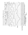
- Fig. 3 depicts how the output signal of each of the flip-flops 511 of the counter circuit 510 is updated as well as the voltage VCNT of the capacitor 540 is changed according to the logic level of the output signal of each of the flip-flops 511, in synchronization with the clock signal inputted from the FG circuit 600.
- the number of combinations of charging to the capacitor 540 are equal to the number of combinations of discharging from the capacitor 540, and thus the voltage VCNT of the capacitor 540 repeats a periodic change with the voltage of the predetermined level, set in advance, used as the reference (center), every time 12 pulses of the clock signal are inputted. That is, the voltage VCNT of the capacitor 540 returns to the original voltage every time 12 pulses of the clock signals are inputted.
- this reference voltage and the fluctuation range of the voltage are set in advance so that the output voltage outputted from the charge pump circuit 200 has a level within the range capable of turning on the transistor TR of the output circuit 400, which enable the output voltage from the charge pump circuit 200 not to deviate from the level capable of turning on the transistor TR of the output circuit 400.
- the fluctuation range of the voltage VCNT of the capacitor 540 can be set at a desired value by setting the capacitance of the capacitor 540, the current values of the current sources 520, the time period during which the switch 530 is on, the number (the number of stages) of the flip-flops 511 of the counter circuit 510, etc.
- the motor 700 makes one rotation every time 12 pulses (4 ⁇ 3) of the clock signal are inputted.
- the fluctuation cycle of the voltage VCNT with respect to one rotation of the motor 700 can be changed by changing the frequency of the clock signal.
- the oscillator circuit 100 is a circuit configured to output the oscillation signal of the switching speed corresponding to the level of the applied voltage VCNT that is outputted from the voltage changing circuit 500.
- the oscillator circuit 100 is configured as a ring oscillator includes an odd number of inverter circuits 111 that are ring-connected.
- Each of the inverter circuits 111 is configured as depicted in Fig. 5 , for example.
- the inverter circuit 111 is configured to output an output voltage Vout obtained by inverting the logic level of an input voltage Vin.
- the output voltage Vout is inverted and outputted after a predetermined delay.
- Each of the inverter circuits 111 is configured with a first NMOSFET 111A, a second NMOSFET 111B, a first PMOSFET 111C, and a second PMOSFET 111D.
- the gates of the first NMOSFET 111A and the first PMOSFET 111C are connected to each other and the drains of the first NMOSFET 111A and the first PMOSFET 111C are connected to each other. That is, the first NMOSFET 111A and the first PMOSFET 111C are connected so as to act as an inverter that inverts the input voltage Vin and outputs the output voltage Vout.
- the second NMOSFET 111B is connected in series between a power supply Vdd and the first NMOSFET 111A, and the second PMOSFET 111D is connected in series between the first PMOSFET 111C and the ground.
- a voltage VICNTp that changes with increase/decrease in the applied voltage VCNT is applied to the gate of the second NMOSFET 111B.
- a voltage VICNTn that changes with increase/decrease in the applied voltage VCNT in the direction opposite to the change in the voltage VICNTp is applied to the gate of the second PMOSFET 111D.
- the charging/discharging speed with respect to the parasitic capacitance, etc., in the inverter circuit 111 is decreased, resulting in increase in the delay time of the inverter circuit 111. That is, the response time, which is a time period from inverting of the input voltage Vin until inverting of the output voltage Vout is increased in level.
- the switching speed of the oscillation signal outputted from the oscillator circuit 100 changes with the level of the applied voltage VCNT outputted from the voltage changing circuit 500.
- This oscillation signal is inputted to the charge pump circuit 200 described above, and the transistors SW1 and SW2 configuring the charge pump circuit 200 repeat on and off in an alternate manner in synchronization with this oscillation signal.
- the load drive circuit 1000 according to an embodiment of the present invention, it is possible to change the switching speed of the oscillation signal inputted to the charge pump circuit 200.
- the frequency of the noise caused by this oscillation signal can be diffused, thereby being able to reduce the peak of the noise generated from the charge pump circuit 200.
- the oscillator circuit 100 can also be configured with a pseudo random number oscillator circuit capable of performing a pseudo random-number oscillation with respect to the switching frequency within a certain range, for example.
Landscapes
- Engineering & Computer Science (AREA)
- Power Engineering (AREA)
- Electronic Switches (AREA)
- Dc-Dc Converters (AREA)
- Inverter Devices (AREA)
Applications Claiming Priority (1)
| Application Number | Priority Date | Filing Date | Title |
|---|---|---|---|
| JP2012029868A JP2013169041A (ja) | 2012-02-14 | 2012-02-14 | 電圧出力回路 |
Publications (1)
| Publication Number | Publication Date |
|---|---|
| EP2629408A2 true EP2629408A2 (de) | 2013-08-21 |
Family
ID=47747422
Family Applications (1)
| Application Number | Title | Priority Date | Filing Date |
|---|---|---|---|
| EP20130154973 Withdrawn EP2629408A2 (de) | 2012-02-14 | 2013-02-12 | Spannungsausgabeschaltung, Lastantriebsschaltung und Verfahren zur Ausgabe von Spannung |
Country Status (3)
| Country | Link |
|---|---|
| US (1) | US9106165B2 (de) |
| EP (1) | EP2629408A2 (de) |
| JP (1) | JP2013169041A (de) |
Citations (1)
| Publication number | Priority date | Publication date | Assignee | Title |
|---|---|---|---|---|
| JP2009177894A (ja) | 2008-01-23 | 2009-08-06 | Rohm Co Ltd | モータ駆動装置、駆動方法およびそれを用いた冷却装置 |
Family Cites Families (5)
| Publication number | Priority date | Publication date | Assignee | Title |
|---|---|---|---|---|
| KR100264959B1 (ko) * | 1997-04-30 | 2000-10-02 | 윤종용 | 반도체 장치의 고전압발생회로 |
| US6084483A (en) * | 1999-03-10 | 2000-07-04 | Lexar Media, Inc. | Internal oscillator circuit including a ring oscillator controlled by a voltage regulator circuit |
| JP4394124B2 (ja) * | 2003-10-21 | 2010-01-06 | エヌエックスピー ビー ヴィ | チャージポンプ |
| JP2007251228A (ja) * | 2006-03-13 | 2007-09-27 | Toshiba Corp | 電圧制御発振器、動作電流調整装置、および、電圧制御発振器の動作電流調整方法 |
| JP2008005148A (ja) * | 2006-06-21 | 2008-01-10 | Nec Electronics Corp | スイッチ素子駆動回路および半導体装置 |
-
2012
- 2012-02-14 JP JP2012029868A patent/JP2013169041A/ja active Pending
-
2013
- 2013-02-12 EP EP20130154973 patent/EP2629408A2/de not_active Withdrawn
- 2013-02-13 US US13/766,109 patent/US9106165B2/en active Active
Patent Citations (1)
| Publication number | Priority date | Publication date | Assignee | Title |
|---|---|---|---|---|
| JP2009177894A (ja) | 2008-01-23 | 2009-08-06 | Rohm Co Ltd | モータ駆動装置、駆動方法およびそれを用いた冷却装置 |
Also Published As
| Publication number | Publication date |
|---|---|
| US9106165B2 (en) | 2015-08-11 |
| US20130207583A1 (en) | 2013-08-15 |
| JP2013169041A (ja) | 2013-08-29 |
Similar Documents
| Publication | Publication Date | Title |
|---|---|---|
| US8310188B2 (en) | Motor drive circuit with short startup time | |
| US8148928B2 (en) | Method for starting a brushless sensorless DC motor | |
| US9654040B2 (en) | Drive circuit of stepping motor, integrated circuit thereof, and electronic equipment including same, and method for controlling drive circuit of stepping motor | |
| US20100237813A1 (en) | Brushless motor driving apparatus | |
| US7492113B2 (en) | Brushless motor drive control circuit and brushless motor device using the same | |
| US9793839B2 (en) | Motor control circuit | |
| US20180019747A1 (en) | Signal transmission circuit and driving device for switching element | |
| US10050520B2 (en) | Charge pump circuit and motor thereof | |
| KR20110097672A (ko) | 모터 구동 회로 | |
| KR101063401B1 (ko) | 직류 모터 구동 회로 및 이를 포함하는 팬 모터 | |
| US9391548B2 (en) | Motor driving device for vehicle | |
| JPH10304698A (ja) | ステッピングモータ駆動装置 | |
| CN102280992B (zh) | 驱动电路、电源设备和包括其的电设备 | |
| JP2004304527A (ja) | ゲート駆動回路及びその電源制御方法 | |
| US20100237812A1 (en) | Motor driving apparatus | |
| US20070092232A1 (en) | Motor drive unit | |
| EP3226401A1 (de) | Motorantriebsvorrichtung | |
| JP6155179B2 (ja) | 整流装置、オルタネータおよび電力変換装置 | |
| US8963467B2 (en) | Motor driving device and method of controlling the same | |
| US9106165B2 (en) | Voltage output circuit, load drive circuit, and method for outputting voltage | |
| EP2306631A1 (de) | Antriebsvorrichtung für eine elektromagnetische Last und zugehöriges Verfahren | |
| US8648557B2 (en) | Drive control signal generating circuit | |
| US20220190690A1 (en) | Motor Driving Device | |
| CN107769671B (zh) | 用于运行电机的方法以及电机 | |
| KR20060115913A (ko) | 모터 드라이브 회로의 파워 트랜지스터 보호 회로, 모터드라이브 회로 및 반도체 장치 |
Legal Events
| Date | Code | Title | Description |
|---|---|---|---|
| PUAI | Public reference made under article 153(3) epc to a published international application that has entered the european phase |
Free format text: ORIGINAL CODE: 0009012 |
|
| AK | Designated contracting states |
Kind code of ref document: A2 Designated state(s): AL AT BE BG CH CY CZ DE DK EE ES FI FR GB GR HR HU IE IS IT LI LT LU LV MC MK MT NL NO PL PT RO RS SE SI SK SM TR |
|
| AX | Request for extension of the european patent |
Extension state: BA ME |
|
| STAA | Information on the status of an ep patent application or granted ep patent |
Free format text: STATUS: THE APPLICATION IS DEEMED TO BE WITHDRAWN |
|
| 18D | Application deemed to be withdrawn |
Effective date: 20150901 |