EP2629104A1 - Voltage monitoring device of plural assembly battery - Google Patents
Voltage monitoring device of plural assembly battery Download PDFInfo
- Publication number
- EP2629104A1 EP2629104A1 EP11832544.8A EP11832544A EP2629104A1 EP 2629104 A1 EP2629104 A1 EP 2629104A1 EP 11832544 A EP11832544 A EP 11832544A EP 2629104 A1 EP2629104 A1 EP 2629104A1
- Authority
- EP
- European Patent Office
- Prior art keywords
- voltage
- overcharge
- overdischarge
- signal
- cells
- Prior art date
- Legal status (The legal status is an assumption and is not a legal conclusion. Google has not performed a legal analysis and makes no representation as to the accuracy of the status listed.)
- Granted
Links
Images

Classifications
-
- G—PHYSICS
- G01—MEASURING; TESTING
- G01R—MEASURING ELECTRIC VARIABLES; MEASURING MAGNETIC VARIABLES
- G01R31/00—Arrangements for testing electric properties; Arrangements for locating electric faults; Arrangements for electrical testing characterised by what is being tested not provided for elsewhere
- G01R31/36—Arrangements for testing, measuring or monitoring the electrical condition of accumulators or electric batteries, e.g. capacity or state of charge [SoC]
- G01R31/382—Arrangements for monitoring battery or accumulator variables, e.g. SoC
- G01R31/3835—Arrangements for monitoring battery or accumulator variables, e.g. SoC involving only voltage measurements
-
- G—PHYSICS
- G01—MEASURING; TESTING
- G01R—MEASURING ELECTRIC VARIABLES; MEASURING MAGNETIC VARIABLES
- G01R31/00—Arrangements for testing electric properties; Arrangements for locating electric faults; Arrangements for electrical testing characterised by what is being tested not provided for elsewhere
- G01R31/36—Arrangements for testing, measuring or monitoring the electrical condition of accumulators or electric batteries, e.g. capacity or state of charge [SoC]
- G01R31/396—Acquisition or processing of data for testing or for monitoring individual cells or groups of cells within a battery
-
- G—PHYSICS
- G01—MEASURING; TESTING
- G01R—MEASURING ELECTRIC VARIABLES; MEASURING MAGNETIC VARIABLES
- G01R35/00—Testing or calibrating of apparatus covered by the other groups of this subclass
-
- H—ELECTRICITY
- H01—ELECTRIC ELEMENTS
- H01M—PROCESSES OR MEANS, e.g. BATTERIES, FOR THE DIRECT CONVERSION OF CHEMICAL ENERGY INTO ELECTRICAL ENERGY
- H01M10/00—Secondary cells; Manufacture thereof
- H01M10/42—Methods or arrangements for servicing or maintenance of secondary cells or secondary half-cells
- H01M10/425—Structural combination with electronic components, e.g. electronic circuits integrated to the outside of the casing
-
- H—ELECTRICITY
- H01—ELECTRIC ELEMENTS
- H01M—PROCESSES OR MEANS, e.g. BATTERIES, FOR THE DIRECT CONVERSION OF CHEMICAL ENERGY INTO ELECTRICAL ENERGY
- H01M10/00—Secondary cells; Manufacture thereof
- H01M10/42—Methods or arrangements for servicing or maintenance of secondary cells or secondary half-cells
- H01M10/48—Accumulators combined with arrangements for measuring, testing or indicating the condition of cells, e.g. the level or density of the electrolyte
- H01M10/482—Accumulators combined with arrangements for measuring, testing or indicating the condition of cells, e.g. the level or density of the electrolyte for several batteries or cells simultaneously or sequentially
-
- G—PHYSICS
- G01—MEASURING; TESTING
- G01R—MEASURING ELECTRIC VARIABLES; MEASURING MAGNETIC VARIABLES
- G01R19/00—Arrangements for measuring currents or voltages or for indicating presence or sign thereof
- G01R19/165—Indicating that current or voltage is either above or below a predetermined value or within or outside a predetermined range of values
- G01R19/16533—Indicating that current or voltage is either above or below a predetermined value or within or outside a predetermined range of values characterised by the application
- G01R19/16538—Indicating that current or voltage is either above or below a predetermined value or within or outside a predetermined range of values characterised by the application in AC or DC supplies
- G01R19/16542—Indicating that current or voltage is either above or below a predetermined value or within or outside a predetermined range of values characterised by the application in AC or DC supplies for batteries
-
- H—ELECTRICITY
- H01—ELECTRIC ELEMENTS
- H01M—PROCESSES OR MEANS, e.g. BATTERIES, FOR THE DIRECT CONVERSION OF CHEMICAL ENERGY INTO ELECTRICAL ENERGY
- H01M10/00—Secondary cells; Manufacture thereof
- H01M10/42—Methods or arrangements for servicing or maintenance of secondary cells or secondary half-cells
- H01M10/425—Structural combination with electronic components, e.g. electronic circuits integrated to the outside of the casing
- H01M2010/4278—Systems for data transfer from batteries, e.g. transfer of battery parameters to a controller, data transferred between battery controller and main controller
-
- H—ELECTRICITY
- H01—ELECTRIC ELEMENTS
- H01M—PROCESSES OR MEANS, e.g. BATTERIES, FOR THE DIRECT CONVERSION OF CHEMICAL ENERGY INTO ELECTRICAL ENERGY
- H01M2220/00—Batteries for particular applications
- H01M2220/20—Batteries in motive systems, e.g. vehicle, ship, plane
-
- Y—GENERAL TAGGING OF NEW TECHNOLOGICAL DEVELOPMENTS; GENERAL TAGGING OF CROSS-SECTIONAL TECHNOLOGIES SPANNING OVER SEVERAL SECTIONS OF THE IPC; TECHNICAL SUBJECTS COVERED BY FORMER USPC CROSS-REFERENCE ART COLLECTIONS [XRACs] AND DIGESTS
- Y02—TECHNOLOGIES OR APPLICATIONS FOR MITIGATION OR ADAPTATION AGAINST CLIMATE CHANGE
- Y02E—REDUCTION OF GREENHOUSE GAS [GHG] EMISSIONS, RELATED TO ENERGY GENERATION, TRANSMISSION OR DISTRIBUTION
- Y02E60/00—Enabling technologies; Technologies with a potential or indirect contribution to GHG emissions mitigation
- Y02E60/10—Energy storage using batteries
Definitions
- the present invention relates to a voltage monitoring apparatus to determine whether or not each cell voltage is normal in a plural battery that connects a plurality of unit cells in series to output a required voltage.
- an electric car or a hybrid vehicle has a high-voltage battery as a power source for driving a motor.
- a high-voltage battery connects a plurality of unit cells of a secondary battery (rechargeable battery) such as a nickel-hydrogen battery and a lithium battery in series to provide a high voltage.
- a secondary battery rechargeable battery
- Each unit cell of the secondary battery is charged with the same power and is discharged at the same power. Accordingly, if the unit cells differently deteriorate, the secondary battery will easily get an overcharge or overdischarge state. To prevent the overcharge or overdischarge state of the secondary battery, the charging state of each unit cell must be checked.
- a plurality of unit cells for example, fifty five unit cells are divided into, for example, five blocks (namely, eleven unit cells per block) and the voltage of each block is measured in real time with a voltage detecting IC provided for each block, to monitor if the voltage is abnormal.
- the voltage detecting IC measures the voltage of each of the unit cells (for example, 11 cells) contained in the block and converts a measured analog voltage signal into a digital signal with an A/D converter provided for the voltage detecting IC.
- the digitized measured voltage is compared with upper and lower thresholds of cell voltage, and if the measured voltage is equal to or greater than the upper threshold, it is determined to be overcharge. If the measured voltage is equal to or lower than the lower threshold, it is determined to be overdischarge.
- a related art is disclosed in, for example, Japanese Unexamined Patent Application Publication No. 2010-35337 . Thereafter, the determination result is transmitted as a digital fail signal to a microcomputer on a low-voltage side, so that the microcomputer may recognize the cell voltage abnormality.
- the voltage monitoring apparatus transmits the digital fail signal from the voltage detecting IC to the microcomputer, to inform of an occurrence of overcharge or overdischarge. Accordingly, if a communication line of the digital signal causes a communication error, a problem arises that the occurrence of overcharge or overdischarge is not correctly informed to the microcomputer side.
- the present invention has been made to solve such a problem and provides a voltage monitoring apparatus for a plural battery, capable of surely transmitting overcharge or overdischarge data detected by a voltage abnormality detecting unit to a monitoring apparatus side.
- a voltage monitoring apparatus for a plural battery that connects a plurality of cells in series to output a required voltage.
- the apparatus monitors an abnormality in an output voltage of each of the cells and includes a voltage abnormality detecting unit provided for each of a plurality of blocks into which the plurality of cells are divided.
- the voltage abnormality detecting unit detects a voltage abnormality in each of the cells contained in the block and includes a voltage detector that detects a cell voltage of each of the cells contained in the block, a comparator that compares the cell voltage detected by the voltage detector with preset upper and lower thresholds and determines whether or not the cell voltage is overcharge or overdischarge, and a transmitter that transmits the determination result of the comparator as a digital determination signal and an analog determination signal.
- the apparatus also includes a monitoring unit that determines, according to the digital determination signal and analog determination signal, whether or not the individual voltage abnormality detecting units are normally operating.
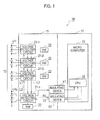
- Figure 1 is a block diagram illustrating a voltage monitoring apparatus 10 according to the embodiment of the present invention and a secondary battery (plural battery) 13 including a plurality of unit cells BT1 to BT55.
- Figure 2 is a block diagram illustrating a detailed configuration of a first voltage detecting IC (21-1).
- the secondary battery 13 adopted by this embodiment is used as, for example, a high-voltage battery to drive a motor of an electric car, a hybrid vehicle, or the like.
- the voltage monitoring apparatus 10 is separated by insulating devices 41 and 42 into a high-voltage side 11 and a low-voltage side 12.
- the low-voltage side 12 includes a microcomputer 31 such as a microcontroller having a CPU (monitoring unit) 32.
- the CPU 32 receives unit-cell voltages detected by the voltage detecting ICs (21-1) to (21-n) of the high-voltage side 11, displays the unit-cell voltages on a display unit (not illustrated) and the like, and informs of an overcharge or overdischarge state of the unit-cell voltages according to overcharge and overdischarge data (fail signal) transmitted from the voltage detecting ICs (21-1) to (21-n).
- Each of the voltage detecting ICs (21-1) to (21-n) has an AD converter (A/D converting unit) 26 (refer to Fig. 2 ) to convert cell voltages (an analog voltage signal) of the voltage detecting IC into a digital voltage signal with the use of an A/D conversion voltage Vref provided by a reference power source 22.
- AD converter A/D converting unit
- Adjacent ones of the voltage detecting ICs (21-1) to (21-n) are connected to each other through digital communication lines L1 and L2.
- the voltage detecting ICs are connected through the insulating device 42 to the microcomputer 31. Accordingly, a TX signal, such as a voltage detection instructing signal, outputted from the microcomputer 31 is transmitted through daisy-chain communication to the voltage detecting ICs (21-1) to (21-n) and an RX signal, such as a fail signal indicative of overcharge or overdischarge, outputted from the voltage detecting ICs (21-1) to (21-n) is transmitted through the daisy-chain communication to the microcomputer 31.
- Adjacent ones of the voltage detecting ICs (21-1) to (21-n) are connected to each other through a communication line L3 and are also connected through the insulating device 41 to the CPU 32 of the microcomputer 31.
- the first voltage detecting IC (21-1) includes a multiplexer 51 that is connected to a plurality of unit cells BT1 to BT11 (the number of cells is assumed to be eleven as an example), detects output power of the unit cells, and converts detected voltage signals of the unit cells BT1 to BT11 into a single time-series signal, an AD converter 52 that digitizes the voltage signal (analog signal) outputted from the multiplexer 51, and a cell voltage memory 53 that stores the digitized voltage signal from the AD converter 52.
- a threshold memory 55 that stores an upper threshold to determine overcharge of cell voltage and a lower threshold to determine overdischarge of cell voltage
- a comparator 54 that compares the cell voltages of the unit cells BT1 to BT11 with the upper and lower thresholds stored in the threshold memory 55
- a determination result register 56 that stores a determination result from the comparator 54
- a DA converter 57 that stores a digital communication circuit 58.
- the determination result register 56 determines that, if the cell voltage of a given unit cell is equal to or greater than the upper threshold, the unit cell is in an overcharge state and that, if the cell voltage is equal to or lower than the lower threshold, the unit cell is in an overdischarge state and stores the determination result.
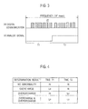
- the DA converter 57 converts the determination result data (digital signal) stored in the determination result register 56 into an analog signal and transmits the analog signal through the analog communication line L3 and insulating device 41 illustrated in Fig. 1 to the CPU 32 of the microcomputer 31. At this time, the DA converter 57 divides a communication period of X (ms) into time T1 and T2 as illustrated in Fig. 3(b) , and according to a combination of output levels "Hi" and "Lo" in the time T1 and T2, generates a signal (fail signal) indicating overcharge or overdischarge.
- this embodiment indicates no abnormality if the time T1 and T2 are both Hi, an occurrence of overcharge if the time T1 is Lo and the Time T2 is Hi, an occurrence of overdischarge if the time T1 is Hi and time T2 is Lo, and an occurrence of both the overcharge and overdischarge if the time T1 and T2 are both Lo.
- the technique of configuring the fail signal is not limited to the example illustrated in Fig. 4 .
- the digital communication circuit 58 employs a predetermined digital communication method to transmit the voltage data stored in the cell voltage memory 53 and the determination result data stored in the determination result register 56 at intervals of the communication period of X (ms).
- a digital signal that changes between logic levels of "1" and "0" as illustrated in Fig. 3(a) is transmitted through the digital communication line L2 and insulating device 42 illustrated in Fig. 1 to the CPU 32 of the microcomputer 31.
- data "d1" in the data string illustrated in Fig. 3 (a) is used as a signal (fail signal) indicating the overcharge or overdischarge of the unit cells BT1 to BT11.
- the CPU 32 transmits at the predetermined intervals of X (ms) a voltage detection instructing signal through the insulating device 42 and digital communication line L1 to the voltage detecting ICs (21-1) to (21-n).
- each of the voltage detecting ICs (21-1) to (21-n) digitizes voltages of the unit cells BT1 to BT11 by the AD converter 52 and stores a digitized voltage signal in the cell voltage memory 53. Thereafter, the comparator 54 compares the voltage signal of the unit cells BT1 to BT11 stored in the cell voltage memory 53 with the upper and lower thresholds stored in the threshold memory 55 and determines whether the voltage of each of the unit cells BT1 to BT11 is overcharge i.e. whether the voltage is equal to or greater than the upper threshold, or overdischarge i.e. whether the voltage is equal to or lower than the lower threshold.
- the determination result is once stored in the determination result register 56, and thereafter, is outputted to the DA converter 57 and digital communication circuit 58.
- the DA converter According to the overcharge or overdischarge state data of each of the unit cells BT1 to BT11 in the determination result register 56, the DA converter generates a fail signal having two levels "Hi” and "Lo” as illustrated in Fig. 3(b) .
- the time T1 and T2 are both set to "Hi"
- the time T1 is set to "Lo” and time T2 to "Hi”
- the time T1 is set to "Hi” and the time T2 to "Lo”
- the time T1 and T2 are both set to "Lo”.
- the fail signal is transmitted through the analog communication line L3 and insulating device 41 to the CPU 32.
- the digital communication circuit 58 employs the predetermined digital communication method and transmits the voltage signal stored in the cell voltage memory 53 and the fail signal stored in the determination result register 56 through the digital communication line L2 and insulating device 41 to the CPU 32.
- the CPU 32 receives the analog fail signal transmitted through the analog communication line L3 and the digital fail signal transmitted through the digital communication line L2, and according to both the fail signals, determines whether or not the unit cells connected to the voltage detecting ICs (21-1) to (21-n) are overcharge or overdischarge. This determination process determines overcharge or overdischarge when the analog fail signal and digital fail signal agree with each other. If the fail signals disagree with each other, it is determined that a communication error is occurring and inform an operator of the error with an alarm signal or the like. Accordingly, even if the communication lines L1 to L3 cause an abnormality, the embodiment can surely detect the overcharge or overdischarge of each unit cell.
- the voltage monitoring apparatus 10 transmits, in both digital and analog signals, a fail signal indicating overcharge or overdischarge of the unit cells detected by the voltage detecting ICs (21-1) to (21-n) to the CPU 32. If the analog fail signal and digital fail signal agree with each other, the CPU 32 determines that the unit cells are causing overcharge or overdischarge. If the fail signals disagree with each other, it is determined that an error is occurring in data communication in the communication lines L1 to L3 and the error is informed to an operator with an alarm signal or the line.
- the embodiment surely recognizes an occurrence of overcharge or overdischarge of the unit cells and remarkably improves an overcharge/overdischarge detecting accuracy.
- the embodiment is capable of immediately inform an operator of a communication error occurring in the communication lines L1 to L3.
- This embodiment uses, in addition to usual communication with digital signals, an analog fail signal instead of providing the digital signals with redundancy. Accordingly, the embodiment is capable of reducing a circuit scale and suppressing a cost increase.
- the voltage monitoring apparatus for a plural battery converts a fail signal indicating overcharge or overdischarge of the unit cells detected by the voltage abnormality detecting units such as the voltage detecting ICs (21-1) to (21-n) into a digital signal and an analog signal and transmits both the analog fail signal and digital fail signal to the monitoring unit such as the CPU 32. If the analog fail signal and digital fail signal agree with each other, the monitoring unit determines that the unit cells are causing overcharge or overdischarge. If both the signals disagree with each other, it is determined that a communication error is occurring in the communication line such as the communication lines L1 to L3 connecting the voltage abnormality detecting units and monitoring unit to each other.
- the present invention is capable of surely recognizing the occurrence of overcharge or overdischarge in the unit cells and remarkably improving an overcharge/overdischarge detecting accuracy.
- the present invention is capable of immediately recognizing the occurrence of a communication error in the communication lines, if any.
- the present invention is very useful in highly accurately detecting overcharge or overdischarge of unit cells arranged in a plural battery.
Landscapes
- Physics & Mathematics (AREA)
- General Physics & Mathematics (AREA)
- Engineering & Computer Science (AREA)
- Manufacturing & Machinery (AREA)
- Chemical & Material Sciences (AREA)
- Chemical Kinetics & Catalysis (AREA)
- Electrochemistry (AREA)
- General Chemical & Material Sciences (AREA)
- Microelectronics & Electronic Packaging (AREA)
- Secondary Cells (AREA)
- Tests Of Electric Status Of Batteries (AREA)
- Charge And Discharge Circuits For Batteries Or The Like (AREA)
Abstract
Description
- The present invention relates to a voltage monitoring apparatus to determine whether or not each cell voltage is normal in a plural battery that connects a plurality of unit cells in series to output a required voltage.
- For example, an electric car or a hybrid vehicle has a high-voltage battery as a power source for driving a motor. Such a high-voltage battery connects a plurality of unit cells of a secondary battery (rechargeable battery) such as a nickel-hydrogen battery and a lithium battery in series to provide a high voltage.
- Each unit cell of the secondary battery is charged with the same power and is discharged at the same power. Accordingly, if the unit cells differently deteriorate, the secondary battery will easily get an overcharge or overdischarge state. To prevent the overcharge or overdischarge state of the secondary battery, the charging state of each unit cell must be checked.
- Previously, a plurality of unit cells (for example, fifty five unit cells) are divided into, for example, five blocks (namely, eleven unit cells per block) and the voltage of each block is measured in real time with a voltage detecting IC provided for each block, to monitor if the voltage is abnormal.
- At this time, the voltage detecting IC measures the voltage of each of the unit cells (for example, 11 cells) contained in the block and converts a measured analog voltage signal into a digital signal with an A/D converter provided for the voltage detecting IC. The digitized measured voltage is compared with upper and lower thresholds of cell voltage, and if the measured voltage is equal to or greater than the upper threshold, it is determined to be overcharge. If the measured voltage is equal to or lower than the lower threshold, it is determined to be overdischarge. A related art is disclosed in, for example, Japanese Unexamined Patent Application Publication No.
2010-35337 - The voltage monitoring apparatus according to the related art, however, transmits the digital fail signal from the voltage detecting IC to the microcomputer, to inform of an occurrence of overcharge or overdischarge. Accordingly, if a communication line of the digital signal causes a communication error, a problem arises that the occurrence of overcharge or overdischarge is not correctly informed to the microcomputer side.
- The present invention has been made to solve such a problem and provides a voltage monitoring apparatus for a plural battery, capable of surely transmitting overcharge or overdischarge data detected by a voltage abnormality detecting unit to a monitoring apparatus side.
- According to a technical aspect of the present invention, there is provided a voltage monitoring apparatus for a plural battery that connects a plurality of cells in series to output a required voltage. The apparatus monitors an abnormality in an output voltage of each of the cells and includes a voltage abnormality detecting unit provided for each of a plurality of blocks into which the plurality of cells are divided. The voltage abnormality detecting unit detects a voltage abnormality in each of the cells contained in the block and includes a voltage detector that detects a cell voltage of each of the cells contained in the block, a comparator that compares the cell voltage detected by the voltage detector with preset upper and lower thresholds and determines whether or not the cell voltage is overcharge or overdischarge, and a transmitter that transmits the determination result of the comparator as a digital determination signal and an analog determination signal. The apparatus also includes a monitoring unit that determines, according to the digital determination signal and analog determination signal, whether or not the individual voltage abnormality detecting units are normally operating.
-
-
Figure 1 is a block diagram illustrating a configuration of a voltage monitoring apparatus for a plural battery according to an embodiment of the present invention. -
Figure 2 is a block diagram illustrating a detailed configuration of a voltage detecting IC arranged in the voltage monitoring apparatus for a plural battery according to the embodiment of the present invention. -
Figure 3 is a waveform diagram illustrating a digital signal and an analog signal transmitted from the voltage detecting IC of the voltage monitoring apparatus for a plural battery according to the embodiment of the present invention. -
Figure 4 is an explanatory view illustrating the details of the analog signal transmitted from the voltage detecting IC of the voltage monitoring apparatus for a plural battery according to the embodiment of the present invention. - An embodiment of the present invention will be explained with reference to the drawings.
Figure 1 is a block diagram illustrating avoltage monitoring apparatus 10 according to the embodiment of the present invention and a secondary battery (plural battery) 13 including a plurality of unit cells BT1 to BT55.Figure 2 is a block diagram illustrating a detailed configuration of a first voltage detecting IC (21-1). Thesecondary battery 13 adopted by this embodiment is used as, for example, a high-voltage battery to drive a motor of an electric car, a hybrid vehicle, or the like. - As illustrated in
Fig. 1 , thevoltage monitoring apparatus 10 according to the embodiment is separated byinsulating devices 41 and 42 into a high-voltage side 11 and a low-voltage side 12. - The high-
voltage side 11 includes n voltage detecting ICs, i.e., a first voltage detecting IC (21-1) to an n-th voltage detecting IC (21-n). Each of the voltage detecting ICs (21-1) to (21-n) is a voltage abnormality detecting unit that is connected to a plurality of unit cells to measure a voltage of each of the unit cells. - The low-
voltage side 12 includes amicrocomputer 31 such as a microcontroller having a CPU (monitoring unit) 32. TheCPU 32 receives unit-cell voltages detected by the voltage detecting ICs (21-1) to (21-n) of the high-voltage side 11, displays the unit-cell voltages on a display unit (not illustrated) and the like, and informs of an overcharge or overdischarge state of the unit-cell voltages according to overcharge and overdischarge data (fail signal) transmitted from the voltage detecting ICs (21-1) to (21-n). - Each of the voltage detecting ICs (21-1) to (21-n) has an AD converter (A/D converting unit) 26 (refer to
Fig. 2 ) to convert cell voltages (an analog voltage signal) of the voltage detecting IC into a digital voltage signal with the use of an A/D conversion voltage Vref provided by areference power source 22. - Adjacent ones of the voltage detecting ICs (21-1) to (21-n) are connected to each other through digital communication lines L1 and L2. In addition, the voltage detecting ICs are connected through the
insulating device 42 to themicrocomputer 31. Accordingly, a TX signal, such as a voltage detection instructing signal, outputted from themicrocomputer 31 is transmitted through daisy-chain communication to the voltage detecting ICs (21-1) to (21-n) and an RX signal, such as a fail signal indicative of overcharge or overdischarge, outputted from the voltage detecting ICs (21-1) to (21-n) is transmitted through the daisy-chain communication to themicrocomputer 31. - Adjacent ones of the voltage detecting ICs (21-1) to (21-n) are connected to each other through a communication line L3 and are also connected through the insulating device 41 to the
CPU 32 of themicrocomputer 31. - With reference to
Fig. 2 , the detailed configuration of each of the voltage detecting ICs (21-1) to (21-n) will be explained. Here, the first voltage detecting IC (21-1) will be explained as an example. - As illustrated in
Fig. 2 , the first voltage detecting IC (21-1) includes amultiplexer 51 that is connected to a plurality of unit cells BT1 to BT11 (the number of cells is assumed to be eleven as an example), detects output power of the unit cells, and converts detected voltage signals of the unit cells BT1 to BT11 into a single time-series signal, anAD converter 52 that digitizes the voltage signal (analog signal) outputted from themultiplexer 51, and acell voltage memory 53 that stores the digitized voltage signal from theAD converter 52. - Also included are a
threshold memory 55 that stores an upper threshold to determine overcharge of cell voltage and a lower threshold to determine overdischarge of cell voltage, acomparator 54 that compares the cell voltages of the unit cells BT1 to BT11 with the upper and lower thresholds stored in thethreshold memory 55, adetermination result register 56 that stores a determination result from thecomparator 54, aDA converter 57, and adigital communication circuit 58. - The
determination result register 56 determines that, if the cell voltage of a given unit cell is equal to or greater than the upper threshold, the unit cell is in an overcharge state and that, if the cell voltage is equal to or lower than the lower threshold, the unit cell is in an overdischarge state and stores the determination result. - The
DA converter 57 converts the determination result data (digital signal) stored in thedetermination result register 56 into an analog signal and transmits the analog signal through the analog communication line L3 and insulating device 41 illustrated inFig. 1 to theCPU 32 of themicrocomputer 31. At this time, theDA converter 57 divides a communication period of X (ms) into time T1 and T2 as illustrated inFig. 3(b) , and according to a combination of output levels "Hi" and "Lo" in the time T1 and T2, generates a signal (fail signal) indicating overcharge or overdischarge. - As illustrated in
Fig. 4 , this embodiment indicates no abnormality if the time T1 and T2 are both Hi, an occurrence of overcharge if the time T1 is Lo and the Time T2 is Hi, an occurrence of overdischarge if the time T1 is Hi and time T2 is Lo, and an occurrence of both the overcharge and overdischarge if the time T1 and T2 are both Lo. The technique of configuring the fail signal is not limited to the example illustrated inFig. 4 . - The
digital communication circuit 58 employs a predetermined digital communication method to transmit the voltage data stored in thecell voltage memory 53 and the determination result data stored in thedetermination result register 56 at intervals of the communication period of X (ms). As a result, a digital signal that changes between logic levels of "1" and "0" as illustrated inFig. 3(a) is transmitted through the digital communication line L2 andinsulating device 42 illustrated inFig. 1 to theCPU 32 of themicrocomputer 31. For example, data "d1" in the data string illustrated inFig. 3 (a) is used as a signal (fail signal) indicating the overcharge or overdischarge of the unit cells BT1 to BT11. - Operation of the voltage monitoring apparatus according to the embodiment with the above-mentioned structure will be explained. First, the
CPU 32 transmits at the predetermined intervals of X (ms) a voltage detection instructing signal through theinsulating device 42 and digital communication line L1 to the voltage detecting ICs (21-1) to (21-n). - Receiving the voltage detection instructing signal, each of the voltage detecting ICs (21-1) to (21-n) digitizes voltages of the unit cells BT1 to BT11 by the
AD converter 52 and stores a digitized voltage signal in thecell voltage memory 53. Thereafter, thecomparator 54 compares the voltage signal of the unit cells BT1 to BT11 stored in thecell voltage memory 53 with the upper and lower thresholds stored in thethreshold memory 55 and determines whether the voltage of each of the unit cells BT1 to BT11 is overcharge i.e. whether the voltage is equal to or greater than the upper threshold, or overdischarge i.e. whether the voltage is equal to or lower than the lower threshold. - The determination result is once stored in the
determination result register 56, and thereafter, is outputted to theDA converter 57 anddigital communication circuit 58. - According to the overcharge or overdischarge state data of each of the unit cells BT1 to BT11 in the
determination result register 56, the DA converter generates a fail signal having two levels "Hi" and "Lo" as illustrated inFig. 3(b) . For example, if all of the unit cells BT1 to BT11 have a normal voltage, the time T1 and T2 are both set to "Hi", if at least one of the unit cells BT1 to BT11 is overcharge and there is no unit cell of overdischarge, the time T1 is set to "Lo" and time T2 to "Hi", if at least one of the unit cells BT1 to BT11 is overdischarge and there is no unit cell of overcharge, the time T1 is set to "Hi" and the time T2 to "Lo", and if at least one of the unit cells BT1 to BT11 is overcharge and at least one of them overdischarge, the time T1 and T2 are both set to "Lo". - The fail signal is transmitted through the analog communication line L3 and insulating device 41 to the
CPU 32. - On the other hand, the
digital communication circuit 58 employs the predetermined digital communication method and transmits the voltage signal stored in thecell voltage memory 53 and the fail signal stored in thedetermination result register 56 through the digital communication line L2 and insulating device 41 to theCPU 32. - The
CPU 32 receives the analog fail signal transmitted through the analog communication line L3 and the digital fail signal transmitted through the digital communication line L2, and according to both the fail signals, determines whether or not the unit cells connected to the voltage detecting ICs (21-1) to (21-n) are overcharge or overdischarge. This determination process determines overcharge or overdischarge when the analog fail signal and digital fail signal agree with each other. If the fail signals disagree with each other, it is determined that a communication error is occurring and inform an operator of the error with an alarm signal or the like. Accordingly, even if the communication lines L1 to L3 cause an abnormality, the embodiment can surely detect the overcharge or overdischarge of each unit cell. - In this way, the
voltage monitoring apparatus 10 according to the embodiment transmits, in both digital and analog signals, a fail signal indicating overcharge or overdischarge of the unit cells detected by the voltage detecting ICs (21-1) to (21-n) to theCPU 32. If the analog fail signal and digital fail signal agree with each other, theCPU 32 determines that the unit cells are causing overcharge or overdischarge. If the fail signals disagree with each other, it is determined that an error is occurring in data communication in the communication lines L1 to L3 and the error is informed to an operator with an alarm signal or the line. - Accordingly, the embodiment surely recognizes an occurrence of overcharge or overdischarge of the unit cells and remarkably improves an overcharge/overdischarge detecting accuracy. In addition, the embodiment is capable of immediately inform an operator of a communication error occurring in the communication lines L1 to L3.
- This embodiment uses, in addition to usual communication with digital signals, an analog fail signal instead of providing the digital signals with redundancy. Accordingly, the embodiment is capable of reducing a circuit scale and suppressing a cost increase.
- Although the voltage monitoring apparatus for a plural battery according to the present invention has been explained with reference to the embodiment illustrated in the drawings, the present invention is not limited to the embodiment. The configuration of each part of the embodiment is replaceable with any configuration that may provide the same or similar function.
- The voltage monitoring apparatus for a plural battery according to the present invention converts a fail signal indicating overcharge or overdischarge of the unit cells detected by the voltage abnormality detecting units such as the voltage detecting ICs (21-1) to (21-n) into a digital signal and an analog signal and transmits both the analog fail signal and digital fail signal to the monitoring unit such as the
CPU 32. If the analog fail signal and digital fail signal agree with each other, the monitoring unit determines that the unit cells are causing overcharge or overdischarge. If both the signals disagree with each other, it is determined that a communication error is occurring in the communication line such as the communication lines L1 to L3 connecting the voltage abnormality detecting units and monitoring unit to each other. - Accordingly, the present invention is capable of surely recognizing the occurrence of overcharge or overdischarge in the unit cells and remarkably improving an overcharge/overdischarge detecting accuracy. In addition, the present invention is capable of immediately recognizing the occurrence of a communication error in the communication lines, if any.
- The present invention is very useful in highly accurately detecting overcharge or overdischarge of unit cells arranged in a plural battery.
- In connection with United States designation, this international patent application claims the benefit of priority under 35 U.S.C. 119(a) to Japanese Patent Application No.
2010-231205 filed on October 14, 2010
Claims (4)
- A voltage monitoring apparatus for a plural battery, the plural battery outputting a required voltage and connecting a plurality of cells in series, and the apparatus monitoring an abnormality in an output voltage of each of the cells, the apparatus comprising:a voltage abnormality detector provided for each of a plurality of blocks into which the plurality of cells are divided, the voltage abnormality detector detecting a voltage abnormality in each of the cells contained in the block, the voltage abnormality detector including:a voltage detector detecting a cell voltage of each of the cells contained in the block;a comparator comparing the cell voltage detected by the voltage detector with preset upper and lower thresholds and determining whether or not the cell voltage is overcharge or overdischarge; anda transmitter transmitting the determination result of the comparator by way of a digital determination signal and an analog determination signal; anda monitoring unit determining whether or not the individual voltage abnormality detector are normally operating according to the digital determination signal and analog determination signal.
- The voltage monitoring apparatus for a plural battery according to claim 1, wherein
the monitoring unit confirms whether information about overcharge and overdischarge of the cells derived from the digital determination signal agrees or disagrees with information about overcharge and overdischarge of the cells derived from the analog determination signal, and
based on the confirmation, determines whether or not a communication error is occurring in a communication line between the voltage abnormality detector and the monitoring unit. - The voltage monitoring apparatus for a plural battery according to claim 2, wherein
the monitoring unit outputs an alarm signal if the information about overcharge and overdischarge of the cells derived from the digital determination signal disagrees with the information about overcharge and overdischarge of the cells derived from the analog determination signal. - The voltage monitoring apparatus for a plural battery according to any one of claims 1 to 3, wherein
the voltage abnormality detector are arranged in a high-voltage-side circuit and the monitoring unit is arranged in a low-voltage-side circuit that is connected through an insulating interface to the high-voltage-side circuit.
Applications Claiming Priority (2)
| Application Number | Priority Date | Filing Date | Title |
|---|---|---|---|
| JP2010231205A JP5670693B2 (en) | 2010-10-14 | 2010-10-14 | Battery voltage monitoring device |
| PCT/JP2011/073383 WO2012050109A1 (en) | 2010-10-14 | 2011-10-12 | Voltage monitoring device of plural assembly battery |
Publications (3)
| Publication Number | Publication Date |
|---|---|
| EP2629104A1 true EP2629104A1 (en) | 2013-08-21 |
| EP2629104A4 EP2629104A4 (en) | 2017-12-27 |
| EP2629104B1 EP2629104B1 (en) | 2023-02-22 |
Family
ID=45938338
Family Applications (1)
| Application Number | Title | Priority Date | Filing Date |
|---|---|---|---|
| EP11832544.8A Active EP2629104B1 (en) | 2010-10-14 | 2011-10-12 | Voltage monitoring device of plural assembly battery |
Country Status (5)
| Country | Link |
|---|---|
| US (1) | US9335381B2 (en) |
| EP (1) | EP2629104B1 (en) |
| JP (1) | JP5670693B2 (en) |
| CN (1) | CN103154748B (en) |
| WO (1) | WO2012050109A1 (en) |
Cited By (3)
| Publication number | Priority date | Publication date | Assignee | Title |
|---|---|---|---|---|
| FR3042282A1 (en) * | 2015-10-12 | 2017-04-14 | Commissariat Energie Atomique | ELECTRONIC SYSTEM FOR CONTROLLING AN ELECTRIC BATTERY |
| EP3043441B1 (en) * | 2014-01-27 | 2019-12-18 | LG Chem, Ltd. | Battery management unit for preventing performance of erroneous control algorithm from communication error |
| EP3174176B1 (en) * | 2015-11-30 | 2020-03-11 | Makita Corporation | Battery device and charging device |
Families Citing this family (13)
| Publication number | Priority date | Publication date | Assignee | Title |
|---|---|---|---|---|
| JP2014082152A (en) * | 2012-10-18 | 2014-05-08 | Yazaki Corp | Voltage detection device |
| JP5713094B2 (en) * | 2013-06-06 | 2015-05-07 | 株式会社豊田自動織機 | Battery monitoring device |
| DE102013215968A1 (en) * | 2013-08-13 | 2015-03-12 | Robert Bosch Gmbh | Electromechanical adapter |
| CN105762870A (en) * | 2016-03-30 | 2016-07-13 | 合肥联宝信息技术有限公司 | Battery having protection and early warning functions and electronic equipment having the battery |
| CN107703350A (en) * | 2017-09-07 | 2018-02-16 | 上海斐讯数据通信技术有限公司 | The voltage monitoring system and method for a kind of equipment |
| KR102474424B1 (en) | 2017-10-31 | 2022-12-05 | 주식회사 엘엑스세미콘 | Communication method between master controller and slave controller, the slave controller for the same, and battery management system using the same |
| CN109407009A (en) * | 2018-11-16 | 2019-03-01 | 国网江苏省电力有限公司盐城供电分公司 | A kind of battery group on-line detecting system and its detection method based on multi-signal acquisition |
| HUE061832T2 (en) * | 2020-07-02 | 2023-08-28 | Contemporary Amperex Technology Co Ltd | Battery state estimation method and apparatus, and device, battery system and storage medium |
| KR102786688B1 (en) * | 2020-07-24 | 2025-03-25 | 주식회사 엘지에너지솔루션 | Fault cell diagnosis method and battery system using the same |
| ES2910101B2 (en) * | 2020-11-11 | 2023-07-17 | Caf Power & Automation S L U | ELECTRICAL ENERGY ACCUMULATION SYSTEM |
| CN112540218A (en) * | 2020-12-07 | 2021-03-23 | 上海卫星工程研究所 | Satellite final assembly integrated test factory building dress star lithium cell group under-voltage alarm device |
| CN117207844B (en) * | 2023-10-08 | 2024-10-01 | 赛力斯汽车有限公司 | A dynamic alarm method, device, equipment and storage medium |
| CN120275844B (en) * | 2025-06-10 | 2025-09-19 | 重庆长安汽车股份有限公司 | Battery pack overcharging diagnosis method, overdischarging diagnosis method and device |
Family Cites Families (18)
| Publication number | Priority date | Publication date | Assignee | Title |
|---|---|---|---|---|
| JPS63141101A (en) * | 1986-12-03 | 1988-06-13 | Fuji Electric Co Ltd | Redundancy controller |
| US5440585A (en) * | 1993-06-14 | 1995-08-08 | At&T Corp. | Applications of simultaneous analog and digital communication |
| US6060864A (en) * | 1994-08-08 | 2000-05-09 | Kabushiki Kaisha Toshiba | Battery set structure and charge/discharge control apparatus for lithium-ion battery |
| JPH11205217A (en) * | 1998-01-07 | 1999-07-30 | Toshiba Corp | Dual mode wireless communication device having function of selectively using analog mode and digital mode |
| JP2002365038A (en) * | 2001-06-07 | 2002-12-18 | Mitsutoyo Corp | Digital and analog joint display measuring device |
| JP4287077B2 (en) * | 2001-07-12 | 2009-07-01 | 株式会社デンソー | Charge state detection device |
| JP4196250B2 (en) * | 2001-09-18 | 2008-12-17 | 株式会社デンソー | Battery pack control device |
| JP2005318751A (en) * | 2004-04-30 | 2005-11-10 | Shin Kobe Electric Mach Co Ltd | Multi-series battery control system |
| US7521896B2 (en) * | 2004-07-20 | 2009-04-21 | Panasonic Ev Energy Co., Ltd. | Abnormal voltage detector apparatus for detecting voltage abnormality in assembled battery |
| JP2006062482A (en) * | 2004-08-25 | 2006-03-09 | Honda Motor Co Ltd | Remote control device for outboard motor |
| JP2006064639A (en) * | 2004-08-30 | 2006-03-09 | Renesas Technology Corp | Cell voltage monitoring device |
| JP4858378B2 (en) * | 2007-09-14 | 2012-01-18 | 日本テキサス・インスツルメンツ株式会社 | Cell voltage monitoring device for multi-cell series batteries |
| JP5250230B2 (en) * | 2007-09-28 | 2013-07-31 | 株式会社日立製作所 | Power supply system for vehicle and integrated circuit for battery cell control |
| CN100574915C (en) * | 2007-12-14 | 2009-12-30 | 苏州有色金属研究院有限公司 | Method of Improving Thickness Control Performance of Cold Rolling Mill Using Feedforward Network |
| JP5386872B2 (en) * | 2008-07-29 | 2014-01-15 | 株式会社デンソー | Battery monitoring and control device |
| DE102008057474B4 (en) * | 2008-11-14 | 2012-08-02 | Kg Transmitter Components Gmbh | transmitters |
| JP5386155B2 (en) * | 2008-11-28 | 2014-01-15 | 株式会社日立製作所 | Power storage device |
| CN101847376B (en) | 2009-03-25 | 2013-10-30 | 北京京东方光电科技有限公司 | Common electrode driving circuit and LCD |
-
2010
- 2010-10-14 JP JP2010231205A patent/JP5670693B2/en active Active
-
2011
- 2011-10-12 WO PCT/JP2011/073383 patent/WO2012050109A1/en not_active Ceased
- 2011-10-12 EP EP11832544.8A patent/EP2629104B1/en active Active
- 2011-10-12 CN CN201180049787.5A patent/CN103154748B/en active Active
-
2013
- 2013-04-10 US US13/859,953 patent/US9335381B2/en active Active
Non-Patent Citations (1)
| Title |
|---|
| See references of WO2012050109A1 * |
Cited By (4)
| Publication number | Priority date | Publication date | Assignee | Title |
|---|---|---|---|---|
| EP3043441B1 (en) * | 2014-01-27 | 2019-12-18 | LG Chem, Ltd. | Battery management unit for preventing performance of erroneous control algorithm from communication error |
| FR3042282A1 (en) * | 2015-10-12 | 2017-04-14 | Commissariat Energie Atomique | ELECTRONIC SYSTEM FOR CONTROLLING AN ELECTRIC BATTERY |
| EP3156812A1 (en) * | 2015-10-12 | 2017-04-19 | Commissariat À L'Énergie Atomique Et Aux Énergies Alternatives | Electronic system for controlling an electric battery |
| EP3174176B1 (en) * | 2015-11-30 | 2020-03-11 | Makita Corporation | Battery device and charging device |
Also Published As
| Publication number | Publication date |
|---|---|
| CN103154748A (en) | 2013-06-12 |
| WO2012050109A1 (en) | 2012-04-19 |
| CN103154748B (en) | 2016-01-06 |
| US20130234719A1 (en) | 2013-09-12 |
| EP2629104B1 (en) | 2023-02-22 |
| JP5670693B2 (en) | 2015-02-18 |
| US9335381B2 (en) | 2016-05-10 |
| EP2629104A4 (en) | 2017-12-27 |
| JP2012084459A (en) | 2012-04-26 |
Similar Documents
| Publication | Publication Date | Title |
|---|---|---|
| US9335381B2 (en) | Voltage monitoring apparatus for plural battery | |
| CN103688183B (en) | Insulation resistance measuring device with fault self-diagnosis function and self-diagnosis method using same | |
| US9140761B2 (en) | Battery pack failure detection device | |
| EP2801837B1 (en) | Device and method for measuring insulation resistance of battery | |
| KR101440531B1 (en) | Apparatus and method for diagnosis of electric contactor | |
| US8283894B2 (en) | Voltage measuring apparatus for assembled battery | |
| KR20130051228A (en) | Apparatus and method for diagnosis of electric contactor | |
| EP3035067B1 (en) | Method and apparatus for detecting faulty contacts in battery packs | |
| US9885758B2 (en) | Voltage monitoring device for assembled battery | |
| US8692510B2 (en) | Battery charger, voltage monitoring device and self-diagnosis method of reference voltage circuit | |
| US7647191B2 (en) | Accumulator state detection device | |
| CN104114399A (en) | Apparatus for detecting the state of a checkable storage battery | |
| CN112654536B (en) | System for obtaining battery status information | |
| US8305084B2 (en) | Voltage measuring apparatus for assembled battery | |
| ES3033927T3 (en) | Battery management system and power supply device | |
| CN113646648B (en) | Method and system for detecting connection failure of parallel battery units | |
| KR102000993B1 (en) | System for aquiring battery state information | |
| JP6190065B2 (en) | Electromechanical adapter | |
| KR100632018B1 (en) | Device and method for monitoring an electrical battery in a submarine | |
| JP2011076947A (en) | Secondary battery device, and vehicle | |
| CN103270642A (en) | Battery system for measuring battery module voltages | |
| JP2013072711A (en) | Voltage detection circuit | |
| US20210053444A1 (en) | Battery system for an electric vehicle, method for operating a battery system, and electric vehicle | |
| KR102955132B1 (en) | Uninterruptible power supply with individual battery monitoring unit | |
| EP4657776A1 (en) | Method for diagnosing quality of wireless communication, and battery management system for providing method |
Legal Events
| Date | Code | Title | Description |
|---|---|---|---|
| PUAI | Public reference made under article 153(3) epc to a published international application that has entered the european phase |
Free format text: ORIGINAL CODE: 0009012 |
|
| 17P | Request for examination filed |
Effective date: 20130507 |
|
| AK | Designated contracting states |
Kind code of ref document: A1 Designated state(s): AL AT BE BG CH CY CZ DE DK EE ES FI FR GB GR HR HU IE IS IT LI LT LU LV MC MK MT NL NO PL PT RO RS SE SI SK SM TR |
|
| DAX | Request for extension of the european patent (deleted) | ||
| RA4 | Supplementary search report drawn up and despatched (corrected) |
Effective date: 20171124 |
|
| RIC1 | Information provided on ipc code assigned before grant |
Ipc: G01R 19/165 20060101AFI20171120BHEP Ipc: H01M 10/42 20060101ALI20171120BHEP Ipc: G01R 31/36 20060101ALI20171120BHEP |
|
| STAA | Information on the status of an ep patent application or granted ep patent |
Free format text: STATUS: EXAMINATION IS IN PROGRESS |
|
| 17Q | First examination report despatched |
Effective date: 20201021 |
|
| REG | Reference to a national code |
Ref country code: DE Ref legal event code: R079 Ref document number: 602011073680 Country of ref document: DE Free format text: PREVIOUS MAIN CLASS: G01R0019000000 Ipc: G01R0019165000 |
|
| GRAP | Despatch of communication of intention to grant a patent |
Free format text: ORIGINAL CODE: EPIDOSNIGR1 |
|
| STAA | Information on the status of an ep patent application or granted ep patent |
Free format text: STATUS: GRANT OF PATENT IS INTENDED |
|
| RIC1 | Information provided on ipc code assigned before grant |
Ipc: H01M 10/48 20060101ALI20221114BHEP Ipc: G01R 31/3835 20190101ALI20221114BHEP Ipc: G01R 31/396 20190101ALI20221114BHEP Ipc: G01R 35/00 20060101ALI20221114BHEP Ipc: H01M 10/42 20060101ALI20221114BHEP Ipc: G01R 31/36 20060101ALI20221114BHEP Ipc: G01R 19/165 20060101AFI20221114BHEP |
|
| INTG | Intention to grant announced |
Effective date: 20221128 |
|
| GRAS | Grant fee paid |
Free format text: ORIGINAL CODE: EPIDOSNIGR3 |
|
| GRAA | (expected) grant |
Free format text: ORIGINAL CODE: 0009210 |
|
| STAA | Information on the status of an ep patent application or granted ep patent |
Free format text: STATUS: THE PATENT HAS BEEN GRANTED |
|
| AK | Designated contracting states |
Kind code of ref document: B1 Designated state(s): AL AT BE BG CH CY CZ DE DK EE ES FI FR GB GR HR HU IE IS IT LI LT LU LV MC MK MT NL NO PL PT RO RS SE SI SK SM TR |
|
| REG | Reference to a national code |
Ref country code: GB Ref legal event code: FG4D |
|
| REG | Reference to a national code |
Ref country code: CH Ref legal event code: EP |
|
| REG | Reference to a national code |
Ref country code: DE Ref legal event code: R096 Ref document number: 602011073680 Country of ref document: DE |
|
| REG | Reference to a national code |
Ref country code: AT Ref legal event code: REF Ref document number: 1549859 Country of ref document: AT Kind code of ref document: T Effective date: 20230315 Ref country code: IE Ref legal event code: FG4D |
|
| RAP4 | Party data changed (patent owner data changed or rights of a patent transferred) |
Owner name: YAZAKI CORPORATION |
|
| REG | Reference to a national code |
Ref country code: LT Ref legal event code: MG9D |
|
| REG | Reference to a national code |
Ref country code: NL Ref legal event code: MP Effective date: 20230222 |
|
| REG | Reference to a national code |
Ref country code: AT Ref legal event code: MK05 Ref document number: 1549859 Country of ref document: AT Kind code of ref document: T Effective date: 20230222 |
|
| PG25 | Lapsed in a contracting state [announced via postgrant information from national office to epo] |
Ref country code: RS Free format text: LAPSE BECAUSE OF FAILURE TO SUBMIT A TRANSLATION OF THE DESCRIPTION OR TO PAY THE FEE WITHIN THE PRESCRIBED TIME-LIMIT Effective date: 20230222 Ref country code: PT Free format text: LAPSE BECAUSE OF FAILURE TO SUBMIT A TRANSLATION OF THE DESCRIPTION OR TO PAY THE FEE WITHIN THE PRESCRIBED TIME-LIMIT Effective date: 20230622 Ref country code: NO Free format text: LAPSE BECAUSE OF FAILURE TO SUBMIT A TRANSLATION OF THE DESCRIPTION OR TO PAY THE FEE WITHIN THE PRESCRIBED TIME-LIMIT Effective date: 20230522 Ref country code: NL Free format text: LAPSE BECAUSE OF FAILURE TO SUBMIT A TRANSLATION OF THE DESCRIPTION OR TO PAY THE FEE WITHIN THE PRESCRIBED TIME-LIMIT Effective date: 20230222 Ref country code: LV Free format text: LAPSE BECAUSE OF FAILURE TO SUBMIT A TRANSLATION OF THE DESCRIPTION OR TO PAY THE FEE WITHIN THE PRESCRIBED TIME-LIMIT Effective date: 20230222 Ref country code: LT Free format text: LAPSE BECAUSE OF FAILURE TO SUBMIT A TRANSLATION OF THE DESCRIPTION OR TO PAY THE FEE WITHIN THE PRESCRIBED TIME-LIMIT Effective date: 20230222 Ref country code: HR Free format text: LAPSE BECAUSE OF FAILURE TO SUBMIT A TRANSLATION OF THE DESCRIPTION OR TO PAY THE FEE WITHIN THE PRESCRIBED TIME-LIMIT Effective date: 20230222 Ref country code: ES Free format text: LAPSE BECAUSE OF FAILURE TO SUBMIT A TRANSLATION OF THE DESCRIPTION OR TO PAY THE FEE WITHIN THE PRESCRIBED TIME-LIMIT Effective date: 20230222 Ref country code: AT Free format text: LAPSE BECAUSE OF FAILURE TO SUBMIT A TRANSLATION OF THE DESCRIPTION OR TO PAY THE FEE WITHIN THE PRESCRIBED TIME-LIMIT Effective date: 20230222 |
|
| PG25 | Lapsed in a contracting state [announced via postgrant information from national office to epo] |
Ref country code: SE Free format text: LAPSE BECAUSE OF FAILURE TO SUBMIT A TRANSLATION OF THE DESCRIPTION OR TO PAY THE FEE WITHIN THE PRESCRIBED TIME-LIMIT Effective date: 20230222 Ref country code: PL Free format text: LAPSE BECAUSE OF FAILURE TO SUBMIT A TRANSLATION OF THE DESCRIPTION OR TO PAY THE FEE WITHIN THE PRESCRIBED TIME-LIMIT Effective date: 20230222 Ref country code: IS Free format text: LAPSE BECAUSE OF FAILURE TO SUBMIT A TRANSLATION OF THE DESCRIPTION OR TO PAY THE FEE WITHIN THE PRESCRIBED TIME-LIMIT Effective date: 20230622 Ref country code: GR Free format text: LAPSE BECAUSE OF FAILURE TO SUBMIT A TRANSLATION OF THE DESCRIPTION OR TO PAY THE FEE WITHIN THE PRESCRIBED TIME-LIMIT Effective date: 20230523 Ref country code: FI Free format text: LAPSE BECAUSE OF FAILURE TO SUBMIT A TRANSLATION OF THE DESCRIPTION OR TO PAY THE FEE WITHIN THE PRESCRIBED TIME-LIMIT Effective date: 20230222 |
|
| PG25 | Lapsed in a contracting state [announced via postgrant information from national office to epo] |
Ref country code: SM Free format text: LAPSE BECAUSE OF FAILURE TO SUBMIT A TRANSLATION OF THE DESCRIPTION OR TO PAY THE FEE WITHIN THE PRESCRIBED TIME-LIMIT Effective date: 20230222 Ref country code: RO Free format text: LAPSE BECAUSE OF FAILURE TO SUBMIT A TRANSLATION OF THE DESCRIPTION OR TO PAY THE FEE WITHIN THE PRESCRIBED TIME-LIMIT Effective date: 20230222 Ref country code: EE Free format text: LAPSE BECAUSE OF FAILURE TO SUBMIT A TRANSLATION OF THE DESCRIPTION OR TO PAY THE FEE WITHIN THE PRESCRIBED TIME-LIMIT Effective date: 20230222 Ref country code: DK Free format text: LAPSE BECAUSE OF FAILURE TO SUBMIT A TRANSLATION OF THE DESCRIPTION OR TO PAY THE FEE WITHIN THE PRESCRIBED TIME-LIMIT Effective date: 20230222 Ref country code: CZ Free format text: LAPSE BECAUSE OF FAILURE TO SUBMIT A TRANSLATION OF THE DESCRIPTION OR TO PAY THE FEE WITHIN THE PRESCRIBED TIME-LIMIT Effective date: 20230222 |
|
| REG | Reference to a national code |
Ref country code: DE Ref legal event code: R097 Ref document number: 602011073680 Country of ref document: DE |
|
| PG25 | Lapsed in a contracting state [announced via postgrant information from national office to epo] |
Ref country code: SK Free format text: LAPSE BECAUSE OF FAILURE TO SUBMIT A TRANSLATION OF THE DESCRIPTION OR TO PAY THE FEE WITHIN THE PRESCRIBED TIME-LIMIT Effective date: 20230222 |
|
| PLBE | No opposition filed within time limit |
Free format text: ORIGINAL CODE: 0009261 |
|
| STAA | Information on the status of an ep patent application or granted ep patent |
Free format text: STATUS: NO OPPOSITION FILED WITHIN TIME LIMIT |
|
| 26N | No opposition filed |
Effective date: 20231123 |
|
| PG25 | Lapsed in a contracting state [announced via postgrant information from national office to epo] |
Ref country code: SI Free format text: LAPSE BECAUSE OF FAILURE TO SUBMIT A TRANSLATION OF THE DESCRIPTION OR TO PAY THE FEE WITHIN THE PRESCRIBED TIME-LIMIT Effective date: 20230222 |
|
| PG25 | Lapsed in a contracting state [announced via postgrant information from national office to epo] |
Ref country code: IT Free format text: LAPSE BECAUSE OF FAILURE TO SUBMIT A TRANSLATION OF THE DESCRIPTION OR TO PAY THE FEE WITHIN THE PRESCRIBED TIME-LIMIT Effective date: 20230222 Ref country code: MC Free format text: LAPSE BECAUSE OF FAILURE TO SUBMIT A TRANSLATION OF THE DESCRIPTION OR TO PAY THE FEE WITHIN THE PRESCRIBED TIME-LIMIT Effective date: 20230222 |
|
| REG | Reference to a national code |
Ref country code: CH Ref legal event code: PL |
|
| REG | Reference to a national code |
Ref country code: BE Ref legal event code: MM Effective date: 20231031 |
|
| PG25 | Lapsed in a contracting state [announced via postgrant information from national office to epo] |
Ref country code: LU Free format text: LAPSE BECAUSE OF NON-PAYMENT OF DUE FEES Effective date: 20231012 |
|
| GBPC | Gb: european patent ceased through non-payment of renewal fee |
Effective date: 20231012 |
|
| PG25 | Lapsed in a contracting state [announced via postgrant information from national office to epo] |
Ref country code: LU Free format text: LAPSE BECAUSE OF NON-PAYMENT OF DUE FEES Effective date: 20231012 |
|
| PG25 | Lapsed in a contracting state [announced via postgrant information from national office to epo] |
Ref country code: GB Free format text: LAPSE BECAUSE OF NON-PAYMENT OF DUE FEES Effective date: 20231012 |
|
| PG25 | Lapsed in a contracting state [announced via postgrant information from national office to epo] |
Ref country code: CH Free format text: LAPSE BECAUSE OF NON-PAYMENT OF DUE FEES Effective date: 20231031 |
|
| PG25 | Lapsed in a contracting state [announced via postgrant information from national office to epo] |
Ref country code: GB Free format text: LAPSE BECAUSE OF NON-PAYMENT OF DUE FEES Effective date: 20231012 Ref country code: CH Free format text: LAPSE BECAUSE OF NON-PAYMENT OF DUE FEES Effective date: 20231031 |
|
| PG25 | Lapsed in a contracting state [announced via postgrant information from national office to epo] |
Ref country code: BE Free format text: LAPSE BECAUSE OF NON-PAYMENT OF DUE FEES Effective date: 20231031 |
|
| PG25 | Lapsed in a contracting state [announced via postgrant information from national office to epo] |
Ref country code: IE Free format text: LAPSE BECAUSE OF NON-PAYMENT OF DUE FEES Effective date: 20231012 |
|
| PGFP | Annual fee paid to national office [announced via postgrant information from national office to epo] |
Ref country code: FR Payment date: 20240909 Year of fee payment: 14 |
|
| PG25 | Lapsed in a contracting state [announced via postgrant information from national office to epo] |
Ref country code: IE Free format text: LAPSE BECAUSE OF NON-PAYMENT OF DUE FEES Effective date: 20231012 |
|
| PG25 | Lapsed in a contracting state [announced via postgrant information from national office to epo] |
Ref country code: BG Free format text: LAPSE BECAUSE OF FAILURE TO SUBMIT A TRANSLATION OF THE DESCRIPTION OR TO PAY THE FEE WITHIN THE PRESCRIBED TIME-LIMIT Effective date: 20230222 |
|
| PG25 | Lapsed in a contracting state [announced via postgrant information from national office to epo] |
Ref country code: BG Free format text: LAPSE BECAUSE OF FAILURE TO SUBMIT A TRANSLATION OF THE DESCRIPTION OR TO PAY THE FEE WITHIN THE PRESCRIBED TIME-LIMIT Effective date: 20230222 |
|
| PGFP | Annual fee paid to national office [announced via postgrant information from national office to epo] |
Ref country code: DE Payment date: 20240828 Year of fee payment: 14 |
|
| PG25 | Lapsed in a contracting state [announced via postgrant information from national office to epo] |
Ref country code: CY Free format text: LAPSE BECAUSE OF FAILURE TO SUBMIT A TRANSLATION OF THE DESCRIPTION OR TO PAY THE FEE WITHIN THE PRESCRIBED TIME-LIMIT; INVALID AB INITIO Effective date: 20111012 |
|
| PG25 | Lapsed in a contracting state [announced via postgrant information from national office to epo] |
Ref country code: HU Free format text: LAPSE BECAUSE OF FAILURE TO SUBMIT A TRANSLATION OF THE DESCRIPTION OR TO PAY THE FEE WITHIN THE PRESCRIBED TIME-LIMIT; INVALID AB INITIO Effective date: 20111012 |
|
| PG25 | Lapsed in a contracting state [announced via postgrant information from national office to epo] |
Ref country code: TR Free format text: LAPSE BECAUSE OF FAILURE TO SUBMIT A TRANSLATION OF THE DESCRIPTION OR TO PAY THE FEE WITHIN THE PRESCRIBED TIME-LIMIT Effective date: 20230222 |