CN101847376B - Common electrode driving circuit and LCD - Google Patents
Common electrode driving circuit and LCD Download PDFInfo
- Publication number
- CN101847376B CN101847376B CN2009100807005A CN200910080700A CN101847376B CN 101847376 B CN101847376 B CN 101847376B CN 2009100807005 A CN2009100807005 A CN 2009100807005A CN 200910080700 A CN200910080700 A CN 200910080700A CN 101847376 B CN101847376 B CN 101847376B
- Authority
- CN
- China
- Prior art keywords
- common electric
- electric voltage
- common
- voltage
- liquid crystal
- Prior art date
- Legal status (The legal status is an assumption and is not a legal conclusion. Google has not performed a legal analysis and makes no representation as to the accuracy of the status listed.)
- Active
Links
Images


Classifications
-
- G—PHYSICS
- G09—EDUCATION; CRYPTOGRAPHY; DISPLAY; ADVERTISING; SEALS
- G09G—ARRANGEMENTS OR CIRCUITS FOR CONTROL OF INDICATING DEVICES USING STATIC MEANS TO PRESENT VARIABLE INFORMATION
- G09G3/00—Control arrangements or circuits, of interest only in connection with visual indicators other than cathode-ray tubes
- G09G3/20—Control arrangements or circuits, of interest only in connection with visual indicators other than cathode-ray tubes for presentation of an assembly of a number of characters, e.g. a page, by composing the assembly by combination of individual elements arranged in a matrix no fixed position being assigned to or needed to be assigned to the individual characters or partial characters
- G09G3/34—Control arrangements or circuits, of interest only in connection with visual indicators other than cathode-ray tubes for presentation of an assembly of a number of characters, e.g. a page, by composing the assembly by combination of individual elements arranged in a matrix no fixed position being assigned to or needed to be assigned to the individual characters or partial characters by control of light from an independent source
- G09G3/36—Control arrangements or circuits, of interest only in connection with visual indicators other than cathode-ray tubes for presentation of an assembly of a number of characters, e.g. a page, by composing the assembly by combination of individual elements arranged in a matrix no fixed position being assigned to or needed to be assigned to the individual characters or partial characters by control of light from an independent source using liquid crystals
- G09G3/3611—Control of matrices with row and column drivers
- G09G3/3648—Control of matrices with row and column drivers using an active matrix
- G09G3/3655—Details of drivers for counter electrodes, e.g. common electrodes for pixel capacitors or supplementary storage capacitors
-
- G—PHYSICS
- G02—OPTICS
- G02F—OPTICAL DEVICES OR ARRANGEMENTS FOR THE CONTROL OF LIGHT BY MODIFICATION OF THE OPTICAL PROPERTIES OF THE MEDIA OF THE ELEMENTS INVOLVED THEREIN; NON-LINEAR OPTICS; FREQUENCY-CHANGING OF LIGHT; OPTICAL LOGIC ELEMENTS; OPTICAL ANALOGUE/DIGITAL CONVERTERS
- G02F1/00—Devices or arrangements for the control of the intensity, colour, phase, polarisation or direction of light arriving from an independent light source, e.g. switching, gating or modulating; Non-linear optics
- G02F1/01—Devices or arrangements for the control of the intensity, colour, phase, polarisation or direction of light arriving from an independent light source, e.g. switching, gating or modulating; Non-linear optics for the control of the intensity, phase, polarisation or colour
- G02F1/13—Devices or arrangements for the control of the intensity, colour, phase, polarisation or direction of light arriving from an independent light source, e.g. switching, gating or modulating; Non-linear optics for the control of the intensity, phase, polarisation or colour based on liquid crystals, e.g. single liquid crystal display cells
- G02F1/133—Constructional arrangements; Operation of liquid crystal cells; Circuit arrangements
- G02F1/1333—Constructional arrangements; Manufacturing methods
- G02F1/1343—Electrodes
-
- G—PHYSICS
- G09—EDUCATION; CRYPTOGRAPHY; DISPLAY; ADVERTISING; SEALS
- G09G—ARRANGEMENTS OR CIRCUITS FOR CONTROL OF INDICATING DEVICES USING STATIC MEANS TO PRESENT VARIABLE INFORMATION
- G09G3/00—Control arrangements or circuits, of interest only in connection with visual indicators other than cathode-ray tubes
- G09G3/20—Control arrangements or circuits, of interest only in connection with visual indicators other than cathode-ray tubes for presentation of an assembly of a number of characters, e.g. a page, by composing the assembly by combination of individual elements arranged in a matrix no fixed position being assigned to or needed to be assigned to the individual characters or partial characters
- G09G3/34—Control arrangements or circuits, of interest only in connection with visual indicators other than cathode-ray tubes for presentation of an assembly of a number of characters, e.g. a page, by composing the assembly by combination of individual elements arranged in a matrix no fixed position being assigned to or needed to be assigned to the individual characters or partial characters by control of light from an independent source
- G09G3/36—Control arrangements or circuits, of interest only in connection with visual indicators other than cathode-ray tubes for presentation of an assembly of a number of characters, e.g. a page, by composing the assembly by combination of individual elements arranged in a matrix no fixed position being assigned to or needed to be assigned to the individual characters or partial characters by control of light from an independent source using liquid crystals
- G09G3/3611—Control of matrices with row and column drivers
- G09G3/3674—Details of drivers for scan electrodes
- G09G3/3677—Details of drivers for scan electrodes suitable for active matrices only
-
- G—PHYSICS
- G09—EDUCATION; CRYPTOGRAPHY; DISPLAY; ADVERTISING; SEALS
- G09G—ARRANGEMENTS OR CIRCUITS FOR CONTROL OF INDICATING DEVICES USING STATIC MEANS TO PRESENT VARIABLE INFORMATION
- G09G2300/00—Aspects of the constitution of display devices
- G09G2300/04—Structural and physical details of display devices
- G09G2300/0421—Structural details of the set of electrodes
- G09G2300/0426—Layout of electrodes and connections
-
- G—PHYSICS
- G09—EDUCATION; CRYPTOGRAPHY; DISPLAY; ADVERTISING; SEALS
- G09G—ARRANGEMENTS OR CIRCUITS FOR CONTROL OF INDICATING DEVICES USING STATIC MEANS TO PRESENT VARIABLE INFORMATION
- G09G2310/00—Command of the display device
- G09G2310/02—Addressing, scanning or driving the display screen or processing steps related thereto
- G09G2310/0264—Details of driving circuits
- G09G2310/0281—Arrangement of scan or data electrode driver circuits at the periphery of a panel not inherent to a split matrix structure
-
- G—PHYSICS
- G09—EDUCATION; CRYPTOGRAPHY; DISPLAY; ADVERTISING; SEALS
- G09G—ARRANGEMENTS OR CIRCUITS FOR CONTROL OF INDICATING DEVICES USING STATIC MEANS TO PRESENT VARIABLE INFORMATION
- G09G2310/00—Command of the display device
- G09G2310/06—Details of flat display driving waveforms
- G09G2310/066—Waveforms comprising a gently increasing or decreasing portion, e.g. ramp
-
- G—PHYSICS
- G09—EDUCATION; CRYPTOGRAPHY; DISPLAY; ADVERTISING; SEALS
- G09G—ARRANGEMENTS OR CIRCUITS FOR CONTROL OF INDICATING DEVICES USING STATIC MEANS TO PRESENT VARIABLE INFORMATION
- G09G2320/00—Control of display operating conditions
- G09G2320/02—Improving the quality of display appearance
- G09G2320/0219—Reducing feedthrough effects in active matrix panels, i.e. voltage changes on the scan electrode influencing the pixel voltage due to capacitive coupling
-
- G—PHYSICS
- G09—EDUCATION; CRYPTOGRAPHY; DISPLAY; ADVERTISING; SEALS
- G09G—ARRANGEMENTS OR CIRCUITS FOR CONTROL OF INDICATING DEVICES USING STATIC MEANS TO PRESENT VARIABLE INFORMATION
- G09G2320/00—Control of display operating conditions
- G09G2320/02—Improving the quality of display appearance
- G09G2320/0223—Compensation for problems related to R-C delay and attenuation in electrodes of matrix panels, e.g. in gate electrodes or on-substrate video signal electrodes
-
- G—PHYSICS
- G09—EDUCATION; CRYPTOGRAPHY; DISPLAY; ADVERTISING; SEALS
- G09G—ARRANGEMENTS OR CIRCUITS FOR CONTROL OF INDICATING DEVICES USING STATIC MEANS TO PRESENT VARIABLE INFORMATION
- G09G2320/00—Control of display operating conditions
- G09G2320/02—Improving the quality of display appearance
- G09G2320/0247—Flicker reduction other than flicker reduction circuits used for single beam cathode-ray tubes
Abstract
The invention discloses a common electrode driving circuit which comprises a plurality of output ends. The output ends are connected to a plurality of common voltage input ends of a common electrode layer and input common voltages into the common voltage input ends, and the input common voltages are gradually smaller from data signal input start ends to data signal input final ends. The invention also provides an LCD (Liquid Crystal Display) comprising the common electrode driving circuit. In the invention, different common voltages are input to different parts of a substrate so that the voltage adjustment amounts of the common electrodes are consistent with a jump-down voltage of each pixel on a display picture as much as possible, and the glitter problem of the whole picture is better solved.
Description
Technical field
The present invention relates to the Driving technique of liquid crystal display, particularly a kind of common electrode driving circuit and liquid crystal display.
Background technology
Current, liquid crystal display, particularly Thin Film Transistor-LCD (Thin Film Transistor-Liquid Crystal Display; Hereinafter to be referred as: TFT-LCD) since its advantage such as frivolous, easy to carry obtained using more and more widely, but the film flicker phenomenon in use often occurs in the available liquid crystal display, has affected the display quality of liquid crystal display.Below simply introduce the generation principle of liquid crystal display scintillation.
A plurality of pixel that liquid crystal display is arranged by matrix form is formed, Fig. 1 is the equivalent circuit theory figure of the unit picture element in the prior art liquid crystal display, as shown in Figure 1, during TFT-LCD work, on array base palte, at first apply gate-on voltage to the gate electrode g that is connected with gate lines G n, open TFT, thereby the data voltage of the display image signals on the data line Dm is applied to drain electrode d by source electrode s; Drain electrode d is connected with pixel electrode p, and above-mentioned data voltage is applied to the upper pixel electrode voltage that forms of pixel electrode p by drain electrode d; Be laid with common electrode layer at color membrane substrates, voltage difference between pixel electrode voltage on the pixel electrode p and the common electric voltage Vcom on the common electrode layer produces applied electric field Clc, this applied electric field Clc is applied on the liquid crystal molecule, and liquid crystal molecule is twisted.For preventing the deteriorated of liquid crystal material, prior art is reversed pixel electrode voltage with respect to common electric voltage, the inversion driving method of changing to and fro with positive and negative values drives the deflection of liquid crystal material, thereby controls the transmitance of light, shows the image of different GTGs.In the process that counter-rotating drives, if so that the GTG that the rotating image shows is consistent, needs the absolute value of pixel electrode voltage and the voltage difference of common electric voltage Vcom near identical, otherwise will produce scintillation.
Owing to be formed with stray capacitance Cgd between gate electrode g and the drain electrode d, voltage big ups and downs meeting when gate lines G n switches on and off is applied on the pixel electrode p by this stray capacitance Cgd, so that pixel electrode voltage produces the lower voltage Δ V that jumps, affected the accuracy of final pixel electrode voltage.
Fig. 2 is the waveform synoptic diagram that the prior art pixel electrode voltage changes, as shown in Figure 2, grid voltage Vg had one 10~40 volts very large pressure drop when gate line was closed, it can produce a lower voltage Δ V that jumps by effect of parasitic capacitance pixel electrode voltage Vp, and this affects meeting and exists until gate line is opened next time always, so this voltage can be arrived by human eye perceives for the impact that shows GTG.And when opening next time, data voltage Vd reversed polarity, gate line is closed again, lower jumping voltage Δ V again can be so that new pixel electrode voltage Vp also descends, and therefore, pixel electrode voltage Vp is lower than data voltage Vd, and the size of the lower jumping voltage Δ V that causes via stray capacitance that the voltage swing that reduces just causes for grid voltage Vg variation, adjust Vcom voltage and make its Δ V that also descends, can make demonstration normal, otherwise can cause the generation of scintillation.
Solving scintillation in the prior art can use multistage grid to drive (Multi-Level Gate; Hereinafter to be referred as: MLG) technical method, Fig. 3 are the synoptic diagram of prior art MLG method, and as shown in Figure 3, the method is as far as possible so that the lower voltage Δ V that jumps is as much as possible little.By allowing gate-on voltage descend from Von to the Voff classification when the gate turn-off in fact, the pressure reduction when reducing last closing, thus so that the lower voltage Δ V that jumps is less, make its impact reduction on showing.Concrete implementation method is: grid voltage drops to intermediate point Von1 and keeps a period of time t from peak Von first, the interior data line of t still can charge to pixel electrode at this moment, the Δ V1 so pixel electrode voltage Vp can descend first, then Δ V2 gos up again, last grid voltage drops to from intermediate point and closes close point Voff, the Δ V3 that descends for the last time occurs in pixel electrode voltage Vp thereupon, and whole process is finished.
But in carrying out research process of the present invention, the inventor finds: although by this MLG method so that the lower voltage Δ V that jumps has certain reduction, the phenomenon of film flicker have take a turn for the better, still be difficult to make whole picture to take a turn for the better simultaneously.
Summary of the invention
The purpose of this invention is to provide a kind of common electrode driving circuit and liquid crystal display, to reduce or to avoid the scintillation of liquid crystal display.
The invention provides a kind of common electrode driving circuit, comprising:
A plurality of output terminals, described a plurality of output terminals are used for being connected to a plurality of common electric voltage input ends of common electrode layer, and to described a plurality of common electric voltage input end input common electric voltages;
Described a plurality of common electric voltages of input are inputted end along data-signal input top to data-signal and are reduced gradually;
Described a plurality of output terminal comprises:
The first output terminal is used for being connected to the 3rd common electric voltage input end that common electrode layer proximity data signal is inputted the point of crossing of top and gate switch signal input end, and applies the first common electric voltage to described the 3rd common electric voltage input end;
The second output terminal, be used for being connected to the 4th common electric voltage input end that common electrode layer proximity data signal is inputted the point of crossing at terminal and gate switch signal input top, and apply the second common electric voltage to described the 4th common electric voltage input end, and described the second common electric voltage is less than described the first common electric voltage;
The 3rd output terminal is used for being connected to the 5th common electric voltage input end that common electrode layer proximity data signal is inputted the point of crossing at top and gate switch signal input top, and applies the 3rd common electric voltage to described the 5th common electric voltage input end;
The 4th output terminal is used for being connected to common electrode layer proximity data signal and inputs the 6th common electric voltage the input end terminal and point of crossing that the input of gate switch signal is terminal, and applies the 4th common electric voltage to described the 6th common electric voltage input end;
Described the 3rd common electric voltage and the 4th common electric voltage be respectively greater than described the second common electric voltage, and respectively less than described the first common electric voltage, and described the 3rd common electric voltage is less than described the 4th common electric voltage.
The invention provides the liquid crystal display that adopts common electrode driving circuit of the present invention, described liquid crystal display comprises liquid crystal panel, and described liquid crystal panel is formed box by array base palte and color membrane substrates, is filled with liquid crystal layer therebetween; And described array base palte comprises transverse and longitudinal intersects to form on first substrate and the described first substrate a plurality of gate lines and data line; Described liquid crystal display also comprises gate drivers and data driver, and described gate drivers is used for to described gate line output gate switch signal, and described data driver is used for to described data line outputting data signals; The quantity of described gate drivers is one, and a side that is arranged on described gate line links to each other with each gate line, is used for input gate switch signal; Described common electrode driving circuit links to each other with common electrode layer in the described liquid crystal display.Described liquid crystal display can adopt the common electrode driving circuit of the arbitrary example structure of the present invention.
Common electrode driving circuit of the present invention and liquid crystal display are according to the otherness of lower jumping voltage each point on panel of LCD, different parts on the common electrode layer applies different common electric voltages respectively, so that the adjustment amount of common electric voltage is consistent with the lower jumping voltage of each pixel on the array base palte as far as possible, reduce or avoid scintillation to produce, improved preferably the whole display effect of picture.
Description of drawings
Fig. 1 is the equivalent circuit theory figure of the unit picture element in the prior art liquid crystal display;
Fig. 2 is the waveform synoptic diagram that the prior art pixel electrode voltage changes;
Fig. 3 is the synoptic diagram of prior art MLG method;
Fig. 4 is the structural representation of common electrode driving circuit the first embodiment of the present invention;
Fig. 5 is the structural representation of common electrode driving circuit the second embodiment of the present invention;
Fig. 6 is the structural representation of common electrode driving circuit the 3rd embodiment of the present invention;
Fig. 7 is the structural representation of common electrode driving circuit the 4th embodiment of the present invention;
Fig. 8 is the structural representation of common electrode driving circuit the 5th embodiment of the present invention;
Fig. 9 is the structural representation of common electrode driving circuit the 6th embodiment of the present invention;
Figure 10 is the structural representation of common electrode driving circuit the 7th embodiment of the present invention;
Figure 11 is the structural representation of liquid crystal display the first embodiment of the present invention;
Figure 12 is the structural representation of liquid crystal display the second embodiment of the present invention;
Figure 13 is the structural representation of liquid crystal display the 3rd embodiment of the present invention.
Description of reference numerals:
The 1-common electrode driving circuit; The 2-liquid crystal panel; The 3-gate drivers;
The 4-data driver; 5-the first film transistor; 6-the second thin film transistor (TFT);
11-the first output terminal; 12-the second output terminal; 13-the 3rd output terminal;
14-the 4th output terminal; The 15-first end; 16-the second end;
17-gate-on voltage input 18-grid is closed voltage input line; The 19-common electrode layer;
Line;
The 21-grid occurs and closes voltage generator in the 20-gate-on voltage; The 22-array base palte;
Device;
The 23-color membrane substrates; The 24-liquid crystal layer; 25-the first common electric voltage input end;
26-the second common electric voltage input 27-the 3rd common electric voltage input end; 28-the 4th common electric voltage input end;
End;
29-the 5th common electric voltage input 30-the 6th common electric voltage input end.
End;
Embodiment
The problem that still whole display frame is improved simultaneously for the MLG method, the inventor finds through research, in the whole display frame of liquid crystal display, lower jumping voltage Δ V everywhere is different, and above-mentioned MLG method remains whole public electrode is applied same common electric voltage, this common electric voltage can not guarantee that absolute difference with the pixel electrode voltage of all pixels all near identical, can not make the rotating display gray scale of all pixels reach corresponding consistent.So scintillation still can occur in liquid crystal display.Below be labor:
The lower jumping voltage Δ V that each pixel occurs in the display frame of liquid crystal display is different, and it mainly is subjected to the impact of two factors, is respectively the capacitance-resistance characteristic of gate line and the capacitance-resistance characteristic of data line.The impact of paper gate line capacitance-resistance characteristic, because gate line has resistance components R and stray capacitance composition C, therefore, when gate drivers applies gate turn-on and the gate voltage signal of closing by gate line to TFT, this voltage signal can occur in the grid above-the-line promotion because the gate-on voltage delay that the capacitance-resistance characteristic RC of gate line causes, so that the gate voltage on the gate line is delivered to gate line when terminal from gate line top, its actual voltage value has certain decline.Be combined in the MLG technology, lower jumping voltage Δ V is calculated as follows:
ΔV=ΔV1-ΔV2+ΔV3
Wherein, Δ V1=Cgd* (Von-Von1)/(Cgd+Cst+Clc);
ΔV2=ΔV1(1-exp(-t/(R(Cst+Clc+Cgd)));
ΔV3=Cgd*(Von1-Voff)/(Cgd+Cst+Clc)。
Can be known that by above-mentioned mathematical expression the capacitance-resistance characteristic meeting of gate line is so that the Δ V1 at gate line top and Δ V3 are higher than terminal Δ V1 and Δ V3, thereby so that the lower jumping voltage Δ V of gate line from top to the end change.Secondly, the capacitance-resistance characteristic of data line also can exert an influence to lower jumping voltage Δ V, because adopt after the MLG technology, whenever grid voltage drops to intermediate point and keeps a period of time from peak after, because data line still can charge to pixel electrode, so pixel electrode voltage has certain rise Δ V2, because the capacitance-resistance characteristic of data line, the capacitance-resistance RC at data line top is less than the capacitance-resistance RC of end, so the Δ V2 at data line top is greater than the Δ V2 of end.
The impact of comprehensive these two factors, the lower jumping voltage Δ V of each pixel of liquid crystal display is different.Concrete, for the liquid crystal display of the one-sided driving of grid, at the lower left quarter of liquid crystal display, lower jumping voltage Δ V is maximum, and at upper right quarter, lower jumping voltage Δ V is minimum, and namely the lower voltage Δ V that jumps gradually changes in the viewing area of liquid crystal display; For the liquid crystal display that the bilateral grid drives, gate line conducting and the change in voltage of closing can be ignored in gate line difference everywhere the impact that lower jumping voltage Δ V causes, and just only need this moment to consider that data line is on the impact of lower jumping voltage Δ V.
As the above analysis, can be different according to the lower jumping voltage Δ V of each pixel of panel of LCD, and apply different common electric voltages in the common electrode layer of liquid crystal display, make the common electrical pressure reduction in each pixel consistent with jumping voltage difference under the each point as far as possible, so just can improve simultaneously the display effect of whole liquid crystal display.Concrete implementation method can for: draw a plurality of output terminals from common electrode driving circuit, these a plurality of output terminals are connected to a plurality of common electric voltage input ends of common electrode layer, and to these a plurality of common electric voltage input ends input common electric voltages; The common electric voltage of this input reduces gradually as long as satisfy along data-signal input top to data-signal input end.On this basis, also can consider simultaneously the impact of gate line, increase gradually so that the common electric voltage of inputting is also inputted end along gate switch signal input top to the gate switch signal.
Below by the detailed explanation technical scheme of the present invention of specific embodiment.Need to prove, in following examples of the present invention, be with input top and end at the data-signal of common electrode layer, and the input top of gate switch signal is example with the different common electric voltage of terminal input; In the implementation, also can be to the centre position of common electrode layer or the different common electric voltage of other any Position inputs of this common electrode layer, as long as satisfy at the poor absolute value of the common electric voltage of the different common voltage input end input of common electrode layer and the pixel electrode voltage at this common electric voltage input end place near identical.
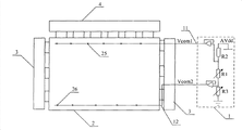
Fig. 4 is the structural representation of common electrode driving circuit the first embodiment of the present invention, and the common electrode driving circuit 1 of present embodiment is used for being connected to liquid crystal panel 2, specifically can be connected in the common electrode layer of the color membrane substrates in the liquid crystal panel 2.Usually transverse and longitudinal is laid with data line and gate line across on the array base palte of this liquid crystal panel 2, the data image signal of data driver 4 outputs is from the side input of data line, an end that is the data line input data signal can be described as data-signal input top, and it is terminal that the other end of data line then is called the data-signal input; The grid line switching signal of gate drivers 3 outputs is from the side input of gate line, i.e. an end of gate line input gate switch signal can be described as gate switch signal input top, and it is terminal that the other end then is called the input of gate switch signal.In liquid crystal panel 2, color membrane substrates and array base palte are to the box setting, and the surface of common electrode layer and array base palte is almost parallel.
As shown in Figure 4, this common electrode driving circuit 1 comprises the first output terminal 11 and the second output terminal 12, and this first output terminal 11 and the second output terminal 12 are respectively applied to export the first common electric voltage Vcom1 and the second common electric voltage Vcom2, and Vcom2 is less than Vcom1.Wherein, the first output terminal 11 is used for being connected to the first end 15 at common electrode layer proximity data signal input top, and apply the first common electric voltage Vcom1 to first end 15, this first end 15 can be point or a plurality of point or the zone at common electrode layer proximity data signal input top, and the first common electric voltage Vcom1 can be applied on these points or the zone by lead-in wire or other modes; The second output terminal 12 is used for being connected to the second terminal end 16 of common electrode layer proximity data signal input, and apply the second common electric voltage Vcom2 to the second end 16, this second end 16 is similar with first end 15, also can be terminal point of common electrode layer proximity data signal input or a plurality of point or zone, the second common electric voltage Vcom2 can be applied on these points or the zone by lead-in wire or other modes.
Because on the array base palte of liquid crystal panel 2, along data line, terminal to the data-signal input from data-signal input top, the suffered lower jumping voltage Δ V of pixel electrode voltage increases gradually, so that pixel electrode voltage reduces gradually; And Vcom2 is terminal to the data-signal input from data-signal input top namely equally along data line less than Vcom1, and the common electric voltage that is applied on the common electrode layer reduces gradually.The variation tendency of pixel electrode voltage and common electric voltage is consistent, by adjusting the difference between Vcom1 and the Vcom2, can be so that pixel electrode voltage be as far as possible consistent with common electric voltage difference between the two, thus improve the scintillation of LCD picture.
The present embodiment common electrode driving circuit is according to the otherness of lower jumping voltage each point on liquid crystal panel, produce respectively different common electric voltages and be applied to different parts on the liquid crystal panel, so that the adjustment amount of common electric voltage is consistent with the lower jumping voltage of each point on the liquid crystal panel as far as possible, improved preferably the whole display effect of whole picture.
Fig. 5 is the structural representation of common electrode driving circuit the second embodiment of the present invention, as shown in Figure 5, in the common electrode driving circuit 1 in the present embodiment, it is that supply voltage AVdd and the second current potential output terminal are between the earth point that the first resistance R 1 is connected to the first current potential output terminal, in actual the enforcement, the first current potential output terminal and the second current potential output terminal also can be for other have the voltage output end of setting potential value, as long as guarantee that the current potential of the first current potential output terminal is greater than the current potential of the second current potential output terminal.The first output terminal 11 is drawn between the first resistance R 1 and supply voltage AVdd, is used for output the first common electric voltage Vcom1; The second output terminal 12 is drawn between the first resistance R 1 and earth point, is used for output the second common electric voltage Vcom2.
On this basis, between the first output terminal 11 and supply voltage AVdd, can also increase by the second resistance R 2, the first resistance R 1 is adjustable resistance, by regulating the size of the first resistance R 1, just can regulate the size of the first common electric voltage Vcom1 of the first output terminal 11 outputs; Between the second output terminal 12 and earth point, can also increase by the 3rd resistance R 3, the 3rd resistance R 3 also can be adjustable resistance, by regulating the size of the first resistance R 1 and/or the 3rd resistance R 3, just can regulate the size of the second common electric voltage Vcom2 of the second output terminal 12 outputs.Wherein, the first resistance R 1, the second resistance R 2 and the 3rd resistance R 3 as long as have at least one to be adjustable resistance, just can reach the function of regulating the first common electric voltage Vcom1 and the second common electric voltage Vcom2.More stable for the voltage that makes output, the first common electric voltage Vcom1 and the second common electric voltage Vcom2 can be respectively through exporting from the first output terminal 11 and the second output terminal 12 behind the operational amplifier again; At this moment, stable through the first common electric voltage Vcom1 and the second common electric voltage Vcom2 magnitude of voltage of the output of operational amplifier amplifier, the internal resistance of common electrode layer can be ignored the impact of the first common electric voltage Vcom1 and the second common electric voltage Vcom2.
Common electrode driving circuit 1 in the present embodiment can be applied to liquid crystal display, preferably is applied to the liquid crystal display of grid bilateral drive form.As shown in Figure 5, first end in the present embodiment can be a plurality of points that are dispersed in common electrode layer proximity data signal input top, can be referred to as the first common electric voltage input end 25 at this, the second end can be to be dispersed in the terminal a plurality of points of common electrode layer proximity data signal input, can be referred to as the second common electric voltage input end 26 at this.The first output terminal 11 is connected to the first common electric voltage input end 25 at common electrode layer proximity data signal input top, and applies the first common electric voltage Vcom1 to this first common electric voltage input end 25; The quantity of this first common electric voltage input end 25 is a plurality of, is distributed in common electrode layer proximity data signal input top.During implementation, can the first output terminal 11 be connected to these the first common electric voltage input ends 25 by a plurality of leads, and apply the first common electric voltage Vcom1 to this first common electric voltage input end 25; Also can adopt in the position at common electrode layer proximity data signal input top, bury the resistivity conductive strips lower than common electrode layer underground, the first output terminal 11 is connected to this conductive strips, and apply the first common electric voltage Vcom1 to it.The second output terminal 12 is connected to the second terminal common electric voltage input end 26 of common electrode layer proximity data signal input, and applies the second common electric voltage Vcom2 to this second common electric voltage input end 26; The quantity of this second common electric voltage input end 26 also is a plurality of, is distributed in the terminal side of common electrode layer proximity data signal input.The embodiment that applies the second common electric voltage Vcom2 to this second common electric voltage input end 26 can be with the mode that applies of the first above-mentioned common electric voltage Vcom1.
For the liquid crystal display of grid bilateral drive form, be provided with two gate drivers 3 in this liquid crystal display, be separately positioned on the both sides of gate line; Each gate line is connected on two gate drivers 3 simultaneously, be subjected to simultaneously the driving of both sides gate drivers 3, in this case, the difference of the lower jumping voltage Δ V that pixel electrode voltage on the liquid crystal panel that the capacitance-resistance characteristic of gate line causes is suffered can be ignored, only consider data line the capacitance-resistance characteristic impact of lower jumping voltage Δ V is got final product, therefore just can adopt the mode of two step voltages input, the first common electric voltage input end 25 and terminal the second common electric voltage input end 26 input the first common electric voltage Vcom1 and the second common electric voltage Vcom2 of proximity data signal input from common electrode layer proximity data signal input top gets final product respectively.As previously mentioned, the quantity of the first common electric voltage input end 25 is a plurality of, be distributed in common electrode layer proximity data signal input top, the quantity of the second common electric voltage input end 26 also is a plurality of, be distributed in the terminal side of common electrode layer proximity data signal input, and the second common electric voltage Vcom2 is less than the first common electric voltage Vcom1.Input different common electric voltages by the upper and lower to the liquid crystal panel common electrode layer like this, and the variation tendency of common electric voltage and pixel electrode voltage is consistent, can improve preferably the scintillation of LCD picture.
The present embodiment common electrode driving circuit is according to the otherness of lower jumping voltage each point on liquid crystal panel, top and bottom to liquid crystal panel apply different common electric voltages respectively, so that the adjustment amount of common electric voltage is consistent with the lower jumping voltage of each point on the liquid crystal panel as far as possible, improved preferably the whole display effect of picture.
Fig. 6 is the structural representation of common electrode driving circuit the 3rd embodiment of the present invention, the common electrode driving circuit 1 of present embodiment is with the key distinction of above-mentioned the second embodiment, but when the equal timing of the first common electric voltage Vcom1 and the second common electric voltage Vcom2, any one of regulating among the two all can affect another size among the second embodiment; And the first common electric voltage Vcom1 in the present embodiment and the second common electric voltage Vcom2 can not affect the size of Vcom1 when regulating Vcom2.
As shown in Figure 6, in the common electrode driving circuit 1 in the present embodiment, it is that supply voltage AVdd and the second current potential output terminal are between the earth point that the first resistance R 1 and the second resistance R 2 are connected in series in the first current potential output terminal, and the first resistance R 1 is adjustable resistance.The first output terminal 11 is drawn between the first resistance R 1 and the second resistance R 2, by regulating the first resistance R 1, just can regulate from the size of the first common electric voltage Vcom1 of the first output terminal 11 outputs.In the implementation, also the second resistance R 2 can be set to adjustable resistance, as long as at least one adjustable, as just can to regulate the first common electric voltage Vcom1 size in the first resistance R 1 and the second resistance R 2.If homogeneity of product is better, the first resistance R 1 and the second resistance R 2 all can be set to fixed resistance.In addition, this common electrode driving circuit 1 comprises that also an end of the 4th resistance R 4, the four resistance R 4 is connected with the second common electric voltage input end 26 on the common electrode layer, and another termination second current potential output terminal is earth point; The amplifier that the second common electric voltage Vcom2 of the second output terminal 12 outputs does not pass through operational amplifier, because common electrode layer is to have certain internal resistance, at this moment, the internal resistance that just is equivalent to this common electrode layer is earth point between connect dividing potential drop at the first output terminal 11 with the second current potential output terminal with the 4th resistance R 4; The first common electric voltage Vcom1 of the first output terminal 11 outputs is higher than the second common electric voltage Vcom2 of the second output terminal 12 outputs.The 4th resistance R 4 is adjustable resistance, by regulating the 4th resistance R 4, the size that just can regulate the second common electric voltage Vcom2; And can not affect the output valve of the first common electric voltage Vcom1 when regulating the second common electric voltage Vcom2.If the second common electric voltage Vcom2 does not need to regulate, also the 4th resistance R 4 can be set to fixed resistance, can also save cost.In order to obtain more stable driving voltage, the first common electric voltage Vcom1 can be from 11 outputs of the first output terminal through operational amplifier.
Present embodiment common electrode driving circuit 1 also can be applied to liquid crystal display as described in the second embodiment, preferably is applied to the liquid crystal display of grid bilateral drive form.Concrete application mode and principle can be described referring to the second embodiment, do not repeat them here.
The present embodiment common electrode driving circuit is according to the otherness of lower jumping voltage each point on liquid crystal panel, top and bottom to liquid crystal panel apply different common electric voltages respectively, so that the adjustment amount of common electric voltage is consistent with the lower jumping voltage of each point on the liquid crystal panel as far as possible, and the adjusting of different common voltage is more convenient, has improved well the whole display effect of picture.
Fig. 7 is the structural representation of common electrode driving circuit the 4th embodiment of the present invention, the key distinction of present embodiment and above-described embodiment is, common electrode driving circuit 1 among above-mentioned the second embodiment and the 3rd embodiment is to be preferably applied to the liquid crystal display that the grid bilateral drives, and the common electrode driving circuit 1 in the present embodiment is the liquid crystal display that is preferably applied to the one-sided driving of grid, but the liquid crystal display of the one-sided driving of this grid can obtain the effect that the grid bilateral drives after designing through inner structure, therefore also can adopt the structure of common electrode driving circuit same with the above-mentioned embodiment 1.The liquid crystal display of certainly, general one-sided drive form also can adopt the common electrode driving circuit 1 of above-described embodiment.
As shown in Figure 7, what the common electrode driving circuit 1 in the present embodiment adopted is the structure of the common electrode driving circuit 1 described in the 3rd embodiment, also can adopt other structures described in above-described embodiment.Structure about concrete common electrode driving circuit 1 can referring to described in the 3rd embodiment, not repeat them here.How the liquid crystal display of the one-sided driving of this grid of following article obtains the effect that the grid bilateral drives.
Be provided with a gate drivers 3 in this liquid crystal display, be arranged on a side of gate line and link to each other with each gate line.Also be provided with gate-on voltage input line 17 and grid is closed voltage input line 18 at the opposite side of gate line, connect each gate line by switch respectively, switch can be thin film transistor (TFT) in the present embodiment.Gate-on voltage input line 17 is connected with gate-on voltage generator 20, inputs gate-on voltages by gate-on voltage generator 20 to gate-on voltage input line 17; Grid is closed voltage input line 18 and is connected with grid and closes voltage generator 21, closes voltage generator 21 by grid and closes voltage input line 18 input grids to grid and close voltage.Wherein, gate-on voltage input line 17 and grid are closed voltage input line 18 and can be arranged on the array base palte; Gate-on voltage generator 20 and grid are closed voltage generator 21 and can be arranged on the data driver 4, the gate-on voltage of its output and grid are closed voltage and are produced by the circuit on the printed circuit board (PCB) that forms data driver 4 (PCB), then are connected on the array base palte by the lead-in wire on the drive IC flexible PCB (COF).Right-hand member at array base palte is provided with the first film transistor 5 and the second thin film transistor (TFT) 6.Wherein, the grid of the first film transistor 5 connects N bar gate line with being connected, and source electrode connects gate-on voltage input line 17; The grid of the second thin film transistor (TFT) 6 connects N+1 bar gate line, and drain electrode connects N bar gate line, and source electrode connects grid and closes voltage input line 18.
This design is so that one-sided driving can obtain the effect that bilateral drives.Concrete principle is as follows: when the conducting of N bar gate line, when gate drivers 3 is inputted gate-on voltage from an end of N bar gate line, the gate turn-on of the first film transistor 5, open gate-on voltage input line 17, input simultaneously gate-on voltage from the other end of this N bar gate line, apply same gate-on voltage at the two ends of N bar gate line simultaneously with regard to being equivalent to like this.In like manner, when N bar gate line is closed and the conducting of N+1 bar gate line, when gate drivers 3 is closed voltage from the end input grid of N bar gate line, the gate turn-on of the second thin film transistor (TFT) 6, open grid and close voltage input line 18, input simultaneously grid from the other end of this N bar gate line and close voltage, close voltage with regard to being equivalent to apply same grid at the two ends of N bar gate line simultaneously like this.Like this, the capacitance-resistance characteristic of N bar gate line just can be ignored on the impact of the lower jumping voltage Δ V of different parts on this grid line, and the capacitance-resistance characteristic of only considering data line gets final product the impact of lower jumping voltage Δ V.In this case, just can adopt the second embodiment and the described common electric voltage of the 3rd embodiment to apply mode, the first common electric voltage input end 25 of inputting top at the common electrode layer proximity data signal of liquid crystal panel is that a plurality of points of upper end and the second common electric voltage input end 26 of proximity data signal input end are a plurality of points of lower end, input respectively different common electric voltages, concrete embodiment can be described referring to the second embodiment and the 3rd embodiment, do not repeat them here.
The present embodiment common electrode driving circuit is according to the otherness of lower jumping voltage each point on panel of LCD, produce respectively different common electric voltages and be applied to different parts on the panel of LCD, so that the adjustment amount of common electric voltage is consistent with the lower jumping voltage of each point on the panel as far as possible, improve preferably the whole display effect of picture, solved the flicker problem of whole picture.
Fig. 8 is the structural representation of common electrode driving circuit the 5th embodiment of the present invention, as shown in Figure 8, common electrode driving circuit 1 in the present embodiment is the structure of common electrode driving circuit 1 among the 4th embodiment that adopts, do not repeat them here, described in above embodiment, also can adopt other versions.
The key distinction of common electrode driving circuit 1 is in present embodiment common electrode driving circuit 1 and above-described embodiment: in the above-described embodiments, the quantity of first end and the second end is a plurality of, and in the present embodiment, the quantity of first end and the second end is one, and first end is proximity data signal input top and the terminal point of crossing setting of gate switch signal input on common electrode layer, can be referred to as the 3rd common electric voltage input end 27 at this; The second end proximity data signal input on common electrode layer point of crossing terminal and gate switch signal input top arranges, and can be referred to as the 4th common electric voltage input end 28 at this.
The common electrode driving circuit 1 of present embodiment can be applied to liquid crystal display, preferably is applicable to the liquid crystal display of the one-sided drive form of grid.Be provided with a gate drivers 3 in the liquid crystal display of this one-sided drive form, this gate drivers 3 is arranged on a side of gate line, and links to each other with each gate line, is used for to each gate line input gate switch signal.Liquid crystal display for this drive form, the first output terminal 11 of common electrode driving circuit 1 is connected to the 3rd common electric voltage input end 27, the second output terminals 12 that common electrode layer proximity data signal input top and the terminal point of crossing of gate switch signal input namely be positioned at the upper right corner and is connected to the terminal and gate switch signal of common electrode layer proximity data signal input and inputs the 4th common electric voltage input end 28 that the point of crossing at top namely is positioned at the lower left corner.The capacitance-resistance characteristic that considers the capacitance-resistance characteristic of gate line and data line on the impact of the lower jumping voltage Δ V of each pixel of liquid crystal panel as can be known, it is maximum to jump voltage Δ V under the lower left corner of liquid crystal panel 2, the lower jumping voltage Δ V in the upper right corner is minimum.At this moment, considering on the basis of data line capacitance-resistance characteristic to lower jumping voltage influence, consider that simultaneously gate line capacitance-resistance characteristic is on the impact of lower jumping voltage, namely so that the common electric voltage of input common electrode layer different common voltage input end along data-signal input top to the data-signal input is terminal reduce gradually in, the common electric voltage of this input also increases gradually along gate switch signal input top to gate switch signal input end
Accordingly, the common electric voltage of present embodiment is taked the mode of aforesaid two step voltages input, the 3rd common electric voltage input end 27 to the common electrode layer upper right corner applies the first common electric voltage Vcom1, the 4th common electric voltage input end 28 to the common electrode layer lower left corner applies the second common electric voltage Vcom2, and Vcom2 is less than Vcom1.Variation tendency from Vcom1 to Vcom2 is consistent with the variation tendency of the pixel electrode voltage of array base palte, and the internal resistance of the common electrode layer dividing potential drop of connecting with R4, by regulating R1 and R4, can regulate the size of Vcom1 and Vcom2, as far as possible so that the difference between Vcom1 and the Vcom2 equals the difference of the lower jumping voltage Δ V2 of the lower jumping voltage Δ V1 of the upper right corner the 3rd common electric voltage input end 27 on the liquid crystal panel and the lower left corner the 4th common electric voltage input end 28, thereby improve preferably the flicker problem of liquid crystal display picture.
In the common electrode driving circuit 1 of present embodiment, in the stable situation of liquid crystal panel 2 products, be the capacitance-resistance characteristic of the gate line of liquid crystal panel 2 and data line when consistent, the 4th resistance R 4 can adopt fixed resistance to save cost, and the size of regulating at ordinary times the first common electric voltage Vcom1 gets final product; In the unsettled situation of liquid crystal panel 2 products, the capacitance-resistance characteristic that is the gate line that causes of each opposite sex of liquid crystal panel 2 and data line is inconsistent, and so that the lower jumping voltage Δ V of each liquid crystal panel 2 when inconsistent, the 4th resistance R 4 can be set to adjustable resistance, by regulating the size of R4, just can be adjusted in the size of the second common electric voltage Vcom2 in the lower left corner, the variation of lower jumping voltage Δ V on itself and the liquid crystal panel 2 is approached, thereby obtain good display effect, in actual experiment, can obtain approximately the effect of improving of 2db.In addition, the first common electric voltage Vcom1 also can export through behind the operational amplifier, like this can be so that the voltage of output is more stable.
The present embodiment common electrode driving circuit is according to the otherness of lower jumping voltage each point on liquid crystal panel, the upper right corner to liquid crystal panel applies different two-stage common electric voltages with the lower left corner respectively, so that the adjustment amount of common electric voltage is consistent with the lower jumping voltage of each point on the liquid crystal panel as far as possible, improved preferably the whole display effect of picture.
Fig. 9 is the structural representation of common electrode driving circuit the 6th embodiment of the present invention, as shown in Figure 9, the common electrode driving circuit 1 of present embodiment has increased again two common electric voltage output terminals on the basis of the 5th embodiment, concrete, also comprise the 3rd output terminal 13 and the 4th output terminal 14.Wherein, the 3rd output terminal 13 be used for being connected to common electrode layer proximity data signal input top and gate switch signal input top the 5th common electric voltage input end 29 of point of crossing, and apply the 3rd common electric voltage Vcom3 to the 5th common electric voltage input end 29, the 4th output terminal 14 is used for being connected to common electrode layer proximity data signal and inputs the 6th common electric voltage the input end 30 terminal and point of crossing that the input of gate switch signal is terminal, and apply the 4th common electric voltage Vcom4 to the 6th common electric voltage input end 30, and the value of the 3rd common electric voltage Vcom3 and the 4th common electric voltage Vcom4 is between the first common electric voltage Vcom1 and the second common electric voltage Vcom2, respectively greater than the second common electric voltage Vcom2, and respectively less than described the first common electric voltage Vcom1, and the 3rd common electric voltage Vcom3 is less than the 4th common electric voltage Vcom4.
The common electrode driving circuit 1 of present embodiment is also on the basis of the 5th embodiment, increasing by three resistance in seriess the 5th resistance R 5, the 6th resistance R 6 and the 7th resistance R 7, the five resistance R 5, the 6th resistance R 6 and the 7th resistance R 7 dividing potential drop of between the first output terminal 11 and the second output terminal 12, connecting between the first output terminal 11 and the second output terminal 12.The 3rd output terminal 13 is drawn between the 5th resistance R 5 and the 6th resistance R 6, be used for being connected to the 5th common electric voltage input end 29 in liquid crystal panel 2 upper left corners and applying the 3rd common electric voltage Vcom3, the 4th output terminal 14 is drawn between the 6th resistance R 6 and the 7th resistance R 7, be used for being connected to the 6th common electric voltage input end 30 in liquid crystal panel 2 lower right corner, and apply the 4th common electric voltage Vcom4 to the 6th common electric voltage input end 30, and the 3rd common electric voltage Vcom3 is less than the 4th common electric voltage Vcom4.
Similar with other embodiment, in the common electrode driving circuit 1 of present embodiment, the first resistance R 1 also can not be connected between supply voltage AVdd and the earth point, but be connected between other the first current potential output terminals and the second current potential output terminal, as long as guarantee that the current potential of the first current potential output terminal is greater than the current potential of the second current potential output terminal.In the first resistance R 1 and the second resistance R 2 any one is set to adjustable resistance or two and all is set to adjustable resistance, all can regulate the size of the first common electric voltage Vcom1.In the stable situation of liquid crystal panel 2 products, the 4th resistance R 4 can be set to fixed resistance; Also the 4th resistance R 4 can be set to adjustable resistance, just can regulate the size of the second common electric voltage Vcom2 by regulating the 4th resistance R 4.In the 5th resistance R 5, the 6th resistance R 6 and the 7th resistance R 7, as long as at least one resistance is adjustable resistance, just can regulate the size of the 3rd common electric voltage Vcom3 and the 4th common electric voltage Vcom4 equally.In order to obtain comparatively stable voltage, the first common electric voltage Vcom1, the second common electric voltage Vcom2, the 3rd common electric voltage Vcom3 and the 4th common electric voltage Vcom4 all can export through after the amplifier of operational amplifier.
The common electrode driving circuit 1 of present embodiment can be applied to liquid crystal display, preferably is applied to the liquid crystal display of the one-sided drive form of grid.Liquid crystal display for the one-sided drive form of grid, because according to the impact analysis to lower jumping voltage Δ V of comprehensive gate line capacitance-resistance characteristic and data line capacitance-resistance characteristic, lower jumping voltage Δ V is maximum in the lower left corner of liquid crystal panel 2, takes second place in the upper left corner, take second place again in the lower right corner, the upper right corner is minimum.Accordingly, adopt above-mentioned level Four voltage input mode, namely apply the first common electric voltage Vcom1 in the upper right corner of liquid crystal panel 2, the lower left corner applies on the basis of the second common electric voltage Vcom2, apply again the 3rd common electric voltage Vcom3 and the lower right corner in the upper left corner and apply the 4th common electric voltage Vcom4, and Vcom3 is less than Vcom4, by this way, can be so that the display effect of LCD picture be more desirable.
The present embodiment common electrode driving circuit is according to the otherness of lower jumping voltage each point on liquid crystal panel, the upper right corner, the lower left corner, the upper left corner and the lower right corner to liquid crystal panel applies different level Four common electric voltages respectively, so that the adjustment amount of common electric voltage is consistent with the lower jumping voltage of each point on the liquid crystal panel as far as possible, improved preferably the whole display effect of picture.
Figure 10 is the structural representation of common electrode driving circuit the 7th embodiment of the present invention, as shown in figure 10, common electrode driving circuit 1 in the present embodiment also is to have four output terminals, i.e. the first output terminal 11, the second output terminal 12, the 3rd output terminal 13 and the 4th output terminal 14, and the purposes of these four output terminals is described also identical with the 6th embodiment.Different is that the structure of the common electrode driving circuit 1 of the common electric voltage of exporting for generation of these four output terminals in the present embodiment is different.
The common electrode driving circuit 1 of present embodiment is on the basis of the structure of the common electrode driving circuit 1 of the second embodiment, between the first output terminal 11 and the second output terminal 12, increase again the resistance of three series connection, be respectively the 4th resistance R 4, the 5th resistance R 5 and the 6th resistance R 6.The 3rd output terminal 13 is drawn between the 4th resistance R 4 and the 5th resistance R 5, and the 4th output terminal 14 is drawn between the 5th resistance R 5 and the 6th resistance R 6.Can change by the resistance value of regulating the first resistance R 1 and the 3rd resistance R 3 size of the first common electric voltage Vcom1 and the second common electric voltage Vcom2.And the first common electric voltage Vcom1 and the second common electric voltage Vcom2 can drive by an operational amplifier, thereby can guarantee better the stability of this voltage.The 4th resistance R 4, the 5th resistance R 5 and the 6th resistance R 6 are fixed resistance, and wherein at least one also can be adjustable resistance, just can change the size of the 3rd common electric voltage Vcom3 and the 4th common electric voltage Vcom4 by the resistance of regulating adjustable resistance.
Present embodiment common electrode driving circuit 1 is according to the otherness of lower jumping voltage each point on liquid crystal panel 2, four summits on the liquid crystal panel 2 apply different common electric voltages respectively, so that the adjustment amount of common electric voltage is consistent with the lower jumping voltage of each point on the liquid crystal panel 2 as far as possible, improved preferably the whole display effect of picture.
The present invention also provides the liquid crystal display that adopts the described common electrode driving circuit structure of above embodiment, the common electrode driving circuit of this liquid crystal display links to each other with common electrode layer, is used for the different common voltage input end input common electric voltage to common electrode layer.Among following the embodiment for liquid crystal display, the common electrode layer of liquid crystal display is arranged on the color membrane substrates.
Figure 11 is the structural representation of liquid crystal display the first embodiment of the present invention, as shown in figure 11, the liquid crystal display of present embodiment is the liquid crystal display of the one-sided drives structure of grid, it comprises common electrode driving circuit 1, liquid crystal panel, gate drivers 3 and data driver 4, wherein, liquid crystal panel is formed by array base palte 22 and 23 pairs of boxes of color membrane substrates, is filled with liquid crystal layer 24 therebetween; And array base palte 22 comprises transverse and longitudinal intersects to form on first substrate and the described first substrate a plurality of gate lines and data line; Color membrane substrates 23 comprises the common electrode layer 19 that forms on second substrate and the second substrate; The quantity of the gate drivers 3 of liquid crystal display is one, and a side that is arranged on gate line links to each other with each gate line, is used for to gate line input gate switch signal; Data driver 4 is used for to the data line outputting data signals, and common electrode driving circuit 1 is arranged on the data driver 4, and common electrode driving circuit 1 links to each other with common electrode layer 19 on the color membrane substrates 23, for applying common electric voltage to common electrode layer 19.
Common electrode driving circuit 1 in the present embodiment can adopt the described arbitrary structure of aforesaid common electrode driving circuit the first embodiment to the seven embodiment, and concrete structure and application see aforesaid each embodiment for details, do not repeat them here.
Figure 12 is the structural representation of liquid crystal display the second embodiment of the present invention, as shown in figure 12, the key distinction of present embodiment and the first embodiment is, liquid crystal display in the present embodiment is the liquid crystal display of grid bilateral drives structure, the quantity of gate drivers 3 is two, divides the both sides that are located at gate line; Each gate line is connected on two gate drivers 3 simultaneously, is subjected to simultaneously the driving of both sides gate drivers 3.
Common electrode driving circuit 1 in the present embodiment can adopt the described structure of aforesaid the first embodiment to the three embodiment, be the liquid crystal display in the present embodiment owing to be the structure that the grid bilateral drives, the gate line characteristic can be ignored the impact of lower jumping voltage, just can only consider the data line characteristic to the impact of lower jumping voltage this moment, respectively to data-signal input top and data-signal input terminal input the first common electric voltage and the second common electric voltage.Concrete structure and application see aforesaid each embodiment for details, do not repeat them here.
Figure 13 is the structural representation of liquid crystal display the 3rd embodiment of the present invention, as shown in figure 13, present embodiment is identical with the second embodiment, also be to have the effect that bilateral drives, common electrode driving circuit 1 also can adopt the described structure of aforesaid the first embodiment to the three embodiment, only consider the data line characteristic to the impact of lower jumping voltage, respectively to data-signal input top and data-signal input terminal input the first common electric voltage and the second common electric voltage.
But the key distinction of itself and the second embodiment is that the effect that the bilateral of present embodiment liquid crystal display drives is not because it has two gate drivers, but the one-sided driving of grid but drive effect through having bilateral after the architecture advances.Its concrete structure is, the quantity of gate drivers 3 is one, and a side that is arranged on gate line links to each other with each gate line; Also be provided with the gate-on voltage input line and grid is closed voltage input line at the opposite side of gate line, connect each gate line by switch respectively; When an end of gate line is inputted gate-on voltage, open the gate-on voltage input line at gate drivers 3, input simultaneously gate-on voltage from the other end of this gate line; When the end input grid of gate line is closed voltage, open grid at gate drivers 3 and close voltage input line, input simultaneously grid from the other end of this gate line and close voltage.Concrete structure and principle can see for details described in common electrode driving circuit the 4th embodiment of the present invention, do not repeat them here.
Above embodiment liquid crystal display is according to the otherness of lower jumping voltage each point on panel of LCD, different parts on the panel applies different common electric voltages respectively, so that the adjustment amount of common electric voltage is consistent with the lower jumping voltage of each point on the panel as far as possible, improved preferably the whole display effect of picture, solved the flicker problem of whole picture, but also use adjustable resistance to be convenient to regulate the common electric voltage value, drive so that common electric voltage output is more stable with operational amplifier.
It should be noted that at last: above embodiment is only in order to technical scheme of the present invention to be described but not limit it, although with reference to preferred embodiment the present invention is had been described in detail, those of ordinary skill in the art is to be understood that: it still can be made amendment or be equal to replacement technical scheme of the present invention, and these modifications or be equal to replacement and also can not make amended technical scheme break away from the spirit and scope of technical solution of the present invention.
Claims (4)
1. a common electrode driving circuit is used for multistage grid and drives liquid crystal display, it is characterized in that,
Comprise:
A plurality of output terminals, described a plurality of output terminals are used for being connected to a plurality of common electric voltage input ends of common electrode layer, and to described a plurality of common electric voltage input end input common electric voltages;
Described a plurality of common electric voltages of input are inputted end along data-signal input top to data-signal and are reduced gradually;
Described a plurality of output terminal comprises:
The first output terminal is used for being connected to the 3rd common electric voltage input end that common electrode layer proximity data signal is inputted the point of crossing of top and gate switch signal input end, and applies the first common electric voltage to described the 3rd common electric voltage input end;
The second output terminal, be used for being connected to the 4th common electric voltage input end that common electrode layer proximity data signal is inputted the point of crossing at terminal and gate switch signal input top, and apply the second common electric voltage to described the 4th common electric voltage input end, and described the second common electric voltage is less than described the first common electric voltage;
The 3rd output terminal is used for being connected to the 5th common electric voltage input end that common electrode layer proximity data signal is inputted the point of crossing at top and gate switch signal input top, and applies the 3rd common electric voltage to described the 5th common electric voltage input end;
The 4th output terminal is used for being connected to common electrode layer proximity data signal and inputs the 6th common electric voltage the input end terminal and point of crossing that the input of gate switch signal is terminal, and applies the 4th common electric voltage to described the 6th common electric voltage input end;
Described the 3rd common electric voltage and the 4th common electric voltage be respectively greater than described the second common electric voltage, and respectively less than described the first common electric voltage, and described the 3rd common electric voltage is less than described the 4th common electric voltage.
2. common electrode driving circuit according to claim 1 is characterized in that, described a plurality of common electric voltages of input are also inputted end along gate switch signal input top to the gate switch signal and increased gradually.
3. common electrode driving circuit according to claim 1, it is characterized in that, before described the 3rd common electric voltage input end, the 4th common electric voltage input end, the 5th common electric voltage input end and/or the 6th common electric voltage input end, also be connected with operational amplifier.
4. a liquid crystal display that comprises the arbitrary described common electrode driving circuit of claim 1~3 is characterized in that, described liquid crystal display comprises liquid crystal panel, and described liquid crystal panel is formed box by array base palte and color membrane substrates, is filled with liquid crystal layer therebetween; And described array base palte comprises transverse and longitudinal intersects to form on first substrate and the described first substrate a plurality of gate lines and data line; Described liquid crystal display also comprises gate drivers and data driver, and described gate drivers is used for to described gate line output gate switch signal, and described data driver is used for to described data line outputting data signals; The quantity of described gate drivers is one, and a side that is arranged on described gate line links to each other with each gate line, is used for input gate switch signal; Described common electrode driving circuit links to each other with common electrode layer in the described liquid crystal display.
Priority Applications (5)
| Application Number | Priority Date | Filing Date | Title |
|---|---|---|---|
| CN2009100807005A CN101847376B (en) | 2009-03-25 | 2009-03-25 | Common electrode driving circuit and LCD |
| US12/730,373 US8878829B2 (en) | 2009-03-25 | 2010-03-24 | Liquid crystal display and common electrode drive circuit thereof |
| JP2010070127A JP5727153B2 (en) | 2009-03-25 | 2010-03-25 | Common electrode drive circuit and liquid crystal display |
| KR1020100026697A KR101154491B1 (en) | 2009-03-25 | 2010-03-25 | Common electrode driving circuit and liquid crystal display |
| KR1020120016058A KR101233710B1 (en) | 2009-03-25 | 2012-02-16 | Common electrode driving circuit and liquid crystal display |
Applications Claiming Priority (1)
| Application Number | Priority Date | Filing Date | Title |
|---|---|---|---|
| CN2009100807005A CN101847376B (en) | 2009-03-25 | 2009-03-25 | Common electrode driving circuit and LCD |
Publications (2)
| Publication Number | Publication Date |
|---|---|
| CN101847376A CN101847376A (en) | 2010-09-29 |
| CN101847376B true CN101847376B (en) | 2013-10-30 |
Family
ID=42771975
Family Applications (1)
| Application Number | Title | Priority Date | Filing Date |
|---|---|---|---|
| CN2009100807005A Active CN101847376B (en) | 2009-03-25 | 2009-03-25 | Common electrode driving circuit and LCD |
Country Status (4)
| Country | Link |
|---|---|
| US (1) | US8878829B2 (en) |
| JP (1) | JP5727153B2 (en) |
| KR (2) | KR101154491B1 (en) |
| CN (1) | CN101847376B (en) |
Families Citing this family (32)
| Publication number | Priority date | Publication date | Assignee | Title |
|---|---|---|---|---|
| TWM395186U (en) * | 2010-06-15 | 2010-12-21 | Chunghwa Picture Tubes Ltd | Display apparatus and display panel thereof |
| JP5670693B2 (en) | 2010-10-14 | 2015-02-18 | 矢崎総業株式会社 | Battery voltage monitoring device |
| JP5687487B2 (en) * | 2010-12-28 | 2015-03-18 | 株式会社ジャパンディスプレイ | Driving circuit |
| CN102314010B (en) * | 2011-09-05 | 2014-10-29 | 深圳市华星光电技术有限公司 | Liquid crystal display panel and voltage control method thereof |
| CN103295539B (en) * | 2012-04-24 | 2015-07-22 | 上海天马微电子有限公司 | Liquid crystal display panel |
| CN103295540B (en) | 2012-06-07 | 2015-06-10 | 上海天马微电子有限公司 | Driving method, driving device and display for active matrix display panel |
| US8941640B2 (en) | 2012-06-08 | 2015-01-27 | Apple Inc. | Differential VCOM resistance or capacitance tuning for improved image quality |
| US9064464B2 (en) | 2012-06-25 | 2015-06-23 | Apple Inc. | Systems and methods for calibrating a display to reduce or eliminate mura artifacts |
| CN103258515B (en) * | 2013-05-13 | 2015-08-05 | 京东方科技集团股份有限公司 | Gate drive voltage feeding mechanism, Supply Method and display device |
| CN103345091A (en) * | 2013-07-05 | 2013-10-09 | 深圳市华星光电技术有限公司 | Display panel, driving method thereof and display device thereof |
| KR20150116068A (en) | 2014-04-04 | 2015-10-15 | 삼성디스플레이 주식회사 | Display device |
| CN104299593B (en) * | 2014-11-07 | 2017-01-25 | 深圳市华星光电技术有限公司 | Liquid crystal display device |
| CN104537978A (en) * | 2015-01-23 | 2015-04-22 | 京东方科技集团股份有限公司 | Display panel, drive method of display panel, and display device |
| CN104777942B (en) * | 2015-05-08 | 2018-02-06 | 厦门天马微电子有限公司 | Touch-control display panel, driving method and touch control display apparatus |
| TWI534793B (en) | 2015-05-21 | 2016-05-21 | 友達光電股份有限公司 | Liquid crstal display |
| US10380937B2 (en) * | 2015-08-26 | 2019-08-13 | Apple Inc. | Multi-zoned variable VCOM control |
| CN105137675B (en) * | 2015-09-30 | 2018-01-12 | 深圳市华星光电技术有限公司 | A kind of array base palte and liquid crystal display panel |
| US9805677B2 (en) * | 2015-12-28 | 2017-10-31 | Panasonic Liquid Crystal Display Co., Ltd. | Display device for adjusting current output of a common voltage generating circuit |
| CN105895041B (en) | 2016-06-06 | 2018-08-24 | 深圳市华星光电技术有限公司 | common electrode drive module and liquid crystal display panel |
| US10832627B2 (en) * | 2016-07-14 | 2020-11-10 | Novatek Microelectronics Corp. | Display apparatus and source driver thereof and operating method |
| CN106683633B (en) * | 2017-03-20 | 2019-04-30 | 京东方科技集团股份有限公司 | A kind of method of adjustment and device of display module |
| CN107121852B (en) * | 2017-06-20 | 2020-05-05 | 武汉华星光电技术有限公司 | Array substrate and liquid crystal panel |
| CN107591143A (en) * | 2017-10-18 | 2018-01-16 | 京东方科技集团股份有限公司 | Common electric voltage compensating unit, compensation method, drive circuit and display panel |
| CN107665686A (en) * | 2017-10-19 | 2018-02-06 | 京东方科技集团股份有限公司 | A kind of driving method, drive device and display device |
| CN108287420A (en) | 2018-02-08 | 2018-07-17 | 武汉华星光电技术有限公司 | The common electrode and display panel of display panel |
| CN109036255A (en) * | 2018-09-30 | 2018-12-18 | 厦门天马微电子有限公司 | A kind of display driving method, display drive apparatus and display equipment |
| CN109584833B (en) * | 2019-01-21 | 2021-06-01 | 深圳市华星光电半导体显示技术有限公司 | Display panel and display device |
| CN109785811B (en) * | 2019-01-29 | 2021-03-02 | 重庆京东方光电科技有限公司 | Common voltage supply circuit, liquid crystal display panel and driving method thereof |
| JP2020140032A (en) * | 2019-02-27 | 2020-09-03 | セイコーエプソン株式会社 | Voltage supply circuit, liquid crystal device, electronic apparatus and mobile body |
| CN113140191A (en) * | 2021-04-16 | 2021-07-20 | 武汉华星光电技术有限公司 | Display device |
| CN114442344B (en) | 2021-12-31 | 2023-10-24 | 上海中航光电子有限公司 | Visual angle switchable display module and vehicle |
| CN117079617B (en) * | 2023-10-12 | 2024-02-13 | 惠科股份有限公司 | Brightness adjusting method for display panel and display panel |
Citations (2)
| Publication number | Priority date | Publication date | Assignee | Title |
|---|---|---|---|---|
| CN87106311A (en) * | 1986-09-15 | 1988-03-30 | 菲利浦光灯制造公司 | Display device |
| US6229510B1 (en) * | 1997-07-23 | 2001-05-08 | Samsung Electronics Co., Ltd. | Liquid crystal display having different common voltages |
Family Cites Families (18)
| Publication number | Priority date | Publication date | Assignee | Title |
|---|---|---|---|---|
| JP2608403B2 (en) * | 1987-01-17 | 1997-05-07 | 富士通株式会社 | Driving method of active matrix type liquid crystal panel |
| JPH09218388A (en) * | 1996-02-09 | 1997-08-19 | Hosiden Corp | Liquid crystal display device |
| JPH1039325A (en) | 1996-07-26 | 1998-02-13 | Toshiba Corp | Active matrix type liquid crystal display device |
| KR100495801B1 (en) | 1997-07-23 | 2005-09-15 | 삼성전자주식회사 | Liquid crystal display device for compensating kickback voltage and driving method |
| KR100590746B1 (en) * | 1998-11-06 | 2006-10-04 | 삼성전자주식회사 | Liquid crystal display with different common voltages |
| KR100604718B1 (en) * | 1999-07-05 | 2006-07-28 | 엘지.필립스 엘시디 주식회사 | Liquid crystal display device and the method for compensating the kickback voltage therof |
| JP3594131B2 (en) | 2000-07-28 | 2004-11-24 | シャープ株式会社 | Image display device |
| KR100796787B1 (en) | 2001-01-04 | 2008-01-22 | 삼성전자주식회사 | Liquid crystal display system, panel and method for compensating gate line delay |
| KR100482160B1 (en) | 2002-09-04 | 2005-04-13 | 엘지.필립스 엘시디 주식회사 | array substrate of liquid crystal display device |
| JP2004191581A (en) * | 2002-12-10 | 2004-07-08 | Sharp Corp | Liquid crystal display unit and its driving method |
| KR100900548B1 (en) * | 2002-12-17 | 2009-06-02 | 삼성전자주식회사 | Liquid crystal display for generating common voltages with different values |
| KR20050033670A (en) * | 2003-10-07 | 2005-04-13 | 엘지.필립스 엘시디 주식회사 | Lcd and the driving method |
| KR100995639B1 (en) * | 2003-12-30 | 2010-11-19 | 엘지디스플레이 주식회사 | Liquid Crystal Display Device And Driving Method Thereof |
| KR101136318B1 (en) * | 2005-04-29 | 2012-04-19 | 엘지디스플레이 주식회사 | Liquid Crystal Display device |
| KR101167314B1 (en) * | 2005-06-29 | 2012-07-19 | 엘지디스플레이 주식회사 | Liquid Crystal Display device |
| KR101177593B1 (en) * | 2005-12-29 | 2012-08-27 | 엘지디스플레이 주식회사 | Liquid crystal display device |
| JP2007193122A (en) * | 2006-01-19 | 2007-08-02 | Toshiba Matsushita Display Technology Co Ltd | Liquid crystal display device |
| TWI354968B (en) * | 2006-11-17 | 2011-12-21 | Chunghwa Picture Tubes Ltd | Liquid crystal display and display panel thereof |
-
2009
- 2009-03-25 CN CN2009100807005A patent/CN101847376B/en active Active
-
2010
- 2010-03-24 US US12/730,373 patent/US8878829B2/en active Active
- 2010-03-25 JP JP2010070127A patent/JP5727153B2/en active Active
- 2010-03-25 KR KR1020100026697A patent/KR101154491B1/en active IP Right Grant
-
2012
- 2012-02-16 KR KR1020120016058A patent/KR101233710B1/en active IP Right Grant
Patent Citations (2)
| Publication number | Priority date | Publication date | Assignee | Title |
|---|---|---|---|---|
| CN87106311A (en) * | 1986-09-15 | 1988-03-30 | 菲利浦光灯制造公司 | Display device |
| US6229510B1 (en) * | 1997-07-23 | 2001-05-08 | Samsung Electronics Co., Ltd. | Liquid crystal display having different common voltages |
Also Published As
| Publication number | Publication date |
|---|---|
| US8878829B2 (en) | 2014-11-04 |
| US20100245326A1 (en) | 2010-09-30 |
| KR101233710B1 (en) | 2013-02-18 |
| JP5727153B2 (en) | 2015-06-03 |
| KR20100107422A (en) | 2010-10-05 |
| CN101847376A (en) | 2010-09-29 |
| JP2010231205A (en) | 2010-10-14 |
| KR20120031197A (en) | 2012-03-30 |
| KR101154491B1 (en) | 2012-07-03 |
Similar Documents
| Publication | Publication Date | Title |
|---|---|---|
| CN101847376B (en) | Common electrode driving circuit and LCD | |
| US8228274B2 (en) | Liquid crystal panel, liquid crystal display, and driving method thereof | |
| CN101154367B (en) | Display driving apparatus and display apparatus comprising the same | |
| CN101221730B (en) | Liquid crystal display | |
| CN101675374B (en) | Liquid crystal display device | |
| KR101920885B1 (en) | Display device and driving method thereof | |
| US20100033475A1 (en) | Liquid crystal display and control method thereof | |
| US20080252632A1 (en) | Gamma voltage generating circuit and display device having the same | |
| KR100895305B1 (en) | Liquid crystal display and driving method thereof | |
| KR100440360B1 (en) | LCD and its driving method | |
| CN101311781A (en) | LCD device and its public voltage drive method | |
| CN109727587B (en) | Liquid crystal display for improving bright and dark bands caused by backlight frequency change | |
| CN100444236C (en) | Liquid crystal display driving method and driving circuit | |
| CN106971697A (en) | Display device | |
| CN101963728A (en) | Liquid crystal display | |
| CN102763031A (en) | Liquid-crystal display device | |
| KR102023949B1 (en) | Liquid crystal display device and method for driving the same | |
| KR100840317B1 (en) | liquid crystal device for compensating kick-back voltage and driving device thereof | |
| CN109949755B (en) | Feed-through voltage compensation circuit and liquid crystal display device | |
| US20150185531A1 (en) | Liquid crystal display panel, pixel structure and driving method thereof | |
| KR101264704B1 (en) | LCD and drive method thereof | |
| KR20070068098A (en) | Liquid crystal display for reducing kickback noise | |
| CN110850654B (en) | Liquid crystal display panel | |
| KR20070068096A (en) | Liquid crystal display | |
| KR20080046987A (en) | Display apparatus |
Legal Events
| Date | Code | Title | Description |
|---|---|---|---|
| C06 | Publication | ||
| PB01 | Publication | ||
| C10 | Entry into substantive examination | ||
| SE01 | Entry into force of request for substantive examination | ||
| C14 | Grant of patent or utility model | ||
| GR01 | Patent grant |