EP2626801A2 - Configuring a programmable device using high-level language - Google Patents
Configuring a programmable device using high-level language Download PDFInfo
- Publication number
- EP2626801A2 EP2626801A2 EP20130154773 EP13154773A EP2626801A2 EP 2626801 A2 EP2626801 A2 EP 2626801A2 EP 20130154773 EP20130154773 EP 20130154773 EP 13154773 A EP13154773 A EP 13154773A EP 2626801 A2 EP2626801 A2 EP 2626801A2
- Authority
- EP
- European Patent Office
- Prior art keywords
- input
- stall
- data
- compiling
- output
- Prior art date
- Legal status (The legal status is an assumption and is not a legal conclusion. Google has not performed a legal analysis and makes no representation as to the accuracy of the status listed.)
- Granted
Links
Images





Classifications
-
- G—PHYSICS
- G06—COMPUTING OR CALCULATING; COUNTING
- G06F—ELECTRIC DIGITAL DATA PROCESSING
- G06F30/00—Computer-aided design [CAD]
- G06F30/30—Circuit design
- G06F30/34—Circuit design for reconfigurable circuits, e.g. field programmable gate arrays [FPGA] or programmable logic devices [PLD]
- G06F30/347—Physical level, e.g. placement or routing
-
- G—PHYSICS
- G06—COMPUTING OR CALCULATING; COUNTING
- G06F—ELECTRIC DIGITAL DATA PROCESSING
- G06F30/00—Computer-aided design [CAD]
- G06F30/30—Circuit design
- G06F30/32—Circuit design at the digital level
- G06F30/327—Logic synthesis; Behaviour synthesis, e.g. mapping logic, HDL to netlist, high-level language to RTL or netlist
-
- G—PHYSICS
- G06—COMPUTING OR CALCULATING; COUNTING
- G06F—ELECTRIC DIGITAL DATA PROCESSING
- G06F30/00—Computer-aided design [CAD]
- G06F30/30—Circuit design
- G06F30/34—Circuit design for reconfigurable circuits, e.g. field programmable gate arrays [FPGA] or programmable logic devices [PLD]
-
- G—PHYSICS
- G06—COMPUTING OR CALCULATING; COUNTING
- G06F—ELECTRIC DIGITAL DATA PROCESSING
- G06F30/00—Computer-aided design [CAD]
- G06F30/30—Circuit design
- G06F30/39—Circuit design at the physical level
- G06F30/394—Routing
-
- G—PHYSICS
- G06—COMPUTING OR CALCULATING; COUNTING
- G06F—ELECTRIC DIGITAL DATA PROCESSING
- G06F30/00—Computer-aided design [CAD]
- G06F30/30—Circuit design
- G06F30/39—Circuit design at the physical level
- G06F30/398—Design verification or optimisation, e.g. using design rule check [DRC], layout versus schematics [LVS] or finite element methods [FEM]
-
- H—ELECTRICITY
- H03—ELECTRONIC CIRCUITRY
- H03K—PULSE TECHNIQUE
- H03K19/00—Logic circuits, i.e. having at least two inputs acting on one output; Inverting circuits
- H03K19/02—Logic circuits, i.e. having at least two inputs acting on one output; Inverting circuits using specified components
- H03K19/173—Logic circuits, i.e. having at least two inputs acting on one output; Inverting circuits using specified components using elementary logic circuits as components
- H03K19/177—Logic circuits, i.e. having at least two inputs acting on one output; Inverting circuits using specified components using elementary logic circuits as components arranged in matrix form
- H03K19/17736—Structural details of routing resources
-
- H—ELECTRICITY
- H04—ELECTRIC COMMUNICATION TECHNIQUE
- H04L—TRANSMISSION OF DIGITAL INFORMATION, e.g. TELEGRAPHIC COMMUNICATION
- H04L41/00—Arrangements for maintenance, administration or management of data switching networks, e.g. of packet switching networks
- H04L41/08—Configuration management of networks or network elements
- H04L41/0803—Configuration setting
- H04L41/0806—Configuration setting for initial configuration or provisioning, e.g. plug-and-play
-
- H—ELECTRICITY
- H04—ELECTRIC COMMUNICATION TECHNIQUE
- H04L—TRANSMISSION OF DIGITAL INFORMATION, e.g. TELEGRAPHIC COMMUNICATION
- H04L49/00—Packet switching elements
- H04L49/35—Switches specially adapted for specific applications
-
- G—PHYSICS
- G06—COMPUTING OR CALCULATING; COUNTING
- G06F—ELECTRIC DIGITAL DATA PROCESSING
- G06F2115/00—Details relating to the type of the circuit
- G06F2115/08—Intellectual property [IP] blocks or IP cores
-
- G—PHYSICS
- G06—COMPUTING OR CALCULATING; COUNTING
- G06F—ELECTRIC DIGITAL DATA PROCESSING
- G06F2119/00—Details relating to the type or aim of the analysis or the optimisation
- G06F2119/06—Power analysis or power optimisation
-
- G—PHYSICS
- G06—COMPUTING OR CALCULATING; COUNTING
- G06F—ELECTRIC DIGITAL DATA PROCESSING
- G06F30/00—Computer-aided design [CAD]
- G06F30/30—Circuit design
- G06F30/39—Circuit design at the physical level
Definitions
- This invention relates to the use of a high-level language to configure a programmable integrated circuit devices such as a field-programmable gate array (FPGAs) or other type of programmable logic devices (PLDs).
- FPGAs field-programmable gate array
- PLDs programmable logic devices
- programmable devices were one-time configurable. For example, configuration may have been achieved by "blowing” - i.e., opening - fusible links. Alternatively, the configuration may have been stored in a programmable read-only memory. Those devices generally provided the user with the ability to configure the devices for "sum-of-products" (or "P-TERM”) logic operations. Later, such programmable logic devices incorporating erasable programmable read-only memory (EPROM) for configuration became available, allowing the devices to be reconfigured.
- PROM erasable programmable read-only memory
- SRAM static random access memory
- Such devices began to be provided with embedded blocks of random access memory that could be configured by the user to act as random access memory, read-only memory, or logic (such as P-TERM logic).
- logic such as P-TERM logic
- dedicated circuits could include phase-locked loops or delay-locked loops for clock generation, as well as various circuits for various mathematical operations such as addition or multiplication. This spares users from having to create equivalent circuits by configuring the available general-purpose programmable logic.
- Such software also now commonly includes pre-defined functions, commonly referred to as "cores," for configuring certain commonly-used structures, and particularly for configuring circuits for mathematical operations incorporating the aforementioned dedicated circuits.
- cores may be provided for various trigonometric or algebraic functions.
- One high-level programming language that may be adopted for configuring a programmable device is OpenCL (Open Computing Language), although use of other high-level languages, and particularly other high-level synthesis languages, including C, C++, Fortran, C#, F#, BlueSpec and Matlab, also is within the scope of this invention.
- OpenCL Open Computing Language
- each kernel In OpenCL, computation is performed using a combination of a host and kernels, where the host is responsible for input/output (I/O) and setup tasks, and kernels perform computation on independent inputs.
- I/O input/output
- kernels perform computation on independent inputs.
- each kernel can be implemented as a high-performance hardware circuit. Based on the amount of space available on a programmable device such as an FPGA, the kernel may be replicated to improve performance of an application.
- a kernel compiler converts a kernel into a hardware circuit, implementing an application from an OpenCL description, through hardware generation, system integration, and interfacing with a host computer.
- the compiler may be based on an open-source Low-Level Virtual Machine compiler extended to enable compilation of OpenCL applications.
- the compiler parses, analyzes, optimizes and implements an OpenCL kernel as a high-performance pipelined circuit, suitable for implementation on programmable device such as an FPGA.
- the system may then be compiled using programming tools appropriate for the particular programmable device.
- the device also has an embedded hard processor or may be configured with an embedded soft processor, to run the OpenCL (or other high-level) code, or an external processor may be used.
- the OpenCL or other high-level code can be run by executing the host program on the embedded or external processor.
- a method of preparing a programmable integrated circuit device for configuration using a high-level language includes compiling a plurality of virtual programmable devices from descriptions in said high-level language. That compiling includes compiling configurations of configurable routing resources from programmable resources of said programmable integrated circuit device, and compiling configurations of a plurality of complex function blocks from programmable resources of said programmable integrated circuit device.
- said high-level language is OpenCL.
- said compiling configurations of configurable routing resources comprises compiling a pipelined stall signal network.
- said compiling a pipelined stall signal network comprises compiling a bidirectional stall signal network that is pipelined in both directions.
- said compiling a pipelined stall signal network comprises compiling a network including a plurality of routing switches.
- Each of said routing switches may have an input and at least one output; a respective register for a stall signal on each of said input and said at least one output; an output data stall register for storing output data during a stall of any of said at least one output; a first input data stall register for storing data received at said input prior to a stall of said input; and a second input data stall register for storing data present at said input when said input stalls.
- said plurality of complex function blocks comprises at least one of an arithmetic function block, a trigonometric function block, a multiplexing logic block, or a soft processor block.
- the method further comprises configuring input registers for at least one complex function block of said plurality of complex function blocks for balancing said configurable routing resources.
- said configuring input registers may comprise configuring a respective FIFO on at least one input of said at least one complex function block of said plurality of complex function blocks.
- said configuring input registers may optionally comprise configuring a respective FIFO on each input of each complex function block of said plurality of complex function blocks.
- said configuring a respective FIFO may optionally comprise configuring a respective FIFO having a respective depth equal to a respective maximum expected pipeline imbalance.
- said compiling a plurality of virtual programmable devices comprises compiling at least one virtual programmable device that is reconfigurable during operation.
- the storage medium may be encoded with a plurality of compiled configurations for a programmable integrated circuit device.
- Each of said compiled configurations is capable of causing a processor to instantiate on said programmable integrated circuit device a respective virtual programmable device by executing a high-level synthesis language.
- each said respective virtual programmable device comprises a respective routing resource configuration; and configurations for a plurality of complex function blocks.
- each respective routing resource configuration instantiates a pipelined stall signal network.
- each respective routing resource configuration instantiates a bidirectional stall signal network that is pipelined in both directions.
- each respective routing resource configuration instantiates a pipelined stall signal network including a plurality of routing switches.
- Each of said routing switches may have an input and at least one output; a respective register for a stall signal on each of said input and said at least one output; an output data stall register for storing output data during a stall of any of said at least one output; a first input data stall register for storing data received at said input prior to a stall of said input; and a second input data stall register for storing data present at said input when said input stalls.
- said configurations for a plurality of complex function blocks comprise configurations for at least one of an arithmetic function block, a trigonometric function block, a multiplexing logic block, or a soft processor block.
- said configurations for a plurality of complex function blocks comprise configurations for input registers for at least one of said plurality of complex function blocks for balancing said configurable routing resources.
- said configurations for input registers comprise configurations for a respective FIFO on at least one input of said at least one of said plurality of complex function blocks.
- said configurations for input registers may comprise configurations for a respective FIFO on each input of each of said plurality of complex function blocks.
- said configurations for a respective FIFO may comprise configurations for a respective FIFO having a respective depth equal to a respective maximum expected pipeline imbalance.
- non-transitory machine readable storage medium of another exemplary embodiment of the invention wherein said plurality of compiled configurations for a plurality of virtual programmable devices comprises at least one compiled configuration for a virtual programmable device that is reconfigurable during operation.
- the routing switch comprises an input for receiving data from elsewhere in said network; an input stall signal output for propagating an input stall signal to prevent data from being propagated to said input from elsewhere in said network; a plurality of respective outputs for propagating data to respective other locations in said network; and a respective output stall signal input associated with each said respective output for receiving a respective output stall signal from a respective one of said other locations to prevent said respective output from propagating data to said respective one of said other locations.
- the routing switch further comprises an input stall signal register for said input stall signal; and a respective output stall signal register for each of said respective output stall signals.
- the routing switch further comprises an input data register for holding data received prior to assertion of one of said output stall signals until said data received prior to assertion of said one of said output stall signals can be propagated.
- Another exemplary embodiment of the invention relates to a machine-readable data storage medium encoded with a library of such compiled configurations also is provided, as is a routing switch that may be used in a virtual programmable device or any programmable device.
- FIG. 1 shows a known method for using a high-level language to configure a programmable device
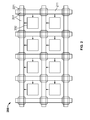
- FIG. 2 shows an example of a basic virtual fabric in accordance with embodiments of the invention
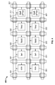
- FIG. 3 shows an example of a more mathematically complex virtual fabric in accordance with embodiments of the invention
- FIG. 4 shows an example of a virtual fabric in accordance with embodiments of the invention including soft microprocessor blocks
- FIG. 5 shows a control-data flow graph used in methods including methods according to embodiments of the invention
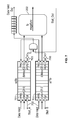
- FIG. 6 shows an example of a virtual routing switch configured in a virtual fabric according to embodiments of the invention
- FIG. 7 shows an example of a function block with virtual FIFOs configured in a virtual fabric according to embodiments of the invention.
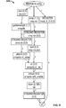
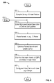
- FIG. 8 shows a flow diagram of an embodiment of a method according to embodiments of the invention for using a library of virtual fabrics to configure a programmable device
- FIG. 9 shows a flow diagram of an embodiment of another method according to embodiments of the invention for using a library of virtual fabrics to configure a programmable device
- FIG. 10 is a cross-sectional view of a magnetic data storage medium encoded with a set of machine-executable instructions for performing the method according to the present invention
- FIG. 11 is a cross-sectional view of an optically readable data storage medium encoded with a set of machine executable instructions for performing the method according to the present invention.
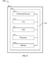
- FIG. 12 is a simplified block diagram of an illustrative system employing a programmable logic device incorporating the present invention.
- an application is executed in two parts -- a host and a kernel.
- the host is a program responsible for processing I/O requests and setting up data for parallel processing.
- When the host is ready to process data, it can launch a set of threads on a kernel, which represents a unit of computation to be performed by each thread.
- Each thread executes a kernel computation by loading data from memory as specified by the host, processing those data, and then storing the results back in memory to be read by the user, or by the user's application.
- a kernel and the data on which it is executing are considered a thread.
- Results may be computed for a group of threads at one time. Threads may be grouped into workgroups, which allow data to be shared between the threads in a workgroup. Normally, no constraints are placed on the order of execution of threads in a workgroup.
- each kernel may have access to more than one type of memory -- e.g., global memory shared by all threads, local memory shared by threads in the same workgroup, and private memory used only by a single thread.
- Execution of an OpenCL application may occur partially in the host program and partially by executing one or more kernels.
- the data arrays representing the vectors may be set up using the host program, while the actual addition may be performed using one or more kernels.
- the communication between these two parts of the application may facilitated by a set of OpenCL functions in the host program. These functions define an interface between the host and the kernel, allowing the host program to control what data is processed and when that processing begins, and to detect when the processing has been completed.
- a programmable device such as an FPGA may be programmed using a high-level language such as OpenCL by starting with a set of kernels and a host program.
- the kernels are compiled into hardware circuit representations using a Low-Level Virtual Machine (LLVM) compiler that may be extended for this purpose.
- the compilation process begins with a high-level parser, such as a C-language parser, which produces an intermediate representation for each kernel.
- the intermediate representation may be in the form of instructions and dependencies between them. This representation may then be optimized to a target programmable device.
- An optimized LLVM intermediate representation is then converted into a hardware-oriented data structure, such as a Control-Data Flow Graph (CDFG) ( FIG. 5 ).
- This data structure represents the kernel at a low level, and contains information about its area and maximum clock frequency.
- the CDFG can then be optimized to improve area and performance of the system, prior to RTL generation which produces a Verilog HDL description of each kernel.
- the compiled kernels are then instantiated in a system that preferably contains an interface to the host as well as a memory interface.
- the host interface allows the host program to access each kernel. This permits setting workspace parameters and kernel arguments remotely.
- the memory serves as global memory space for an OpenCL kernel. This memory can be accessed via the host interface, allowing the host program to set data for kernels to process and retrieve computation results.
- the host program may be compiled using a regular compiler for the high-level language in which it is written (e.g., C++).
- each kernel is implemented from basic block modules.
- Each basic block module comprises an input and an output interface with which it talks to other basic blocks, and implements an instruction such as load, add, subtract, store, etc.
- each basic block module is responsible for handling the operations inside of it.
- a basic block module also should to be able to exchange information with other basic blocks. Determining what data each basic block requires and produces may be accomplished using Live-Variable Analysis.
- a Control-Data Flow Graph ( FIG. 5 ) can be created to represent the operation of that basic block module, showing how that basic block module takes inputs either from kernel arguments or another basic block, based on the results of the Live-Variable Analysis.
- Each basic block once instantiated, processes the data according to the instructions contained within the block and produces output that can be read by other basic blocks, or directly by a user.
- each basic block module has be represented as a CDFG
- operations inside the block can be scheduled.
- Each node may be allocated a set of registers and clock cycles that it requires to complete an operation. For example, an AND operation may require no registers, but a floating-point addition may require at least seven clock cycles and corresponding registers.
- pipelining registers may be inserted to balance the latency of each path through the CDFG. This allows many threads to be processed.
- a design may be created including the kernels as well as memories and an interface to the host platform.
- the number of threads allowed in a workgroup, and the number of workgroups allowed simultaneously in a kernel may be limited.
- path 101 shows the implementation of a kernel while path 102 shows the implementation of a host program.
- Path 101 starts with a kernel file (kernel.cl) 111.
- Parser front end 121 derives unoptimized intermediate representation 131 from kernel file 111, which is converted by optimizer 141 to an optimized intermediate representation 151.
- the optimization process includes compiler techniques to make the code more efficient, such as, e.g., loop unrolling, memory-to-register conversion, dead code elimination, etc.
- a Register Timing Language (RTL) 161 generator converts optimized intermediate representation 151 into a hardware description language representation 171, which may be written in any hardware description language such as Verilog (shown) or VHDL.
- Path 102 starts with a host program file (host.c) 112 which is compiled by a compiler 122 using runtime library 132, which includes software routines that abstract the communication between the host and the programmable device, to create an executable program file 142.
- host.c host program file
- runtime library 132 which includes software routines that abstract the communication between the host and the programmable device, to create an executable program file 142.
- Executable program file 142 and hardware description language representation(s) 171 of the kernel(s) are compiled into a programmable device configuration by appropriate software 103.
- software 103 might be the QUARTUS ® II software provided by Altera.
- the result is a programmable device configured to run a host program on kernel files to instantiate circuits represented by the kernels.
- the programmable device should have an embedded processor to execute program file 142 to execute kernel(s) 111 to generate hardware description language representation(s) 161. If the embedded processor is a "soft" processor, it also may be configured using software 103. If the embedded processor is a "hard” processor, software 103 configures the appropriate connections to the hard processor.
- the required compile time can compare unfavorably to that required for convention hardware-description-language-based programming.
- compilation may take hours or even days, as compared to seconds or minutes for HDL-based programming.
- the problem of long compile times may be magnified by the need to periodically change a logic design, particularly during development.
- Each such virtual fabric 200 may be a high-level language representation of a coarse-grained virtual FPGA including an interconnect network 201 of buses 211 and routing switches 221, and a relatively smaller number of more complex function blocks 202 representing combinations of logic elements, implemented on top of a physical FPGA having a relatively larger number of individual logic elements.
- function blocks 202 may include blocks for performing basic mathematical functions such as fixed- or floating-point additions or multiplications, or trigonometric functions, as well as multiplexing logic or even "soft" microprocessors.
- the plurality of virtual fabrics may be considered a library of virtual fabrics. Different virtual fabrics in the library may have different distributions of different types of function blocks.
- the library may include a plurality of different basic virtual fabrics, of which fabric 200 is just one example, each of which has a different distribution of function blocks 202 including basic mathematical functions along with multiplexing logic.
- register stages may be provided in the virtual routing switches, each of which may be thought of as a multiplexer followed by a register.
- Any element in the pipeline preferably has the ability to stall the pipeline -- i.e., to stop the flow of data until it is ready to accept more -- by sending a stall signal upstream. Otherwise, data might be lost if upstream elements continue to send data while a downstream element is too busy to be able to process it.
- the stall signal preferably is itself pipelined, thereby providing a pipelined stall signal network within the virtual fabric. This may be achieved by providing, in some or all routing switches, a register for the stall signal. Then, instead of sending out the stall signal from the stalled component, the stall signal may be sent from the register.
- FIG. 6 An example is shown in FIG. 6 . All of the components of FIG. 6 are virtual - i.e., they are configured from the basic elements of the underlying FPGA or other configurable or programmable device as part of the compilation of the virtual fabric.
- FIG. 6 is a diagram of one possible detailed implementation of a routing switch 600, in which a signal comes in at 601 from the "west” and is routable out to the "north” at 602, to the "south” at 603, or to the "east” at 604. Routing switch 600 needs to be able to send a stall signal back upstream at 605, while receiving stall signals from the north at 606, from the south at 607 and from the east at 608.
- Virtual routing switch 600 includes an input multiplexer 611 and output multiplexers 612, 613, 614 on the north, south and east outputs, respectively. Such a routing switch might need to send a stall signal 605 back in the direction from which the input arrived, as well as receive stall signals 606, 607, 608 from any of the three output directions.
- a stall signal register 615 may be provided to output the stall signal 605, and stall signal registers 616, 617, 618 may be provided to register the received stall signals 606, 607, 608.
- Stall signal registers 615, 616, 617, 618 allow for fully pipelined stall signal propagation both upstream and downstream.
- Registers 609, 610 are provided for the input data.
- Register 609 captures the data that cannot be propagated further because of a stall being received from downstream. If any of the output directions 602, 603, 604 to which data are to be propagated is stalled, those data will be held in register 609 until the stall is cleared.
- Register 610 captures input data and prevents those data from being lost in case a stall signal 605 has to be asserted. In the absence of register 610, because of the aforementioned one-clock delay, new data would be received at multiplexer 611 on the first clock cycle after the assertion of stall signal 605 and would replace at multiplexer 611 any data previously received, even though the data previously received had not been propagated downstream.
- Configuration registers 626, 627, 628 may be provided to turn on or off the ability to receive stall signals.
- Configuration register 629 selects the input to multiplexer 611, and therefore to virtual routing switch 600.
- Configuration registers 630, 631, 632 control output multiplexers 612, 613, 614 to select one or more outputs of virtual routing switch 600.
- the pipelining of the virtual fabric also may include registers for the data themselves on the inputs of individual function blocks 202, 301, 401 of the virtual fabric. Because the lengths of the datapaths to be pipelined are unknown at the time of creation of the virtual fabrics, and different datapaths to the same function block, as implemented in a particular user design, may differ, the data pipeline registers at the inputs of each function block 202, 301, 401 preferably are FIFOs 701 as shown in FIG. 7 , to balance the pipelines.
- each FIFO 701 may be selected based on the maximum expected pipeline imbalance. However, it is possible that a FIFO 701 may fill up, and therefore each FIFO 701 has the ability to assert a stall signal 702 when full.
- each FIFO 701 also may have the ability to assert an empty signal 703 to stall function block 202, 301, 401 so that function block 202, 301, 401 does not try read data when none are available. Otherwise, the various input pipelines to function block 202, 301, 401 may get out of sync - i.e., if function block 202, 301, 401 reads data from two or more pipelines when the data on one pipeline have not yet arrived.
- a programmable device may be configured by selecting from among a library or collection of previously compiled virtual fabrics.
- the selection of a particular virtual fabric may be carried out by programming software by examining the functional needs of the user's logic design and selecting the virtual fabric that most closely matches those functional needs in terms of numbers and types of virtual function blocks. That virtual fabric is executed on the device, either by an on-board hard processor, by a soft processor that is configured on board before, after or during selection of the virtual fabric, or by an external processor. Execution of the selected virtual fabric configures the device as a coarser-grained virtual device. Conventional synthesis, placement and routing tools could then be used to configure that coarser-grained virtual device with the user's logic design.
- An embodiment of the process 800, diagrammed in FIG. 8 may begin at step 801 with the creation of a collection of compiled virtual fabrics having different sizes, as well as different distributions of functions blocks of various types as described above.
- Step 801 could be performed by the device manufacturer and the library of virtual fabrics could be provided in a memory on the device or in a storage device or medium associated with device configuration software provided with the device.
- a third party also may provide the library of compiled virtual fabrics.
- the user may compile a library of virtual fabrics the first time the device is configured.
- process 800 continues at step 803.
- a user who has compiled the user's own library of virtual fabrics process 800 continues at step 803.
- the user enters process 800 at 802 and proceeds to step 803.
- the user enters a desired configuration in the form of high-level language statements, such as OpenCL statements, as described above, defining a set of kernels.
- the kernels are parsed using a high-level parser, such as a C-language parser, which produces an intermediate representation for each kernel.
- the intermediate representation may be in the form of instructions and dependencies between them.
- this representation may then be optimized and converted into a hardware-oriented data structure, such as a Control-Data Flow Graph (CDFG).
- CDFG Control-Data Flow Graph
- the CDFG is examined by the programming software to ascertain its hardware needs, and the software then selects a virtual fabric, from among the library of virtual fabrics, that meets those hardware needs.
- the software may examine all virtual fabrics to find the best virtual fabric, or the examination may end once a virtual fabric is found that is sufficiently close to the hardware needs.
- "sufficiently close” means that all of the required resources are present in the virtual fabric, but the virtual fabric may have additional resources that may go unused.
- step 807 the user's logic design is programmed onto the selected virtual fabric from the CDFG using conventional synthesis, placement and routing techniques, such as those that may be implemented by the aforementioned QUARTUS ® II software available from Altera Corporation.
- this step may include configuring a soft processor to execute the virtual fabric.
- a particular user logic design may include a large number of functions not all of which are active at the same time. Because virtual fabrics as described herein are relatively coarse, they have a relatively small number of configuration bits. Therefore, it may not be impractical (in terms of execution time) to allow reconfiguration of the virtual fabric at run-time.
- the virtual fabric may be configured with a first configuration including a first group of functions, and then, "on the fly,” may be reconfigured with a second group of functions (which may overlap the first group of functions -- i.e., it may have some functions in common with the first group of functions).
- Method 850 for programming a device to use such reconfiguration is shown in FIG. 9 .
- Method 850 starts out similarly to method 800, with steps 801, 802, 803, 804 and 805.
- the CDFG is examined to ascertain its hardware needs, and the software then selects a virtual fabric, from among the library of virtual fabrics, that can meet those hardware needs in two or more separate configurations. For example, one way of deciding which virtual fabric to use would be to use a cost function that computes how closely the virtual fabric resembles the resource needs of the kernel.
- the two or more separate configurations are programmed using conventional synthesis, placement and routing techniques, such as those that may be implemented by the aforementioned QUARTUS ® II software.
- the configuration bitstreams for the various configurations are stored at step 858, and the virtual fabric is configured at step 859 with the first configuration.
- that configuration may be unloaded at step 862 and another one of the two or more configurations may be loaded at step 863.
- the method returns to step 859 as the new configuration is executed. This may happen more than once as various ones of the two or more configurations are unloaded and reloaded until the desired function of the device has been accomplished.
- the reconfiguration process can be used regardless of whether he physical device supports reconfiguration on-the-fly. It is only necessary that the virtual device represented by the virtual fabric support reconfiguration on-the-fly. It will be further appreciated that if the physical device supports reconfiguration on-the-fly, then not only can the configuration of a selected virtual fabric be changed at run time, but the virtual fabrics themselves can be unloaded and loaded on-the-fly (with configurations of any particular virtual fabric that is loaded being changed on-the-fly, if needed, as described above).
- the virtual fabrics in the library are compiled ahead of time into hardware description language representations, only the user's high-level synthesis language representation of the desired configuration of the virtual fabric need be compiled as part of the user programming process.
- the user still enters the complete high-level description of the desired circuit, and there still will be a processor present to execute that high-level description to create a configured device.
- the only compilation involved will be the compilation of the configuration of the virtual fabric, which, as noted above, involves only a relatively small configuration problem. Therefore, the compilation time seen by the user is much shorter than what would be required if the entire design were to be compiled from the high-level description, and is comparable to configuration times when using hardware description languages.
- Instructions for carrying out a method according to this invention for programming a programmable device may be encoded on a machine-readable medium, to be executed by a suitable computer or similar device to implement the method of the invention for programming or configuring PLDs or other programmable devices with a configuration described by a high-level synthesis language as described above.
- a personal computer may be equipped with an interface to which a PLD can be connected, and the personal computer can be used by a user to program the PLD using suitable software tools as described above.
- the same machine-readable medium, or a separate machine-readable medium may be encoded with the library of virtual fabrics.
- FIG. 10 presents a cross section of a magnetic data storage medium 1200 which can be encoded with a machine executable program that can be carried out by systems such as the aforementioned personal computer, or other computer or similar device, or encoded with a library of virtual fabrics.
- Medium 1200 can be a floppy diskette or hard disk, or magnetic tape, having a suitable substrate 1201, which may be conventional, and a suitable coating 1202, which may be conventional, on one or both sides, containing magnetic domains (not visible) whose polarity or orientation can be altered magnetically. Except in the case where it is magnetic tape, medium 1200 may also have an opening (not shown) for receiving the spindle of a disk drive or other data storage device.
- the magnetic domains of coating 1202 of medium 1200 are polarized or oriented so as to encode, in manner which may be conventional, a machine-executable program, for execution by a programming system such as a personal computer or other computer or similar system, having a socket or peripheral attachment into which the PLD to be programmed may be inserted, to configure appropriate portions of the PLD, including its specialized processing blocks, if any, in accordance with the invention.
- FIG. 11 shows a cross section of an optically-readable data storage medium 1210 which also can be encoded with such a machine-executable program, which can be carried out by systems such as the aforementioned personal computer, or other computer or similar device, or encoded with a library of virtual fabrics.
- Medium 1210 can be a conventional compact disk read-only memory (CD-ROM) or digital video disk read-only memory (DVD-ROM) or a rewriteable medium such as a CD-R, CD-RW, DVD-R, DVD-RW, DVD+R, DVD+RW, or DVD-RAM or a magneto-optical disk which is optically readable and magneto-optically rewriteable.
- Medium 1210 preferably has a suitable substrate 1211, which may be conventional, and a suitable coating 1212, which may be conventional, usually on one or both sides of substrate 1211.
- coating 1212 is reflective and is impressed with a plurality of pits 1213, arranged on one or more layers, to encode the machine-executable program.
- the arrangement of pits is read by reflecting laser light off the surface of coating 1212.
- a protective coating 1214 which preferably is substantially transparent, is provided on top of coating 1212.
- coating 1212 has no pits 1213, but has a plurality of magnetic domains whose polarity or orientation can be changed magnetically when heated above a certain temperature, as by a laser (not shown).
- the orientation of the domains can be read by measuring the polarization of laser light reflected from coating 1212.
- the arrangement of the domains encodes the program as described above.
- a PLD 1500 programmed according to the present invention may be used in many kinds of electronic devices.
- Data processing system 1400 may include one or more of the following components: a processor 1401; memory 1402; I/O circuitry 1403; and peripheral devices 1404. These components are coupled together by a system bus 1405 and are populated on a circuit board 1406 which is contained in an end-user system 1407.
- System 1400 can be used in a wide variety of applications, such as computer networking, data networking, instrumentation, video processing, digital signal processing, or any other application where the advantage of using programmable or reprogrammable logic is desirable.
- PLD 140 can be used to perform a variety of different logic functions.
- PLD 1500 can be configured as a processor or controller that works in cooperation with processor 1401.
- PLD 1500 may also be used as an arbiter for arbitrating access to a shared resources in system 1400.
- PLD 1500 can be configured as an interface between processor 1401 and one of the other components in system 1400. It should be noted that system 1400 is only exemplary, and that the true scope and spirit of the invention should be indicated by the following claims.
Landscapes
- Engineering & Computer Science (AREA)
- Computer Hardware Design (AREA)
- Physics & Mathematics (AREA)
- Theoretical Computer Science (AREA)
- General Engineering & Computer Science (AREA)
- General Physics & Mathematics (AREA)
- Geometry (AREA)
- Evolutionary Computation (AREA)
- Computer Networks & Wireless Communication (AREA)
- Mathematical Physics (AREA)
- Signal Processing (AREA)
- Computing Systems (AREA)
- Logic Circuits (AREA)
Abstract
Description
- This invention relates to the use of a high-level language to configure a programmable integrated circuit devices such as a field-programmable gate array (FPGAs) or other type of programmable logic devices (PLDs).
- Early programmable devices were one-time configurable. For example, configuration may have been achieved by "blowing" - i.e., opening - fusible links. Alternatively, the configuration may have been stored in a programmable read-only memory. Those devices generally provided the user with the ability to configure the devices for "sum-of-products" (or "P-TERM") logic operations. Later, such programmable logic devices incorporating erasable programmable read-only memory (EPROM) for configuration became available, allowing the devices to be reconfigured.
- Still later, programmable devices incorporating static random access memory (SRAM) elements for configuration became available. These devices, which also can be reconfigured, store their configuration in a nonvolatile memory such as an EPROM, from which the configuration is loaded into the SRAM elements when the device is powered up. These devices generally provide the user with the ability to configure the devices for look-up-table-type logic operations.
- At some point, such devices began to be provided with embedded blocks of random access memory that could be configured by the user to act as random access memory, read-only memory, or logic (such as P-TERM logic). Moreover, as programmable devices have become larger, it has become more common to add dedicated circuits on the programmable devices for various commonly-used functions. Such dedicated circuits could include phase-locked loops or delay-locked loops for clock generation, as well as various circuits for various mathematical operations such as addition or multiplication. This spares users from having to create equivalent circuits by configuring the available general-purpose programmable logic.
- While it may have been possible to configure the earliest programmable logic devices manually, simply by determining mentally where various elements should be laid out, it was common even in connection with such earlier devices to provide programming software that allowed a user to lay out logic as desired and then translate that logic into a configuration for the programmable device. With current larger devices, including those with the aforementioned dedicated circuitry, it would be impractical to attempt to lay out the logic without such software. Such software also now commonly includes pre-defined functions, commonly referred to as "cores," for configuring certain commonly-used structures, and particularly for configuring circuits for mathematical operations incorporating the aforementioned dedicated circuits. For example, cores may be provided for various trigonometric or algebraic functions.
- Although available programming software allows users to implement almost any desired logic design within the capabilities of the device being programmed, most such software requires knowledge of hardware description languages such as VHDL or Verilog. However, many potential users of programmable devices are not well-versed in hardware description languages and may prefer to program devices using a higher-level programming language.
- One high-level programming language that may be adopted for configuring a programmable device is OpenCL (Open Computing Language), although use of other high-level languages, and particularly other high-level synthesis languages, including C, C++, Fortran, C#, F#, BlueSpec and Matlab, also is within the scope of this invention.
- In OpenCL, computation is performed using a combination of a host and kernels, where the host is responsible for input/output (I/O) and setup tasks, and kernels perform computation on independent inputs. Where there is explicit declaration of a kernel, and each set of elements to be processed is known to be independent, each kernel can be implemented as a high-performance hardware circuit. Based on the amount of space available on a programmable device such as an FPGA, the kernel may be replicated to improve performance of an application.
- A kernel compiler converts a kernel into a hardware circuit, implementing an application from an OpenCL description, through hardware generation, system integration, and interfacing with a host computer. The compiler may be based on an open-source Low-Level Virtual Machine compiler extended to enable compilation of OpenCL applications. The compiler parses, analyzes, optimizes and implements an OpenCL kernel as a high-performance pipelined circuit, suitable for implementation on programmable device such as an FPGA. The system may then be compiled using programming tools appropriate for the particular programmable device. The device also has an embedded hard processor or may be configured with an embedded soft processor, to run the OpenCL (or other high-level) code, or an external processor may be used. The OpenCL or other high-level code can be run by executing the host program on the embedded or external processor.
- In accordance with an exemplary embodiment of the invention there is provided a method of preparing a programmable integrated circuit device for configuration using a high-level language. The method includes compiling a plurality of virtual programmable devices from descriptions in said high-level language. That compiling includes compiling configurations of configurable routing resources from programmable resources of said programmable integrated circuit device, and compiling configurations of a plurality of complex function blocks from programmable resources of said programmable integrated circuit device.
- In one exemplary embodiment, said high-level language is OpenCL.
- In a further exemplary embodiment of the invention, said compiling configurations of configurable routing resources comprises compiling a pipelined stall signal network.
- For example, in one exemplary implementation of this embodiment, said compiling a pipelined stall signal network comprises compiling a bidirectional stall signal network that is pipelined in both directions.
- In another exemplary implementation of this embodiment, said compiling a pipelined stall signal network comprises compiling a network including a plurality of routing switches. Each of said routing switches may have an input and at least one output; a respective register for a stall signal on each of said input and said at least one output; an output data stall register for storing output data during a stall of any of said at least one output; a first input data stall register for storing data received at said input prior to a stall of said input; and a second input data stall register for storing data present at said input when said input stalls.
- Furthermore, in another embodiment of the invention said plurality of complex function blocks comprises at least one of an arithmetic function block, a trigonometric function block, a multiplexing logic block, or a soft processor block.
- In a further embodiment of the invention, the method further comprises configuring input registers for at least one complex function block of said plurality of complex function blocks for balancing said configurable routing resources.
- For example, in one exemplary implementation of this embodiment, said configuring input registers may comprise configuring a respective FIFO on at least one input of said at least one complex function block of said plurality of complex function blocks.
- Further, said configuring input registers may optionally comprise configuring a respective FIFO on each input of each complex function block of said plurality of complex function blocks.
- Alternatively, said configuring a respective FIFO may optionally comprise configuring a respective FIFO having a respective depth equal to a respective maximum expected pipeline imbalance.
- In another embodiment of the invention, said compiling a plurality of virtual programmable devices comprises compiling at least one virtual programmable device that is reconfigurable during operation.
- Another embodiment of the invention provides a non-transitory machine readable storage medium. The storage medium may be encoded with a plurality of compiled configurations for a programmable integrated circuit device. Each of said compiled configurations is capable of causing a processor to instantiate on said programmable integrated circuit device a respective virtual programmable device by executing a high-level synthesis language. In this embodiment, each said respective virtual programmable device comprises a respective routing resource configuration; and configurations for a plurality of complex function blocks.
- In the non-transitory machine readable storage medium of a further embodiment of the invention each respective routing resource configuration instantiates a pipelined stall signal network.
- In another non-transitory machine readable storage medium of a further embodiment of the invention each respective routing resource configuration instantiates a bidirectional stall signal network that is pipelined in both directions.
- In yet another non-transitory machine readable storage medium of an exemplary embodiment of the invention each respective routing resource configuration instantiates a pipelined stall signal network including a plurality of routing switches. Each of said routing switches may have an input and at least one output; a respective register for a stall signal on each of said input and said at least one output; an output data stall register for storing output data during a stall of any of said at least one output; a first input data stall register for storing data received at said input prior to a stall of said input; and a second input data stall register for storing data present at said input when said input stalls.
- In a further exemplary embodiment of the invention, said configurations for a plurality of complex function blocks comprise configurations for at least one of an arithmetic function block, a trigonometric function block, a multiplexing logic block, or a soft processor block.
- In another non-transitory machine readable storage medium of a further embodiment of the invention, said configurations for a plurality of complex function blocks comprise configurations for input registers for at least one of said plurality of complex function blocks for balancing said configurable routing resources.
- In one exemplary implementation of this embodiment of the non-transitory machine readable storage medium said configurations for input registers comprise configurations for a respective FIFO on at least one input of said at least one of said plurality of complex function blocks.
- For example, said configurations for input registers may comprise configurations for a respective FIFO on each input of each of said plurality of complex function blocks.
- In another example, said configurations for a respective FIFO may comprise configurations for a respective FIFO having a respective depth equal to a respective maximum expected pipeline imbalance.
- In the non-transitory machine readable storage medium of another exemplary embodiment of the invention wherein said plurality of compiled configurations for a plurality of virtual programmable devices comprises at least one compiled configuration for a virtual programmable device that is reconfigurable during operation.
- Another embodiment of the invention provides a routing switch for use in a network in which stall signals control flow of signals. The routing switch comprises an input for receiving data from elsewhere in said network; an input stall signal output for propagating an input stall signal to prevent data from being propagated to said input from elsewhere in said network; a plurality of respective outputs for propagating data to respective other locations in said network; and a respective output stall signal input associated with each said respective output for receiving a respective output stall signal from a respective one of said other locations to prevent said respective output from propagating data to said respective one of said other locations.
- In another exemplary embodiment of the invention, the routing switch further comprises an input stall signal register for said input stall signal; and a respective output stall signal register for each of said respective output stall signals.
- In a further exemplary embodiment of the invention, the routing switch further comprises an input data register for holding data received prior to assertion of one of said output stall signals until said data received prior to assertion of said one of said output stall signals can be propagated.
- Another exemplary embodiment of the invention relates to a machine-readable data storage medium encoded with a library of such compiled configurations also is provided, as is a routing switch that may be used in a virtual programmable device or any programmable device.
- Further features of the invention, its nature and various advantages will be apparent upon consideration of the following detailed description, taken in conjunction with the accompanying drawings, in which like reference characters refer to like parts throughout, and in which:
-
FIG. 1 shows a known method for using a high-level language to configure a programmable device; -
FIG. 2 shows an example of a basic virtual fabric in accordance with embodiments of the invention; -
FIG. 3 shows an example of a more mathematically complex virtual fabric in accordance with embodiments of the invention; -
FIG. 4 shows an example of a virtual fabric in accordance with embodiments of the invention including soft microprocessor blocks; -
FIG. 5 shows a control-data flow graph used in methods including methods according to embodiments of the invention; -
FIG. 6 shows an example of a virtual routing switch configured in a virtual fabric according to embodiments of the invention; -
FIG. 7 shows an example of a function block with virtual FIFOs configured in a virtual fabric according to embodiments of the invention; -
FIG. 8 shows a flow diagram of an embodiment of a method according to embodiments of the invention for using a library of virtual fabrics to configure a programmable device; -
FIG. 9 shows a flow diagram of an embodiment of another method according to embodiments of the invention for using a library of virtual fabrics to configure a programmable device; -
FIG. 10 is a cross-sectional view of a magnetic data storage medium encoded with a set of machine-executable instructions for performing the method according to the present invention; -
FIG. 11 is a cross-sectional view of an optically readable data storage medium encoded with a set of machine executable instructions for performing the method according to the present invention; and -
FIG. 12 is a simplified block diagram of an illustrative system employing a programmable logic device incorporating the present invention. - In OpenCL, an application is executed in two parts -- a host and a kernel. The host is a program responsible for processing I/O requests and setting up data for parallel processing. When the host is ready to process data, it can launch a set of threads on a kernel, which represents a unit of computation to be performed by each thread.
- Each thread executes a kernel computation by loading data from memory as specified by the host, processing those data, and then storing the results back in memory to be read by the user, or by the user's application. In OpenCL terminology, a kernel and the data on which it is executing are considered a thread. Results may be computed for a group of threads at one time. Threads may be grouped into workgroups, which allow data to be shared between the threads in a workgroup. Normally, no constraints are placed on the order of execution of threads in a workgroup.
- For the purposes of data storage and processing, each kernel may have access to more than one type of memory -- e.g., global memory shared by all threads, local memory shared by threads in the same workgroup, and private memory used only by a single thread.
- Execution of an OpenCL application may occur partially in the host program and partially by executing one or more kernels. For example, in vector addition, the data arrays representing the vectors may be set up using the host program, while the actual addition may be performed using one or more kernels. The communication between these two parts of the application may facilitated by a set of OpenCL functions in the host program. These functions define an interface between the host and the kernel, allowing the host program to control what data is processed and when that processing begins, and to detect when the processing has been completed.
- A programmable device such as an FPGA may be programmed using a high-level language such as OpenCL by starting with a set of kernels and a host program. The kernels are compiled into hardware circuit representations using a Low-Level Virtual Machine (LLVM) compiler that may be extended for this purpose. The compilation process begins with a high-level parser, such as a C-language parser, which produces an intermediate representation for each kernel. The intermediate representation may be in the form of instructions and dependencies between them. This representation may then be optimized to a target programmable device.
- An optimized LLVM intermediate representation is then converted into a hardware-oriented data structure, such as a Control-Data Flow Graph (CDFG) (
FIG. 5 ). This data structure represents the kernel at a low level, and contains information about its area and maximum clock frequency. The CDFG can then be optimized to improve area and performance of the system, prior to RTL generation which produces a Verilog HDL description of each kernel. - The compiled kernels are then instantiated in a system that preferably contains an interface to the host as well as a memory interface. The host interface allows the host program to access each kernel. This permits setting workspace parameters and kernel arguments remotely. The memory serves as global memory space for an OpenCL kernel. This memory can be accessed via the host interface, allowing the host program to set data for kernels to process and retrieve computation results. Finally, the host program may be compiled using a regular compiler for the high-level language in which it is written (e.g., C++).
- Returning to individual parts of the process, to compile kernels into a hardware circuit, each kernel is implemented from basic block modules. Each basic block module comprises an input and an output interface with which it talks to other basic blocks, and implements an instruction such as load, add, subtract, store, etc.
- The next step in implementing each kernel as a hardware circuit is to convert each basic block module into a hardware module. Each basic block module is responsible for handling the operations inside of it. To function properly, a basic block module also should to be able to exchange information with other basic blocks. Determining what data each basic block requires and produces may be accomplished using Live-Variable Analysis.
- Once each basic block is analyzed, a Control-Data Flow Graph (CDFG) (
FIG. 5 ) can be created to represent the operation of that basic block module, showing how that basic block module takes inputs either from kernel arguments or another basic block, based on the results of the Live-Variable Analysis. Each basic block, once instantiated, processes the data according to the instructions contained within the block and produces output that can be read by other basic blocks, or directly by a user. - Once each basic block module has be represented as a CDFG, operations inside the block can be scheduled. Each node may be allocated a set of registers and clock cycles that it requires to complete an operation. For example, an AND operation may require no registers, but a floating-point addition may require at least seven clock cycles and corresponding registers. Once each basic block is scheduled, pipelining registers may be inserted to balance the latency of each path through the CDFG. This allows many threads to be processed.
- Once each kernel has been described as a hardware circuit, a design may be created including the kernels as well as memories and an interface to the host platform. To prevent pipeline overload, the number of threads allowed in a workgroup, and the number of workgroups allowed simultaneously in a kernel, may be limited.
- The foregoing
generalized method 100 is diagrammed inFIG. 1 wherepath 101 shows the implementation of a kernel whilepath 102 shows the implementation of a host program. -
Path 101 starts with a kernel file (kernel.cl) 111. Parserfront end 121 derives unoptimizedintermediate representation 131 fromkernel file 111, which is converted byoptimizer 141 to an optimizedintermediate representation 151. The optimization process includes compiler techniques to make the code more efficient, such as, e.g., loop unrolling, memory-to-register conversion, dead code elimination, etc. A Register Timing Language (RTL) 161 generator converts optimizedintermediate representation 151 into a hardwaredescription language representation 171, which may be written in any hardware description language such as Verilog (shown) or VHDL. -
Path 102 starts with a host program file (host.c) 112 which is compiled by acompiler 122 usingruntime library 132, which includes software routines that abstract the communication between the host and the programmable device, to create anexecutable program file 142. -
Executable program file 142 and hardware description language representation(s) 171 of the kernel(s) are compiled into a programmable device configuration byappropriate software 103. For example, for FPGA devices available from Altera Corporation, of San Jose, California,software 103 might be the QUARTUS® II software provided by Altera. - The result is a programmable device configured to run a host program on kernel files to instantiate circuits represented by the kernels. The programmable device should have an embedded processor to execute program file 142 to execute kernel(s) 111 to generate hardware description language representation(s) 161. If the embedded processor is a "soft" processor, it also may be configured using
software 103. If the embedded processor is a "hard" processor,software 103 configures the appropriate connections to the hard processor. - Although the foregoing generalized method can be used to create efficient hardware circuit implementations of user logic designs using a high-level language, such as OpenCL, the required compile time can compare unfavorably to that required for convention hardware-description-language-based programming. Depending on the particular user logic design, compilation may take hours or even days, as compared to seconds or minutes for HDL-based programming. The problem of long compile times may be magnified by the need to periodically change a logic design, particularly during development.
- Therefore, in accordance with the present invention, a plurality of high-level language representations of "virtual fabrics" may be precompiled. Each such virtual fabric 200 (
FIG. 2 ) may be a high-level language representation of a coarse-grained virtual FPGA including aninterconnect network 201 ofbuses 211 androuting switches 221, and a relatively smaller number of more complex function blocks 202 representing combinations of logic elements, implemented on top of a physical FPGA having a relatively larger number of individual logic elements. For example, function blocks 202 may include blocks for performing basic mathematical functions such as fixed- or floating-point additions or multiplications, or trigonometric functions, as well as multiplexing logic or even "soft" microprocessors. - The plurality of virtual fabrics may be considered a library of virtual fabrics. Different virtual fabrics in the library may have different distributions of different types of function blocks. For example, the library may include a plurality of different basic virtual fabrics, of which
fabric 200 is just one example, each of which has a different distribution of function blocks 202 including basic mathematical functions along with multiplexing logic. There may also be some more complex virtual fabrics, of which fabric 300 (FIG. 3 ) is just one example, having the basic and multiplexing functions 202, but in which various function blocks 301 are for performing more complex functions such as trigonometric functions. As between different ones of those more complex virtual fabrics, the numbers and distributions of the various arithmetic, trigonometric and multiplexing functions may vary. There may even be virtual fabrics, of which fabric 400 (FIG. 4 ) is just one example, which may be similar tofabric 200 orfabric 300, except that one or more function blocks are replaced by soft processor blocks 401. Additional types of virtual fabrics also may be provided. - It may be desirable to speed up the performance of a virtual fabric by pipelining it to some degree. For example, register stages may be provided in the virtual routing switches, each of which may be thought of as a multiplexer followed by a register. Any element in the pipeline preferably has the ability to stall the pipeline -- i.e., to stop the flow of data until it is ready to accept more -- by sending a stall signal upstream. Otherwise, data might be lost if upstream elements continue to send data while a downstream element is too busy to be able to process it.
- However, if an element sends a stall signal upstream, it might arrive one clock cycle too late, so that one clock cycle's worth of data might be lost. Therefore, the stall signal preferably is itself pipelined, thereby providing a pipelined stall signal network within the virtual fabric. This may be achieved by providing, in some or all routing switches, a register for the stall signal. Then, instead of sending out the stall signal from the stalled component, the stall signal may be sent from the register.
- An example is shown in
FIG. 6 . All of the components ofFIG. 6 are virtual - i.e., they are configured from the basic elements of the underlying FPGA or other configurable or programmable device as part of the compilation of the virtual fabric. -
FIG. 6 is a diagram of one possible detailed implementation of arouting switch 600, in which a signal comes in at 601 from the "west" and is routable out to the "north" at 602, to the "south" at 603, or to the "east"
at 604.Routing switch 600 needs to be able to send a stall signal back upstream at 605, while receiving stall signals from the north at 606, from the south at 607 and from the east at 608. -
Virtual routing switch 600 includes aninput multiplexer 611 andoutput multiplexers stall signal 605 back in the direction from which the input arrived, as well as receivestall signals stall signal register 615 may be provided to output thestall signal 605, and stall signal registers 616, 617, 618 may be provided to register the receivedstall signals -
Registers Register 609 captures the data that cannot be propagated further because of a stall being received from downstream. If any of theoutput directions register 609 until the stall is cleared.Register 610 captures input data and prevents those data from being lost in case astall signal 605 has to be asserted. In the absence ofregister 610, because of the aforementioned one-clock delay, new data would be received atmultiplexer 611 on the first clock cycle after the assertion ofstall signal 605 and would replace atmultiplexer 611 any data previously received, even though the data previously received had not been propagated downstream. However, with the presence ofregister 610, the data previously received atmultiplexer 611 are preserved, even though additional data have subsequently been received atmultiplexer 611. Configuration registers 626, 627, 628 may be provided to turn on or off the ability to receive stall signals.Configuration register 629 selects the input tomultiplexer 611, and therefore tovirtual routing switch 600. Configuration registers 630, 631, 632control output multiplexers virtual routing switch 600. - In addition to the pipelining of the stall signal network as just described, the pipelining of the virtual fabric also may include registers for the data themselves on the inputs of individual function blocks 202, 301, 401 of the virtual fabric. Because the lengths of the datapaths to be pipelined are unknown at the time of creation of the virtual fabrics, and different datapaths to the same function block, as implemented in a particular user design, may differ, the data pipeline registers at the inputs of each
function block FIG. 7 , to balance the pipelines. - The depth of each
FIFO 701 may be selected based on the maximum expected pipeline imbalance. However, it is possible that aFIFO 701 may fill up, and therefore eachFIFO 701 has the ability to assert astall signal 702 when full. - Similarly, each
FIFO 701 also may have the ability to assert anempty signal 703 to stallfunction block function block block function block - According to another aspect of the invention, a programmable device may be configured by selecting from among a library or collection of previously compiled virtual fabrics. The selection of a particular virtual fabric may be carried out by programming software by examining the functional needs of the user's logic design and selecting the virtual fabric that most closely matches those functional needs in terms of numbers and types of virtual function blocks. That virtual fabric is executed on the device, either by an on-board hard processor, by a soft processor that is configured on board before, after or during selection of the virtual fabric, or by an external processor. Execution of the selected virtual fabric configures the device as a coarser-grained virtual device. Conventional synthesis, placement and routing tools could then be used to configure that coarser-grained virtual device with the user's logic design.
- An embodiment of the
process 800, diagrammed inFIG. 8 may begin atstep 801 with the creation of a collection of compiled virtual fabrics having different sizes, as well as different distributions of functions blocks of various types as described above. Step 801 could be performed by the device manufacturer and the library of virtual fabrics could be provided in a memory on the device or in a storage device or medium associated with device configuration software provided with the device. A third party also may provide the library of compiled virtual fabrics. Alternatively, the user may compile a library of virtual fabrics the first time the device is configured. - For a user who has compiled the user's own library of virtual fabrics,
process 800 continues atstep 803. For a user who is using a previously-compiled library of virtual fabrics (whether provided by the manufacturer or a third party, or by the user during a previous configuring of the device), the user entersprocess 800 at 802 and proceeds to step 803. - At
step 803, the user enters a desired configuration in the form of high-level language statements, such as OpenCL statements, as described above, defining a set of kernels. As above, atstep 804, the kernels are parsed using a high-level parser, such as a C-language parser, which produces an intermediate representation for each kernel. The intermediate representation may be in the form of instructions and dependencies between them. Atstep 805, this representation may then be optimized and converted into a hardware-oriented data structure, such as a Control-Data Flow Graph (CDFG). - At
step 806, the CDFG is examined by the programming software to ascertain its hardware needs, and the software then selects a virtual fabric, from among the library of virtual fabrics, that meets those hardware needs. Using known techniques, the software may examine all virtual fabrics to find the best virtual fabric, or the examination may end once a virtual fabric is found that is sufficiently close to the hardware needs. In this context, "sufficiently close" means that all of the required resources are present in the virtual fabric, but the virtual fabric may have additional resources that may go unused. - Finally, at
step 807, the user's logic design is programmed onto the selected virtual fabric from the CDFG using conventional synthesis, placement and routing techniques, such as those that may be implemented by the aforementioned QUARTUS® II software available from Altera Corporation. Unless the device includes an embedded hard processor, or an external hard processor is to be used to execute the virtual fabric, this step may include configuring a soft processor to execute the virtual fabric. - A particular user logic design may include a large number of functions not all of which are active at the same time. Because virtual fabrics as described herein are relatively coarse, they have a relatively small number of configuration bits. Therefore, it may not be impractical (in terms of execution time) to allow reconfiguration of the virtual fabric at run-time. Thus, the virtual fabric may be configured with a first configuration including a first group of functions, and then, "on the fly," may be reconfigured with a second group of functions (which may overlap the first group of functions -- i.e., it may have some functions in common with the first group of functions).
- A
method 850 for programming a device to use such reconfiguration is shown inFIG. 9 .Method 850 starts out similarly tomethod 800, withsteps step 856, the CDFG is examined to ascertain its hardware needs, and the software then selects a virtual fabric, from among the library of virtual fabrics, that can meet those hardware needs in two or more separate configurations. For example, one way of deciding which virtual fabric to use would be to use a cost function that computes how closely the virtual fabric resembles the resource needs of the kernel. - At
step 857, the two or more separate configurations are programmed using conventional synthesis, placement and routing techniques, such as those that may be implemented by the aforementioned QUARTUS® II software. The configuration bitstreams for the various configurations are stored atstep 858, and the virtual fabric is configured atstep 859 with the first configuration. As necessary (tests 860, 861), that configuration may be unloaded atstep 862 and another one of the two or more configurations may be loaded atstep 863. The method returns to step 859 as the new configuration is executed. This may happen more than once as various ones of the two or more configurations are unloaded and reloaded until the desired function of the device has been accomplished. - It will be appreciated that because the selected virtual fabric is not being changed during the reconfiguration process just described, the reconfiguration process can be used regardless of whether he physical device supports reconfiguration on-the-fly. It is only necessary that the virtual device represented by the virtual fabric support reconfiguration on-the-fly. It will be further appreciated that if the physical device supports reconfiguration on-the-fly, then not only can the configuration of a selected virtual fabric be changed at run time, but the virtual fabrics themselves can be unloaded and loaded on-the-fly (with configurations of any particular virtual fabric that is loaded being changed on-the-fly, if needed, as described above).
- Because the virtual fabrics in the library are compiled ahead of time into hardware description language representations, only the user's high-level synthesis language representation of the desired configuration of the virtual fabric need be compiled as part of the user programming process. The user still enters the complete high-level description of the desired circuit, and there still will be a processor present to execute that high-level description to create a configured device. But because a large part of the execution of the user's high-level description will involve selection of a pre-compiled virtual fabric, the only compilation involved will be the compilation of the configuration of the virtual fabric, which, as noted above, involves only a relatively small configuration problem. Therefore, the compilation time seen by the user is much shorter than what would be required if the entire design were to be compiled from the high-level description, and is comparable to configuration times when using hardware description languages.
- Thus it is seen that a method for configuring a programmable device using a high-level synthesis language, without requiring inordinately long compilation times, has been provided.
- Instructions for carrying out a method according to this invention for programming a programmable device may be encoded on a machine-readable medium, to be executed by a suitable computer or similar device to implement the method of the invention for programming or configuring PLDs or other programmable devices with a configuration described by a high-level synthesis language as described above. For example, a personal computer may be equipped with an interface to which a PLD can be connected, and the personal computer can be used by a user to program the PLD using suitable software tools as described above. Moreover, the same machine-readable medium, or a separate machine-readable medium, may be encoded with the library of virtual fabrics.
-
FIG. 10 presents a cross section of a magneticdata storage medium 1200 which can be encoded with a machine executable program that can be carried out by systems such as the aforementioned personal computer, or other computer or similar device, or encoded with a library of virtual fabrics.Medium 1200 can be a floppy diskette or hard disk, or magnetic tape, having asuitable substrate 1201, which may be conventional, and asuitable coating 1202, which may be conventional, on one or both sides, containing magnetic domains (not visible) whose polarity or orientation can be altered magnetically. Except in the case where it is magnetic tape, medium 1200 may also have an opening (not shown) for receiving the spindle of a disk drive or other data storage device. - The magnetic domains of
coating 1202 of medium 1200 are polarized or oriented so as to encode, in manner which may be conventional, a machine-executable program, for execution by a programming system such as a personal computer or other computer or similar system, having a socket or peripheral attachment into which the PLD to be programmed may be inserted, to configure appropriate portions of the PLD, including its specialized processing blocks, if any, in accordance with the invention. -
FIG. 11 shows a cross section of an optically-readabledata storage medium 1210 which also can be encoded with such a machine-executable program, which can be carried out by systems such as the aforementioned personal computer, or other computer or similar device, or encoded with a library of virtual fabrics.Medium 1210 can be a conventional compact disk read-only memory (CD-ROM) or digital video disk read-only memory (DVD-ROM) or a rewriteable medium such as a CD-R, CD-RW, DVD-R, DVD-RW, DVD+R, DVD+RW, or DVD-RAM or a magneto-optical disk which is optically readable and magneto-optically rewriteable.
Medium 1210 preferably has asuitable substrate 1211, which may be conventional, and asuitable coating 1212, which may be conventional, usually on one or both sides ofsubstrate 1211. - In the case of a CD-based or DVD-based medium, as is well known,
coating 1212 is reflective and is impressed with a plurality ofpits 1213, arranged on one or more layers, to encode the machine-executable program. The arrangement of pits is read by reflecting laser light off the surface ofcoating 1212. Aprotective coating 1214, which preferably is substantially transparent, is provided on top ofcoating 1212. - In the case of magneto-optical disk, as is well known,
coating 1212 has nopits 1213, but has a plurality of magnetic domains whose polarity or orientation can be changed magnetically when heated above a certain temperature, as by a laser (not shown). The orientation of the domains can be read by measuring the polarization of laser light reflected fromcoating 1212. The arrangement of the domains encodes the program as described above. - A PLD 1500 programmed according to the present invention may be used in many kinds of electronic devices. One possible use is in a
data processing system 1400 shown inFIG. 12 .Data processing system 1400 may include one or more of the following components: aprocessor 1401;memory 1402; I/O circuitry 1403; andperipheral devices 1404. These components are coupled together by asystem bus 1405 and are populated on acircuit board 1406 which is contained in an end-user system 1407. -
System 1400 can be used in a wide variety of applications, such as computer networking, data networking, instrumentation, video processing, digital signal processing, or any other application where the advantage of using programmable or reprogrammable logic is desirable.PLD 140 can be used to perform a variety of different logic functions. For example, PLD 1500 can be configured as a processor or controller that works in cooperation withprocessor 1401. PLD 1500 may also be used as an arbiter for arbitrating access to a shared resources insystem 1400. In yet another example, PLD 1500 can be configured as an interface betweenprocessor 1401 and one of the other components insystem 1400. It should be noted thatsystem 1400 is only exemplary, and that the true scope and spirit of the invention should be indicated by the following claims. - Various technologies can be used to implement PLDs 1500 as described above and incorporating this invention.
- The various elements of this invention can be provided on a PLD in any desired number and/or arrangement. One skilled in the art will appreciate that the present invention can be practiced by other than the described embodiments, which are presented for purposes of illustration and not of limitation, and the present invention is limited only by the claims that follow.
Claims (14)
- A method of preparing a programmable integrated circuit device for configuration using a high-level language, said method comprising:compiling a plurality of virtual programmable devices from descriptions in said high-level language; said compiling comprising:compiling configurations of configurable routing resources from programmable resources of said programmable integrated circuit device; andcompiling configurations of a plurality of complex function blocks from programmable resources of said programmable integrated circuit device.
- The method of claim 1 wherein said high-level language is OpenCL.
- The method of claim 1 or 2 wherein said compiling configurations of configurable routing resources comprises compiling a pipelined stall signal network.
- The method of claim 3 wherein said compiling a pipelined stall signal network comprises compiling a bidirectional stall signal network that is pipelined in both directions.
- The method of claim 3 wherein said compiling a pipelined stall signal network comprises compiling a network including a plurality of routing switches, each of said routing switches having:an input and at least one output;a respective register for a stall signal on each of said input and said at least one output;an output data stall register for storing output data during a stall of any of said at least one output;a first input data stall register for storing data received at said input prior to a stall of said input; anda second input data stall register for storing data present at said input when said input stalls.
- The method of one of claims 1 to 5 wherein said plurality of complex function blocks comprises at least one of an arithmetic function block, a trigonometric function block, a multiplexing logic block, or a soft processor block.
- The method of one of claims 1 to 6 comprising configuring input registers for at least one complex function block of said plurality of complex function blocks for balancing said configurable routing resources.
- The method of claim 7 wherein said configuring input registers comprises configuring a respective FIFO on at least one input of said at least one complex function block of said plurality of complex function blocks.
- The method of claim 8 wherein said configuring input registers comprises configuring a respective FIFO on each input of each complex function block of said plurality of complex function blocks.
- The method of claim 8 wherein said configuring a respective FIFO comprises configuring a respective FIFO having a respective depth equal to a respective maximum expected pipeline imbalance.
- The method of one of claims 1 to 10 wherein said compiling a plurality of virtual programmable devices comprises compiling at least one virtual programmable device that is reconfigurable during operation.
- A routing switch for use in a network in which stall signals control flow of signals, said routing switch comprising:an input for receiving data from elsewhere in said network;an input stall signal output for propagating an input stall signal to prevent data from being propagated to said input from elsewhere in said network;a plurality of respective outputs for propagating data to respective other locations in said network; anda respective output stall signal input associated with each said respective output for receiving a respective output stall signal from a respective one of said other locations to prevent said respective output from propagating data to said respective one of said other locations.
- The routing switch of claim 12 further comprising:an input stall signal register for said input stall signal; anda respective output stall signal register for each of said respective output stall signals.
- The routing switch of claim 12 or 13 further comprising an input data register for holding data received prior to assertion of one of said output stall signals until said data received prior to assertion of said one of said output stall signals can be propagated.
Applications Claiming Priority (1)
| Application Number | Priority Date | Filing Date | Title |
|---|---|---|---|
| US13/369,829 US8959469B2 (en) | 2012-02-09 | 2012-02-09 | Configuring a programmable device using high-level language |
Publications (3)
| Publication Number | Publication Date |
|---|---|
| EP2626801A2 true EP2626801A2 (en) | 2013-08-14 |
| EP2626801A3 EP2626801A3 (en) | 2013-10-16 |
| EP2626801B1 EP2626801B1 (en) | 2019-12-04 |
Family
ID=47747418
Family Applications (1)
| Application Number | Title | Priority Date | Filing Date |
|---|---|---|---|
| EP13154773.9A Active EP2626801B1 (en) | 2012-02-09 | 2013-02-11 | Configuring a programmable device using a high-level language |
Country Status (4)
| Country | Link |
|---|---|
| US (3) | US8959469B2 (en) |
| EP (1) | EP2626801B1 (en) |
| JP (1) | JP6139160B2 (en) |
| CN (1) | CN103324512B (en) |
Cited By (1)
| Publication number | Priority date | Publication date | Assignee | Title |
|---|---|---|---|---|
| EP2930620A3 (en) * | 2014-04-11 | 2018-01-31 | Maxeler Technologies Ltd. | Dynamic provisioning of processing resources in a virtualised computational architecture |
Families Citing this family (50)
| Publication number | Priority date | Publication date | Assignee | Title |
|---|---|---|---|---|
| US9069549B2 (en) | 2011-10-12 | 2015-06-30 | Google Technology Holdings LLC | Machine processor |
| US9448823B2 (en) | 2012-01-25 | 2016-09-20 | Google Technology Holdings LLC | Provision of a download script |
| US20130198325A1 (en) * | 2012-01-26 | 2013-08-01 | Motorola Mobility Llc | Provision and running a download script |
| US8959469B2 (en) | 2012-02-09 | 2015-02-17 | Altera Corporation | Configuring a programmable device using high-level language |
| US20130212366A1 (en) * | 2012-02-09 | 2013-08-15 | Altera Corporation | Configuring a programmable device using high-level language |
| US8850413B2 (en) * | 2012-05-31 | 2014-09-30 | Oracle International Corporation | Compiling multi-threaded applications for targeted criticalities |
| US9141745B2 (en) * | 2013-10-31 | 2015-09-22 | Taiwan Semiconductor Manufacturing Co., Ltd. | Method and system for designing Fin-FET semiconductor device |
| US10078717B1 (en) | 2013-12-05 | 2018-09-18 | The Mathworks, Inc. | Systems and methods for estimating performance characteristics of hardware implementations of executable models |
| US9817931B1 (en) * | 2013-12-05 | 2017-11-14 | The Mathworks, Inc. | Systems and methods for generating optimized hardware descriptions for models |
| JP6200824B2 (en) * | 2014-02-10 | 2017-09-20 | ルネサスエレクトロニクス株式会社 | Arithmetic control apparatus, arithmetic control method, program, and OpenCL device |
| GB201405755D0 (en) * | 2014-03-31 | 2014-05-14 | Irdeto Bv | Optimizing and protecting software |
| US9503093B2 (en) * | 2014-04-24 | 2016-11-22 | Xilinx, Inc. | Virtualization of programmable integrated circuits |
| US9547738B1 (en) * | 2014-05-08 | 2017-01-17 | Altera Corporation | Invariant code optimization in high-level FPGA synthesis |
| CN107111663B (en) * | 2014-11-12 | 2021-01-08 | 赛灵思公司 | Heterogeneous Multiprocessor Program Compilation Targeting Programmable Integrated Circuits |
| US9218443B1 (en) * | 2014-11-12 | 2015-12-22 | Xilinx, Inc. | Heterogeneous multiprocessor program compilation targeting programmable integrated circuits |
| US9846660B2 (en) * | 2014-11-12 | 2017-12-19 | Xilinx, Inc. | Heterogeneous multiprocessor platform targeting programmable integrated circuits |
| US9286196B1 (en) * | 2015-01-08 | 2016-03-15 | Arm Limited | Program execution optimization using uniform variable identification |
| US11099918B2 (en) * | 2015-05-11 | 2021-08-24 | Xilinx, Inc. | Accelerating algorithms and applications on FPGAs |
| CN104850866B (en) * | 2015-06-08 | 2018-05-01 | 电子科技大学 | Via Self-reconfiguration K-means clustering technique implementation methods based on SoC-FPGA |
| US11016742B2 (en) * | 2015-06-24 | 2021-05-25 | Altera Corporation | Channel sizing for inter-kernel communication |
| US9977758B1 (en) * | 2015-10-19 | 2018-05-22 | Xilinx, Inc. | Device profiling for tuning OpenCL applications on programmable integrated circuits |
| US9690894B1 (en) | 2015-11-02 | 2017-06-27 | Altera Corporation | Safety features for high level design |
| EP3226160A1 (en) * | 2016-03-29 | 2017-10-04 | Wipro Limited | System and method for configuring a field programmable device |
| US10545739B2 (en) | 2016-04-05 | 2020-01-28 | International Business Machines Corporation | LLVM-based system C compiler for architecture synthesis |
| US10516396B2 (en) * | 2016-04-29 | 2019-12-24 | University Of Florida Research Foundation, Incorporated | Overlay architecture for programming FPGAs |
| US10223488B2 (en) * | 2016-07-19 | 2019-03-05 | Altera Corporation | Method and apparatus for improving system operation by replacing components for performing division during design compilation |
| US10380313B1 (en) * | 2016-12-08 | 2019-08-13 | Xilinx, Inc. | Implementation and evaluation of designs for heterogeneous computing platforms with hardware acceleration |
| PE20200270A1 (en) * | 2017-06-22 | 2020-02-04 | Icat Llc | HIGH PERFORMANCE PROCESSORS |
| US10445118B2 (en) * | 2017-09-22 | 2019-10-15 | Intel Corporation | Methods and apparatus to facilitate field-programmable gate array support during runtime execution of computer readable instructions |
| US10956241B1 (en) | 2017-12-20 | 2021-03-23 | Xilinx, Inc. | Unified container for hardware and software binaries |
| US11163530B2 (en) * | 2018-01-12 | 2021-11-02 | Intel Corporation | Programmable-logic-directed multiplier mapping |
| JP7278716B2 (en) * | 2018-05-18 | 2023-05-22 | ヤフー株式会社 | Adjustment device, adjustment method and adjustment program |
| US11275568B2 (en) | 2019-01-14 | 2022-03-15 | Microsoft Technology Licensing, Llc | Generating a synchronous digital circuit from a source code construct defining a function call |
| US11144286B2 (en) | 2019-01-14 | 2021-10-12 | Microsoft Technology Licensing, Llc | Generating synchronous digital circuits from source code constructs that map to circuit implementations |
| US10810343B2 (en) | 2019-01-14 | 2020-10-20 | Microsoft Technology Licensing, Llc | Mapping software constructs to synchronous digital circuits that do not deadlock |
| US11093682B2 (en) * | 2019-01-14 | 2021-08-17 | Microsoft Technology Licensing, Llc | Language and compiler that generate synchronous digital circuits that maintain thread execution order |
| US11113176B2 (en) | 2019-01-14 | 2021-09-07 | Microsoft Technology Licensing, Llc | Generating a debugging network for a synchronous digital circuit during compilation of program source code |
| US11106437B2 (en) | 2019-01-14 | 2021-08-31 | Microsoft Technology Licensing, Llc | Lookup table optimization for programming languages that target synchronous digital circuits |
| EP3701866B1 (en) | 2019-02-27 | 2021-08-25 | Ecole Polytechnique Fédérale de Lausanne (EPFL) | Sensor system |
| US10733016B1 (en) | 2019-04-26 | 2020-08-04 | Google Llc | Optimizing hardware FIFO instructions |
| US11036477B2 (en) | 2019-06-27 | 2021-06-15 | Intel Corporation | Methods and apparatus to improve utilization of a heterogeneous system executing software |
| US11269639B2 (en) | 2019-06-27 | 2022-03-08 | Intel Corporation | Methods and apparatus for intentional programming for heterogeneous systems |
| US10908884B2 (en) | 2019-06-27 | 2021-02-02 | Intel Corporation | Methods and apparatus for runtime multi-scheduling of software executing on a heterogeneous system |
| CN112347429A (en) * | 2019-08-06 | 2021-02-09 | 天津光电通信技术有限公司 | Method and device for preventing FPGA program from divulging secrets, FPGA and storage medium |
| CN111460745B (en) * | 2020-03-31 | 2023-07-21 | 深圳市风云实业有限公司 | Method for detecting connectivity between chips of equipment |
| WO2022042854A1 (en) * | 2020-08-28 | 2022-03-03 | Siemens Industry Software Inc. | A method of programming a software module associated with a firmware unit of a device |
| EP3985541A1 (en) * | 2020-10-15 | 2022-04-20 | Siemens Aktiengesellschaft | Method for checking integrity of reloadable functional units |
| US12602528B2 (en) * | 2022-06-28 | 2026-04-14 | Altera Corporation | Apparatus, device, method, and computer program for generating logic to be performed by computing circuitry of a computing architecture |
| CN115480778A (en) * | 2022-08-04 | 2022-12-16 | 深圳市飞速创新技术股份有限公司 | Quick code writing method, device and system |
| CN115756758A (en) * | 2022-11-29 | 2023-03-07 | 白盒子(上海)微电子科技有限公司 | FPGA virtualization structure for intelligent communication |
Family Cites Families (67)
| Publication number | Priority date | Publication date | Assignee | Title |
|---|---|---|---|---|
| GB1444084A (en) | 1972-06-21 | 1976-07-28 | Honeywell Inf Systems | Generalized logic device |
| US4442504A (en) | 1981-03-09 | 1984-04-10 | Allen-Bradley Company | Modular programmable controller |
| US5152000A (en) | 1983-05-31 | 1992-09-29 | Thinking Machines Corporation | Array communications arrangement for parallel processor |
| US5142625A (en) | 1985-06-12 | 1992-08-25 | Minolta Camera Kabushiki Kaisha | One-chip microcomputer including a programmable logic array for interrupt control |
| US5134884A (en) | 1986-05-02 | 1992-08-04 | Forrest Anderson | Single pulse imaging device |
| US5068823A (en) | 1988-07-11 | 1991-11-26 | Star Semiconductor Corporation | Programmable integrated circuit using topological and parametric data to selectively connect and configure different high level functional blocks thereof |
| EP0419105B1 (en) | 1989-09-21 | 1997-08-13 | Texas Instruments Incorporated | Integrated circuit formed on a surface of a semiconductor substrate and method for constructing such an integrated circuit |
| US5128871A (en) | 1990-03-07 | 1992-07-07 | Advanced Micro Devices, Inc. | Apparatus and method for allocation of resoures in programmable logic devices |
| US5541849A (en) | 1990-04-06 | 1996-07-30 | Lsi Logic Corporation | Method and system for creating and validating low level description of electronic design from higher level, behavior-oriented description, including estimation and comparison of timing parameters |
| US7356620B2 (en) | 2003-06-10 | 2008-04-08 | Altera Corporation | Apparatus and methods for communicating with programmable logic devices |
| US5684980A (en) | 1992-07-29 | 1997-11-04 | Virtual Computer Corporation | FPGA virtual computer for executing a sequence of program instructions by successively reconfiguring a group of FPGA in response to those instructions |
| US5442792A (en) | 1992-08-07 | 1995-08-15 | Hughes Aircraft Company | Expert system compilation method |
| GB9223226D0 (en) | 1992-11-05 | 1992-12-16 | Algotronix Ltd | Improved configurable cellular array (cal ii) |
| US5535342A (en) | 1992-11-05 | 1996-07-09 | Giga Operations Corporation | Pld connector for module having configuration of either first PLD or second PLD and reconfigurable bus for communication of two different bus protocols |
| US6044211A (en) | 1994-03-14 | 2000-03-28 | C.A.E. Plus, Inc. | Method for graphically representing a digital device as a behavioral description with data and control flow elements, and for converting the behavioral description to a structural description |
| US5761484A (en) | 1994-04-01 | 1998-06-02 | Massachusetts Institute Of Technology | Virtual interconnections for reconfigurable logic systems |
| US5548228A (en) | 1994-09-28 | 1996-08-20 | Altera Corporation | Reconfigurable programmable logic device having static and non-volatile memory |
| GB9508931D0 (en) | 1995-05-02 | 1995-06-21 | Xilinx Inc | Programmable switch for FPGA input/output signals |
| US5646545A (en) | 1995-08-18 | 1997-07-08 | Xilinx, Inc. | Time multiplexed programmable logic device |
| KR0180058B1 (en) | 1995-09-13 | 1999-04-01 | 이민화 | Ultrasonic diagnostic system storing compressed data to cine memory |
| SE505783C2 (en) | 1995-10-03 | 1997-10-06 | Ericsson Telefon Ab L M | Method of manufacturing a digital signal processor |
| US5819064A (en) | 1995-11-08 | 1998-10-06 | President And Fellows Of Harvard College | Hardware extraction technique for programmable reduced instruction set computers |
| GB9607528D0 (en) | 1996-04-11 | 1996-06-12 | Int Computers Ltd | Integrated circuit processor |
| US5968161A (en) | 1996-08-29 | 1999-10-19 | Altera Corporation | FPGA based configurable CPU additionally including second programmable section for implementation of custom hardware support |
| GB2317245A (en) | 1996-09-12 | 1998-03-18 | Sharp Kk | Re-timing compiler integrated circuit design |
| US5822570A (en) | 1996-10-30 | 1998-10-13 | Microsoft Corporation | System and method for parsing and executing a single instruction stream using a plurality of tightly coupled parsing and execution units |
| US5835734A (en) | 1997-03-07 | 1998-11-10 | California Institute Of Technology | Electronic processing and control system with programmable hardware |
| US6085317A (en) | 1997-08-15 | 2000-07-04 | Altera Corporation | Reconfigurable computer architecture using programmable logic devices |
| US5987603A (en) | 1997-04-29 | 1999-11-16 | Lsi Logic Corporation | Apparatus and method for reversing bits using a shifter |
| US5966534A (en) | 1997-06-27 | 1999-10-12 | Cooke; Laurence H. | Method for compiling high level programming languages into an integrated processor with reconfigurable logic |
| US6219628B1 (en) | 1997-08-18 | 2001-04-17 | National Instruments Corporation | System and method for configuring an instrument to perform measurement functions utilizing conversion of graphical programs into hardware implementations |
| US6608638B1 (en) | 2000-02-07 | 2003-08-19 | National Instruments Corporation | System and method for configuring a programmable hardware instrument to perform measurement functions utilizing estimation of the hardware implentation and management of hardware resources |
| US6226776B1 (en) * | 1997-09-16 | 2001-05-01 | Synetry Corporation | System for converting hardware designs in high-level programming language to hardware implementations |
| US5999990A (en) | 1998-05-18 | 1999-12-07 | Motorola, Inc. | Communicator having reconfigurable resources |
| US6272664B1 (en) | 1998-06-03 | 2001-08-07 | Synopsys, Inc. | System and method for using scalable polynomials to translate a look-up table delay model into a memory efficient model |
| US6282627B1 (en) | 1998-06-29 | 2001-08-28 | Chameleon Systems, Inc. | Integrated processor and programmable data path chip for reconfigurable computing |
| EP0974898A3 (en) | 1998-07-24 | 2008-12-24 | Interuniversitair Microelektronica Centrum Vzw | A method for determining a storage-bandwidth optimized memory organization of an essentially digital device |
| GB9828381D0 (en) | 1998-12-22 | 1999-02-17 | Isis Innovation | Hardware/software codesign system |
| US6477683B1 (en) | 1999-02-05 | 2002-11-05 | Tensilica, Inc. | Automated processor generation system for designing a configurable processor and method for the same |
| US6457173B1 (en) | 1999-08-20 | 2002-09-24 | Hewlett-Packard Company | Automatic design of VLIW instruction formats |
| US6507947B1 (en) | 1999-08-20 | 2003-01-14 | Hewlett-Packard Company | Programmatic synthesis of processor element arrays |
| US6745160B1 (en) * | 1999-10-08 | 2004-06-01 | Nec Corporation | Verification of scheduling in the presence of loops using uninterpreted symbolic simulation |
| CN1307406A (en) * | 2000-01-27 | 2001-08-08 | 华为技术有限公司 | Filtering method of digital phase lock loop |
| US6625797B1 (en) | 2000-02-10 | 2003-09-23 | Xilinx, Inc. | Means and method for compiling high level software languages into algorithmically equivalent hardware representations |
| US6467075B1 (en) | 2000-03-24 | 2002-10-15 | Nec Corporation | Resolution of dynamic memory allocation/deallocation and pointers |
| EP1742159A3 (en) | 2000-08-07 | 2007-06-20 | Altera Corporation | Software-to-Hardware compiler |
| US7219342B2 (en) * | 2000-08-07 | 2007-05-15 | Altera Corporation | Software-to-hardware compiler |
| US7472259B2 (en) * | 2000-12-06 | 2008-12-30 | Analog Devices, Inc. | Multi-cycle instructions |
| US6779169B1 (en) | 2002-05-31 | 2004-08-17 | Altera Corporation | Method and apparatus for placement of components onto programmable logic devices |
| US20050283743A1 (en) * | 2004-06-07 | 2005-12-22 | Mulholland Philip J | Method for generating hardware information |
| US7290240B1 (en) | 2004-07-30 | 2007-10-30 | Altera Corporation | Leveraging combinations of synthesis, placement and incremental optimizations |
| TW200617703A (en) * | 2004-11-30 | 2006-06-01 | Tokyo Electron Ltd | Dynamically reconfigurable processor |
| JP4390211B2 (en) * | 2004-11-30 | 2009-12-24 | 国立大学法人九州大学 | Custom LSI development platform, instruction set architecture, logic circuit configuration information generation method, and program |
| JP2006171913A (en) | 2004-12-13 | 2006-06-29 | Canon Inc | Information processing apparatus, information processing method, program, and storage medium |
| US7254801B1 (en) | 2005-01-20 | 2007-08-07 | Altera Corporation | Synthesis aware placement: a novel approach that combines knowledge of possible resynthesis |
| US7140235B2 (en) | 2005-02-18 | 2006-11-28 | General Motors Corporation | Leak detection system for a vehicle fuel tank |
| WO2007005724A2 (en) | 2005-07-01 | 2007-01-11 | The Regents Of The University Of California | Fpga circuits and methods considering process variations |
| JP2007109101A (en) * | 2005-10-14 | 2007-04-26 | Canon Inc | System design tool |
| CN100458973C (en) * | 2006-05-17 | 2009-02-04 | 中国人民解放军国防科学技术大学 | High speed streamline long-time-delay multi-port SRAM quick access method |
| US7996797B1 (en) | 2006-08-16 | 2011-08-09 | Altera Corporation | Method and apparatus for performing multiple stage physical synthesis |
| US7555741B1 (en) * | 2006-09-13 | 2009-06-30 | Altera Corporation | Computer-aided-design tools for reducing power consumption in programmable logic devices |
| JP2008181170A (en) * | 2007-01-23 | 2008-08-07 | Research Organization Of Information & Systems | Control circuit for asynchronous circuit |
| JP4659774B2 (en) * | 2007-03-07 | 2011-03-30 | 三菱電機株式会社 | Electrical equipment |
| US8296696B1 (en) | 2008-03-12 | 2012-10-23 | Altera Corporation | Method and apparatus for performing simultaneous register retiming and combinational resynthesis during physical synthesis |
| US9495139B2 (en) * | 2011-04-11 | 2016-11-15 | University Of Florida Research Foundation, Inc. | Elastic computing |
| US20130212366A1 (en) | 2012-02-09 | 2013-08-15 | Altera Corporation | Configuring a programmable device using high-level language |
| US8959469B2 (en) | 2012-02-09 | 2015-02-17 | Altera Corporation | Configuring a programmable device using high-level language |
-
2012
- 2012-02-09 US US13/369,829 patent/US8959469B2/en active Active
-
2013
- 2013-02-07 JP JP2013022166A patent/JP6139160B2/en not_active Expired - Fee Related
- 2013-02-08 CN CN201310065374.7A patent/CN103324512B/en active Active
- 2013-02-11 EP EP13154773.9A patent/EP2626801B1/en active Active
-
2015
- 2015-01-06 US US14/590,367 patent/US9449132B2/en active Active
-
2016
- 2016-08-15 US US15/236,949 patent/US10366189B2/en active Active
Non-Patent Citations (1)
| Title |
|---|
| None |
Cited By (1)
| Publication number | Priority date | Publication date | Assignee | Title |
|---|---|---|---|---|
| EP2930620A3 (en) * | 2014-04-11 | 2018-01-31 | Maxeler Technologies Ltd. | Dynamic provisioning of processing resources in a virtualised computational architecture |
Also Published As
| Publication number | Publication date |
|---|---|
| JP6139160B2 (en) | 2017-05-31 |
| EP2626801B1 (en) | 2019-12-04 |
| CN103324512B (en) | 2018-04-06 |
| CN103324512A (en) | 2013-09-25 |
| US20160350452A1 (en) | 2016-12-01 |
| US10366189B2 (en) | 2019-07-30 |
| US9449132B2 (en) | 2016-09-20 |
| EP2626801A3 (en) | 2013-10-16 |
| JP2013165490A (en) | 2013-08-22 |
| US20130212365A1 (en) | 2013-08-15 |
| US8959469B2 (en) | 2015-02-17 |
| US20150121321A1 (en) | 2015-04-30 |
Similar Documents
| Publication | Publication Date | Title |
|---|---|---|
| US10366189B2 (en) | Configuring a programmable device using high-level language | |
| EP2626800B1 (en) | Configuring a programmable device using high-level language | |
| US10033387B2 (en) | Method apparatus for high-level programs with general control flow | |
| JP6059413B2 (en) | Reconfigurable instruction cell array | |
| US10725528B2 (en) | Methods and apparatus for selectively extracting and loading register states | |
| KR102596637B1 (en) | Interactive multi-step physical synthesis | |
| US9298866B1 (en) | Method and system for modeling a flip-flop of a user design | |
| US7865346B2 (en) | Instruction encoding in a hardware simulation accelerator | |
| US9584130B1 (en) | Partial reconfiguration control interface for integrated circuits | |
| US8806403B1 (en) | Efficient configuration of an integrated circuit device using high-level language | |
| Charaf et al. | RV-CAP: Enabling dynamic partial reconfiguration for FPGA-based RISC-V system-on-chip | |
| US9922150B1 (en) | Method and apparatus for satisfying operating conditions in a system design using an electronic design automation tool | |
| US9547738B1 (en) | Invariant code optimization in high-level FPGA synthesis | |
| Jozwiak et al. | Hardware synthesis for reconfigurable heterogeneous pipelined accelerators | |
| Suvorova et al. | System level modeling of dynamic reconfigurable system-on-chip | |
| Kuehnle et al. | The study of a dynamic reconfiguration manager for systems-on-chip | |
| Grover | Area & Power Optimization of Asynchronous Processor Using Xilinx ISE & Vivado. | |
| Lencina | PERIPHERAL-PROCESSOR COMUNICATION: A CASE STUDY USING A RISC-V ISA SOFTCORE IMPLEMENTATION ON FPGAS | |
| Cantó et al. | Self-recofigurable embedded systems on Spartan-3 | |
| Patyk et al. | Design methodology for offloading software executions to FPGA | |
| Blumer | Register Transfer Level Simulation Acceleration via Process Migration |
Legal Events
| Date | Code | Title | Description |
|---|---|---|---|
| PUAI | Public reference made under article 153(3) epc to a published international application that has entered the european phase |
Free format text: ORIGINAL CODE: 0009012 |
|
| AK | Designated contracting states |
Kind code of ref document: A2 Designated state(s): AL AT BE BG CH CY CZ DE DK EE ES FI FR GB GR HR HU IE IS IT LI LT LU LV MC MK MT NL NO PL PT RO RS SE SI SK SM TR |
|
| AX | Request for extension of the european patent |
Extension state: BA ME |
|
| PUAL | Search report despatched |
Free format text: ORIGINAL CODE: 0009013 |
|
| AK | Designated contracting states |
Kind code of ref document: A3 Designated state(s): AL AT BE BG CH CY CZ DE DK EE ES FI FR GB GR HR HU IE IS IT LI LT LU LV MC MK MT NL NO PL PT RO RS SE SI SK SM TR |
|
| AX | Request for extension of the european patent |
Extension state: BA ME |
|
| RIC1 | Information provided on ipc code assigned before grant |
Ipc: G06F 17/50 20060101AFI20130911BHEP |
|
| 17P | Request for examination filed |
Effective date: 20140320 |
|
| RBV | Designated contracting states (corrected) |
Designated state(s): AL AT BE BG CH CY CZ DE DK EE ES FI FR GB GR HR HU IE IS IT LI LT LU LV MC MK MT NL NO PL PT RO RS SE SI SK SM TR |
|
| STAA | Information on the status of an ep patent application or granted ep patent |
Free format text: STATUS: EXAMINATION IS IN PROGRESS |
|
| 17Q | First examination report despatched |
Effective date: 20170217 |
|
| GRAP | Despatch of communication of intention to grant a patent |
Free format text: ORIGINAL CODE: EPIDOSNIGR1 |
|
| STAA | Information on the status of an ep patent application or granted ep patent |
Free format text: STATUS: GRANT OF PATENT IS INTENDED |
|
| INTG | Intention to grant announced |
Effective date: 20190808 |
|
| GRAS | Grant fee paid |
Free format text: ORIGINAL CODE: EPIDOSNIGR3 |
|
| GRAA | (expected) grant |
Free format text: ORIGINAL CODE: 0009210 |
|
| STAA | Information on the status of an ep patent application or granted ep patent |
Free format text: STATUS: THE PATENT HAS BEEN GRANTED |
|
| REG | Reference to a national code |
Ref country code: DE Ref legal event code: R079 Ref document number: 602013063511 Country of ref document: DE Free format text: PREVIOUS MAIN CLASS: G06F0017500000 Ipc: G06F0030000000 |
|
| AK | Designated contracting states |
Kind code of ref document: B1 Designated state(s): AL AT BE BG CH CY CZ DE DK EE ES FI FR GB GR HR HU IE IS IT LI LT LU LV MC MK MT NL NO PL PT RO RS SE SI SK SM TR |
|
| REG | Reference to a national code |
Ref country code: GB Ref legal event code: FG4D |
|
| REG | Reference to a national code |
Ref country code: CH Ref legal event code: EP |
|
| REG | Reference to a national code |
Ref country code: AT Ref legal event code: REF Ref document number: 1210281 Country of ref document: AT Kind code of ref document: T Effective date: 20191215 |
|
| REG | Reference to a national code |
Ref country code: DE Ref legal event code: R096 Ref document number: 602013063511 Country of ref document: DE |
|
| REG | Reference to a national code |
Ref country code: IE Ref legal event code: FG4D |
|
| REG | Reference to a national code |
Ref country code: NL Ref legal event code: MP Effective date: 20191204 |
|
| REG | Reference to a national code |
Ref country code: LT Ref legal event code: MG4D |
|
| PG25 | Lapsed in a contracting state [announced via postgrant information from national office to epo] |
Ref country code: LT Free format text: LAPSE BECAUSE OF FAILURE TO SUBMIT A TRANSLATION OF THE DESCRIPTION OR TO PAY THE FEE WITHIN THE PRESCRIBED TIME-LIMIT Effective date: 20191204 Ref country code: LV Free format text: LAPSE BECAUSE OF FAILURE TO SUBMIT A TRANSLATION OF THE DESCRIPTION OR TO PAY THE FEE WITHIN THE PRESCRIBED TIME-LIMIT Effective date: 20191204 Ref country code: SE Free format text: LAPSE BECAUSE OF FAILURE TO SUBMIT A TRANSLATION OF THE DESCRIPTION OR TO PAY THE FEE WITHIN THE PRESCRIBED TIME-LIMIT Effective date: 20191204 Ref country code: ES Free format text: LAPSE BECAUSE OF FAILURE TO SUBMIT A TRANSLATION OF THE DESCRIPTION OR TO PAY THE FEE WITHIN THE PRESCRIBED TIME-LIMIT Effective date: 20191204 Ref country code: GR Free format text: LAPSE BECAUSE OF FAILURE TO SUBMIT A TRANSLATION OF THE DESCRIPTION OR TO PAY THE FEE WITHIN THE PRESCRIBED TIME-LIMIT Effective date: 20200305 Ref country code: NO Free format text: LAPSE BECAUSE OF FAILURE TO SUBMIT A TRANSLATION OF THE DESCRIPTION OR TO PAY THE FEE WITHIN THE PRESCRIBED TIME-LIMIT Effective date: 20200304 Ref country code: BG Free format text: LAPSE BECAUSE OF FAILURE TO SUBMIT A TRANSLATION OF THE DESCRIPTION OR TO PAY THE FEE WITHIN THE PRESCRIBED TIME-LIMIT Effective date: 20200304 Ref country code: FI Free format text: LAPSE BECAUSE OF FAILURE TO SUBMIT A TRANSLATION OF THE DESCRIPTION OR TO PAY THE FEE WITHIN THE PRESCRIBED TIME-LIMIT Effective date: 20191204 |
|
| PG25 | Lapsed in a contracting state [announced via postgrant information from national office to epo] |
Ref country code: RS Free format text: LAPSE BECAUSE OF FAILURE TO SUBMIT A TRANSLATION OF THE DESCRIPTION OR TO PAY THE FEE WITHIN THE PRESCRIBED TIME-LIMIT Effective date: 20191204 Ref country code: HR Free format text: LAPSE BECAUSE OF FAILURE TO SUBMIT A TRANSLATION OF THE DESCRIPTION OR TO PAY THE FEE WITHIN THE PRESCRIBED TIME-LIMIT Effective date: 20191204 |
|
| PG25 | Lapsed in a contracting state [announced via postgrant information from national office to epo] |
Ref country code: AL Free format text: LAPSE BECAUSE OF FAILURE TO SUBMIT A TRANSLATION OF THE DESCRIPTION OR TO PAY THE FEE WITHIN THE PRESCRIBED TIME-LIMIT Effective date: 20191204 |
|
| PG25 | Lapsed in a contracting state [announced via postgrant information from national office to epo] |
Ref country code: CZ Free format text: LAPSE BECAUSE OF FAILURE TO SUBMIT A TRANSLATION OF THE DESCRIPTION OR TO PAY THE FEE WITHIN THE PRESCRIBED TIME-LIMIT Effective date: 20191204 Ref country code: PT Free format text: LAPSE BECAUSE OF FAILURE TO SUBMIT A TRANSLATION OF THE DESCRIPTION OR TO PAY THE FEE WITHIN THE PRESCRIBED TIME-LIMIT Effective date: 20200429 Ref country code: EE Free format text: LAPSE BECAUSE OF FAILURE TO SUBMIT A TRANSLATION OF THE DESCRIPTION OR TO PAY THE FEE WITHIN THE PRESCRIBED TIME-LIMIT Effective date: 20191204 Ref country code: NL Free format text: LAPSE BECAUSE OF FAILURE TO SUBMIT A TRANSLATION OF THE DESCRIPTION OR TO PAY THE FEE WITHIN THE PRESCRIBED TIME-LIMIT Effective date: 20191204 Ref country code: RO Free format text: LAPSE BECAUSE OF FAILURE TO SUBMIT A TRANSLATION OF THE DESCRIPTION OR TO PAY THE FEE WITHIN THE PRESCRIBED TIME-LIMIT Effective date: 20191204 |
|
| PG25 | Lapsed in a contracting state [announced via postgrant information from national office to epo] |
Ref country code: IS Free format text: LAPSE BECAUSE OF FAILURE TO SUBMIT A TRANSLATION OF THE DESCRIPTION OR TO PAY THE FEE WITHIN THE PRESCRIBED TIME-LIMIT Effective date: 20200404 Ref country code: SK Free format text: LAPSE BECAUSE OF FAILURE TO SUBMIT A TRANSLATION OF THE DESCRIPTION OR TO PAY THE FEE WITHIN THE PRESCRIBED TIME-LIMIT Effective date: 20191204 Ref country code: SM Free format text: LAPSE BECAUSE OF FAILURE TO SUBMIT A TRANSLATION OF THE DESCRIPTION OR TO PAY THE FEE WITHIN THE PRESCRIBED TIME-LIMIT Effective date: 20191204 |
|
| REG | Reference to a national code |
Ref country code: DE Ref legal event code: R097 Ref document number: 602013063511 Country of ref document: DE |
|
| REG | Reference to a national code |
Ref country code: AT Ref legal event code: MK05 Ref document number: 1210281 Country of ref document: AT Kind code of ref document: T Effective date: 20191204 |
|
| REG | Reference to a national code |
Ref country code: CH Ref legal event code: PL |
|
| PLBE | No opposition filed within time limit |
Free format text: ORIGINAL CODE: 0009261 |
|
| STAA | Information on the status of an ep patent application or granted ep patent |
Free format text: STATUS: NO OPPOSITION FILED WITHIN TIME LIMIT |
|
| REG | Reference to a national code |
Ref country code: BE Ref legal event code: MM Effective date: 20200229 |
|
| PG25 | Lapsed in a contracting state [announced via postgrant information from national office to epo] |
Ref country code: DK Free format text: LAPSE BECAUSE OF FAILURE TO SUBMIT A TRANSLATION OF THE DESCRIPTION OR TO PAY THE FEE WITHIN THE PRESCRIBED TIME-LIMIT Effective date: 20191204 Ref country code: LU Free format text: LAPSE BECAUSE OF NON-PAYMENT OF DUE FEES Effective date: 20200211 Ref country code: MC Free format text: LAPSE BECAUSE OF FAILURE TO SUBMIT A TRANSLATION OF THE DESCRIPTION OR TO PAY THE FEE WITHIN THE PRESCRIBED TIME-LIMIT Effective date: 20191204 |
|
| 26N | No opposition filed |
Effective date: 20200907 |
|
| PG25 | Lapsed in a contracting state [announced via postgrant information from national office to epo] |
Ref country code: AT Free format text: LAPSE BECAUSE OF FAILURE TO SUBMIT A TRANSLATION OF THE DESCRIPTION OR TO PAY THE FEE WITHIN THE PRESCRIBED TIME-LIMIT Effective date: 20191204 Ref country code: PL Free format text: LAPSE BECAUSE OF FAILURE TO SUBMIT A TRANSLATION OF THE DESCRIPTION OR TO PAY THE FEE WITHIN THE PRESCRIBED TIME-LIMIT Effective date: 20191204 Ref country code: SI Free format text: LAPSE BECAUSE OF FAILURE TO SUBMIT A TRANSLATION OF THE DESCRIPTION OR TO PAY THE FEE WITHIN THE PRESCRIBED TIME-LIMIT Effective date: 20191204 Ref country code: LI Free format text: LAPSE BECAUSE OF NON-PAYMENT OF DUE FEES Effective date: 20200229 Ref country code: CH Free format text: LAPSE BECAUSE OF NON-PAYMENT OF DUE FEES Effective date: 20200229 |
|
| PG25 | Lapsed in a contracting state [announced via postgrant information from national office to epo] |
Ref country code: IT Free format text: LAPSE BECAUSE OF FAILURE TO SUBMIT A TRANSLATION OF THE DESCRIPTION OR TO PAY THE FEE WITHIN THE PRESCRIBED TIME-LIMIT Effective date: 20191204 Ref country code: IE Free format text: LAPSE BECAUSE OF NON-PAYMENT OF DUE FEES Effective date: 20200211 |
|
| PG25 | Lapsed in a contracting state [announced via postgrant information from national office to epo] |
Ref country code: BE Free format text: LAPSE BECAUSE OF NON-PAYMENT OF DUE FEES Effective date: 20200229 |
|
| PG25 | Lapsed in a contracting state [announced via postgrant information from national office to epo] |
Ref country code: TR Free format text: LAPSE BECAUSE OF FAILURE TO SUBMIT A TRANSLATION OF THE DESCRIPTION OR TO PAY THE FEE WITHIN THE PRESCRIBED TIME-LIMIT Effective date: 20191204 Ref country code: MT Free format text: LAPSE BECAUSE OF FAILURE TO SUBMIT A TRANSLATION OF THE DESCRIPTION OR TO PAY THE FEE WITHIN THE PRESCRIBED TIME-LIMIT Effective date: 20191204 Ref country code: CY Free format text: LAPSE BECAUSE OF FAILURE TO SUBMIT A TRANSLATION OF THE DESCRIPTION OR TO PAY THE FEE WITHIN THE PRESCRIBED TIME-LIMIT Effective date: 20191204 |
|
| PG25 | Lapsed in a contracting state [announced via postgrant information from national office to epo] |
Ref country code: MK Free format text: LAPSE BECAUSE OF FAILURE TO SUBMIT A TRANSLATION OF THE DESCRIPTION OR TO PAY THE FEE WITHIN THE PRESCRIBED TIME-LIMIT Effective date: 20191204 |
|
| P01 | Opt-out of the competence of the unified patent court (upc) registered |
Effective date: 20230531 |
|
| PGFP | Annual fee paid to national office [announced via postgrant information from national office to epo] |
Ref country code: GB Payment date: 20260216 Year of fee payment: 14 |
|
| PGFP | Annual fee paid to national office [announced via postgrant information from national office to epo] |
Ref country code: DE Payment date: 20260217 Year of fee payment: 14 |
|
| PGFP | Annual fee paid to national office [announced via postgrant information from national office to epo] |
Ref country code: FR Payment date: 20260219 Year of fee payment: 14 |