EP2622334B1 - Sensor element, method of making the same, and sensor device including the same - Google Patents
Sensor element, method of making the same, and sensor device including the same Download PDFInfo
- Publication number
- EP2622334B1 EP2622334B1 EP11761429.7A EP11761429A EP2622334B1 EP 2622334 B1 EP2622334 B1 EP 2622334B1 EP 11761429 A EP11761429 A EP 11761429A EP 2622334 B1 EP2622334 B1 EP 2622334B1
- Authority
- EP
- European Patent Office
- Prior art keywords
- conductive electrode
- carbon nanotubes
- sensor element
- dielectric layer
- layer
- Prior art date
- Legal status (The legal status is an assumption and is not a legal conclusion. Google has not performed a legal analysis and makes no representation as to the accuracy of the status listed.)
- Not-in-force
Links
Images
Classifications
-
- G—PHYSICS
- G01—MEASURING; TESTING
- G01N—INVESTIGATING OR ANALYSING MATERIALS BY DETERMINING THEIR CHEMICAL OR PHYSICAL PROPERTIES
- G01N27/00—Investigating or analysing materials by the use of electric, electrochemical, or magnetic means
- G01N27/02—Investigating or analysing materials by the use of electric, electrochemical, or magnetic means by investigating impedance
- G01N27/22—Investigating or analysing materials by the use of electric, electrochemical, or magnetic means by investigating impedance by investigating capacitance
- G01N27/226—Construction of measuring vessels; Electrodes therefor
-
- B—PERFORMING OPERATIONS; TRANSPORTING
- B82—NANOTECHNOLOGY
- B82Y—SPECIFIC USES OR APPLICATIONS OF NANOSTRUCTURES; MEASUREMENT OR ANALYSIS OF NANOSTRUCTURES; MANUFACTURE OR TREATMENT OF NANOSTRUCTURES
- B82Y15/00—Nanotechnology for interacting, sensing or actuating, e.g. quantum dots as markers in protein assays or molecular motors
-
- G—PHYSICS
- G01—MEASURING; TESTING
- G01N—INVESTIGATING OR ANALYSING MATERIALS BY DETERMINING THEIR CHEMICAL OR PHYSICAL PROPERTIES
- G01N27/00—Investigating or analysing materials by the use of electric, electrochemical, or magnetic means
- G01N27/02—Investigating or analysing materials by the use of electric, electrochemical, or magnetic means by investigating impedance
- G01N27/22—Investigating or analysing materials by the use of electric, electrochemical, or magnetic means by investigating impedance by investigating capacitance
- G01N27/227—Sensors changing capacitance upon adsorption or absorption of fluid components, e.g. electrolyte-insulator-semiconductor sensors, MOS capacitors
-
- Y—GENERAL TAGGING OF NEW TECHNOLOGICAL DEVELOPMENTS; GENERAL TAGGING OF CROSS-SECTIONAL TECHNOLOGIES SPANNING OVER SEVERAL SECTIONS OF THE IPC; TECHNICAL SUBJECTS COVERED BY FORMER USPC CROSS-REFERENCE ART COLLECTIONS [XRACs] AND DIGESTS
- Y10—TECHNICAL SUBJECTS COVERED BY FORMER USPC
- Y10T—TECHNICAL SUBJECTS COVERED BY FORMER US CLASSIFICATION
- Y10T29/00—Metal working
- Y10T29/49—Method of mechanical manufacture
- Y10T29/49002—Electrical device making
- Y10T29/49117—Conductor or circuit manufacturing
Definitions
- the invention generally relates to the technical field of sensoring chemical vapors.
- VOCs volatile organic compounds
- MEMS microelectromechanical
- a layer of a polymer of intrinsic micoporosity is sandwiched between vapor impermeable electrodes held at a voltage bias, forming a capacitor.
- PIMs pack poorly at the molecular level, and hence are readily permeable by organic small molecules.
- organic vapors accumulate (e.g., by absorption and/or adsorption) in the PIM layer they accumulate in the pores, and the dielectric constant of the material between the electrodes increases causing a change in capacitance that can be measured.
- the electrodes are impermeable to organic vapors then there can be limited exposed surface of the PIM layer through which vapor absorption can occur.
- discontinuous electrodes having openings therethrough and interdigitated electrode configurations have been used.
- sensor elements suitable for use in sensor devices for rapidly detecting organic vapors with good sensitivity.
- WO 2009/045733 discloses a sensing element for sensing an organic analyte, comprising a first electrode and a second electrode, and a microporous, hydrophobic, analyte-responsive dielectric material disposed at least in proximity to the first and second electrodes.
- WO 2006/099518 discloses a sensing device having a bottom electrode, a dielectric on the bottom electrode, a grid of nanoelectrodes on the dielectric, and a top electrode in electrical contact with the grid.
- the grid of nanoelectrodes may be an interconnected grid of carbon nanotubes.
- the present disclosure provides a sensor element as defined in claim 1.
- the present disclosure provides a method as defined in claim 7.
- sensor elements according to the present disclosure can differentiate between classes of chemical vapors, which is hitherto unknown for capacitive sensor elements of similar design, but using different porous conductive electrode materials.
- Sensor elements according to the present disclosure are useful; for example, for making sensor devices.
- the present disclosure provides a sensor device as defined in claim 13.
- organic compound refers to a compound that comprises carbon and hydrogen atoms; and the term “permeable” in reference to a layer of a material means that in areas wherein the layer is present, the layer is sufficiently porous to be non-reactively permeable through its thickness (e.g., at 25°C) to at least one organic compound.
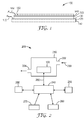
- sensor element 100 comprises dielectric 110 substrate supporting first conductive electrode 120 having an optional first conductive member 122 electrically coupled thereto.
- Absorptive dielectric layer 130 comprises a polymer of intrinsic microporosity, and is disposed between first conductive electrode 120 and second conductive electrode 140.
- Second conductive electrode 140 comprises carbon nanotubes and is permeable to at least one organic vapor.
- An ultrathin noble metal layer 180 is disposed between absorptive dielectric layer 130 and second conductive electrode 140.
- Optional second conductive member 142 is electrically coupled to second conductive electrode 140.
- Optional cover layer 150 is disposed on second conductive electrode 140.
- the first and second electrodes are generally planar, parallel, and disposed on opposite sides of the absorptive dielectric layer, although it will be recognized that other configurations are possible.
- the sensor element is configured such that the absorptive dielectric layer is in sufficiently close proximity to the first conductive electrode and the second conductive electrode that the absorptive dielectric material contained in the layer will be capable of interacting with an electric field that is established by the electrodes.
- the absorptive dielectric layer exhibits a change in an electrical property upon absorption of one or more analytes (e.g., one or more organic vapors).
- the electrical property is capacitance or a capacitance-related property as described below.
- Such a change in a capacitance-related property can be measured by imparting a charge differential between the first conductive electrode and the second conductive electrode (e.g., by imparting a voltage differential to the electrodes) and monitoring the property of the sensor element in response to the presence of the analyte.
- Such monitoring can be done by the use of an operating circuit, as described later herein.
- capacitor and “capacitance-related property” encompass any electrical property and the measurement thereof that is in general associated with the imparting of an electrical charge (whether static or time variant) and the monitoring of an electrical property during and/or after the imparting of the charge.
- Such properties include, for example, not only capacitance, but also impedance, inductance, admittance, current, resistance, and conductance, and may be measured according to various methods known in the art.
- the absorptive dielectric layer (the term “layer” being used generically and encompassing any physical configuration) comprises at least in part an absorptive dielectric material.
- absorptive dielectric material means a material that is capable of absorbing an organic chemical analyte, and that can exhibit a measurable change in some electrical property of the material upon absorbing the organic analyte into the material.
- FIG. 1 depicts a parallel plate type of configuration
- other configurations are also possible.
- a configuration wherein the first and second electrodes are interdigitated is also possible and within the scope of the present disclosure.
- the absorptive dielectric material is chosen from the family of materials comprising so-called "polymers of intrinsic microporosity” (hereafter called PIMs).
- PIMs polymers of intrinsic microporosity
- Such polymers include, but are not limited to, those disclosed in " Polymers of Intrinsic Microporosity (PIMs): Robust, Solution-Processable, Organic Microporous Materials," Budd et al., Chem. Commun., 2004, pp. 230-231 ; in “ Polymers of Intrinsic Microporosity (PIMs),” McKeown et al., Chem. Eur. J., 2005, 11, No. 9, 2610-2620 ; in US Patent Application Publication 2006/0246273 to McKeown et al. ; and in Published PCT application No. WO 2005/012397A2 to McKeown et al.
- PIMs can be formulated via the use of any combination of monomers that member to a very rigid polymer within which there are sufficient structural features to induce a contorted structure.
- PIMs can comprise organic macromolecules comprised of generally planar species connected by rigid linkers, said rigid linkers having a point of contortion such that two adjacent planar species connected by the rigid linkers are held in non-coplanar orientation.
- such materials can comprise organic macromolecules comprised of first generally planar species connected by rigid linkers predominantly to a maximum of two other said first species, said rigid linkers having a point of contortion such that two adjacent first planar species connected by the rigid linkers are held in non-coplanar orientation.
- such a point of contortion may comprise a spiro group, a bridged ring moiety or a sterically congested single covalent bond around which there is restricted rotation.
- PIMs have the advantage of possessing microporosity that is not significantly dependent on the thermal history of the material. PIMs thus may offer advantages in terms of being reproducibly manufacturable in large quantities, and in terms of not exhibiting properties that change upon aging, shelf life, etc.
- microporous and “microporosity” mean that the material has a significant amount of internal, interconnected pore volume, with the mean pore size (as characterized, for example, by sorption isotherm procedures) being less than about 100 nanometers (nm), typically less than about 10 nm.
- mean pore size as characterized, for example, by sorption isotherm procedures
- Such microporosity provides that molecules of organic analyte (if present) will be able to penetrate the internal pore volume of the material and take up residence in the internal pores.
- the presence of such analyte in the internal pores can alter the dielectric properties of the material such that a change in the dielectric constant (or any other suitable electrical property) can be observed.
- the disclosed sensor element may have advantageous properties with regard to the sensor of an organic analyte, in that a measurable change in an electrical property of the dielectric material may be caused by the presence of the analyte molecules in the pores.
- a measurable change in an electrical property of the dielectric material may be caused by the presence of the analyte molecules in the pores.
- it may be possible to detect the analyte without the analyte molecules being required to be solubilized in the polymeric material itself to a sufficient extent to cause a change in a property of the polymeric material such as swelling and/or expansion (although such a phenomenon may also occur and may also contribute to a measurable electrical response).
- Such a microporous nature of the absorptive dielectric material may contribute to increased sensitivity of the dielectric material to small amounts of organic analyte.
- the PIM comprises a porosity of at least about 10 percent, at least about 20 percent, or at least about 30 percent (as characterized, for example, by sorption isotherm techniques, such as those using instruments available under the trade designation AUTOSORB from Quantachrome Instruments of Boynton Beach, Florida).
- porosity can provide good response to low levels of organic chemical analytes.
- the material should not have such a high pore volume that it is difficult to avoid electrical shorting or arcing between the first conductive electrode and the second conductive electrode.
- the material comprises a porosity of at most about 90 percent, at most about 60 percent or at most about 40 percent.
- the size and distribution of the internal pores may be such that at least some of the organic analyte molecules in at least some of the pores may form a more highly condensed state (e.g., a quasi-liquid state) than they would otherwise be in (e.g., than they would be in the environment in which the analyte is monitored).
- a more highly condensed state e.g., a quasi-liquid state
- the analyte molecules collecting in the internal pores in larger numbers and/or at a higher concentration than they are present in the environment being monitored; in addition, or instead, the analyte molecules in this state may exhibit a higher dielectric constant (relative permittivity) than in an uncondensed vaporous or gaseous state.
- the PIM comprises an average pore size of less about 50 nm, less than about 20 nm, or less than about 10 nm. In various embodiments, the PIM comprises an average pore size of greater than about 0.3 nm, greater than about 0.5 nm, or greater than about 1.0 nm.
- the PIM is a hydrophobic material (e.g., a hydrophobic organic polymeric material), that will not absorb liquid water to an extent that the material swells significantly or otherwise exhibits a significant change in a physical property.
- a hydrophobic material e.g., a hydrophobic organic polymeric material
- Such hydrophobic properties are useful in providing an organic analyte sensor element that is relatively insensitive to the presence of water.
- the material may however comprise relatively polar moieties for specific purposes.
- the PIM comprises a continuous matrix.
- a continuous matrix is defined as an assembly (e.g., a coating, layer, etc.) in which the solid portion of the material is continuously interconnected (irrespective of the presence of porosity as described above, or of the presence of optional additives as discussed below). That is, a continuous matrix is distinguishable from an assembly that comprises an aggregation of particles (e.g., zeolites, activated carbons, carbon nanotubes, etc.).
- a layer or coating deposited from a solution will typically comprise a continuous matrix (even if the coating itself is applied in a patterned manner and/or comprises particulate additives).
- a collection of particles deposited via powder spraying, coating and drying of a dispersion (e.g., a latex), or by coating and drying of a sol-gel mixture, may not comprise a continuous network as defined by applicant. However, if such a latex, sol-gel, etc., layer can be consolidated such that individual particles are no longer discernible, nor is it possible to discern areas of the assembly that were obtained from different particles, such a layer may then meet applicant's definition of a continuous matrix.
- PIMs are soluble in common organic solvents and thus are amenable to conventional deposition processes such as coating.
- the material may be crosslinked using a suitable crosslinking agent, for example bis(benzonitrile)palladium(II) dichloride. This process may render the absorptive dielectric layer insoluble in organic solvents, and/or may enhance certain physical properties such as durability, abrasion resistance, etc., which may be desirable in certain applications.
- a suitable crosslinking agent for example bis(benzonitrile)palladium(II) dichloride.
- the PIMs may be blended with other materials.
- the PIM may be blended with a material that itself is not an absorptive dielectric material. Even though not contributing to an analyte response, such a material may be useful for other reasons. For example, such a material may allow the formation of a PIM-containing layer which has superior mechanical properties and the like.
- PIMs may be dissolved in a common solvent with the other material to form a homogeneous solution, which may be cast to form an absorptive dielectric blend layer comprising both the PIM and the other polymer(s).
- PIMs may also be blended with a material that is an absorptive dielectric material (for example, zeolites, activated carbon, silica gel, hyper-crosslinked polymer networks and the like).
- a material that is an absorptive dielectric material for example, zeolites, activated carbon, silica gel, hyper-crosslinked polymer networks and the like.
- Such materials may comprise insoluble materials that are suspended in a solution comprising of a PIMs material. Coating and drying of such a solution/suspension may provide a composite absorptive dielectric layer comprising both the PIM material and the additional absorptive dielectric material.
- the absorptive dielectric material may have any thickness, but typically is in a range of from about 100 to 3000 nanometers (nm). More typically, the absorptive dielectric material forms a layer having a thickness in a range of from 300 nm to 1000 nm, or even from 400 to 800 nm.
- the absorptive layer may contain additives such as fillers, antioxidants, light stabilizers in addition to the PIM material, but since they may tend to interfere with proper operation of the sensor element such additives are typically minimized or not present. Combinations of PIM materials may be used.
- an additional layer or layers of material that is not an absorptive dielectric material may be provided in proximity to the absorptive dielectric layer.
- a layer or layers may be provided for any of a variety of reasons; for example, as a protective layer or as a tie layer to improve adhesion.
- multiple individual layers of absorptive dielectric material can be used.
- multiple layers of PIM materials can be used.
- one or more layers of some other absorptive dielectric material can be used in addition to a layer of PIM material.
- the various layers of absorptive dielectric material can be in direct contact with each other; or, they can be separated by a layer or layers present for some other purpose (e.g., passivation layers, tie layers, as described herein).
- the first conductive electrode can comprise any suitable conductive material. Combinations of different materials (conductive and/or nonconductive) can be used, as different layers or as a mixture, as long as sufficient overall conductivity is provided, Typically, the first conductive electrode has a sheet resistance of less than about 10 7 ohms/square. Examples of materials that can be used to make the first conductive electrode and/or second conductive electrode include, but are not limited to, organic materials, inorganic materials, metals, alloys, and various mixtures and composites comprising any or all of these materials. In certain embodiments, coated (for example, thermal vapor coated, sputter coated, etc.) metals or metal oxides, or combinations thereof, may be used. Suitable conductive materials include for example aluminum, nickel, titanium, tin, indium-tin oxide, gold, silver, platinum, palladium, copper, chromium, and combinations thereof.
- the first conductive electrode can be of any thickness as long as it is conductive; for example, in a thickness in a range of from at least 4 nm to 400 nm, or from 10 nm to 200 nm. If the first conductive electrode is thicker than about 1000 nm or greater, it can become difficult for the second conductive electrode to bridge the edge of the electrode to make a conductive path. If the first conductive electrode is too thick, then the edge of the first conductive electrode may be sloped so that the second conductive electrode can make a continuous conductive path.
- the second conductive electrode comprises carbon nanotubes.
- Useful carbon nanotubes include single-walled carbon nanotubes and multi-walled carbon nanotubes.
- the second conductive electrode may have a carbon nanotubes content of at least 50, 60, 70, 80, 90, 95, 99, or even at least 99.9 percent by weight.
- the second conductive electrode consists of, or consists essentially of, multi-walled carbon nanotubes.
- the second layer may include additional components as long as it remains permeable to at least one organic analyte. Combinations of different materials (conductive and/or nonconductive) can be used, as different layers or as a mixture, as long as sufficient overall conductivity and permeability is provided.
- the second conductive electrode has a sheet resistance of less than about 10 7 ohms/square.
- the second conductive electrode typically has a thickness in a range of from 0.1 to 100 micrometers, although other thicknesses may be used.
- the second conductive electrode may have a thickness in a range of from 0.1 to 10 micrometers, or from 1 to 5 micrometers. Greater thicknesses may have undesirably low levels of permeability, while lesser thicknesses may become insufficiently conductive and/or difficult to electrically connect to the second conductive member. Since the second conductive electrode is permeable, the first electrode typically comprises a continuous, uninterrupted layer, but it may contain openings or other interruptions if desired.
- the second conductive electrode can be prepared by any suitable technique such as, for example, solution/dispersion coating techniques (e.g., dip coating, spin coating, or flood coating).
- a surfactant may be used in conjunction with solutions/dispersions of the carbon nanotubes to enhance wetting of the absorptive layer.
- An ultra-thin ( ⁇ 1 nanometer thick) layer of a noble metal such as, for example, gold, platinum, or palladium, or a combination thereof, is deposited on the absorptive layer prior to coating with the carbon nanotubes to facilitate wetting of the absorptive layer.
- a dielectric substrate (which may be a continuous slab, layer or film of material) that is in proximity to the first electrode and that may serve to provide physical strength and integrity to the finished sensor element. Any suitable material may be used, including glass, ceramic, plastic, etc. In large scale production, a polymeric film (such as polyester) may be used. In some embodiments, the dielectric substrate is an analyte-permeable material (e.g., silicone rubber or a microporous membrane).
- the first conductive electrode is provided on the dielectric substrate.
- the conductive layer may comprise any of the materials mentioned above, including blends or mixtures of conductive and nonconductive materials, and may be deposited by any suitable method, including but not limited to spin coating, dip coating, screen printing, transfer coating, sputter-coating, physical vapor deposition, chemical vapor deposition, or a combination of two or more of such methods.
- the conductive layer may be provided by placing a premade film (e.g., a metal foil or conductive tape) atop the dielectric substrate. This first conductive electrode may be provided as a continuous layer or as a discontinuous layer, as previously described.
- the first conductive electrode is provided such that the first conductive electrode is in proximity to, and/or in contact with, at least a portion of the dielectric substrate.
- an optional layer is present between at least a portion of the first conductive electrode, and the dielectric substrate. Such an optional layer may be used for any purpose (e.g., such as improving the bond between first conductive electrode and the dielectric substrate), as long as the layer does not interfere with the functioning of the sensor element.
- the first and second conductive members may be electrically coupled to the first and second conductive electrodes at any appropriate point during assembly of the sensor element.
- the first conductive member may be attached to the first conductive electrode immediately after deposition of the first conductive electrode and before deposition of the absorptive dielectric layer.
- the absorptive dielectric layer may be deposited on the first conductive electrode such that an area of the first conductive electrode is left exposed for attachment to the first conductive member.
- the second conductive member may be attached to the second conductive electrode immediately after deposition of the second conductive electrode and before deposition of the optional cover layer, or the optional cover layer may be deposited on the second conductive electrode such that an area of the second conductive electrode is left exposed for attachment to the second conductive member.
- the absorptive dielectric material is placed in proximity to the first conductive electrode by a coating process; for example, including but not limited to solvent coating, spin coating, dip coating, transfer coating, screen printing, and the like.
- the dielectric material is deposited in such a manner as to minimize the presence of defects, pinholes, etc., that might serve to compromise the performance of the sensor element.
- the absorptive dielectric layer comprises a polymer of intrinsic microporosity that is deposited by coating a solution of PIM material upon a suitable dielectric substrate and allowing the solution to dry so as to form a solid layer comprising the PIM material.
- An absorptive dielectric layer can also be provided by other methods.
- a preformed film of absorptive dielectric material can be placed upon the second surface of the first conductive electrode.
- the absorptive dielectric material can be provided in particulate form (e.g., as a powder, as a suspension, or as a sol) and deposited in such a form onto a first conductive electrode so as to form a particulate coating. If desired, such a material can be consolidated so as to form a continuous matrix of absorptive dielectric material.
- An optional protective cover or barrier layer can be provided in proximity to at least one of the first or second conductive electrodes.
- a cover layer can be placed atop the second conductive electrode, leaving an area of second conductive electrode accessible for electrical contact with the second conductive member electrical contact. Any such cover layer should not significantly interfere with the functioning of sensor element. For example, if the sensor element is configured such that an analyte of interest must pass through cover layer in order to reach the absorptive dielectric layer, the cover layer should be sufficiently permeable to the analyte.
- the optional cover layer may be deposited by any method known in the art, including coating (e.g., spin coating, dip coating, solvent coating, vapor coating, transfer coating, screen printing, flexographic printing, and the like).
- the cover layer can comprise a premade layer (e.g., a film or tape) that is placed upon the second conductive electrode.
- the cover layer is provided such that the cover layer is in direct contact with at least a portion of a major surface of the second conductive electrode.
- the cover layer may be the outermost layer of the sensor element, or may itself receive additional coatings or layers if desired.
- the first conductive electrode and the absorptive dielectric layer are in direct contact, with no interposing layer(s) therebetween.
- the second conductive electrode and the absorptive dielectric layer are in direct contact, with no interposing layer(s) therebetween.
- Such embodiments are pictured in Fig. 1 .
- other, optional layers may be present between the first conductive electrode and the absorptive dielectric layer, and/or between the second conductive electrode and the absorptive dielectric layer. In such a case, either or both of the electrodes may not be in direct contact with some or all of a surface of the absorptive dielectric material.
- a tie layer or layers may be used to improve the bonding between an electrode and the absorptive dielectric layer.
- a passivation layer or layers for example, a layer of silicon dioxide
- a single layer may serve multiple functions.
- Any such optional layer or layers such as the aforementioned tie layers, passivation layers, protective layers, cover layers, etc., may be used, for whatever purpose, as long as they do not significantly interfere with the desired functioning of the sensor element.
- an optional layer should be sufficiently permeable to an analyte of interest if the sensor element is configured such that the analyte must pass through the optional layer in order to reach the absorptive dielectric layer.
- edges of the first and/or second electrodes and/or absorptive dielectric layer can be aligned flush with each other, or, they may be recessed and/or extended relative to each other or any other layers that may be present.
- an electrically accessible area may be provided on the first conductive electrode to enable electrical contact between the electrode and an operating circuit.
- an electrically accessible area may be similarly provided.
- Such electrically accessible areas can be provided in any convenient location.
- a connecting device e.g., a contact pad, tab, or the like
- a connecting device may be placed in electrical contact with accessible area of first conductive electrode.
- a connecting device may be placed likewise in contact with an accessible area of the second conductive electrode.
- a detectable change in an electrical property associated with the sensor element may occur.
- Such a detectable change may be detected by an operating circuit that is in electrical communication with the first and second conductive electrodes.
- "operating circuit” refers generally to an electrical apparatus that can be used to apply a voltage to the first conductive electrode and the second conductive electrode (thus imparting a charge differential to the electrodes), and/or to monitor an electrical property of the sensor element, wherein the electrical property may change in response to the presence of an organic analyte.
- the operating circuit may monitor any or a combination of inductance, capacitance, voltage, resistance, conductance, current, impedance, phase angle, loss factor, or dissipation.
- Such an operating circuit may comprise a single apparatus which both applies voltage to the electrodes, and monitors an electrical property.
- such an operating circuit may comprise two separate apparatuses, one to provide voltage, and one to monitor the signal.
- the operating circuit is typically electrically coupled to first conductive electrode and to second conductive electrode by conductive members.
- exemplary sensor device 200 includes a sensor chamber 210 having an inlet opening 222 and optional outlet opening 224.
- Sensor element 100 (as described hereinabove) is disposed within the sensor chamber 210, and is in fluid communication with the inlet opening 222 and optional outlet opening 224, if present.
- a sample containing analyte 230 enters sensing chamber 210, where it contacts sensor element 100.
- An operating circuit 240 is in electrical communication via conductive pathways 290 with sensor element 100. When connected to a source of electrical power 270, operating circuit 240 measures the capacitance of sensor element 100.
- operating circuit 240 is communicatively coupled to data storage device 250, controller device 280, and/or display device 260.
- the operating circuit 240 is in electrical communication with a source of electrical power 270.
- Exemplary sources of electrical power include batteries, plug in power supplies, generators, hardwired power supplies, and RF generators (if the operating circuit includes an RF receiver).
- the sensor chamber can be constructed of any solid material that is impermeable to the analyte. Examples include metal and/or plastic.
- Exemplary display devices 260 include LED displays, LCD displays, CRT displays, galvanic meters, and printers. Controller device 280, if present, includes hardware and/or software that directs operation of the operating circuit.
- Exemplary data storage devices 250 include flash memory cards, hard disks, digital tape, and CD R media.
- the operating circuit may be provided in direct contact with the first and/or the second conductive electrode, either via connecting members, or by contacting some portion of the operating circuit directly to an electrically accessible area of each electrode.
- an operating circuit can be provided that resides on a circuit board or a flexible circuit (either of which can also serve as the dielectric substrate).
- the first conductive electrode can then be deposited directly onto the dielectric substrate such that it is in direct contact with a portion of the operating circuit.
- Sensor elements and sensor devices can be used to detect and/or monitor (whether qualitatively or quantitatively) the presence of an organic analyte or analytes.
- analytes can include, but are not limited to, hydrocarbons, fluorocarbons, alkanes, cycloalkanes, aromatic compounds, alcohols, ethers, esters, ketones, halocarbons, amines, organic acids, cyanates, nitrates, and nitriles, for example n-octane, cyclohexane, methyl ethyl ketone, acetone, ethyl acetate, carbon disulfide, carbon tetrachloride, benzene, styrene, toluene, xylenes, methyl chloroform, tetrahydrofuran, methanol, ethanol, isopropyl alcohol, n-butyl alcohol, t-butyl alcohol, 2-e
- Organic analytes can be relatively nonpolar organic molecules or relatively polar organic molecules.
- Analytes are typically vapors; that is, molecules that are capable of condensing to form a solid or liquid under the ambient conditions of temperature and pressure that the analyte is experiencing (e.g., toluene, acetone, or heptane).
- the present disclosure provides a sensor element as defined in claim 1.
- the present disclosure provides a sensor element according to the first embodiment, further comprising a dielectric substrate supporting the first conductive electrode.
- the present disclosure provides a sensor element according to the second embodiment, wherein the dielectric substrate comprises a polymeric film.
- the present disclosure provides a sensor element according to any one of the first to third embodiments, wherein the carbon nanotubes comprise at least 99 percent by weight of the second conductive electrode.
- the present disclosure provides a sensor element according to any one of the first to fourth embodiments, wherein the carbon nanotubes comprise multi-walled carbon nanotubes.
- the present disclosure provides a sensor element according to any one of the first to fifth embodiments, wherein the polymer of intrinsic microporosity comprises organic macromolecules comprised of generally planar species connected by rigid linkers, said rigid linkers having a point of contortion such that two adjacent planar species connected by one of the rigid linkers are held in non-coplanar orientation.
- the present disclosure provides a sensor element according to any one of the first to sixth embodiments, wherein the first conductive electrode comprises carbon nanotubes and is permeable to at least one organic vapor.
- the present disclosure provides a sensor element according to any one of the first to seventh embodiments, wherein the second conductive electrode is coextensive with a major surface of the absorptive dielectric layer.
- the present disclosure provides a method as defined in claim 7.
- the present disclosure provides a method according to the ninth embodiment, wherein the first conductive electrode is supported on a dielectric substrate.
- the present disclosure provides a method according to the tenth embodiment, wherein the dielectric substrate comprises a polymeric film.
- the present disclosure provides a method according to any one of the ninth to eleventh embodiments, wherein the steps are sequential.
- the present disclosure provides a method according to any one of the ninth to twelfth embodiments, wherein the carbon nanotubes comprise at least 99 percent by weight of the second conductive electrode.
- the present disclosure provides a method according to any one of the ninth to thirteenth embodiments, wherein the carbon nanotubes comprise multi-walled carbon nanotubes.
- the present disclosure provides a method according to any one of the ninth to fourteenth embodiments, wherein the polymer of intrinsic microporosity comprises organic macromolecules comprised of generally planar species connected by rigid linkers, said rigid linkers having a point of contortion such that two adjacent planar species connected by the rigid linkers are held in non-coplanar orientation.
- the present disclosure provides a method according to any one of the ninth to fifteenth embodiments, wherein the first conductive electrode comprises carbon nanotubes and is permeable to at least one organic vapor.
- the present disclosure provides a method according to any one of the ninth to sixteenth embodiments, wherein the second conductive electrode is coextensive with a major surface of the absorptive dielectric layer.
- the present disclosure provides a sensor device as defined in claim 13.
- the present disclosure provides a sensor device according to the eighteenth embodiment, wherein the sensor chamber further comprises an outlet opening in fluid communication with the inlet opening.
- the present disclosure provides a sensor device according to the eighteenth or nineteenth embodiment, further comprising a display device in communicatively coupled with the operating circuit.
- the present disclosure provides a sensor device according to any one of the eighteenth to twentieth embodiments, wherein the carbon nanotubes comprise multi-walled carbon nanotubes.
- the titanium bottom electrode corresponds to a first conductive electrode
- the top MWCNT electrode is equivalent to a second conductive electrode
- PIM Polymer of Intrinsic Microporosity
- Schott glass was cut into 5.1-cm (2-inch) squares using a standard glass cutting tool.
- the Schott glass was prepared for vapor coating by sonicating it for 30 minutes at 50°C using a Branson Model 1510 sonicator (from Branson Ultrasonics Corporation of Danbury, Connecticut) with Alconox Liqui-Nox detergent, rinsing it well with hot tap water then deionized water (DI water), allowing it to drain, then oven drying it for 30 minutes at 65°C. This produced glass that was visually clean.
- a Branson Model 1510 sonicator from Branson Ultrasonics Corporation of Danbury, Connecticut
- DI water deionized water
- the glass substrate was masked with a thin strip approximately 2 mm wide of removable tape to isolate upper and lower electrode regions. This strip was placed roughly 1.8 cm from the bottom edge.
- a titanium bottom electrode was prepared by vapor depositing 100.0 nanometers of titanium onto the glass substrate at a rate of 0.5 nm/sec. A small margin around the border of the glass was blocked by the sample holder from the titanium coating. The removable tape was removed after vapor deposition. This produced an electrode having two regions covered with titanium: an upper region that was about 3 cm x 5 cm and a lower region that was about 1.8 cm x 5 cm. The small margin around the glass was not covered with titanium and there was a gap of about 2 mm between the two electrode regions which was protected from the titanium vapor deposition by the Removable Tape.
- a 4.5 percent by weight solution of PIMS was prepared in chlorobenzene by mixing the components in a small jar and placing it on a roller mill (MINI BOTTLE ROLLER, number 348920, from Wheaton Science Products of Millville, New Jersey) overnight to complete dissolution.
- the solution was filtered through a one-micrometer filter (ACRODISC 25 MM SYRINGE FILTER WITH 1 MICRON GLASS FIBER MEMBRANE from PALL Life Sciences of Ann Arbor, Michigan) prior to spin coating.
- the spin coating conditions were: one minute at 1200 rpm using a Model WS 400B-8NPP/LITE spin coater from Laurell Technologies Corporation of North Wales, Pennsylvania.
- the lower portion of the electrode was masked with the Removable Tape to prevent it from being overcoated with PIMS.
- the titanium substrate was placed in the spin coater and about one ml of chlorobenzene was applied to clean off the surface. Then approximately 0.5 ml of the PIMS/chlorobenzene solution was applied.
- the thickness was measured using a Model XP-1 Profilometer from AMBiOS Technology of Santa Cruz, California. The parameters used in the thickness measurement were a scan speed of 0.1 mm/sec, a scan length of 5 mm, a range of 10 microns, a stylus force of 0.20 mg and a filter level of 4.
- the thickness of the coating was between 500 and 600 nm on average.
- the sample was then placed in an oven at 100°C for one hour to complete the drying process.
- the resulting sample had PIMS coated over approximately the top 3 cm of the substrate with the vapor deposited titanium exposed on the bottom 1.8 cm of the substrate.
- MWCNTs Multiwalled Carbon Nanotubes
- MWCNTs were purified as follows: They were first refluxed by 3 M HNO 3 for 4 hours, rinsed by DI water, filtered by a paper filter (WHATMAN FILTER PAPER GRADE 1 available from Whatman Inc. of Piscataway, New Jersey), then dried at 80°C to reduce metal catalysts. The dried MWCNTs were then put through an air burning process (480°C furnace for 30 minutes) to remove amorphous carbons. The remaining material was then put through the HNO 3 reflux process (reflux by 3 M HNO 3 followed by rinsing with DI water, filtration and drying at 80°C) again for one hour.
- HNO 3 reflux process reflux by 3 M HNO 3 followed by rinsing with DI water, filtration and drying at 80°C again for one hour.
- Purified MWCNTs were added to a one percent by weight solution of Triton X-100 in DI water solution via ultrasonic agitation (using Ultrasonic Cleaner Model 3510 from Branson Ultrasonics Corporation, Danbury, Connecticut) followed by centrifugal separation (using MODEL IEC CENTRA CL2 from Thermo Fisher Scientific Inc. of Waltham, Massachusetts) and decantation resulting in a stable one percent by weight dispersion of MWCNTs.
- the dispersion of the MWCNTs was applied to the PIMS coated surface by knife coating (using a GARDCO MICROM II KNIFE COATER, available from the Paul N. Gardner Company, Inc. of Pompano Beach, Florida).
- the knife coater setting was adjusted with the two micrometer dials on the ends of the knife coater. The micrometers were zeroed after placing the knife coater on a flat surface with the knife blade just touching the surface.
- the knife coater setting was then fixed by adjusting the micrometers to a setting of 6.5 on the smallest scale of the micrometers. This gave a gap between the knife blade and the substrate of about 0.16 mm.
- the sample was baked at 125°C in a N 2 environment for 13 minutes, followed by DI water rinsing to remove surfactant that was used in forming the MWCNT electrode.
- the coating was rebaked for over 10 minutes to complete the drying of the coating.
- the resistance of the MWCNT coating was about 6-8 k ⁇ from edge to edge of the MWCNT coating ( ⁇ 5 cm) after DI water rinsing and drying.
- portions of the top MWCNT layer were removed to leave an approximately 14 mm x 14 mm active sensor area over part of the upper region of the substrate (the approximately 3.0 cm x 5 cm titanium coated region) with the MWCNT extending over the vapor deposited titanium covering the lower region of the substrate (the approximately 1.8 cm x 5 cm titanium coated region).
- the top electrode of the sensor was the MWCNT layer which was in direct electrical contact with the approximately 1.8 cm x 5 cm titanium coated region of the substrate.
- the bottom electrode of the sensor was the approximately 3.0 cm x 5 cm titanium coated region of the substrate.
- Capacitance measurements were made on an LCR meter (INSTEK MODEL LCR-821 HIGH PRECISION LCR METER from Good Will Instruments, Co., Ltd. of Taipei, Taiwan) applying one volt at 1000 Hz across the top and bottom electrodes. Contact to the bottom and top electrodes of the sensor were made by attaching alligator clips to exposed titanium along the side of the sensor.
Landscapes
- Chemical & Material Sciences (AREA)
- Health & Medical Sciences (AREA)
- General Health & Medical Sciences (AREA)
- Life Sciences & Earth Sciences (AREA)
- Engineering & Computer Science (AREA)
- Analytical Chemistry (AREA)
- Physics & Mathematics (AREA)
- Electrochemistry (AREA)
- Chemical Kinetics & Catalysis (AREA)
- Biochemistry (AREA)
- General Physics & Mathematics (AREA)
- Immunology (AREA)
- Pathology (AREA)
- Nanotechnology (AREA)
- Power Engineering (AREA)
- Molecular Biology (AREA)
- Crystallography & Structural Chemistry (AREA)
- Investigating Or Analyzing Materials By The Use Of Electric Means (AREA)
Applications Claiming Priority (2)
| Application Number | Priority Date | Filing Date | Title |
|---|---|---|---|
| US38813010P | 2010-09-30 | 2010-09-30 | |
| PCT/US2011/049145 WO2012044419A1 (en) | 2010-09-30 | 2011-08-25 | Sensor element, method of making the same, and sensor device including the same |
Publications (2)
| Publication Number | Publication Date |
|---|---|
| EP2622334A1 EP2622334A1 (en) | 2013-08-07 |
| EP2622334B1 true EP2622334B1 (en) | 2016-05-25 |
Family
ID=44681415
Family Applications (1)
| Application Number | Title | Priority Date | Filing Date |
|---|---|---|---|
| EP11761429.7A Not-in-force EP2622334B1 (en) | 2010-09-30 | 2011-08-25 | Sensor element, method of making the same, and sensor device including the same |
Country Status (5)
| Country | Link |
|---|---|
| US (1) | US9341588B2 (ja) |
| EP (1) | EP2622334B1 (ja) |
| JP (1) | JP5932806B2 (ja) |
| CN (1) | CN103154714A (ja) |
| WO (1) | WO2012044419A1 (ja) |
Cited By (1)
| Publication number | Priority date | Publication date | Assignee | Title |
|---|---|---|---|---|
| WO2018234896A1 (en) * | 2017-06-20 | 2018-12-27 | Abdolahad Mohammad | REAL-TIME AND MARKER-FREE ANALYZER FOR IN VITRO AND IN VIVO DETECTION OF SUSPECTED REGIONS IN CANCER |
Families Citing this family (30)
| Publication number | Priority date | Publication date | Assignee | Title |
|---|---|---|---|---|
| EP2174360A4 (en) | 2007-06-29 | 2013-12-11 | Artificial Muscle Inc | CONVERTER WITH ELECTROACTIVE POLYMER FOR SENSOR REVIEW APPLICATIONS |
| EP2239793A1 (de) | 2009-04-11 | 2010-10-13 | Bayer MaterialScience AG | Elektrisch schaltbarer Polymerfilmaufbau und dessen Verwendung |
| WO2012050686A1 (en) | 2010-09-30 | 2012-04-19 | 3M Innovative Properties Company | Sensor element, method of making the same, and sensor device including the same |
| WO2012118916A2 (en) | 2011-03-01 | 2012-09-07 | Bayer Materialscience Ag | Automated manufacturing processes for producing deformable polymer devices and films |
| WO2012129357A2 (en) | 2011-03-22 | 2012-09-27 | Bayer Materialscience Ag | Electroactive polymer actuator lenticular system |
| WO2012141925A1 (en) | 2011-04-13 | 2012-10-18 | 3M Innovative Properties Company | Method of detecting volatile organic compounds |
| US9279792B2 (en) | 2011-04-13 | 2016-03-08 | 3M Innovative Properties Company | Method of using an absorptive sensor element |
| US9506888B2 (en) | 2011-04-13 | 2016-11-29 | 3M Innovative Properties Company | Vapor sensor including sensor element with integral heating |
| EP2718706B1 (en) | 2011-06-08 | 2015-03-11 | 3M Innovative Properties Company | Humidity sensor and sensor element therefor |
| WO2012174099A1 (en) | 2011-06-16 | 2012-12-20 | 3M Innovative Properties Company | Surface plasmon resonance sensor element and sensor including the same |
| CN104024848B (zh) | 2011-12-13 | 2016-01-20 | 3M创新有限公司 | 用于识别和定量测定气体介质中的未知有机化合物的方法 |
| US9876160B2 (en) | 2012-03-21 | 2018-01-23 | Parker-Hannifin Corporation | Roll-to-roll manufacturing processes for producing self-healing electroactive polymer devices |
| WO2013180936A1 (en) | 2012-05-29 | 2013-12-05 | 3M Innovative Properties Company | Humidity sensor and sensor element |
| KR20150031285A (ko) | 2012-06-18 | 2015-03-23 | 바이엘 인텔렉쳐 프로퍼티 게엠베하 | 연신 공정을 위한 연신 프레임 |
| EP2864770B1 (en) | 2012-06-25 | 2017-09-27 | 3M Innovative Properties Company | Sensor element, method of making, and method of using the same |
| JP6263179B2 (ja) | 2012-08-02 | 2018-01-17 | スリーエム イノベイティブ プロパティズ カンパニー | 携帯用電子装置及び蒸気センサカード |
| US9317068B2 (en) | 2012-09-24 | 2016-04-19 | Donaldson Company, Inc. | Venting assembly and microporous membrane composite |
| TW201436311A (zh) * | 2012-10-16 | 2014-09-16 | 拜耳智慧財產有限公司 | 金屬化介電膜之方法 |
| WO2014066576A1 (en) | 2012-10-24 | 2014-05-01 | Bayer Intellectual Property Gmbh | Polymer diode |
| CN105578969B (zh) * | 2013-09-26 | 2019-01-22 | 3M创新有限公司 | 适用于检测在皮肤部位处的醇残留的蒸汽传感器 |
| CN103698360A (zh) * | 2013-12-13 | 2014-04-02 | 苏州纳格光电科技有限公司 | 半导体气体传感器 |
| KR102414098B1 (ko) * | 2014-02-27 | 2022-06-29 | 쓰리엠 이노베이티브 프로퍼티즈 캄파니 | 주변-미만 온도 증기 센서 및 이용 방법 |
| SG10201900469PA (en) | 2014-07-22 | 2019-02-27 | Brewer Science Inc | Thin-film resistive-based sensor |
| EP3232905B1 (en) * | 2014-12-18 | 2021-02-17 | Koninklijke Philips N.V. | Hydration state indicator |
| US10083883B2 (en) * | 2016-06-20 | 2018-09-25 | Applied Materials, Inc. | Wafer processing equipment having capacitive micro sensors |
| WO2018047936A1 (ja) * | 2016-09-09 | 2018-03-15 | 北陸電気工業株式会社 | 容量型ガスセンサ |
| US10209186B2 (en) * | 2017-01-03 | 2019-02-19 | International Business Machines Corporation | Chemical sensing based on plasmon resonance in carbon nanotubes |
| EP3762391A4 (en) | 2018-03-08 | 2022-08-03 | ExxonMobil Technology and Engineering Company | SPIROCENTRIC COMPOUNDS AND POLYMERS THEREOF |
| WO2020036171A1 (ja) * | 2018-08-17 | 2020-02-20 | 富士フイルム株式会社 | センサ |
| CN109546890B (zh) * | 2019-01-18 | 2020-07-31 | 清华大学 | 湿气发电方法及装置 |
Citations (2)
| Publication number | Priority date | Publication date | Assignee | Title |
|---|---|---|---|---|
| US20050045493A1 (en) * | 2003-08-29 | 2005-03-03 | Mahurin Shannon Mark | Method and apparatus for detection of chemical vapors |
| US20060237310A1 (en) * | 2005-04-26 | 2006-10-26 | Patel Sanjay V | Interdigitated chemical sensors, and methods of making and using the same |
Family Cites Families (27)
| Publication number | Priority date | Publication date | Assignee | Title |
|---|---|---|---|---|
| SE9704329D0 (sv) * | 1997-11-25 | 1997-11-25 | Siemens Elema Ab | Gasmätare |
| US6085576A (en) * | 1998-03-20 | 2000-07-11 | Cyrano Sciences, Inc. | Handheld sensing apparatus |
| JP2003227806A (ja) | 2002-02-01 | 2003-08-15 | Kansai Research Institute | 気体物質検知方法 |
| US20070048180A1 (en) | 2002-09-05 | 2007-03-01 | Gabriel Jean-Christophe P | Nanoelectronic breath analyzer and asthma monitor |
| US7449146B2 (en) | 2002-09-30 | 2008-11-11 | 3M Innovative Properties Company | Colorimetric sensor |
| GB0317557D0 (en) | 2003-07-26 | 2003-08-27 | Univ Manchester | Microporous polymer material |
| GB0322832D0 (en) | 2003-09-30 | 2003-10-29 | Epigem Ltd | Sensor platforms utilising nanoporous membranes |
| US6997039B2 (en) | 2004-02-24 | 2006-02-14 | Clemson University | Carbon nanotube based resonant-circuit sensor |
| EP1730490B1 (en) * | 2004-03-31 | 2013-02-27 | Agency for Science, Technology and Research | A sensor for measuring gas permeability of a test material |
| US8052932B2 (en) * | 2006-12-22 | 2011-11-08 | Research Triangle Institute | Polymer nanofiber-based electronic nose |
| US7776269B2 (en) * | 2005-03-15 | 2010-08-17 | The United States Of America As Represented By The Secretary Of The Navy | Capacitive based sensing of molecular adsorbates on the surface of single wall nanotubes |
| US7208327B2 (en) * | 2005-05-25 | 2007-04-24 | Intel Corporation | Metal oxide sensors and method of forming |
| US7556774B2 (en) | 2005-12-21 | 2009-07-07 | 3M Innovative Properties Company | Optochemical sensor and method of making the same |
| US8293340B2 (en) | 2005-12-21 | 2012-10-23 | 3M Innovative Properties Company | Plasma deposited microporous analyte detection layer |
| US7767143B2 (en) | 2006-06-27 | 2010-08-03 | 3M Innovative Properties Company | Colorimetric sensors |
| US8067110B2 (en) | 2006-09-11 | 2011-11-29 | 3M Innovative Properties Company | Organic vapor sorbent protective device with thin-film indicator |
| CN101689607A (zh) | 2007-06-28 | 2010-03-31 | 3M创新有限公司 | 结合界面导电簇的薄膜晶体管 |
| US20090091337A1 (en) | 2007-10-04 | 2009-04-09 | Robinson Joshua A | Carbon film composite, method of manufacturing a carbon film composite and sensor made therewith |
| BRPI0816493A2 (pt) | 2007-10-05 | 2019-02-26 | 3M Innovatie Properties Company | sensor e método para detectar um analito químico orgânico e métodos de fabricação de um elemento de detecção de analito químico orgânico |
| WO2009045733A2 (en) | 2007-10-05 | 2009-04-09 | 3M Innovative Properties Company | Organic chemical sensor comprising microporous polymer, and method of use |
| JP5128380B2 (ja) * | 2008-06-19 | 2013-01-23 | 一般財団法人電力中央研究所 | 分解ガスセンサ |
| JP5662945B2 (ja) | 2008-12-23 | 2015-02-04 | スリーエム イノベイティブ プロパティズ カンパニー | 微多孔性有機ケイ酸塩材料を有する有機化学センサ |
| CN101811658B (zh) | 2009-02-20 | 2012-09-19 | 清华大学 | 碳纳米管阵列传感器及其制备方法 |
| AU2010235022B2 (en) | 2009-03-30 | 2013-08-22 | 3M Innovative Properties Company | Optoelectronic methods and devices for detection of analytes |
| EP2583090B1 (en) | 2010-06-15 | 2016-04-06 | 3M Innovative Properties Company | Variable capacitance sensors and methods of making the same |
| WO2012050686A1 (en) | 2010-09-30 | 2012-04-19 | 3M Innovative Properties Company | Sensor element, method of making the same, and sensor device including the same |
| WO2012141925A1 (en) | 2011-04-13 | 2012-10-18 | 3M Innovative Properties Company | Method of detecting volatile organic compounds |
-
2011
- 2011-08-25 CN CN2011800475842A patent/CN103154714A/zh active Pending
- 2011-08-25 JP JP2013531587A patent/JP5932806B2/ja not_active Expired - Fee Related
- 2011-08-25 WO PCT/US2011/049145 patent/WO2012044419A1/en active Application Filing
- 2011-08-25 EP EP11761429.7A patent/EP2622334B1/en not_active Not-in-force
- 2011-08-25 US US13/825,663 patent/US9341588B2/en active Active
Patent Citations (2)
| Publication number | Priority date | Publication date | Assignee | Title |
|---|---|---|---|---|
| US20050045493A1 (en) * | 2003-08-29 | 2005-03-03 | Mahurin Shannon Mark | Method and apparatus for detection of chemical vapors |
| US20060237310A1 (en) * | 2005-04-26 | 2006-10-26 | Patel Sanjay V | Interdigitated chemical sensors, and methods of making and using the same |
Cited By (1)
| Publication number | Priority date | Publication date | Assignee | Title |
|---|---|---|---|---|
| WO2018234896A1 (en) * | 2017-06-20 | 2018-12-27 | Abdolahad Mohammad | REAL-TIME AND MARKER-FREE ANALYZER FOR IN VITRO AND IN VIVO DETECTION OF SUSPECTED REGIONS IN CANCER |
Also Published As
| Publication number | Publication date |
|---|---|
| CN103154714A (zh) | 2013-06-12 |
| WO2012044419A1 (en) | 2012-04-05 |
| JP2013539040A (ja) | 2013-10-17 |
| US20130186177A1 (en) | 2013-07-25 |
| JP5932806B2 (ja) | 2016-06-08 |
| EP2622334A1 (en) | 2013-08-07 |
| US9341588B2 (en) | 2016-05-17 |
Similar Documents
| Publication | Publication Date | Title |
|---|---|---|
| EP2622334B1 (en) | Sensor element, method of making the same, and sensor device including the same | |
| EP2622333B1 (en) | Sensor element, method of making the same, and sensor device including the same | |
| EP2205965B1 (en) | Organic chemical sensor comprising microporous polymer, and method of use | |
| US10809215B2 (en) | Molecularly imprinted polymer sensors | |
| US10161896B2 (en) | Sub-ambient temperature vapor sensor and method of use | |
| EP2864770B1 (en) | Sensor element, method of making, and method of using the same | |
| US8409511B2 (en) | Organic chemical sensor with microporous organisilicate material | |
| EP2791667B1 (en) | Method for identification and quantitative determination of an unknown organic compound in a gaseous medium | |
| EP2583090B1 (en) | Variable capacitance sensors and methods of making the same | |
| EP1693667B1 (en) | Gas sensor | |
| EP2697637B1 (en) | Vapor sensor including sensor element with integral heating | |
| WO2012141883A1 (en) | Method of using an absorptive sensor element | |
| KR100856577B1 (ko) | 탄소나노튜브 센서 및 그 제조방법 | |
| US11287395B2 (en) | Capacitive gas sensor |
Legal Events
| Date | Code | Title | Description |
|---|---|---|---|
| PUAI | Public reference made under article 153(3) epc to a published international application that has entered the european phase |
Free format text: ORIGINAL CODE: 0009012 |
|
| 17P | Request for examination filed |
Effective date: 20130320 |
|
| AK | Designated contracting states |
Kind code of ref document: A1 Designated state(s): AL AT BE BG CH CY CZ DE DK EE ES FI FR GB GR HR HU IE IS IT LI LT LU LV MC MK MT NL NO PL PT RO RS SE SI SK SM TR |
|
| DAX | Request for extension of the european patent (deleted) | ||
| 17Q | First examination report despatched |
Effective date: 20140715 |
|
| GRAJ | Information related to disapproval of communication of intention to grant by the applicant or resumption of examination proceedings by the epo deleted |
Free format text: ORIGINAL CODE: EPIDOSDIGR1 |
|
| GRAP | Despatch of communication of intention to grant a patent |
Free format text: ORIGINAL CODE: EPIDOSNIGR1 |
|
| GRAP | Despatch of communication of intention to grant a patent |
Free format text: ORIGINAL CODE: EPIDOSNIGR1 |
|
| INTG | Intention to grant announced |
Effective date: 20150820 |
|
| INTG | Intention to grant announced |
Effective date: 20151217 |
|
| GRAS | Grant fee paid |
Free format text: ORIGINAL CODE: EPIDOSNIGR3 |
|
| GRAA | (expected) grant |
Free format text: ORIGINAL CODE: 0009210 |
|
| AK | Designated contracting states |
Kind code of ref document: B1 Designated state(s): AL AT BE BG CH CY CZ DE DK EE ES FI FR GB GR HR HU IE IS IT LI LT LU LV MC MK MT NL NO PL PT RO RS SE SI SK SM TR |
|
| REG | Reference to a national code |
Ref country code: GB Ref legal event code: FG4D |
|
| REG | Reference to a national code |
Ref country code: CH Ref legal event code: EP |
|
| REG | Reference to a national code |
Ref country code: IE Ref legal event code: FG4D Ref country code: AT Ref legal event code: REF Ref document number: 802707 Country of ref document: AT Kind code of ref document: T Effective date: 20160615 |
|
| REG | Reference to a national code |
Ref country code: DE Ref legal event code: R096 Ref document number: 602011026931 Country of ref document: DE |
|
| REG | Reference to a national code |
Ref country code: LT Ref legal event code: MG4D |
|
| REG | Reference to a national code |
Ref country code: NL Ref legal event code: MP Effective date: 20160525 |
|
| PG25 | Lapsed in a contracting state [announced via postgrant information from national office to epo] |
Ref country code: NO Free format text: LAPSE BECAUSE OF FAILURE TO SUBMIT A TRANSLATION OF THE DESCRIPTION OR TO PAY THE FEE WITHIN THE PRESCRIBED TIME-LIMIT Effective date: 20160825 Ref country code: FI Free format text: LAPSE BECAUSE OF FAILURE TO SUBMIT A TRANSLATION OF THE DESCRIPTION OR TO PAY THE FEE WITHIN THE PRESCRIBED TIME-LIMIT Effective date: 20160525 Ref country code: NL Free format text: LAPSE BECAUSE OF FAILURE TO SUBMIT A TRANSLATION OF THE DESCRIPTION OR TO PAY THE FEE WITHIN THE PRESCRIBED TIME-LIMIT Effective date: 20160525 Ref country code: LT Free format text: LAPSE BECAUSE OF FAILURE TO SUBMIT A TRANSLATION OF THE DESCRIPTION OR TO PAY THE FEE WITHIN THE PRESCRIBED TIME-LIMIT Effective date: 20160525 |
|
| REG | Reference to a national code |
Ref country code: AT Ref legal event code: MK05 Ref document number: 802707 Country of ref document: AT Kind code of ref document: T Effective date: 20160525 |
|
| PG25 | Lapsed in a contracting state [announced via postgrant information from national office to epo] |
Ref country code: RS Free format text: LAPSE BECAUSE OF FAILURE TO SUBMIT A TRANSLATION OF THE DESCRIPTION OR TO PAY THE FEE WITHIN THE PRESCRIBED TIME-LIMIT Effective date: 20160525 Ref country code: ES Free format text: LAPSE BECAUSE OF FAILURE TO SUBMIT A TRANSLATION OF THE DESCRIPTION OR TO PAY THE FEE WITHIN THE PRESCRIBED TIME-LIMIT Effective date: 20160525 Ref country code: LV Free format text: LAPSE BECAUSE OF FAILURE TO SUBMIT A TRANSLATION OF THE DESCRIPTION OR TO PAY THE FEE WITHIN THE PRESCRIBED TIME-LIMIT Effective date: 20160525 Ref country code: SE Free format text: LAPSE BECAUSE OF FAILURE TO SUBMIT A TRANSLATION OF THE DESCRIPTION OR TO PAY THE FEE WITHIN THE PRESCRIBED TIME-LIMIT Effective date: 20160525 Ref country code: GR Free format text: LAPSE BECAUSE OF FAILURE TO SUBMIT A TRANSLATION OF THE DESCRIPTION OR TO PAY THE FEE WITHIN THE PRESCRIBED TIME-LIMIT Effective date: 20160826 Ref country code: PT Free format text: LAPSE BECAUSE OF FAILURE TO SUBMIT A TRANSLATION OF THE DESCRIPTION OR TO PAY THE FEE WITHIN THE PRESCRIBED TIME-LIMIT Effective date: 20160926 |
|
| PG25 | Lapsed in a contracting state [announced via postgrant information from national office to epo] |
Ref country code: IT Free format text: LAPSE BECAUSE OF FAILURE TO SUBMIT A TRANSLATION OF THE DESCRIPTION OR TO PAY THE FEE WITHIN THE PRESCRIBED TIME-LIMIT Effective date: 20160525 Ref country code: BE Free format text: LAPSE BECAUSE OF NON-PAYMENT OF DUE FEES Effective date: 20160831 |
|
| PG25 | Lapsed in a contracting state [announced via postgrant information from national office to epo] |
Ref country code: CZ Free format text: LAPSE BECAUSE OF FAILURE TO SUBMIT A TRANSLATION OF THE DESCRIPTION OR TO PAY THE FEE WITHIN THE PRESCRIBED TIME-LIMIT Effective date: 20160525 Ref country code: DK Free format text: LAPSE BECAUSE OF FAILURE TO SUBMIT A TRANSLATION OF THE DESCRIPTION OR TO PAY THE FEE WITHIN THE PRESCRIBED TIME-LIMIT Effective date: 20160525 Ref country code: EE Free format text: LAPSE BECAUSE OF FAILURE TO SUBMIT A TRANSLATION OF THE DESCRIPTION OR TO PAY THE FEE WITHIN THE PRESCRIBED TIME-LIMIT Effective date: 20160525 Ref country code: SK Free format text: LAPSE BECAUSE OF FAILURE TO SUBMIT A TRANSLATION OF THE DESCRIPTION OR TO PAY THE FEE WITHIN THE PRESCRIBED TIME-LIMIT Effective date: 20160525 Ref country code: RO Free format text: LAPSE BECAUSE OF FAILURE TO SUBMIT A TRANSLATION OF THE DESCRIPTION OR TO PAY THE FEE WITHIN THE PRESCRIBED TIME-LIMIT Effective date: 20160525 |
|
| PG25 | Lapsed in a contracting state [announced via postgrant information from national office to epo] |
Ref country code: BE Free format text: LAPSE BECAUSE OF FAILURE TO SUBMIT A TRANSLATION OF THE DESCRIPTION OR TO PAY THE FEE WITHIN THE PRESCRIBED TIME-LIMIT Effective date: 20160525 Ref country code: PL Free format text: LAPSE BECAUSE OF FAILURE TO SUBMIT A TRANSLATION OF THE DESCRIPTION OR TO PAY THE FEE WITHIN THE PRESCRIBED TIME-LIMIT Effective date: 20160525 Ref country code: AT Free format text: LAPSE BECAUSE OF FAILURE TO SUBMIT A TRANSLATION OF THE DESCRIPTION OR TO PAY THE FEE WITHIN THE PRESCRIBED TIME-LIMIT Effective date: 20160525 Ref country code: SM Free format text: LAPSE BECAUSE OF FAILURE TO SUBMIT A TRANSLATION OF THE DESCRIPTION OR TO PAY THE FEE WITHIN THE PRESCRIBED TIME-LIMIT Effective date: 20160525 |
|
| REG | Reference to a national code |
Ref country code: DE Ref legal event code: R097 Ref document number: 602011026931 Country of ref document: DE |
|
| PG25 | Lapsed in a contracting state [announced via postgrant information from national office to epo] |
Ref country code: MC Free format text: LAPSE BECAUSE OF FAILURE TO SUBMIT A TRANSLATION OF THE DESCRIPTION OR TO PAY THE FEE WITHIN THE PRESCRIBED TIME-LIMIT Effective date: 20160525 |
|
| PLBE | No opposition filed within time limit |
Free format text: ORIGINAL CODE: 0009261 |
|
| REG | Reference to a national code |
Ref country code: CH Ref legal event code: PL |
|
| STAA | Information on the status of an ep patent application or granted ep patent |
Free format text: STATUS: NO OPPOSITION FILED WITHIN TIME LIMIT |
|
| GBPC | Gb: european patent ceased through non-payment of renewal fee |
Effective date: 20160825 |
|
| PG25 | Lapsed in a contracting state [announced via postgrant information from national office to epo] |
Ref country code: CH Free format text: LAPSE BECAUSE OF NON-PAYMENT OF DUE FEES Effective date: 20160831 Ref country code: LI Free format text: LAPSE BECAUSE OF NON-PAYMENT OF DUE FEES Effective date: 20160831 |
|
| 26N | No opposition filed |
Effective date: 20170228 |
|
| REG | Reference to a national code |
Ref country code: FR Ref legal event code: ST Effective date: 20170428 |
|
| PG25 | Lapsed in a contracting state [announced via postgrant information from national office to epo] |
Ref country code: SI Free format text: LAPSE BECAUSE OF FAILURE TO SUBMIT A TRANSLATION OF THE DESCRIPTION OR TO PAY THE FEE WITHIN THE PRESCRIBED TIME-LIMIT Effective date: 20160525 |
|
| REG | Reference to a national code |
Ref country code: IE Ref legal event code: MM4A |
|
| PG25 | Lapsed in a contracting state [announced via postgrant information from national office to epo] |
Ref country code: IE Free format text: LAPSE BECAUSE OF NON-PAYMENT OF DUE FEES Effective date: 20160825 Ref country code: GB Free format text: LAPSE BECAUSE OF NON-PAYMENT OF DUE FEES Effective date: 20160825 Ref country code: FR Free format text: LAPSE BECAUSE OF NON-PAYMENT OF DUE FEES Effective date: 20160831 |
|
| PG25 | Lapsed in a contracting state [announced via postgrant information from national office to epo] |
Ref country code: LU Free format text: LAPSE BECAUSE OF NON-PAYMENT OF DUE FEES Effective date: 20160825 |
|
| PG25 | Lapsed in a contracting state [announced via postgrant information from national office to epo] |
Ref country code: CY Free format text: LAPSE BECAUSE OF FAILURE TO SUBMIT A TRANSLATION OF THE DESCRIPTION OR TO PAY THE FEE WITHIN THE PRESCRIBED TIME-LIMIT Effective date: 20160525 Ref country code: HU Free format text: LAPSE BECAUSE OF FAILURE TO SUBMIT A TRANSLATION OF THE DESCRIPTION OR TO PAY THE FEE WITHIN THE PRESCRIBED TIME-LIMIT; INVALID AB INITIO Effective date: 20110825 |
|
| PG25 | Lapsed in a contracting state [announced via postgrant information from national office to epo] |
Ref country code: MT Free format text: LAPSE BECAUSE OF NON-PAYMENT OF DUE FEES Effective date: 20160831 Ref country code: HR Free format text: LAPSE BECAUSE OF FAILURE TO SUBMIT A TRANSLATION OF THE DESCRIPTION OR TO PAY THE FEE WITHIN THE PRESCRIBED TIME-LIMIT Effective date: 20160525 Ref country code: IS Free format text: LAPSE BECAUSE OF FAILURE TO SUBMIT A TRANSLATION OF THE DESCRIPTION OR TO PAY THE FEE WITHIN THE PRESCRIBED TIME-LIMIT Effective date: 20160525 Ref country code: MK Free format text: LAPSE BECAUSE OF FAILURE TO SUBMIT A TRANSLATION OF THE DESCRIPTION OR TO PAY THE FEE WITHIN THE PRESCRIBED TIME-LIMIT Effective date: 20160525 Ref country code: TR Free format text: LAPSE BECAUSE OF FAILURE TO SUBMIT A TRANSLATION OF THE DESCRIPTION OR TO PAY THE FEE WITHIN THE PRESCRIBED TIME-LIMIT Effective date: 20160525 |
|
| PG25 | Lapsed in a contracting state [announced via postgrant information from national office to epo] |
Ref country code: BG Free format text: LAPSE BECAUSE OF FAILURE TO SUBMIT A TRANSLATION OF THE DESCRIPTION OR TO PAY THE FEE WITHIN THE PRESCRIBED TIME-LIMIT Effective date: 20160525 |
|
| PG25 | Lapsed in a contracting state [announced via postgrant information from national office to epo] |
Ref country code: AL Free format text: LAPSE BECAUSE OF FAILURE TO SUBMIT A TRANSLATION OF THE DESCRIPTION OR TO PAY THE FEE WITHIN THE PRESCRIBED TIME-LIMIT Effective date: 20160525 |
|
| PGFP | Annual fee paid to national office [announced via postgrant information from national office to epo] |
Ref country code: DE Payment date: 20190813 Year of fee payment: 9 |
|
| REG | Reference to a national code |
Ref country code: DE Ref legal event code: R119 Ref document number: 602011026931 Country of ref document: DE |
|
| PG25 | Lapsed in a contracting state [announced via postgrant information from national office to epo] |
Ref country code: DE Free format text: LAPSE BECAUSE OF NON-PAYMENT OF DUE FEES Effective date: 20210302 |