EP2621249A1 - Printed wiring board and method of manufacturing printed wiring board. - Google Patents
Printed wiring board and method of manufacturing printed wiring board. Download PDFInfo
- Publication number
- EP2621249A1 EP2621249A1 EP20130152287 EP13152287A EP2621249A1 EP 2621249 A1 EP2621249 A1 EP 2621249A1 EP 20130152287 EP20130152287 EP 20130152287 EP 13152287 A EP13152287 A EP 13152287A EP 2621249 A1 EP2621249 A1 EP 2621249A1
- Authority
- EP
- European Patent Office
- Prior art keywords
- wiring board
- printed wiring
- heat conductive
- portions
- substrate
- Prior art date
- Legal status (The legal status is an assumption and is not a legal conclusion. Google has not performed a legal analysis and makes no representation as to the accuracy of the status listed.)
- Granted
Links
Images









Classifications
-
- H—ELECTRICITY
- H05—ELECTRIC TECHNIQUES NOT OTHERWISE PROVIDED FOR
- H05K—PRINTED CIRCUITS; CASINGS OR CONSTRUCTIONAL DETAILS OF ELECTRIC APPARATUS; MANUFACTURE OF ASSEMBLAGES OF ELECTRICAL COMPONENTS
- H05K1/00—Printed circuits
- H05K1/02—Details
- H05K1/0201—Thermal arrangements, e.g. for cooling, heating or preventing overheating
-
- H—ELECTRICITY
- H05—ELECTRIC TECHNIQUES NOT OTHERWISE PROVIDED FOR
- H05K—PRINTED CIRCUITS; CASINGS OR CONSTRUCTIONAL DETAILS OF ELECTRIC APPARATUS; MANUFACTURE OF ASSEMBLAGES OF ELECTRICAL COMPONENTS
- H05K1/00—Printed circuits
- H05K1/02—Details
- H05K1/0201—Thermal arrangements, e.g. for cooling, heating or preventing overheating
- H05K1/0203—Cooling of mounted components
- H05K1/0204—Cooling of mounted components using means for thermal conduction connection in the thickness direction of the substrate
- H05K1/0206—Cooling of mounted components using means for thermal conduction connection in the thickness direction of the substrate by printed thermal vias
-
- H—ELECTRICITY
- H05—ELECTRIC TECHNIQUES NOT OTHERWISE PROVIDED FOR
- H05K—PRINTED CIRCUITS; CASINGS OR CONSTRUCTIONAL DETAILS OF ELECTRIC APPARATUS; MANUFACTURE OF ASSEMBLAGES OF ELECTRICAL COMPONENTS
- H05K3/00—Apparatus or processes for manufacturing printed circuits
-
- H—ELECTRICITY
- H05—ELECTRIC TECHNIQUES NOT OTHERWISE PROVIDED FOR
- H05K—PRINTED CIRCUITS; CASINGS OR CONSTRUCTIONAL DETAILS OF ELECTRIC APPARATUS; MANUFACTURE OF ASSEMBLAGES OF ELECTRICAL COMPONENTS
- H05K1/00—Printed circuits
- H05K1/02—Details
- H05K1/0201—Thermal arrangements, e.g. for cooling, heating or preventing overheating
- H05K1/0203—Cooling of mounted components
- H05K1/0209—External configuration of printed circuit board adapted for heat dissipation, e.g. lay-out of conductors, coatings
-
- H—ELECTRICITY
- H05—ELECTRIC TECHNIQUES NOT OTHERWISE PROVIDED FOR
- H05K—PRINTED CIRCUITS; CASINGS OR CONSTRUCTIONAL DETAILS OF ELECTRIC APPARATUS; MANUFACTURE OF ASSEMBLAGES OF ELECTRICAL COMPONENTS
- H05K1/00—Printed circuits
- H05K1/02—Details
- H05K1/11—Printed elements for providing electric connections to or between printed circuits
- H05K1/111—Pads for surface mounting, e.g. lay-out
- H05K1/112—Pads for surface mounting, e.g. lay-out directly combined with via connections
- H05K1/113—Via provided in pad; Pad over filled via
-
- H—ELECTRICITY
- H05—ELECTRIC TECHNIQUES NOT OTHERWISE PROVIDED FOR
- H05K—PRINTED CIRCUITS; CASINGS OR CONSTRUCTIONAL DETAILS OF ELECTRIC APPARATUS; MANUFACTURE OF ASSEMBLAGES OF ELECTRICAL COMPONENTS
- H05K2201/00—Indexing scheme relating to printed circuits covered by H05K1/00
- H05K2201/09—Shape and layout
- H05K2201/09818—Shape or layout details not covered by a single group of H05K2201/09009 - H05K2201/09809
- H05K2201/099—Coating over pads, e.g. solder resist partly over pads
-
- H—ELECTRICITY
- H05—ELECTRIC TECHNIQUES NOT OTHERWISE PROVIDED FOR
- H05K—PRINTED CIRCUITS; CASINGS OR CONSTRUCTIONAL DETAILS OF ELECTRIC APPARATUS; MANUFACTURE OF ASSEMBLAGES OF ELECTRICAL COMPONENTS
- H05K2201/00—Indexing scheme relating to printed circuits covered by H05K1/00
- H05K2201/10—Details of components or other objects attached to or integrated in a printed circuit board
- H05K2201/10007—Types of components
- H05K2201/10106—Light emitting diode [LED]
-
- H—ELECTRICITY
- H05—ELECTRIC TECHNIQUES NOT OTHERWISE PROVIDED FOR
- H05K—PRINTED CIRCUITS; CASINGS OR CONSTRUCTIONAL DETAILS OF ELECTRIC APPARATUS; MANUFACTURE OF ASSEMBLAGES OF ELECTRICAL COMPONENTS
- H05K2203/00—Indexing scheme relating to apparatus or processes for manufacturing printed circuits covered by H05K3/00
- H05K2203/07—Treatments involving liquids, e.g. plating, rinsing
- H05K2203/0703—Plating
- H05K2203/0733—Method for plating stud vias, i.e. massive vias formed by plating the bottom of a hole without plating on the walls
-
- H—ELECTRICITY
- H05—ELECTRIC TECHNIQUES NOT OTHERWISE PROVIDED FOR
- H05K—PRINTED CIRCUITS; CASINGS OR CONSTRUCTIONAL DETAILS OF ELECTRIC APPARATUS; MANUFACTURE OF ASSEMBLAGES OF ELECTRICAL COMPONENTS
- H05K3/00—Apparatus or processes for manufacturing printed circuits
- H05K3/0058—Laminating printed circuit boards onto other substrates, e.g. metallic substrates
- H05K3/0061—Laminating printed circuit boards onto other substrates, e.g. metallic substrates onto a metallic substrate, e.g. a heat sink
-
- H—ELECTRICITY
- H10—SEMICONDUCTOR DEVICES; ELECTRIC SOLID-STATE DEVICES NOT OTHERWISE PROVIDED FOR
- H10W—GENERIC PACKAGES, INTERCONNECTIONS, CONNECTORS OR OTHER CONSTRUCTIONAL DETAILS OF DEVICES COVERED BY CLASS H10
- H10W72/00—Interconnections or connectors in packages
- H10W72/851—Dispositions of multiple connectors or interconnections
- H10W72/874—On different surfaces
- H10W72/884—Die-attach connectors and bond wires
-
- H—ELECTRICITY
- H10—SEMICONDUCTOR DEVICES; ELECTRIC SOLID-STATE DEVICES NOT OTHERWISE PROVIDED FOR
- H10W—GENERIC PACKAGES, INTERCONNECTIONS, CONNECTORS OR OTHER CONSTRUCTIONAL DETAILS OF DEVICES COVERED BY CLASS H10
- H10W90/00—Package configurations
-
- Y—GENERAL TAGGING OF NEW TECHNOLOGICAL DEVELOPMENTS; GENERAL TAGGING OF CROSS-SECTIONAL TECHNOLOGIES SPANNING OVER SEVERAL SECTIONS OF THE IPC; TECHNICAL SUBJECTS COVERED BY FORMER USPC CROSS-REFERENCE ART COLLECTIONS [XRACs] AND DIGESTS
- Y10—TECHNICAL SUBJECTS COVERED BY FORMER USPC
- Y10T—TECHNICAL SUBJECTS COVERED BY FORMER US CLASSIFICATION
- Y10T29/00—Metal working
- Y10T29/49—Method of mechanical manufacture
- Y10T29/49002—Electrical device making
- Y10T29/49117—Conductor or circuit manufacturing
- Y10T29/49124—On flat or curved insulated base, e.g., printed circuit, etc.
- Y10T29/49155—Manufacturing circuit on or in base
Definitions
- the embodiments discussed herein are related to a printed wiring board and a method of manufacturing the printed wiring board.
- LEDs plural light emitting diodes
- a lighting device formed by mounting plural LED groups including plural light emitting diodes (LEDs) on a wiring pattern provided on a front surface of a substrate having flexibility and mounting plural radiator plates on a back surface opposite to the front surface on which the plural LED groups are mounted as disclosed in, for example, Japanese Laid-open Patent Publication No. 2003-092011 .
- the plural radiator plates are bonded to the substrate by an adhesive so as to cover portions corresponding to mounting positions of the plural LED groups.
- the exemplary lighting device is formed by mounting the LEDs on the printed wiring board including the substrate, a wiring pattern (wiring portions), and a radiator plate.
- the wiring portions are connected to the radiator plate via the substrate.
- the substrate is made of a resin having a low heat conductivity (for example, fiber-glass reinforced plastic).
- the object of the present invention is to provide a printed wiring board which can efficiently transfer heat generated by electronic parts, which are connected to one surface of the substrate, to a radiator plate disposed on another surface of the substrate.
- a printed wiring board includes an insulative substrate, a wiring portion which is formed on a surface of the insulative substrate and has a predetermined wiring pattern, an insulative layer which is formed on the wiring portion and on which a part of the wiring layer is exposed as a terminal, a radiator plate provided on another surface of the insulative substrate, and a heat conductive portion which is formed inside the through hole penetrating through the surface and the other surface of the insulative substrate and connected to the wiring portion
- FIG. 1 is a plan view of a printed wiring board of the first embodiment.
- FIG. 2 is a cross-sectional view of the printed wiring board of the first embodiment. The cross-sectional view illustrated in FIG. 2 is taken along a line 2-2 of FIG. 1 .
- the printed wiring board 100 of the first embodiment includes a substrate 110, adhesive layer 120, wiring portions 130, heat conductive portions 140, an insulating layer 150, plating layers 160A, 160B, 160B1, and 160B2, an adhesive layer 170, and a radiator plate 180.
- FIG. 3 is a plan view from which the insulating layer 150 is removed from the printed wiring board 100 illustrated in FIG. 1 . Referring to FIG. 3 , this state does not exist in a process of manufacturing the printed wiring board 100 to be described later. However, FIG. 3 is illustrated in order to facilitate understanding of the printed wiring board 100 illustrated in FIG. 1 without the insulating layer 150. Thus, positional relationships among the adhesive layer 120, the wiring portions 130, and the plating layers 160A, 160B1, and 160B2 are illustrated without the insulating layer 150.
- the substrate 110 is preferably made of a polyimide tape, which is an insulative resin film.
- the polyimide tape is an example of insulative substrates.
- the polyimide tape has flexibility.
- the polyimide tape is a tape-like film made of polyimide, the polyimide tape can be preferably used to dice the tape-like film to make plural printed wiring boards 100 after forming the plural printed wiring boards 100.
- the substrate 110 may be made of not only the polyimide tape but also an insulative resin film made of a different type of the insulative resin film.
- a film made of an epoxy resin or a polyester resin may be used.
- the substrate 110 is not limited to the polyimide tape or the insulative substrate having flexibility.
- the substrate 110 may be made of a glass epoxy resin according to the standard of Flame Retardant 4 (FR4).
- the thickness of the substrate is, for example, 50 ⁇ m to 125 ⁇ m.
- the adhesive layer 120 is attached to the front surface (i.e., an upper surface in FIG. 2 ) of the substrate 110.
- the wiring portions 130 are bonded to the substrate 110 by the adhesive layer 120.
- the adhesive layer 120 may be made of, for example, a heat resistant resin such as an epoxy adhesive or a polyimide adhesive.
- the thickness of the adhesive layer 120 is, for example, 8 ⁇ m to 12 ⁇ m.
- the wiring portions 130 are bonded to the surface of the substrate 110 by the adhesive layer 120 and are patterned to be a predetermined pattern.
- FIG. 3 illustrates five wiring portions 130A to 130E patterned to be in a stripe-like shape.
- the wiring portions 130A and 130E on the side ends include protrusions 131 and 132, respectively.
- the wiring portions 130 are shaped like a ruler or a rectangle in their plan views.
- the plural wiring portions 130 are formed so that long sides of the plural wiring portions 130 face one another with interposing predetermined gaps.
- the plural wiring portions 130 are arranged in parallel so that long sides of long and thin portions face one another.
- the wiring portions 130A to 130E are formed under the plating layers 160A, 160B1, and 160B2 as illustrated in FIG. 2 .
- the wiring portions 130A to 130E may be formed by patterning a copper foil attached to the surface of the substrate 110 by the adhesive layer 120.
- the lengths of the wiring portions 130A to 130E are, for example, 5.0 mm to 10.00 mm.
- the widths of the wiring portions 130A to 130E are, for example, 0.5 mm to 1.0 mm.
- the thicknesses of the wiring portions 130A to 130E are, for example, 18 ⁇ m to 35 ⁇ m.
- the wiring portions 130A to 130E are not independently distinguished, the wiring portions 130A to 130E are integrally referred to as the wiring portion 130.
- the heat conductive portions 140 are shaped like columns (posts) formed inside through holes of the substrate 110 from the back surface to the front surface. The through holes also penetrate the adhesive layer 120. The upper ends of the heat conductive portions 140 are connected to the wiring portions 130. The lower ends of the heat conductive portions 140 are connected to the radiator plate 180 via the adhesive layer 170. The shapes of the heat conductive portions 140 in its plan views are circular. Said differently, the heat conductive portions 140 are conductive and shaped like cylindrical columns.
- the heat conductive portions 140 are, for example, copper column-shaped members.
- the heat conductive portions 140 are formed by growing plating metal inside the through holes of the substrate 110 by electro plating.
- the diameter of the heat conductive portions 140 are, for example, 0.2 mm to 0.8 mm.
- the shapes of the heat conductive portions 140 in their plan views are not limited to circles and may be ellipses, rectangles, polygons or the like. Therefore, the heat conductive portions are not limited to be shaped like cylindrical columns, and may be shaped like rectangular columns.
- the front surfaces of the heat conductive portions 140 in FIG. 4 are connected to the wiring portions 130.
- the back surfaces of the heat conductive portions 140 in FIG. 4 are exposed on the back surface of the substrate 110.
- the back surfaces of the heat conductive portions 140 protrude from the back surfaces of the substrate 110 and face the radiator plate 180 via the adhesive layer 170.
- the back surfaces of the heat conductive portions and the back surface of the substrate 110 may be leveled. Instead, the back surfaces of the heat conductive portions may be set back from the back surface of the substrate 110 toward the insides of the through holes.
- the positions of the heat conductive portions 140, the detailed shapes of the conductive portions 140 or the like may be described later with reference to FIGs. 5-7 .
- the insulating layer 150 is formed so as to cover portions of the front surface of the adhesive layer 120 which are not covered by the wiring portions 130 in FIG. 2 and portions of the front surfaces of the wiring portions 130 which are not covered by the plating layers 160A, 160B1, and 160B2 in FIG. 2 .
- the insulating layer 150 is a white-colored insulative resin in a case where an electronic part having luminescent and thermogenetic properties such as a LED is mounted on or above the insulating layer 150 using the plating layer 160A of the printed wiring board of the first embodiment.
- the color of the insulating layer 150 white, it is possible to improve the reflectance and the heat radiation rate of the insulating layer 150. Further, it is also possible to improve the illumination intensity and the heat radiation property. Said differently, the insulating layer 150 functions as a reflective film.
- the insulative resin forming the insulating layer 150 may be obtained by adding a filler or a pigment such as titanium oxide (TiO 2 ) or barium sulfate (BaSO 4 ) to, for example, an epoxy resin or a silicone resin such as organopolysiloxane.
- the insulative resin of the insulating layer 150 may be a white ink made of the material of the insulative resin.
- the insulating layer 150 may be configured to electrically insulate portions of the front surfaces of the wiring portions 130 on which the plating layers 160A, 160B1, and 160B2 are not formed in FIG. 2 .
- Various insulating layers other than a white-colored ink layer depending on the types of the electronic part connected to the plating layers 160A.
- the insulating layer 150 is formed so as to expose areas of the wiring portions 130, on which the plating layers 160A, 160B1, and 160B2 are formed, before the plating layers 160A, 160B1, and 160B2 are formed.
- the plating layers 160A are formed on the portions of the front surfaces of the wiring portions, which are not covered by the insulating layer 150.
- the plating layers 160A are used as electrodes for connecting terminals of the electronic parts.
- plating layers 160A which are equal to 32 are illustrated.
- the plating layers 160A are formed inside semicircle areas in these plan views.
- the plating layers 160A which are equal to 32 are arranged to form circles which are equal to 16.
- a pair of plating layers 160A forming the circles which are equal to 16 are formed on different wiring portions 130A to 130E (see FIG. 3 ). Therefore, the plating layers 160A which are equal to 8 (partly illustrated in their cross-sectional views) constitute four pairs in each of the wiring portions 130A to 130E.
- the positive terminal and the negative terminal are respectively connected to the pair of plating layers 160A.
- the negative terminal of the electronic part is connected to the left terminal of the pair of plating layers 160A
- the positive terminal of the electronic part is connected to the right terminal of the pair of plating layers 160A.
- the electronic parts which are equal to 4 which are connected to the plating layers 160A which are equal to 8 arranged in the lateral direction in FIGs. 1 and 3 , are connected in series. Further, the electronic parts which are equal to 4 can be connected in parallel.
- the plating layers 160B1 and 160B2 are provided in protrusions 131 and 132 of the wiring portions 130A and 130E, respectively.
- the plating layers 160B1 and 160B2 are used as a pair of electrodes connected to a power source when electric power is supplied to the electronic parts connected to the plating layers 160A.
- one of the pair of plating layers 160B1 and 160B2 is connected to the positive terminal of the power source, and the othe pair of plating layers 160B1 and 160B2 is connected to the negative terminal of the power source.
- the electric power is supplied to the electronic parts connected to the pair of plating layers 160A which are equal to 16 pairs.
- the plating layers 160B1 and 160B2 are not independently distinguished, the plating layers 160B1 and 160B2 are integrally referred to as the plating layers 160B.
- the adhesive layer 170 is attached to the back surface (i.e., a lower surface in FIG. 2 ) of the substrate 110.
- the radiator plate 180 is bonded to the substrate 110 by the adhesive layer 170. It is preferable that the adhesive layer 170 has high heat conductivity.
- the adhesive layer 170 may be a heat radiation bond in which a filler such as alumina is contained in an insulative resin such as an epoxy resin or a polyimide resin.
- the radiator plate 180 is a heat spreader attached to the back surface of the substrate 110 by the adhesive layer 170.
- the radiator plate 180 is, for example, a metallic plate made of a metallic material such as aluminum, copper, or the like; ceramics such as alumina, aluminum nitride or the like; or an insulating plate made of an insulating material having high heat conductivity such as silicon or the like.
- FIG. 4 illustrates a light-emitting device formed by mounting LEDs 190 on the printed wiring board 100 of the first embodiment.
- FIG. 4 is a cross-sectional view of the printed wiring board 100 of the first embodiment on which LEDs 190 are mounted.
- the cross-sectional view illustrated in FIG. 4 corresponds to the cross-sectional view illustrated in FIG. 2 .
- each LED 190 is connected to the corresponding one of the four pairs of the plating layers 160A which are equal to 8.
- the LEDs 190 include electrodes (not illustrated).
- the terminals 190A and 190B made of bumps of solder, gold or the like are provided on the electrodes.
- the LEDs 190 are connected to the wiring portions 130 via the plating layers 160A and the terminals 190A and 190B.
- the terminals 190A and 190B of the LEDs 190 which are equal to 4 are respectively connected to the four pairs of the plating layers 160A which are equal to 8.
- the plating layers 160A may be connected to the terminals 190A and 190B by solder or the like.
- the LEDs 190 are sealed by a encapsulating resin 191.
- the encapsulating resin 191 may be formed by, for example, fluorescent material.
- the material of the fluorescent material may be determined based on a relationship between the fluorescent material and the luminescent color of the LED 190. For example, if a white luminescent color is to be obtained by the light-emitting device formed by mounting the LEDs 190 and the encapsulating resin 191 on the printed wiring board 100, for example, the LEDs 190 emitting blue light are used and the material of the encapsulating resin 191 is fluorescent material having luminescent colors of green and red.
- the encapsulating resin 191 may be formed by adding fluorescent material to a silicone resin or an epoxy resin.
- the LEDs 190 are sealed by molding or potting using the above-mentioned resin.
- the heat conductive portions 140 are provided immediately below the portions of the wiring portions 130 to which the terminals of the LEDs 190 are connected (portions of the plating layers 160). Therefore, a path for radiating heat is shortened to thereby improve a heat radiation property.
- the positions of the heat conductive portions 140 are not limited to the positions immediately below the portions of the wiring portions 130 (the portions of the plating layers 160) to which the terminals 190A and 190B of the LEDs 190 are connected.
- the four LEDs 190 are integrally sealed by the encapsulating resin 191.
- the encapsulating resin 191 may be provided for each LED 190 or a group of some of the LEDs 190.
- FIG. 5 to FIG. 7 illustrate the positions, the sizes and the shapes of the heat conductive portions 140 on the printed wiring board 100 of the first embodiment.
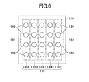
- FIG. 6 is a bottom view of the printed wiring board 100 from which the adhesive layer 170 and the radiator plate 180 are removed. Referring to FIG. 6 , the adhesive layer 170 and the radiator plate 180 are not attached to the back surface of the substrate 110 yet.
- FIG. 7 illustrates positions where the LEDs 190 are attached on FIG. 5 .
- 20 heat conductive portions 140 i.e., 5 in the lateral directions and 4 in the longitudinal directions, are arranged.
- the heat conductive portions 140 which are equal to 4 are connected to each of the wiring portions 130A to 130E which are equal to 5 in stripe-like shapes.
- the heat conductive portions 140 are positioned inside the area of the wiring portions 130A to 130E in the plan view and the bottom view of the printed wiring board 100. Referring to FIG. 5 , the heat conductive portions 140 which are equal to a plural number are arranged in the longitudinal directions of the wiring portions 130.
- the LEDs 190 which are equal to 16 are arranged so as to bridge neighboring two wiring potions 130 in the lateral directions. As described, by connecting the LEDs 190 to the wiring portions 130 via the plating layers 160A, four LEDs are connected in series in the lateral directions. It is possible to connect the four LEDs 190, which are connected in series, to the wirings 130 to form four rows in parallel arranged in the longitudinal directions.
- the protrusions 131 and 132 are formed in the two wiring portions 130A and 130E, respectively.
- the two wiring portions 130A and 130E are positioned on both ends of the arrangement of the five wiring portions 130A to 130E.
- the protrusions 131 and 132 are formed to protrude in the lateral directions so that the plating layers 160B1 and 160B2 are formed on the protrusions 131 and 132.
- the positive terminal of the power source is connected to one of the plating layers 160B1 and 160B2 (see FIG. 3 ) formed on the two protrusions 131 and 132 and the negative terminal of the power source is connected to the other one of the plating layers 160B1 and 160B2, the four rows of the four LEDs 190, which are connected in series, can be connected in parallel to the power source.
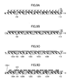
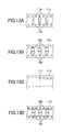
- FIGs. 8A to 13D are cross-sectional views of the printed wiring board 100 of the first embodiment for illustrating a process of manufacturing the printed wiring board of the first embodiment.
- the adhesive layer 120 is coated on the front surface (the upper surface in FIG. 8A ) of the substrate 110.
- an adhesive film may be attached to the front surface of the substrate 110.
- the substrate illustrated in FIG. 8A is wider than the substrate 110 in FIG. 2 on both side ends. Said differently, the substrate 110 protrudes right and left from the adhesive layer 120. The reason why the substrate 110 protrudes is to form sprocket holes on both side ends (to be described later).
- the longitudinal direction of the substrate 110 formed by a polyimide film is in a direction of penetrating the figure.
- the printed wiring board 100 can be manufactured by a reel-to-reel method using an insulative resin tape made of polyimide as a base material. Therefore, the substrate 110 in FIG. 8A illustrates a cross-sectional view of a part of a tape shaped substrate 113 illustrated in FIG. 10D illustrated later.
- five through holes 111 and two sprocket holes 112 are formed by a punching process.
- the five through holes 111 penetrate both of the substrate 110 and the adhesive layer 120.
- a copper foil 133 is attached onto the adhesive layer 120.
- the thickness of the copper foil 133 is, for example, 18 ⁇ m to 35 ⁇ m.
- the copper foil 133 is patterned to be wiring portions.
- portions of the lower surface of the copper foil 133 facing the through holes 111 and the upper surface of the copper foil 133 are etched.
- an anticorrosive agent on the surface of the copper foil 133 is removed, and the surface of the copper foil 133 is slightly removed in the thickness direction (for example, 1 to 2 ⁇ m). The etching process may be performed when it is preferable to do so.
- a masking tape 10 is attached to the upper surface of the copper foil 133.
- the heat conductive portions 140 are grown during electro plating.
- a plated metal deposits on the back surfaces of the copper foil 133 which are exposed inside the through holes 111.
- the heat conductive portions 140 made of the plated metal are formed in columnar shapes.
- the upper ends of the through holes 111 are blocked by the copper foil 133.
- the heat conductive portions in the columnar shapes are completed.
- the heat conductive portions 140 may be formed as follows. Copper plating deposits on the back surfaces of the copper foil 133 by electro copper plating, and the through holes 111 are filled with copper plating.
- the through holes 111 penetrate through both of the substrate 110 and the adhesive layer 120 thereby causing the back surfaces of the copper foil 133 to expose. Therefore, the heat conductive portions 140 penetrate through the substrate 110 and the adhesive layer 120, and are formed in a columnar shape.
- the front surfaces of the heat conductive portions 140 in FIG. 9A are connected to the copper foil 133.
- the back surfaces of the heat conductive portions 140 in FIG. 9A are exposed on the back surface of the substrate 110. Referring to FIG. 9A , the back surfaces of the heat conductive portions 140 protrude from the back surface of the substrate 110.
- the masking tape 10 covers the upper surfaces of the copper foil 133 to prevent a copper layer from growing on the upper surface of the copper foil 133 while the heat conductive portions 140 are grown with electro plating.
- the electro plating is performed by supplying electric power to the copper foils 133.
- the masking tape 10 is removed.
- a resist is coated on the copper foil 133 and exposed to light in conformity with the pattern of the wiring portions 130.
- the pattern of the wiring portions 130 is developed.
- the wiring portions 130 are formed (patterned) as illustrated in FIG. 9C .
- the developed resist is removed after patterning the wiring portions 130.
- an insulating layer 150 is formed on predetermined portions of the wiring portions 130 where plating layers 160A and 160B are not to be formed.
- the insulating layer 150 may be formed by a screen printing method. If the insulating layer 150 is other than the white-colored ink, the insulating layer 150 may be formed by a method other than the screen printing method or the like.
- the following method can be applied. After forming the insulating layer 150 to cover the wiring portions 130, there are formed opening portions in the insulating layer 150 through which the wiring portions 130 are exposed so that the plating layers 160A and 160B are formed on these.
- the end portion 130A1 of the wiring portion 130A is exposed on the wiring portions 130A. This is because the wiring portion 130A is supplied with electric power when the plating layers 160A and 160B are formed.
- a copper foil 20 and a masking tape 30, which is attached to the copper foil 20, are attached below the substrate 110. With this, the copper foil 20 contacts lower surfaces of the heat conductive portions 140. Thus, the lower surface of the substrate is completely covered by the masking tape 30.
- the leftmost wiring portion 130A is connected to the other four wiring portions 130B to 130E via the copper foil 20. Therefore, by supplying electric power to the end portion 130A1 of the wiring portion 130, the wiring portions 130B to 130E are also supplied with electric power.
- the plating layers 160A and 160B are formed.
- the plating layers 160A and 160B are formed by sequentially laminating a nickel (Ni) layer, and a gold (Au) layer in this order in the wiring portions 130.
- Ni nickel
- Au gold
- a nickel layer, a palladium layer, and a gold layer may be sequentially formed in this order.
- a nickel layer and a silver layer are sequentially formed in this order.
- another plating layer may be used.
- the end portion 130A1 of the wiring portion 130A is exposed on the insulating layer 150.
- Portions to which electric power is supplied are provided to form the plating layers 160A and 160B. These portions are not limited to the end portion 130A1 of the wiring portion and may be another portion for supplying electric power of the wiring portion 130A. Further, in addition to the wiring portions 130A to 130E, wirings, electrodes, or the like may be formed to supply electric power.
- a portion where the electric power is supplied is not limited to the end portion 130A1 of the wiring portion 130A for forming the plating layers 160A and 160B.
- the plating layers 160A and 160B may be formed by a method using a sparger.
- the masking tape 30 to which the copper foil 20 is attached is removed. With this, a portion of the printed wiring board 100 except for the adhesive layer 170 and the radiator plate 180 as illustrated in FIG. 2 is completed.
- the tape shaped substrate 113 formed by the polyimide tape is cut in its longitudinal direction.
- the wiring portion to be a printed wiring board 100 is indicated by a reference symbol 101.
- the wiring portion 101 includes plating layers 160A which are equal to 32 and the plating layers 160B1 and 160B2 illustrated in FIG. 1 .
- the tape shaped substrate 113 is cut so as to include the wiring portions 101 which are equal to 14.
- the tape shaped substrate 113A and 113B are divided across the width directions. Then, the divided tape shaped substrates 113A and 113B may be divided across the longitudinal directions as illustrated in FIG. 10D .
- a frame 181 on which plural radiator plates 180 are formed is prepared.
- the four corners of the radiator plate 180 are suspended by the frame 181 by wire-like connecting portions 182.
- the frame 181 may be formed by punching or etching a metallic material shaped like a hoop.
- FIG. 11A illustrates a part of the frame 181 in the longitudinal direction where radiator plates 180 which are equal to 6 are formed.
- the frame 181 extends right and left along the tape shaped substrate 113 (see FIG. 10D ).
- the adhesive layers 170 are coated on the radiator plates 180 formed in the frame 181.
- the tape shaped substrate 113 is attached onto on the frame 181. At this time, the adhesive layers 170 bond the radiator plates 180 to the tape shaped substrate 113.
- a glue film may be adhered to the radiator plates 180.
- the adhesive layer 120, the wiring portions 130, the heat conductive portions 140, the insulating layers 150, and the plating layers 160A and 160B are formed on the tape shaped substrate 113.
- a punching process or a dicing process is performed to make plural printed wiring boards 100 (see FIGs. 1 to 3 ).
- the frame 181 is separated by cutting connecting portions 182.
- a sheet-like product containing plural wiring portions 101 may be shipped.
- the adhesive layers 170 may be previously formed on the radiator plates 180. Then, the radiator plates 180 are bonded to the tape shaped substrates 113. However, the adhesive layer 170 may be previously formed on the tape shaped substrate 113.
- the adhesive layers 170 may be formed on the back surface of the tape shaped substrate 113.
- the frame 181 may be attached to the back surface of the tape shaped substrate.
- the adhesive layers 170 may be formed at positions corresponding to the wiring portions 101 (see FIG. 11C ).
- an adhesive layer 171 in a tape-like shape may be formed on the back surface of the tape shaped substrate 113.
- the frame 181 may be attached to the back surface of the tape shaped substrate 113.
- An adhesive agent may be coated instead of the adhesive layer 171.
- the radiator plate which has been previously diced may be attached to the back surface of the tape shaped substrate 113.
- the adhesive layer 170 may be attached to the back surface of the tape shaped substrate 113.
- the radiator plates 180 may be attached to the back surface of the tape shaped substrate 113.
- the adhesive layers 170 may be formed at positions corresponding to the wiring portions 101 (see FIG. 11C ).
- an adhesive layer 171 in a tape-like shape may be attached to the back surface of the tape shaped substrate 113.
- the radiator plates 180 may be attached to the back surfaces of the tape shaped substrate 113.
- An adhesive agent may be coated instead of the adhesive layer 171.
- a punching process or a dicing process is performed to dice to make plural printed wiring boards 100 (see FIGs. 1 to 3 ).
- a sheet-like product containing plural wiring portions 101 may be shipped.
- the printed wiring board 100 can be completely manufactured.
- the wiring portions 130 and the radiator plates 180 are thermally connected by the heat conductive portions 140. Since the heat conductive portions 140 are made of copper, heat conductivity is very high in comparison with the substrate made of polyimide. Further, the adhesive layers 170 for connecting the lower surfaces of the heat conductive portions 140 to the radiator plates 180 are an adhesive agent having high heat conductivity. Therefore, a thermal resistance between the heat conductive portions 140 and the radiator plates 180 can be reduced.
- heat generated by the electronic parts connected onto one surface of the substrate can be efficiently conducted to the radiator plate 180 provided on the other surface of the substrate 110.
- the heat generated by the electronic parts can be efficiently conducted to the radiator plate 180 provided on the other surface of the substrate 110.
- the printed wiring board 100 of which heat radiation property is greatly improved can be provided.
- the plating layers 160A are shaped like a semicircle in these plan views, and a circular electronic part element mounting portion is formed by a pair of plating layers 160A.
- the shapes of the plating layers 160A are not limited to shapes like the semicircle.
- the shapes of the plating layers 160A may be like a rectangle or the like.
- the shapes of the electronic part element mounting portions formed by the paired plating layers 160A in these plan views may be like a rectangle or the like.
- the wiring portions 130 may be formed as follows. At first, the metallic layer is directly formed on the substrate 110 made of an insulative resin film or the like as the base material such as polyimide by electroless plating, sputtering, electro plating or the like using copper or the like. Next, through holes are formed by the laser processing or the like on the insulative resin film, and the heat conductive portions 140 are formed by electro plating using the metallic layer as the power supply layer. Thereafter, the metallic layer may be etched to form the wiring portions 130.
- the wiring portions 130 may be formed by a method different from the above methods.
- An insulative resin film is formed by coating an insulative resin such as polyimide on a metallic foil such as a copper foil.
- the through holes are formed by laser processing or the like on the insulative resin film, and the heat conductive portions 140 are formed by electro plating using the metallic layer as the power supply layer.
- the metallic foil may be etched to form the wiring portions 130.
- a structure of mounting the LEDs 190 on the printed wiring board 100 and the printed wiring board 100 is mounted on the substrate of the lighting device.
- FIG. 14 is a cross-sectional view of a lighting device formed by mounting the LEDs 190 on the printed wiring board 100 of the first embodiment is mounted on the substrate of the lighting device.
- the light-emitting device 50 is formed by mounting the LEDs 190 on the printed wiring board 100 and includes the printed wiring board 100, the LEDs 190, and the encapsulating resin 191.
- the insulating plate 61 is arranged on the front surface of the basal plate 60 of the lighting device.
- the insulating plate 61 has an opening 61A.
- the insulating plate 61 also has a wiring 61B on its surface.
- the opening 61A is opened on the insulating plate 61 so as to have a rectangular shape in conformity with the size of the light-emitting device 50 in their plan views and penetrates through the insulating plate 61.
- a lead pin 63 is connected to the wiring 61B by a pin 61C.
- the basal plate 60 may be a member having a high heat radiation property such as an aluminum platelike member.
- the light-emitting device 50 is mounted on a basal plate 60 via silicone grease 62 and inside the opening portion 61A of the insulating plate 61.
- the lead pins 63 are provided right and left one each on the upper surface of the insulating plate 61.
- the lead pins 63 are connected to power input terminals of the lighting device.
- a pressing mechanism 64 is provided on the insulating plate 61 so as to press the lead pins in a downward direction of the lead pin 63.
- the pressing mechanism 64 includes a rotary shaft 64A and a turning portion 64B.
- the turning portion 64B is attached to the insulating plate 61 via the rotary shaft 64A so that the tuning portion 64B is rotatable between a position above the lead pin 63 (illustrated in FIG. 14 ) and a position apart from the lead pin 63 by the rotary shaft 64A.
- the turning portion 64B of the pressing mechanism 64 can be pushed in the downward direction in FIG. 14 while the tip of the lead pin contacts the plating layer 160B.
- the light-emitting device 50 can be fixed to the basal plate 60, and electric power can be supplied to the LEDs 190 via the lead pins 63 and the plating layers 160B.
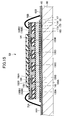
- FIG. 15 is a cross-sectional view of a modified example in which the light-emitting device, formed by mounting the LEDs 190 on the printed wiring board 100, is mounted on the basal plate 60 of the lighting device.
- the pressing mechanism 64 is used to mount the light-emitting device 50 on the basal plate 60 of the lighting device as one mode.
- the light-emitting device 50 may be connected to the basal plate 60 of the lighting device by the bonding wires 70A and 70B.
- the insulative layer 65, wirings 66A and 66B for power source and wiring 67 for radiation are formed on the upper surface of the basal plate 60.
- the insulative layer 65 is provided to insulate the wirings 66A, 66B, and 67 from the basal plate 60 made of aluminum or the like.
- the insulative layer 65 may be formed by a material which contains an epoxy adhesive and a ceramic filler.
- the wirings 66A, 66B, and 67 may be formed by patterning the copper foil attached to the upper surface of the insulative layer 65.
- the light-emitting device 50 is mounted on the basal plate 60 of the lighting device by connecting the radiator plate 180 to the wiring 67 via a bond 68.
- the bond 68 is preferably a bond having high heat conductivity such as silicone grease.
- the pair of plating layers 160B1 and 160B2 of the light-emitting device 50 are connected to the wirings 66A and 66B for power source by the bonding wires 70A and 70B, respectively.
- the light-emitting device 50 can be fixed to the basal plate 60, and electric power can be supplied to the LEDs 190 via the bonding wires 70A and 70B and the plating layers 160B1 and 160B2.
- the LEDs 190 are mounted in the printed wiring board 100 as the electronic part, the electronic parts are not limited to the LEDs 190.
- the electronic parts may be a light-emitting element such as a surface emitting laser.
- FIG. 16 is a cross-sectional view of a printed wiring board 100A of a modified example of the first embodiment.
- the printed wiring board 100A differs from the printed wiring board 100 of the first embodiment illustrated in FIG. 2 as follows.
- the radiator plate 180A is made of insulative material, and the surfaces of the heat conductive portions 140 are directly connected to the radiator plate 180A without the intervening adhesive layer 170 therebetween.
- the radiator plate 180A is a radiator plate made of a ceramic such as alumina or aluminum nitride or silicon. In a case where silicon is used, an insulative film such as an oxide film may be provided on the surface of the silicon.
- the radiator plate 180A made of the insulative material such as a ceramic may be connected to the wiring portions 130A to 130E via the heat conductive portions 140 without causing influences on electric potentials of the wiring portions 130A to 130E.
- the adhesive layer 170 does not intervene between the heat conductive portions 140 and the radiator plate 180A so that the heat conductive portions 140 are directly connected to the radiator plate 180A. Said differently, the other surface (the lower surface in FIG. 16 ) of the heat conductive portions 140 is pushed by the radiator plate 180A so as to directly contact the surface of the radiator plate 180A.
- the adhesive layer 170 may be previously patterned so as not to intervene between the heat conductive portions 140 and the radiator plate 180A.
- FIG. 17 is a cross-sectional view of a printed wiring board 100B of another modified example of the first embodiment. In a manner similar to FIG. 5 , FIG. 17 illustrates the printed wiring board 100B from which the insulating layer 150 and the plating layers 160A and 160B are removed.
- heat conductive portions 141 are shaped like a rectangle in this plan view.
- the printed wiring board 100B differs from the printed wiring board 100 of the first embodiment illustrated in FIG. 5 as follows.
- the heat conductive portions 141 are connected to the wiring portions 130A to 130E, respectively.
- the shapes of the heat conductive portions 141 are circular.
- the heat conductive portions which are equal to 4 are connected to each of the wiring portions 130A to 130E.
- the heat conductive portions 141 which are equal to 5 are formed in the longitudinal directions of the wiring portions 130A to 130E on substantially entire areas where the plating layers 160A are formed (see FIG. 17 ), respectively. Said differently, the heat conductive portions 141 are formed on the areas where the heat conductive portions 140 are formed with respect to the wiring portions of the first embodiment with respect to the wiring portions 130A to 130E illustrated in FIG. 5 , respectively.
- the printed wiring board 100B including the heat conductive portions 141 in a long and thin rectangular shape heat generated by electronic parts connected to the plating layers 160A can be efficiently conducted to the radiator plate 180 via the plating layers 160A, the heat conductive portion 141, and the adhesive layer 170. Therefore, heat radiation property can be greatly improved.
- FIG. 18 is a plan view of a printed wiring board of the second embodiment.
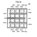
- FIG. 19 is a cross-sectional view of the wiring pattern of a printed wiring board of the second embodiment.
- FIG. 19 illustrates the pattern of wiring portions 230A to 230Q where the insulating layer 150 and the plating layers 260A, 260B1 and 260B2 are removed from FIG. 18 .
- the structure of the printed wiring board 200 of the second embodiment other than the above is similar to the printed wiring board 100 of the first embodiment. Therefore, the same reference symbols are attached to the same or similar constructional elements and description of these constructional elements is omitted.
- positions where the plating layers 260A, 260B1, and 260B2 arranged are illustrated by broken lines, and positions where the LEDs 190 connected are illustrated by heavy broken line.
- the plating layers 260A which are equal to 32 and the plating layers 260B1 and 260B2 are exposed on the insulting layer 150.
- the plating layers 260A which are equal to 32 are arranged in a manner similar to the plating layers 160A which are equal to 32 illustrated in FIG. 1 .
- the plating layers 260B1 and 260B2 are arranged on the right side end of FIG. 18 .
- the wiring portions 230A, 230B, 230C, 230D, 230E, 230F, 230G, 230H, 230I, 230J, 230K, 230L, 230M, 230N, 2300, 230P, and 230Q are formed on the adhesive layer 120.
- the wiring portions 230A to 230Q are arranged as follows.
- the wiring portions 230A to 230D are linearly arranged from right to left.
- the wiring portions 230E are linearly arranged from left to right.
- the wiring portions 230I to 230H are linearly arranged from left to right.
- the wiring portions 230J to 230P are arranged in a pattern similar to the wiring portions 230B to 230H. The arrangement ends at the wiring portion 230Q.
- the plating layers 260A which are equal to 32 are formed in a manner similar to the plating layers 160A in a semicircular shape as in the first embodiment so as to form circles which are equal to 16 (see FIG. 18 ).
- a pair of the plating layers 260A forming the circles which are equal to 16 are connected to different wiring portions 230A to 230Q.
- the plating layers 260B1 and 260B2 are formed on the wiring portions 230A and 230Q, respectively.
- the heat conductive portions 140 are arranged below the wiring portions 230A to 230Q.
- a positive terminal and a negative terminal of each electronic part are connected to each pair of the plating layers 260A, respectively.
- the negative terminals and the positive terminals of the electronic parts are alternatively connected to the plating layers 260A which are equal to 32 formed on the wiring portions 230A to 230Q.
- the negative terminals and the positive terminals of the power source are connected to the plating layers 260B1 and 260B2, respectively.
- the electronic parts which are equal to 16 are connected to the power source between the plating layers 260B1 and 260B2 in series.
- the heat generated by the electronic parts connected on one surface of the substrate 110 can be efficiently conducted to the radiator plate 180 provided on the other surface of the substrate 110.
- the printed wiring board 200 of which heat radiation property is greatly improved can be provided.
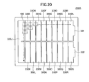
- FIG. 20 is a cross-sectional view of the wiring pattern of a printed wiring board of a modified example of the second embodiment.
- the wiring pattern of the printed wiring board 200A of the modified example of the second embodiment differs from the printed wiring board 200 illustrated in FIG. 19 .
- the other structure of the modified example is similar to the printed wiring board 200 of the second embodiment.
- the wiring portions 330A and 330S have protrusions 331 and 332, respectively.
- the protrusion 331 and 332 in a manner similar to the protrusions 131 and 132 (see FIG. 3 ), plating layers connected to the power source (plating layers similar to the plating layers 160B1 and 160B2 of the first embodiment) are formed.
- the wiring portions 330A to 330S which are equal to 19 are shaped like stripes.
- the wiring portion 330J has a length in the longitudinal direction substantially twice as long as the lengths of the other wiring portions in the longitudinal directions.
- the wiring portions 330A to 330I are arranged right to left.
- the wirings 330K to 330S are arranged from left to right on a side lower than the wiring portions 330A to 330I.
- the wiring portion 330J is arranged on the left side of the wiring portions 330I and 330K.
- the wiring portions 330A to 330S have plating layers similar to the plating layer 260A in conformity with the positions where the electronic parts are mounted.
- the heat conductive portions 140 are arranged below the wiring portions 330A to 330S.
- the positive terminals and the negative terminals of the electronic parts are connected to the plating layers (similar to the plating layers 260A) formed on the adjacent wiring portions 330A to 330S arranged in the lateral direction.
- the plating layers similar to the plating layers 160B1 and 160B2 of the first embodiment
- electric power may be supplied to many electronic parts from the power source.
- heat generated by the electronic parts can be efficiently conducted to the radiator plate 180 from the plating layers (similar to the plating layers 260A) via the heat conductive portions 140.
- heat radiation property can be greatly improved.
- the heat generated by the electronic parts connected on one surface of the substrate 110 can be efficiently conducted to the radiator plate 180 provided on the other surface of the substrate 110.
- the printed wiring board 200A of which the heat radiation property is greatly improved can be provided.
- a printed wiring board which can efficiently transfer heat generated by electronic parts, which are connected to one surface of the substrate, to a radiator plate disposed on another surface of the substrate.
Landscapes
- Engineering & Computer Science (AREA)
- Microelectronics & Electronic Packaging (AREA)
- Manufacturing & Machinery (AREA)
- Led Device Packages (AREA)
- Structure Of Printed Boards (AREA)
- Printing Elements For Providing Electric Connections Between Printed Circuits (AREA)
Abstract
Description
- The embodiments discussed herein are related to a printed wiring board and a method of manufacturing the printed wiring board.
- There is an exemplary lighting device formed by mounting plural LED groups including plural light emitting diodes (LEDs) on a wiring pattern provided on a front surface of a substrate having flexibility and mounting plural radiator plates on a back surface opposite to the front surface on which the plural LED groups are mounted as disclosed in, for example, Japanese Laid-open Patent Publication No.
2003-092011 - The plural radiator plates are bonded to the substrate by an adhesive so as to cover portions corresponding to mounting positions of the plural LED groups.
- As described, the exemplary lighting device is formed by mounting the LEDs on the printed wiring board including the substrate, a wiring pattern (wiring portions), and a radiator plate.
- However, in the printed wiring board of the exemplary lighting device, the wiring portions are connected to the radiator plate via the substrate. The substrate is made of a resin having a low heat conductivity (for example, fiber-glass reinforced plastic).
- Therefore, there is a problem that heat generated by electronic parts generating heat such as LEDs is not efficiently conducted to the radiator plates on the back surface of the substrate from the wiring portions on the front surface of the substrate.
- The object of the present invention is to provide a printed wiring board which can efficiently transfer heat generated by electronic parts, which are connected to one surface of the substrate, to a radiator plate disposed on another surface of the substrate.
- According to an aspect of the embodiment, a printed wiring board includes an insulative substrate, a wiring portion which is formed on a surface of the insulative substrate and has a predetermined wiring pattern, an insulative layer which is formed on the wiring portion and on which a part of the wiring layer is exposed as a terminal, a radiator plate provided on another surface of the insulative substrate, and a heat conductive portion which is formed inside the through hole penetrating through the surface and the other surface of the insulative substrate and connected to the wiring portion
-
FIG. 1 is a plan view of a printed wiring board of a first embodiment; -
FIG. 2 is a cross-sectional view of the printed wiring board of the first embodiment; -
FIG. 3 is a plan view from which an insulating layer is removed from a printed wiring board; -
FIG. 4 is a cross-sectional view of the printed wiring board of the first embodiment on which LEDs are mounted; -
FIG. 5 illustrates the position, the size and the shape of a heat conductive portion on the printedwiring board 100 of the first embodiment; -
FIG. 6 illustrates the position, the size and the shape of the heat conductive portion on the printed wiring board of the first embodiment; -
FIG. 7 illustrates the position, the size and the shape of the heat conductive portion on the printed wiring board of the first embodiment; -
FIGs. 8A-8D are cross-sectional views of the printed wiring board of the first embodiment for illustrating a process of manufacturing the printed wiring board of the first embodiment; -
FIGs. 9A-9D are cross-sectional views of the printed wiring board of the first embodiment for illustrating the process of manufacturing the printed wiring board of the first embodiment; -
FIGs. 10A-10E are cross-sectional views of the printed wiring board of the first embodiment for illustrating the process of manufacturing the printed wiring board of the first embodiment; -
FIGs. 11A-11C are cross-sectional views of the printed wiring board of the first embodiment for illustrating the process of manufacturing the printed wiring board of the first embodiment; -
FIGs. 12A-12C are cross-sectional views of the printed wiring board of the first embodiment for illustrating the process of manufacturing the printed wiring board of the first embodiment; -
FIGs. 13A-13D are cross-sectional views of the printed wiring board of the first embodiment for illustrating the process of manufacturing the printed wiring board of the first embodiment; -
FIG. 14 is a cross-sectional view of a lighting device where a light-emitting device formed by mounting the LEDs on the printed wiring board of the first embodiment is mounted on the substrate of the lighting device; -
FIG. 15 is a cross-sectional view of a modified example of the lighting device where the light-emitting device formed by mounting the LEDs on the printed wiring board of the first embodiment is mounted on the substrate of the lighting device; -
FIG. 16 is a cross-sectional view of a printed wiring board of a modified example of the first embodiment; -
FIG. 17 is a cross-sectional view of a printed wiring board of another modified example of the first embodiment; -
FIG. 18 is a plan view of a printed wiring board of a second embodiment; -
FIG. 19 is a cross-sectional view of the wiring pattern of a printed wiring board of the second embodiment; and -
FIG. 20 is a cross-sectional view of the wiring pattern of a printed wiring board of a modified example of the second embodiment. - Preferred embodiments of the present invention will be explained with reference to accompanying drawings.
-
FIG. 1 is a plan view of a printed wiring board of the first embodiment.FIG. 2 is a cross-sectional view of the printed wiring board of the first embodiment. The cross-sectional view illustrated inFIG. 2 is taken along a line 2-2 ofFIG. 1 . - The printed
wiring board 100 of the first embodiment includes asubstrate 110,adhesive layer 120,wiring portions 130, heatconductive portions 140, aninsulating layer 150,plating layers adhesive layer 170, and aradiator plate 180. - Referring to
FIG. 1 , theplating layers 160A, 160B1, and 160B2 are exposed on theinsulating layer 150.FIG. 3 is a plan view from which theinsulating layer 150 is removed from the printedwiring board 100 illustrated inFIG. 1 . Referring toFIG. 3 , this state does not exist in a process of manufacturing the printedwiring board 100 to be described later. However,FIG. 3 is illustrated in order to facilitate understanding of the printedwiring board 100 illustrated inFIG. 1 without theinsulating layer 150. Thus, positional relationships among theadhesive layer 120, thewiring portions 130, and theplating layers 160A, 160B1, and 160B2 are illustrated without theinsulating layer 150. - For example, the
substrate 110 is preferably made of a polyimide tape, which is an insulative resin film. The polyimide tape is an example of insulative substrates. The polyimide tape has flexibility. Further, because the polyimide tape is a tape-like film made of polyimide, the polyimide tape can be preferably used to dice the tape-like film to make plural printedwiring boards 100 after forming the plural printedwiring boards 100. - However, the
substrate 110 may be made of not only the polyimide tape but also an insulative resin film made of a different type of the insulative resin film. For example, a film made of an epoxy resin or a polyester resin may be used. - However, the
substrate 110 is not limited to the polyimide tape or the insulative substrate having flexibility. For example, thesubstrate 110 may be made of a glass epoxy resin according to the standard of Flame Retardant 4 (FR4). - The thickness of the substrate is, for example, 50 µm to 125 µm.
- The
adhesive layer 120 is attached to the front surface (i.e., an upper surface inFIG. 2 ) of thesubstrate 110. Thewiring portions 130 are bonded to thesubstrate 110 by theadhesive layer 120. Theadhesive layer 120 may be made of, for example, a heat resistant resin such as an epoxy adhesive or a polyimide adhesive. The thickness of theadhesive layer 120 is, for example, 8 µm to 12 µm. - The
wiring portions 130 are bonded to the surface of thesubstrate 110 by theadhesive layer 120 and are patterned to be a predetermined pattern.FIG. 3 illustrates fivewiring portions 130A to 130E patterned to be in a stripe-like shape. Among thewiring portions 130A to 130E, thewiring portions protrusions - The
wiring portions 130 are shaped like a ruler or a rectangle in their plan views. Theplural wiring portions 130 are formed so that long sides of theplural wiring portions 130 face one another with interposing predetermined gaps. Theplural wiring portions 130 are arranged in parallel so that long sides of long and thin portions face one another. - The
wiring portions 130A to 130E are formed under the plating layers 160A, 160B1, and 160B2 as illustrated inFIG. 2 . - For example, the
wiring portions 130A to 130E may be formed by patterning a copper foil attached to the surface of thesubstrate 110 by theadhesive layer 120. - The lengths of the
wiring portions 130A to 130E are, for example, 5.0 mm to 10.00 mm. The widths of thewiring portions 130A to 130E are, for example, 0.5 mm to 1.0 mm. The thicknesses of thewiring portions 130A to 130E are, for example, 18 µm to 35 µm. - Hereinafter, if the
wiring portions 130A to 130E are not independently distinguished, thewiring portions 130A to 130E are integrally referred to as thewiring portion 130. - The heat
conductive portions 140 are shaped like columns (posts) formed inside through holes of thesubstrate 110 from the back surface to the front surface. The through holes also penetrate theadhesive layer 120. The upper ends of the heatconductive portions 140 are connected to thewiring portions 130. The lower ends of the heatconductive portions 140 are connected to theradiator plate 180 via theadhesive layer 170. The shapes of the heatconductive portions 140 in its plan views are circular. Said differently, the heatconductive portions 140 are conductive and shaped like cylindrical columns. - The heat
conductive portions 140 are, for example, copper column-shaped members. The heatconductive portions 140 are formed by growing plating metal inside the through holes of thesubstrate 110 by electro plating. The diameter of the heatconductive portions 140 are, for example, 0.2 mm to 0.8 mm. The shapes of the heatconductive portions 140 in their plan views are not limited to circles and may be ellipses, rectangles, polygons or the like. Therefore, the heat conductive portions are not limited to be shaped like cylindrical columns, and may be shaped like rectangular columns. - The front surfaces of the heat
conductive portions 140 inFIG. 4 are connected to thewiring portions 130. The back surfaces of the heatconductive portions 140 inFIG. 4 are exposed on the back surface of thesubstrate 110. For example, the back surfaces of the heatconductive portions 140 protrude from the back surfaces of thesubstrate 110 and face theradiator plate 180 via theadhesive layer 170. - The back surfaces of the heat conductive portions and the back surface of the
substrate 110 may be leveled. Instead, the back surfaces of the heat conductive portions may be set back from the back surface of thesubstrate 110 toward the insides of the through holes. - The positions of the heat
conductive portions 140, the detailed shapes of theconductive portions 140 or the like may be described later with reference toFIGs. 5-7 . - The insulating
layer 150 is formed so as to cover portions of the front surface of theadhesive layer 120 which are not covered by thewiring portions 130 inFIG. 2 and portions of the front surfaces of thewiring portions 130 which are not covered by the plating layers 160A, 160B1, and 160B2 inFIG. 2 . - For example, the insulating
layer 150 is a white-colored insulative resin in a case where an electronic part having luminescent and thermogenetic properties such as a LED is mounted on or above the insulatinglayer 150 using theplating layer 160A of the printed wiring board of the first embodiment. By making the color of the insulatinglayer 150 white, it is possible to improve the reflectance and the heat radiation rate of the insulatinglayer 150. Further, it is also possible to improve the illumination intensity and the heat radiation property. Said differently, the insulatinglayer 150 functions as a reflective film. - The insulative resin forming the insulating
layer 150 may be obtained by adding a filler or a pigment such as titanium oxide (TiO2) or barium sulfate (BaSO4) to, for example, an epoxy resin or a silicone resin such as organopolysiloxane. The insulative resin of the insulatinglayer 150 may be a white ink made of the material of the insulative resin. - The insulating
layer 150 may be configured to electrically insulate portions of the front surfaces of thewiring portions 130 on which the plating layers 160A, 160B1, and 160B2 are not formed inFIG. 2 . Various insulating layers other than a white-colored ink layer depending on the types of the electronic part connected to the plating layers 160A. - The insulating
layer 150 is formed so as to expose areas of thewiring portions 130, on which the plating layers 160A, 160B1, and 160B2 are formed, before the plating layers 160A, 160B1, and 160B2 are formed. - The plating layers 160A are formed on the portions of the front surfaces of the wiring portions, which are not covered by the insulating
layer 150. The plating layers 160A are used as electrodes for connecting terminals of the electronic parts. - Referring to
FIGs. 1 and3 , platinglayers 160A which are equal to 32 are illustrated. The plating layers 160A are formed inside semicircle areas in these plan views. The plating layers 160A which are equal to 32 are arranged to form circles which are equal to 16. A pair of platinglayers 160A forming the circles which are equal to 16 are formed ondifferent wiring portions 130A to 130E (seeFIG. 3 ). Therefore, the plating layers 160A which are equal to 8 (partly illustrated in their cross-sectional views) constitute four pairs in each of thewiring portions 130A to 130E. - For example, the positive terminal and the negative terminal are respectively connected to the pair of plating
layers 160A. For example, referring toFIGs. 1 and3 , the negative terminal of the electronic part is connected to the left terminal of the pair of platinglayers 160A, and the positive terminal of the electronic part is connected to the right terminal of the pair of platinglayers 160A. - By connecting as such, the electronic parts which are equal to 4, which are connected to the plating layers 160A which are equal to 8 arranged in the lateral direction in
FIGs. 1 and3 , are connected in series. Further, the electronic parts which are equal to 4 can be connected in parallel. - Referring to
FIGs. 1 and3 , the plating layers 160B1 and 160B2 are provided inprotrusions wiring portions layers 160A which are equal to 16 pairs. - Hereinafter, if the plating layers 160B1 and 160B2 are not independently distinguished, the plating layers 160B1 and 160B2 are integrally referred to as the plating layers 160B.
- The
adhesive layer 170 is attached to the back surface (i.e., a lower surface inFIG. 2 ) of thesubstrate 110. Theradiator plate 180 is bonded to thesubstrate 110 by theadhesive layer 170. It is preferable that theadhesive layer 170 has high heat conductivity. Theadhesive layer 170 may be a heat radiation bond in which a filler such as alumina is contained in an insulative resin such as an epoxy resin or a polyimide resin. - The
radiator plate 180 is a heat spreader attached to the back surface of thesubstrate 110 by theadhesive layer 170. Theradiator plate 180 is, for example, a metallic plate made of a metallic material such as aluminum, copper, or the like; ceramics such as alumina, aluminum nitride or the like; or an insulating plate made of an insulating material having high heat conductivity such as silicon or the like. -
FIG. 4 illustrates a light-emitting device formed by mountingLEDs 190 on the printedwiring board 100 of the first embodiment.FIG. 4 is a cross-sectional view of the printedwiring board 100 of the first embodiment on whichLEDs 190 are mounted. The cross-sectional view illustrated inFIG. 4 corresponds to the cross-sectional view illustrated inFIG. 2 . - Referring to
FIG. 4 , eachLED 190 is connected to the corresponding one of the four pairs of the plating layers 160A which are equal to 8. TheLEDs 190 include electrodes (not illustrated). Theterminals LEDs 190 are connected to thewiring portions 130 via the plating layers 160A and theterminals - The
terminals LEDs 190 which are equal to 4 are respectively connected to the four pairs of the plating layers 160A which are equal to 8. The plating layers 160A may be connected to theterminals - The
LEDs 190 are sealed by a encapsulatingresin 191. The encapsulatingresin 191 may be formed by, for example, fluorescent material. The material of the fluorescent material may be determined based on a relationship between the fluorescent material and the luminescent color of theLED 190. For example, if a white luminescent color is to be obtained by the light-emitting device formed by mounting theLEDs 190 and the encapsulatingresin 191 on the printedwiring board 100, for example, theLEDs 190 emitting blue light are used and the material of the encapsulatingresin 191 is fluorescent material having luminescent colors of green and red. - For example, the encapsulating
resin 191 may be formed by adding fluorescent material to a silicone resin or an epoxy resin. TheLEDs 190 are sealed by molding or potting using the above-mentioned resin. - Referring to
FIG. 4 , the heatconductive portions 140 are provided immediately below the portions of thewiring portions 130 to which the terminals of theLEDs 190 are connected (portions of the plating layers 160). Therefore, a path for radiating heat is shortened to thereby improve a heat radiation property. - However, the positions of the heat
conductive portions 140 are not limited to the positions immediately below the portions of the wiring portions 130 (the portions of the plating layers 160) to which theterminals LEDs 190 are connected. - Referring to
FIG. 4 , the fourLEDs 190 are integrally sealed by the encapsulatingresin 191. The encapsulatingresin 191 may be provided for eachLED 190 or a group of some of theLEDs 190. -
FIG. 5 to FIG. 7 illustrate the positions, the sizes and the shapes of the heatconductive portions 140 on the printedwiring board 100 of the first embodiment. - Referring to
FIG. 5 , the insulatinglayer 150 and the plating layers 160A and 160B are removed fromFIG. 1 .FIG. 6 is a bottom view of the printedwiring board 100 from which theadhesive layer 170 and theradiator plate 180 are removed. Referring toFIG. 6 , theadhesive layer 170 and theradiator plate 180 are not attached to the back surface of thesubstrate 110 yet.FIG. 7 illustrates positions where theLEDs 190 are attached onFIG. 5 . - Referring to
FIGs. 5 and6 ,20 heatconductive portions 140, i.e., 5 in the lateral directions and 4 in the longitudinal directions, are arranged. The heatconductive portions 140 which are equal to 4 are connected to each of thewiring portions 130A to 130E which are equal to 5 in stripe-like shapes. The heatconductive portions 140 are positioned inside the area of thewiring portions 130A to 130E in the plan view and the bottom view of the printedwiring board 100. Referring toFIG. 5 , the heatconductive portions 140 which are equal to a plural number are arranged in the longitudinal directions of thewiring portions 130. - As indicated by thick broken lines, the
LEDs 190 which are equal to 16 are arranged so as to bridge neighboring two wiringpotions 130 in the lateral directions. As described, by connecting theLEDs 190 to thewiring portions 130 via the plating layers 160A, four LEDs are connected in series in the lateral directions. It is possible to connect the fourLEDs 190, which are connected in series, to thewirings 130 to form four rows in parallel arranged in the longitudinal directions. - The
protrusions wiring portions wiring portions wiring portions 130A to 130E. Theprotrusions protrusions - Therefore, when the positive terminal of the power source is connected to one of the plating layers 160B1 and 160B2 (see
FIG. 3 ) formed on the twoprotrusions LEDs 190, which are connected in series, can be connected in parallel to the power source. - Referring to
FIGs. 8A to 12C , the manufacturing method of the printedwiring board 100 of the first embodiment is described. -
FIGs. 8A to 13D are cross-sectional views of the printedwiring board 100 of the first embodiment for illustrating a process of manufacturing the printed wiring board of the first embodiment. - Referring to
FIG. 8A , theadhesive layer 120 is coated on the front surface (the upper surface inFIG. 8A ) of thesubstrate 110. Instead of coating theadhesive layer 120, an adhesive film may be attached to the front surface of thesubstrate 110. - The substrate illustrated in
FIG. 8A is wider than thesubstrate 110 inFIG. 2 on both side ends. Said differently, thesubstrate 110 protrudes right and left from theadhesive layer 120. The reason why thesubstrate 110 protrudes is to form sprocket holes on both side ends (to be described later). The longitudinal direction of thesubstrate 110 formed by a polyimide film is in a direction of penetrating the figure. - For example, the printed
wiring board 100 can be manufactured by a reel-to-reel method using an insulative resin tape made of polyimide as a base material. Therefore, thesubstrate 110 inFIG. 8A illustrates a cross-sectional view of a part of a tape shapedsubstrate 113 illustrated inFIG. 10D illustrated later. - Referring to
FIG. 8B , five throughholes 111 and twosprocket holes 112 are formed by a punching process. The five throughholes 111 penetrate both of thesubstrate 110 and theadhesive layer 120. - Next, as illustrated in
FIG. 8C , acopper foil 133 is attached onto theadhesive layer 120. The thickness of thecopper foil 133 is, for example, 18 µm to 35 µm. Thecopper foil 133 is patterned to be wiring portions. - Referring to
FIG. 8D , by impregnating the printedwiring board 100 with a solution for wet etching, portions of the lower surface of thecopper foil 133 facing the throughholes 111 and the upper surface of thecopper foil 133 are etched. By etching the printedwiring board 100, an anticorrosive agent on the surface of thecopper foil 133 is removed, and the surface of thecopper foil 133 is slightly removed in the thickness direction (for example, 1 to 2 µm). The etching process may be performed when it is preferable to do so. - Referring to
FIG. 9A , a maskingtape 10 is attached to the upper surface of thecopper foil 133. The heatconductive portions 140 are grown during electro plating. A plated metal deposits on the back surfaces of thecopper foil 133 which are exposed inside the throughholes 111. Thus, the heatconductive portions 140 made of the plated metal are formed in columnar shapes. Before the heatconductive portions 140 are formed, the upper ends of the throughholes 111 are blocked by thecopper foil 133. - By filling the through
holes 111 with the plated metal, the heat conductive portions in the columnar shapes are completed. For example, the heatconductive portions 140 may be formed as follows. Copper plating deposits on the back surfaces of thecopper foil 133 by electro copper plating, and the throughholes 111 are filled with copper plating. - The through
holes 111 penetrate through both of thesubstrate 110 and theadhesive layer 120 thereby causing the back surfaces of thecopper foil 133 to expose. Therefore, the heatconductive portions 140 penetrate through thesubstrate 110 and theadhesive layer 120, and are formed in a columnar shape. - The front surfaces of the heat
conductive portions 140 inFIG. 9A are connected to thecopper foil 133. The back surfaces of the heatconductive portions 140 inFIG. 9A are exposed on the back surface of thesubstrate 110. Referring toFIG. 9A , the back surfaces of the heatconductive portions 140 protrude from the back surface of thesubstrate 110. - The masking
tape 10 covers the upper surfaces of thecopper foil 133 to prevent a copper layer from growing on the upper surface of thecopper foil 133 while the heatconductive portions 140 are grown with electro plating. The electro plating is performed by supplying electric power to the copper foils 133. - Next, referring to
FIG. 9B , the maskingtape 10 is removed. - Next, a resist is coated on the
copper foil 133 and exposed to light in conformity with the pattern of thewiring portions 130. Thus, the pattern of thewiring portions 130 is developed. By etching using the developed resist, thewiring portions 130 are formed (patterned) as illustrated inFIG. 9C . Referring toFIG. 9C , the developed resist is removed after patterning thewiring portions 130. - Referring to
FIG. 9D , an insulatinglayer 150 is formed on predetermined portions of thewiring portions 130 where plating layers 160A and 160B are not to be formed. For example, if the insulatinglayer 150 is a white-colored ink, the insulatinglayer 150 may be formed by a screen printing method. If the insulatinglayer 150 is other than the white-colored ink, the insulatinglayer 150 may be formed by a method other than the screen printing method or the like. - As to the insulating
layer 150, besides the screen printing method, the following method can be applied. After forming the insulatinglayer 150 to cover thewiring portions 130, there are formed opening portions in the insulatinglayer 150 through which thewiring portions 130 are exposed so that the plating layers 160A and 160B are formed on these. - Referring to
FIG. 9D , by removing edges of the insulating layer 150 (the left edge ofFIG. 9D ), the end portion 130A1 of thewiring portion 130A is exposed on thewiring portions 130A. This is because thewiring portion 130A is supplied with electric power when the plating layers 160A and 160B are formed. - Referring to
FIG. 10A , acopper foil 20 and amasking tape 30, which is attached to thecopper foil 20, are attached below thesubstrate 110. With this, thecopper foil 20 contacts lower surfaces of the heatconductive portions 140. Thus, the lower surface of the substrate is completely covered by the maskingtape 30. - For example, electric power is supplied to the end portion 130A1 which is not covered by the insulating
layer 150 of theleftmost wiring portion 130 among the fivewiring portions 130A to 130E. Under this state, theleftmost wiring portion 130A is connected to the other fourwiring portions 130B to 130E via thecopper foil 20. Therefore, by supplying electric power to the end portion 130A1 of thewiring portion 130, thewiring portions 130B to 130E are also supplied with electric power. - Therefore, under the state illustrated in
FIG. 10A , electro plating is performed while supplying electric power to all of thewiring portions 130A to 130E via the end portion 130A1 of thewiring portion 130A. Thus, as illustrated inFIG. 10B , the plating layers 160A and 160B are formed. The plating layers 160A and 160B are formed by sequentially laminating a nickel (Ni) layer, and a gold (Au) layer in this order in thewiring portions 130. For example, a nickel layer, a palladium layer, and a gold layer may be sequentially formed in this order. A nickel layer and a silver layer are sequentially formed in this order. As described, another plating layer may be used. - Referring to
FIG. 9D to FIG. 10B , by removing left side ends of the insulatinglayer 150, the end portion 130A1 of thewiring portion 130A is exposed on the insulatinglayer 150. Portions to which electric power is supplied are provided to form the plating layers 160A and 160B. These portions are not limited to the end portion 130A1 of the wiring portion and may be another portion for supplying electric power of thewiring portion 130A. Further, in addition to thewiring portions 130A to 130E, wirings, electrodes, or the like may be formed to supply electric power. - Said differently, as long as the electric power can be supplied to all
wiring portions 130A to 130E via themasking tape 30, to which the copper foil is attached as illustrated inFIG. 10A by supplying electric power to any one of thewiring portions 130A to 130E, a portion where the electric power is supplied is not limited to the end portion 130A1 of thewiring portion 130A for forming the plating layers 160A and 160B. - As described, there is explained the process of forming the plating layers 160A and 160B in the electroplating while supplying power to the
wiring portions 130A to 130E via the end portion 130A1 of thewiring portion 130A. However, if the end portion 130A1 of the wiring portion 130A1 is not exposed on the insulatinglayer 150, for example, the plating layers 160A and 160B may be formed by a method using a sparger. - Next, referring to
FIG. 10C , the maskingtape 30 to which thecopper foil 20 is attached is removed. With this, a portion of the printedwiring board 100 except for theadhesive layer 170 and theradiator plate 180 as illustrated inFIG. 2 is completed. - Next, referring to
FIG. 10D , the tape shapedsubstrate 113 formed by the polyimide tape is cut in its longitudinal direction. Referring toFIG. 10D , the wiring portion to be a printedwiring board 100 is indicated by areference symbol 101. Thewiring portion 101 includes platinglayers 160A which are equal to 32 and the plating layers 160B1 and 160B2 illustrated inFIG. 1 . In the process illustrated inFIG. 10D , the tape shapedsubstrate 113 is cut so as to include thewiring portions 101 which are equal to 14. - Referring to
FIG. 10E , when thewiring portions 101 which are equal to 4 are formed in the width directions of the tape shapedsubstrate 113, the tape shapedsubstrate substrates FIG. 10D . - Referring to
FIG. 11A , aframe 181 on whichplural radiator plates 180 are formed is prepared. The four corners of theradiator plate 180 are suspended by theframe 181 by wire-like connectingportions 182. Theframe 181 may be formed by punching or etching a metallic material shaped like a hoop. -
FIG. 11A illustrates a part of theframe 181 in the longitudinal direction whereradiator plates 180 which are equal to 6 are formed. Theframe 181 extends right and left along the tape shaped substrate 113 (seeFIG. 10D ). - Referring to
FIG. 11B , theadhesive layers 170 are coated on theradiator plates 180 formed in theframe 181. Referring toFIG. 11C , the tape shapedsubstrate 113 is attached onto on theframe 181. At this time, theadhesive layers 170 bond theradiator plates 180 to the tape shapedsubstrate 113. Instead of theadhesive layers 170, a glue film may be adhered to theradiator plates 180. - The
adhesive layer 120, thewiring portions 130, the heatconductive portions 140, the insulatinglayers 150, and the plating layers 160A and 160B (seeFIG. 2 ) are formed on the tape shapedsubstrate 113. - After the process illustrated in
FIG. 11C , a punching process or a dicing process is performed to make plural printed wiring boards 100 (seeFIGs. 1 to 3 ). At this time, theframe 181 is separated by cutting connectingportions 182. - Instead of dicing to form the printed
wiring board 100, a sheet-like product containingplural wiring portions 101 may be shipped. - Referring to
FIG. 11A to 11C , theadhesive layers 170 may be previously formed on theradiator plates 180. Then, theradiator plates 180 are bonded to the tape shapedsubstrates 113. However, theadhesive layer 170 may be previously formed on the tape shapedsubstrate 113. - Referring to
FIG. 12A , theadhesive layers 170 may be formed on the back surface of the tape shapedsubstrate 113. Next, as illustrated inFIG. 12C , theframe 181 may be attached to the back surface of the tape shaped substrate. Theadhesive layers 170 may be formed at positions corresponding to the wiring portions 101 (seeFIG. 11C ). - Referring to
FIG. 12B , anadhesive layer 171 in a tape-like shape may be formed on the back surface of the tape shapedsubstrate 113. Next, as illustrated inFIG. 12C , theframe 181 may be attached to the back surface of the tape shapedsubstrate 113. An adhesive agent may be coated instead of theadhesive layer 171. - Referring to
FIGs. 13A-13D , the radiator plate which has been previously diced may be attached to the back surface of the tape shapedsubstrate 113. - Referring to
FIG. 13A , theadhesive layer 170 may be attached to the back surface of the tape shapedsubstrate 113. Next, as illustrated inFIG. 13B , theradiator plates 180 may be attached to the back surface of the tape shapedsubstrate 113. Theadhesive layers 170 may be formed at positions corresponding to the wiring portions 101 (seeFIG. 11C ). - Referring to
FIG. 13C , anadhesive layer 171 in a tape-like shape may be attached to the back surface of the tape shapedsubstrate 113. Next, as illustrated inFIG. 13D , theradiator plates 180 may be attached to the back surfaces of the tape shapedsubstrate 113. An adhesive agent may be coated instead of theadhesive layer 171. - After the process illustrated in
FIGs. 13B and 13D , a punching process or a dicing process is performed to dice to make plural printed wiring boards 100 (seeFIGs. 1 to 3 ). - Instead of dicing to form the printed
wiring board 100, a sheet-like product containingplural wiring portions 101 may be shipped. - As described above, the printed
wiring board 100 can be completely manufactured. - In the printed
wiring board 100 of the first embodiment, thewiring portions 130 and theradiator plates 180 are thermally connected by the heatconductive portions 140. Since the heatconductive portions 140 are made of copper, heat conductivity is very high in comparison with the substrate made of polyimide. Further, theadhesive layers 170 for connecting the lower surfaces of the heatconductive portions 140 to theradiator plates 180 are an adhesive agent having high heat conductivity. Therefore, a thermal resistance between the heatconductive portions 140 and theradiator plates 180 can be reduced. - Therefore, in a case where the
LEDs 190 are connected to the plating layers 160A, heat generated by theLEDs 190 can be efficiently conducted to theradiator plates 180 from the plating layers 160A via the heatconductive portions 140. Thus, the heat radiation property can be greatly improved. - Said differently, heat generated by the electronic parts connected onto one surface of the substrate can be efficiently conducted to the
radiator plate 180 provided on the other surface of thesubstrate 110. - As described, according to the first embodiment, the heat generated by the electronic parts can be efficiently conducted to the
radiator plate 180 provided on the other surface of thesubstrate 110. Thus, the printedwiring board 100 of which heat radiation property is greatly improved can be provided. - As described, the plating layers 160A are shaped like a semicircle in these plan views, and a circular electronic part element mounting portion is formed by a pair of plating
layers 160A. However, the shapes of the plating layers 160A are not limited to shapes like the semicircle. For example, the shapes of the plating layers 160A may be like a rectangle or the like. In this case, the shapes of the electronic part element mounting portions formed by the pairedplating layers 160A in these plan views may be like a rectangle or the like. - As described, a mode in which the
wiring portions 130 are provided on thesubstrate 110 via theadhesive layer 120 has bee described. - However, the
wiring portions 130 may be formed as follows. At first, the metallic layer is directly formed on thesubstrate 110 made of an insulative resin film or the like as the base material such as polyimide by electroless plating, sputtering, electro plating or the like using copper or the like. Next, through holes are formed by the laser processing or the like on the insulative resin film, and the heatconductive portions 140 are formed by electro plating using the metallic layer as the power supply layer. Thereafter, the metallic layer may be etched to form thewiring portions 130. - Further, the
wiring portions 130 may be formed by a method different from the above methods. An insulative resin film is formed by coating an insulative resin such as polyimide on a metallic foil such as a copper foil. Next, the through holes are formed by laser processing or the like on the insulative resin film, and the heatconductive portions 140 are formed by electro plating using the metallic layer as the power supply layer. Thereafter, the metallic foil may be etched to form thewiring portions 130. - Referring to
FIGs. 14 and15 , a structure of mounting theLEDs 190 on the printedwiring board 100 and the printedwiring board 100 is mounted on the substrate of the lighting device. -
FIG. 14 is a cross-sectional view of a lighting device formed by mounting theLEDs 190 on the printedwiring board 100 of the first embodiment is mounted on the substrate of the lighting device. - The light-emitting
device 50 is formed by mounting theLEDs 190 on the printedwiring board 100 and includes the printedwiring board 100, theLEDs 190, and the encapsulatingresin 191. - The insulating
plate 61 is arranged on the front surface of thebasal plate 60 of the lighting device. The insulatingplate 61 has anopening 61A. The insulatingplate 61 also has awiring 61B on its surface. Theopening 61A is opened on the insulatingplate 61 so as to have a rectangular shape in conformity with the size of the light-emittingdevice 50 in their plan views and penetrates through the insulatingplate 61. Alead pin 63 is connected to thewiring 61B by apin 61C. - The
basal plate 60 may be a member having a high heat radiation property such as an aluminum platelike member. - The light-emitting
device 50 is mounted on abasal plate 60 viasilicone grease 62 and inside theopening portion 61A of the insulatingplate 61. - The lead pins 63 are provided right and left one each on the upper surface of the insulating
plate 61. The lead pins 63 are connected to power input terminals of the lighting device. - A
pressing mechanism 64 is provided on the insulatingplate 61 so as to press the lead pins in a downward direction of thelead pin 63. Thepressing mechanism 64 includes arotary shaft 64A and a turning portion 64B. The turning portion 64B is attached to the insulatingplate 61 via therotary shaft 64A so that the tuning portion 64B is rotatable between a position above the lead pin 63 (illustrated inFIG. 14 ) and a position apart from thelead pin 63 by therotary shaft 64A. - Therefore, by moving the turning portion 64B of the
pressing mechanism 64 from the position apart from thelead pin 63 to the position illustrated inFIG. 14 , the turning portion 64B can be pushed in the downward direction inFIG. 14 while the tip of the lead pin contacts theplating layer 160B. - With this, the light-emitting
device 50 can be fixed to thebasal plate 60, and electric power can be supplied to theLEDs 190 via the lead pins 63 and the plating layers 160B. -
FIG. 15 is a cross-sectional view of a modified example in which the light-emitting device, formed by mounting theLEDs 190 on the printedwiring board 100, is mounted on thebasal plate 60 of the lighting device. - Referring to
FIG. 14 , thepressing mechanism 64 is used to mount the light-emittingdevice 50 on thebasal plate 60 of the lighting device as one mode. Referring toFIG. 15 , the light-emittingdevice 50 may be connected to thebasal plate 60 of the lighting device by thebonding wires - Referring to
FIG. 15 , theinsulative layer 65,wirings wiring 67 for radiation are formed on the upper surface of thebasal plate 60. - The
insulative layer 65 is provided to insulate thewirings basal plate 60 made of aluminum or the like. For example, theinsulative layer 65 may be formed by a material which contains an epoxy adhesive and a ceramic filler. - The
wirings insulative layer 65. - The light-emitting
device 50 is mounted on thebasal plate 60 of the lighting device by connecting theradiator plate 180 to thewiring 67 via abond 68. Thebond 68 is preferably a bond having high heat conductivity such as silicone grease. - The pair of plating layers 160B1 and 160B2 of the light-emitting
device 50 are connected to thewirings bonding wires - As described, the light-emitting
device 50 can be fixed to thebasal plate 60, and electric power can be supplied to theLEDs 190 via thebonding wires - Although the
LEDs 190 are mounted in the printedwiring board 100 as the electronic part, the electronic parts are not limited to theLEDs 190. The electronic parts may be a light-emitting element such as a surface emitting laser. -
FIG. 16 is a cross-sectional view of a printedwiring board 100A of a modified example of the first embodiment. - The printed
wiring board 100A differs from the printedwiring board 100 of the first embodiment illustrated inFIG. 2 as follows. Theradiator plate 180A is made of insulative material, and the surfaces of the heatconductive portions 140 are directly connected to theradiator plate 180A without the interveningadhesive layer 170 therebetween. - The
radiator plate 180A is a radiator plate made of a ceramic such as alumina or aluminum nitride or silicon. In a case where silicon is used, an insulative film such as an oxide film may be provided on the surface of the silicon. Theradiator plate 180A made of the insulative material such as a ceramic may be connected to thewiring portions 130A to 130E via the heatconductive portions 140 without causing influences on electric potentials of thewiring portions 130A to 130E. - Therefore, when the
radiator plate 180A made of the insulative material is used, the theadhesive layer 170 does not intervene between the heatconductive portions 140 and theradiator plate 180A so that the heatconductive portions 140 are directly connected to the radiator plate 180A. Said differently, the other surface (the lower surface inFIG. 16 ) of the heatconductive portions 140 is pushed by theradiator plate 180A so as to directly contact the surface of theradiator plate 180A. - As described, in a case where the heat
conductive portions 140 are directly connected to theradiator plate 180A, theadhesive layer 170 may be previously patterned so as not to intervene between the heatconductive portions 140 and theradiator plate 180A. -
FIG. 17 is a cross-sectional view of a printedwiring board 100B of another modified example of the first embodiment. In a manner similar toFIG. 5 ,FIG. 17 illustrates the printedwiring board 100B from which the insulatinglayer 150 and the plating layers 160A and 160B are removed. - In the printed
wiring board 100B, heatconductive portions 141 are shaped like a rectangle in this plan view. The printedwiring board 100B differs from the printedwiring board 100 of the first embodiment illustrated inFIG. 5 as follows. The heatconductive portions 141 are connected to thewiring portions 130A to 130E, respectively. In the printedwiring board 100 illustrated inFIG.5 , the shapes of the heatconductive portions 141 are circular. The heat conductive portions which are equal to 4 are connected to each of thewiring portions 130A to 130E. - Meanwhile, in the printed
wiring board 100B, the heatconductive portions 141 which are equal to 5 are formed in the longitudinal directions of thewiring portions 130A to 130E on substantially entire areas where the plating layers 160A are formed (seeFIG. 17 ), respectively. Said differently, the heatconductive portions 141 are formed on the areas where the heatconductive portions 140 are formed with respect to the wiring portions of the first embodiment with respect to thewiring portions 130A to 130E illustrated inFIG. 5 , respectively. - As illustrated, the printed
wiring board 100B including the heatconductive portions 141 in a long and thin rectangular shape, heat generated by electronic parts connected to the plating layers 160A can be efficiently conducted to theradiator plate 180 via the plating layers 160A, the heatconductive portion 141, and theadhesive layer 170. Therefore, heat radiation property can be greatly improved. -
FIG. 18 is a plan view of a printed wiring board of the second embodiment.FIG. 19 is a cross-sectional view of the wiring pattern of a printed wiring board of the second embodiment.FIG. 19 illustrates the pattern ofwiring portions 230A to 230Q where the insulatinglayer 150 and the plating layers 260A, 260B1 and 260B2 are removed fromFIG. 18 . - The structure of the printed
wiring board 200 of the second embodiment other than the above is similar to the printedwiring board 100 of the first embodiment. Therefore, the same reference symbols are attached to the same or similar constructional elements and description of these constructional elements is omitted. - Referring to
FIG. 19 , positions where the plating layers 260A, 260B1, and 260B2 arranged are illustrated by broken lines, and positions where theLEDs 190 connected are illustrated by heavy broken line. - In the printed
wiring board 200, as illustrated in the plan view ofFIG. 18 , the plating layers 260A which are equal to 32 and the plating layers 260B1 and 260B2 are exposed on theinsulting layer 150. - The plating layers 260A which are equal to 32 are arranged in a manner similar to the plating layers 160A which are equal to 32 illustrated in
FIG. 1 . The plating layers 260B1 and 260B2 are arranged on the right side end ofFIG. 18 . - Referring to
FIG. 19 , when the insulatinglayer 150 and the plating layers 260A, 260B1, and 260B2 are removed, thewiring portions adhesive layer 120. - The
wiring portions 230A to 230Q are arranged as follows. Thewiring portions 230A to 230D are linearly arranged from right to left. At thewiring portion 230E, the arrangement moves into the downward direction and further changes its direction. Thewiring portions 230F to 230H are linearly arranged from left to right. At the wiring portion 230I, the arrangement moves into the downward direction and further changes its direction. Thewiring portions 230J to 230P are arranged in a pattern similar to thewiring portions 230B to 230H. The arrangement ends at thewiring portion 230Q. - The plating layers 260A which are equal to 32 are formed in a manner similar to the plating layers 160A in a semicircular shape as in the first embodiment so as to form circles which are equal to 16 (see
FIG. 18 ). - A pair of the plating layers 260A forming the circles which are equal to 16 are connected to
different wiring portions 230A to 230Q. - The plating layers 260B1 and 260B2 are formed on the
wiring portions - Although it is not illustrated in
FIG. 19 , the heatconductive portions 140 are arranged below thewiring portions 230A to 230Q. - For example, in the printed
wiring board 200 of the second embodiment, a positive terminal and a negative terminal of each electronic part are connected to each pair of the plating layers 260A, respectively. For example, the negative terminals and the positive terminals of the electronic parts are alternatively connected to the plating layers 260A which are equal to 32 formed on thewiring portions 230A to 230Q. The negative terminals and the positive terminals of the power source are connected to the plating layers 260B1 and 260B2, respectively. Thus, the electronic parts which are equal to 16 are connected to the power source between the plating layers 260B1 and 260B2 in series. - Therefore, in a case where the
LEDs 190 are connected to the plating layers 260A of the printedwiring board 200 of the second embodiment, heat generated by theLEDs 190 can be efficiently conducted to theradiator plates 180 from the plating layers 260A via the heatconductive portions 140. Thus, the heat radiation property can be greatly improved. - As described, according to the second embodiment, the heat generated by the electronic parts connected on one surface of the
substrate 110 can be efficiently conducted to theradiator plate 180 provided on the other surface of thesubstrate 110. Thus, the printedwiring board 200 of which heat radiation property is greatly improved can be provided. -
FIG. 20 is a cross-sectional view of the wiring pattern of a printed wiring board of a modified example of the second embodiment. The wiring pattern of the printedwiring board 200A of the modified example of the second embodiment differs from the printedwiring board 200 illustrated inFIG. 19 . The other structure of the modified example is similar to the printedwiring board 200 of the second embodiment. - Among wiring
portions 330A to 330S which are equal to 19, thewiring portions protrusions protrusion protrusions 131 and 132 (seeFIG. 3 ), plating layers connected to the power source (plating layers similar to the plating layers 160B1 and 160B2 of the first embodiment) are formed. - The
wiring portions 330A to 330S which are equal to 19 are shaped like stripes. Thewiring portion 330J has a length in the longitudinal direction substantially twice as long as the lengths of the other wiring portions in the longitudinal directions. Thewiring portions 330A to 330I are arranged right to left. The wirings 330K to 330S are arranged from left to right on a side lower than thewiring portions 330A to 330I. Thewiring portion 330J is arranged on the left side of thewiring portions 330I and 330K. - The
wiring portions 330A to 330S have plating layers similar to theplating layer 260A in conformity with the positions where the electronic parts are mounted. - Although it is not illustrated in
FIG. 20 , the heatconductive portions 140 are arranged below thewiring portions 330A to 330S. - In the printed
wiring board 200A of the modified example of the second embodiment, as indicated by broken lines in a rectangular shape, the positive terminals and the negative terminals of the electronic parts are connected to the plating layers (similar to the plating layers 260A) formed on theadjacent wiring portions 330A to 330S arranged in the lateral direction. By connecting the plating layers (similar to the plating layers 160B1 and 160B2 of the first embodiment) formed on theprotrusions - Then, heat generated by the electronic parts can be efficiently conducted to the
radiator plate 180 from the plating layers (similar to the plating layers 260A) via the heatconductive portions 140. Thus, heat radiation property can be greatly improved. - As described, according to the second embodiment, the heat generated by the electronic parts connected on one surface of the
substrate 110 can be efficiently conducted to theradiator plate 180 provided on the other surface of thesubstrate 110. Thus, the printedwiring board 200A of which the heat radiation property is greatly improved can be provided. - There is provided a printed wiring board which can efficiently transfer heat generated by electronic parts, which are connected to one surface of the substrate, to a radiator plate disposed on another surface of the substrate.
- All examples and conditional language provided herein are intended for the pedagogical purposes of aiding the reader in understanding the invention and the concepts contributed by the inventor to further the art, and are not to be construed as limitations to such specifically recited examples and conditions, nor does the organization of such examples in the specification relate to a showing of the superiority and inferiority of the invention. Although one or more embodiments of the present invention have been described in detail, it should be understood that the various changes, substitutions, and alterations could be made hereto without departing from the spirit and scope of the invention.
Claims (13)
- A printed wiring board comprising:an insulative substrate;a wiring portion which is formed on a surface of the insulative substrate and has a predetermined wiring pattern;an insulative layer which is formed on the wiring portion and on which a part of the wiring portion is exposed as a terminal;a radiator plate provided on another surface of the insulative substrate; anda heat conductive portion which is formed inside the through hole penetrating through the surface and the other surface of the insulative substrate and connected to the wiring portion.
- The printed wiring board according to claim 1,
wherein an opening of the through hole is closed by a back surface of the wiring portion,
the heat conductive portion is provided on the back surface of the wiring portion and formed by filling the through hole with a metal. - The printed wiring board according to claim 1 or 2,
wherein the heat conductive portion is connected to the wiring portion at a position corresponding to the terminal of the wiring portion. - The printed wiring board according to any one of claims 1 to 3,
wherein a surface of the heat conductive portion protrudes on the other surface of the insulative substrate. - The printed wiring board according to any one of claims 1 to 4,
wherein a surface of the heat conductive portion is directly connected to a front surface of the radiator plate. - The printed wiring board according to any one of claims 1 to 4,
wherein a surface of the heat conductive portion is connected to a front surface of the radiator plate via an adhesive layer. - The printed wiring board according to any one of claims 1 to 6,
wherein the heat conductive portion is a columnar member. - The printed wiring board according to any one of claims 1 to 7,
wherein the wiring portions are shaped like a stripe and form paired terminals for connecting an electronic part, the paired terminals including a terminal formed by a part of the wiring portion which is exposed and a terminal formed by a part of the other wiring portion which is exposed and adjacent to the part of the wiring portion. - The printed wiring board according to any one of claims 1 to 8,
wherein a part of the wiring portion is exposed on the insulating layer as a terminal and another part of the wiring portion is exposed on the insulating layer as an electrode for connecting to a power source. - The printed wiring board according to any one of claims 1 to 9,
wherein the radiator plate is provided on the other surface of the insulative substrate via an adhesive layer. - The printed wiring board according to any one of claims 1 to 10,
wherein the insulative substrate is an insulative resin film. - A method of manufacturing a printed wiring board comprising:forming a through hole in an insulative substrate;forming a metallic layer on a surface of the insulative substrate;forming a heat conductive portion inside the through hole by electro plating while supplying electric power to the metallic layer;forming a wiring portion by patterning the metallic layer;forming an insulative layer which is formed on the wiring portion and on which a part of the wiring portion is exposed as a terminal; andforming a radiator plate on another surface of the insulative substrate.
- The method of manufacturing the printed wiring board according to claim 12,
wherein the forming of the heat conductive portion includes
supplying electric power to the metallic layer to deposit a plated metal onto a part of the metallic layer exposed on an inside of the through hole so that the through hole is filled with the plated metal as the heat conductive portion.
Applications Claiming Priority (1)
| Application Number | Priority Date | Filing Date | Title |
|---|---|---|---|
| JP2012016710A JP6230777B2 (en) | 2012-01-30 | 2012-01-30 | WIRING BOARD, WIRING BOARD MANUFACTURING METHOD, AND LIGHT EMITTING DEVICE |
Publications (2)
| Publication Number | Publication Date |
|---|---|
| EP2621249A1 true EP2621249A1 (en) | 2013-07-31 |
| EP2621249B1 EP2621249B1 (en) | 2018-12-19 |
Family
ID=47605388
Family Applications (1)
| Application Number | Title | Priority Date | Filing Date |
|---|---|---|---|
| EP13152287.2A Active EP2621249B1 (en) | 2012-01-30 | 2013-01-23 | Printed wiring board and method of manufacturing printed wiring board. |
Country Status (4)
| Country | Link |
|---|---|
| US (1) | US9101048B2 (en) |
| EP (1) | EP2621249B1 (en) |
| JP (1) | JP6230777B2 (en) |
| CN (1) | CN103227263B (en) |
Cited By (2)
| Publication number | Priority date | Publication date | Assignee | Title |
|---|---|---|---|---|
| EP3288078A1 (en) * | 2016-08-22 | 2018-02-28 | Nichia Corporation | Light emitting device |
| CN112735257A (en) * | 2016-11-22 | 2021-04-30 | 三星显示有限公司 | Display device |
Families Citing this family (32)
| Publication number | Priority date | Publication date | Assignee | Title |
|---|---|---|---|---|
| USD729808S1 (en) * | 2013-03-13 | 2015-05-19 | Nagrastar Llc | Smart card interface |
| USD759022S1 (en) * | 2013-03-13 | 2016-06-14 | Nagrastar Llc | Smart card interface |
| USD758372S1 (en) * | 2013-03-13 | 2016-06-07 | Nagrastar Llc | Smart card interface |
| US9087777B2 (en) * | 2013-03-14 | 2015-07-21 | United Test And Assembly Center Ltd. | Semiconductor packages and methods of packaging semiconductor devices |
| JP6335619B2 (en) | 2014-01-14 | 2018-05-30 | 新光電気工業株式会社 | Wiring board and semiconductor package |
| JP6316731B2 (en) * | 2014-01-14 | 2018-04-25 | 新光電気工業株式会社 | Wiring substrate, manufacturing method thereof, and semiconductor package |
| JP6279921B2 (en) | 2014-02-12 | 2018-02-14 | 新光電気工業株式会社 | Wiring board and semiconductor package |
| JP6420966B2 (en) | 2014-04-30 | 2018-11-07 | 新光電気工業株式会社 | WIRING BOARD, MANUFACTURING METHOD THEREOF, AND ELECTRONIC COMPONENT DEVICE |
| JP2016062916A (en) * | 2014-09-12 | 2016-04-25 | イビデン株式会社 | Electronic component mounting substrate and manufacturing method of electronic component mounting substrate |
| USD780763S1 (en) * | 2015-03-20 | 2017-03-07 | Nagrastar Llc | Smart card interface |
| USD864968S1 (en) | 2015-04-30 | 2019-10-29 | Echostar Technologies L.L.C. | Smart card interface |
| EP3419713B1 (en) | 2016-02-22 | 2020-04-29 | The Charles Stark Draper Laboratory, Inc. | Method of manufacturing an implantable neural electrode interface platform |
| CN109156080B (en) * | 2016-05-16 | 2021-10-08 | 株式会社村田制作所 | Ceramic electronic parts |
| JP6185114B2 (en) * | 2016-06-08 | 2017-08-23 | 新光電気工業株式会社 | Wiring board and light emitting device |
| JP7027129B2 (en) * | 2017-11-09 | 2022-03-01 | シチズン電子株式会社 | Light emitting device |
| CN108401371B (en) * | 2018-04-25 | 2019-11-26 | 维沃移动通信有限公司 | A kind of radiator structure processing method and radiator structure |
| JP7083736B2 (en) * | 2018-10-26 | 2022-06-13 | 株式会社ジャパンディスプレイ | Display device |
| TWI672711B (en) * | 2019-01-10 | 2019-09-21 | 健策精密工業股份有限公司 | Insulated metal substrate and manufacturing method thereof |
| JP7051725B2 (en) * | 2019-01-24 | 2022-04-11 | 大日本印刷株式会社 | LED lighting sheet for growing animals and plants, LED lighting module for growing animals and plants, shelf board for growing shelves for animals and plants, shelf for growing animals and plants, and plant for growing animals and plants. |
| JP7051732B2 (en) | 2019-02-01 | 2022-04-11 | 大日本印刷株式会社 | LED lighting modules for growing animals and plants, shelves for growing animals and plants, and plants and animals growing factories |
| EP3915360B1 (en) * | 2019-01-24 | 2024-04-10 | Dai Nippon Printing Co., Ltd. | Led illumination unit for animal and plant growth, led illumination module for animal and plant growth, shelf for an animals and plants growth rack, animals and plants growth rack, animal and plant growth factory |
| JP6953461B2 (en) * | 2019-02-01 | 2021-10-27 | 大日本印刷株式会社 | LED lighting sheet for growing animals and plants, LED lighting module for growing animals and plants, shelf board for growing shelves for animals and plants, growing shelves for animals and plants, and plant for growing animals and plants. |
| JP6969657B2 (en) * | 2019-02-01 | 2021-11-24 | 大日本印刷株式会社 | LED lighting sheet for growing animals and plants, LED lighting module for growing animals and plants, shelf board for growing shelves for animals and plants, shelf for growing animals and plants, and plant for growing animals and plants. |
| CN112490344A (en) * | 2019-09-11 | 2021-03-12 | 光宝光电(常州)有限公司 | Light emitting package structure, manufacturing method thereof and composite substrate |
| WO2022045663A1 (en) * | 2020-08-25 | 2022-03-03 | 엘지이노텍 주식회사 | Resin composition for semiconductor package and copper foil-attached resin comprising same |
| JP7385832B2 (en) * | 2020-11-20 | 2023-11-24 | 大日本印刷株式会社 | LED lighting sheets for growing animals and plants, LED lighting modules for growing animals and plants, shelves for growing shelves for animals and plants, shelves for growing animals and plants, and plants for growing animals and plants |
| JP7288610B2 (en) * | 2020-11-24 | 2023-06-08 | 大日本印刷株式会社 | Animal and plant growing LED lighting sheet, animal and plant growing LED lighting module, animal and plant growing shelf plate, animal and plant growing shelf, and animal and plant growing factory |
| JP7248002B2 (en) * | 2020-11-24 | 2023-03-29 | 大日本印刷株式会社 | Animal and plant growing LED lighting module, animal and plant growing shelf, and animal and plant growing factory |
| US11293627B1 (en) * | 2021-02-02 | 2022-04-05 | Gary Lagasse | Miniature LED lightbulb mounting device |
| CN119855335A (en) * | 2021-12-30 | 2025-04-18 | 芜湖聚飞光电科技有限公司 | Display module |
| JPWO2024219282A1 (en) * | 2023-04-20 | 2024-10-24 | ||
| TWI886947B (en) * | 2024-05-10 | 2025-06-11 | 同欣電子工業股份有限公司 | High reliability ceramic circuit board and method for producing the same |
Citations (8)
| Publication number | Priority date | Publication date | Assignee | Title |
|---|---|---|---|---|
| DE8114325U1 (en) * | 1981-05-14 | 1982-09-30 | Siemens AG, 1000 Berlin und 8000 München | Heat dissipation device |
| US6045240A (en) * | 1996-06-27 | 2000-04-04 | Relume Corporation | LED lamp assembly with means to conduct heat away from the LEDS |
| JP2003092011A (en) | 2001-09-18 | 2003-03-28 | Matsushita Electric Ind Co Ltd | Lighting device |
| WO2005001943A1 (en) * | 2003-06-30 | 2005-01-06 | Koninklijke Philips Electronics N.V. | Light-emitting diode thermal management system |
| US20060181878A1 (en) * | 2005-02-17 | 2006-08-17 | Federal-Mogul World Wide, Inc. | LED light module assembly |
| US20070242462A1 (en) * | 2006-04-16 | 2007-10-18 | Peter Van Laanen | Thermal management of led-based lighting systems |
| US20080099770A1 (en) * | 2006-10-31 | 2008-05-01 | Medendorp Nicholas W | Integrated heat spreaders for light emitting devices (LEDs) and related assemblies |
| US20080185607A1 (en) * | 2007-02-05 | 2008-08-07 | Mun-Soo Park | Light emitting diode module and display device having the same |
Family Cites Families (23)
| Publication number | Priority date | Publication date | Assignee | Title |
|---|---|---|---|---|
| JP2828358B2 (en) * | 1991-09-20 | 1998-11-25 | 沖電気工業株式会社 | Semiconductor heat dissipation structure |
| JPH1140901A (en) * | 1997-07-23 | 1999-02-12 | Sharp Corp | Circuit board |
| US6156980A (en) * | 1998-06-04 | 2000-12-05 | Delco Electronics Corp. | Flip chip on circuit board with enhanced heat dissipation and method therefor |
| JP2001251040A (en) * | 2000-03-06 | 2001-09-14 | Stanley Electric Co Ltd | High frequency circuit board and method of manufacturing the same |
| US6710433B2 (en) * | 2000-11-15 | 2004-03-23 | Skyworks Solutions, Inc. | Leadless chip carrier with embedded inductor |
| JP3815239B2 (en) * | 2001-03-13 | 2006-08-30 | 日本電気株式会社 | Semiconductor device mounting structure and printed wiring board |
| US6411516B1 (en) * | 2001-06-15 | 2002-06-25 | Hughes Electronics Corporation | Copper slug pedestal for a printed circuit board |
| JP2003188307A (en) * | 2001-12-19 | 2003-07-04 | Tdk Corp | Power amplifier module and substrate for the same |
| US6671176B1 (en) * | 2002-06-27 | 2003-12-30 | Eastman Kodak Company | Method of cooling heat-generating electrical components |
| JP3996049B2 (en) * | 2002-12-11 | 2007-10-24 | 住友ベークライト株式会社 | WIRING BOARD, MANUFACTURING METHOD THEREOF, AND MULTILAYER WIRING BOARD |
| TWI227099B (en) * | 2003-03-31 | 2005-01-21 | Siliconware Precision Industries Co Ltd | Chip carrier for testing electric performance of passive components and method for testing same |
| US7321098B2 (en) * | 2004-04-21 | 2008-01-22 | Delphi Technologies, Inc. | Laminate ceramic circuit board and process therefor |
| US7201497B2 (en) * | 2004-07-15 | 2007-04-10 | Lumination, Llc | Led lighting system with reflective board |
| US7269017B2 (en) * | 2004-11-19 | 2007-09-11 | Delphi Technologies, Inc. | Thermal management of surface-mount circuit devices on laminate ceramic substrate |
| US7148554B2 (en) * | 2004-12-16 | 2006-12-12 | Delphi Technologies, Inc. | Discrete electronic component arrangement including anchoring, thermally conductive pad |
| JP4892241B2 (en) * | 2006-01-11 | 2012-03-07 | ニューパラダイムテクノロジー株式会社 | Light emitting element built-in light emitting film |
| JP2007324330A (en) * | 2006-05-31 | 2007-12-13 | Sanyo Electric Co Ltd | Circuit board |
| JP2008085089A (en) * | 2006-09-28 | 2008-04-10 | Matsushita Electric Ind Co Ltd | Resin wiring board and semiconductor device |
| TWI343233B (en) * | 2007-10-19 | 2011-06-01 | Au Optronics Corp | Circuit board assembly and backlight module comprising the same |
| CN101448364A (en) * | 2007-11-26 | 2009-06-03 | 同欣电子工业股份有限公司 | Method for manufacturing small-aperture copper-plated through hole on ceramic substrate |
| JP5545848B2 (en) * | 2010-06-24 | 2014-07-09 | シチズン電子株式会社 | Semiconductor light emitting device |
| JP2012019104A (en) * | 2010-07-08 | 2012-01-26 | Mitsubishi Chemicals Corp | Light emitting apparatus |
| CN102300397A (en) * | 2011-06-30 | 2011-12-28 | 深南电路有限公司 | Metal matrix circuit board and manufacturing method thereof |
-
2012
- 2012-01-30 JP JP2012016710A patent/JP6230777B2/en active Active
-
2013
- 2013-01-16 US US13/742,669 patent/US9101048B2/en active Active
- 2013-01-23 EP EP13152287.2A patent/EP2621249B1/en active Active
- 2013-01-23 CN CN201310024378.0A patent/CN103227263B/en active Active
Patent Citations (8)
| Publication number | Priority date | Publication date | Assignee | Title |
|---|---|---|---|---|
| DE8114325U1 (en) * | 1981-05-14 | 1982-09-30 | Siemens AG, 1000 Berlin und 8000 München | Heat dissipation device |
| US6045240A (en) * | 1996-06-27 | 2000-04-04 | Relume Corporation | LED lamp assembly with means to conduct heat away from the LEDS |
| JP2003092011A (en) | 2001-09-18 | 2003-03-28 | Matsushita Electric Ind Co Ltd | Lighting device |
| WO2005001943A1 (en) * | 2003-06-30 | 2005-01-06 | Koninklijke Philips Electronics N.V. | Light-emitting diode thermal management system |
| US20060181878A1 (en) * | 2005-02-17 | 2006-08-17 | Federal-Mogul World Wide, Inc. | LED light module assembly |
| US20070242462A1 (en) * | 2006-04-16 | 2007-10-18 | Peter Van Laanen | Thermal management of led-based lighting systems |
| US20080099770A1 (en) * | 2006-10-31 | 2008-05-01 | Medendorp Nicholas W | Integrated heat spreaders for light emitting devices (LEDs) and related assemblies |
| US20080185607A1 (en) * | 2007-02-05 | 2008-08-07 | Mun-Soo Park | Light emitting diode module and display device having the same |
Cited By (3)
| Publication number | Priority date | Publication date | Assignee | Title |
|---|---|---|---|---|
| EP3288078A1 (en) * | 2016-08-22 | 2018-02-28 | Nichia Corporation | Light emitting device |
| CN112735257A (en) * | 2016-11-22 | 2021-04-30 | 三星显示有限公司 | Display device |
| US11558986B2 (en) | 2016-11-22 | 2023-01-17 | Samsung Display Co., Ltd. | Display device |
Also Published As
| Publication number | Publication date |
|---|---|
| JP6230777B2 (en) | 2017-11-15 |
| US20130192880A1 (en) | 2013-08-01 |
| EP2621249B1 (en) | 2018-12-19 |
| CN103227263A (en) | 2013-07-31 |
| JP2013157441A (en) | 2013-08-15 |
| US9101048B2 (en) | 2015-08-04 |
| CN103227263B (en) | 2018-01-12 |
Similar Documents
| Publication | Publication Date | Title |
|---|---|---|
| EP2621249B1 (en) | Printed wiring board and method of manufacturing printed wiring board. | |
| KR101911707B1 (en) | Wiring substrate and method for manufacturing wiring substrate | |
| EP2648238B1 (en) | Light-emitting element mounting package, and manufacturing method of the same | |
| US9951925B2 (en) | Light emitting device | |
| US9615461B2 (en) | Wiring module including wiring substrate having border portion separating two side metallic foils and manufacturing method of wiring module | |
| US8952408B2 (en) | Light-emitting element mounting package, light-emitting element package, and method of manufacturing these | |
| JP2019067903A (en) | Light emitting device and method of manufacturing the same | |
| CN104779225B (en) | Wiring substrate and its manufacturing method and semiconductor packages | |
| EP2629591B1 (en) | Light-emitting element mounting package, light-emitting element package, and method of manufacturing the same | |
| CN112331639B (en) | Substrate and production method for producing LED light source, LED light source component | |
| CN103107273B (en) | LED Packaging | |
| CN214745123U (en) | Flexible circuit board, COB sub-lamp area and COB lamp area | |
| JP6185114B2 (en) | Wiring board and light emitting device | |
| EP3871274B1 (en) | Led package | |
| CN114916155B (en) | Circuit board, manufacturing method thereof and backlight plate | |
| CN217768371U (en) | MicroLED packaging structure | |
| CN214745122U (en) | Connecting plate, COB lamp area and lamp strip | |
| JPH02128483A (en) | Solid-state luminous display device | |
| JP2016139519A (en) | Light emitting device and flexible wiring board |
Legal Events
| Date | Code | Title | Description |
|---|---|---|---|
| PUAI | Public reference made under article 153(3) epc to a published international application that has entered the european phase |
Free format text: ORIGINAL CODE: 0009012 |
|
| AK | Designated contracting states |
Kind code of ref document: A1 Designated state(s): AL AT BE BG CH CY CZ DE DK EE ES FI FR GB GR HR HU IE IS IT LI LT LU LV MC MK MT NL NO PL PT RO RS SE SI SK SM TR |
|
| AX | Request for extension of the european patent |
Extension state: BA ME |
|
| 17P | Request for examination filed |
Effective date: 20130906 |
|
| RBV | Designated contracting states (corrected) |
Designated state(s): AL AT BE BG CH CY CZ DE DK EE ES FI FR GB GR HR HU IE IS IT LI LT LU LV MC MK MT NL NO PL PT RO RS SE SI SK SM TR |
|
| 17Q | First examination report despatched |
Effective date: 20140919 |
|
| GRAP | Despatch of communication of intention to grant a patent |
Free format text: ORIGINAL CODE: EPIDOSNIGR1 |
|
| STAA | Information on the status of an ep patent application or granted ep patent |
Free format text: STATUS: GRANT OF PATENT IS INTENDED |
|
| INTG | Intention to grant announced |
Effective date: 20180831 |
|
| RIC1 | Information provided on ipc code assigned before grant |
Ipc: H05K 1/02 20060101AFI20180817BHEP Ipc: H01L 25/075 20060101ALN20180817BHEP Ipc: H05K 1/11 20060101ALN20180817BHEP Ipc: H05K 3/00 20060101ALN20180817BHEP Ipc: H05K 3/42 20060101ALI20180817BHEP |
|
| RIN1 | Information on inventor provided before grant (corrected) |
Inventor name: NAKANISHI, TSUKASA Inventor name: NAKAMURA, ATSUSHI Inventor name: MATSUMOTO, TAKAYUKI |
|
| RAP1 | Party data changed (applicant data changed or rights of an application transferred) |
Owner name: SHINKO ELECTRIC INDUSTRIES CO., LTD. |
|
| GRAS | Grant fee paid |
Free format text: ORIGINAL CODE: EPIDOSNIGR3 |
|
| GRAA | (expected) grant |
Free format text: ORIGINAL CODE: 0009210 |
|
| STAA | Information on the status of an ep patent application or granted ep patent |
Free format text: STATUS: THE PATENT HAS BEEN GRANTED |
|
| AK | Designated contracting states |
Kind code of ref document: B1 Designated state(s): AL AT BE BG CH CY CZ DE DK EE ES FI FR GB GR HR HU IE IS IT LI LT LU LV MC MK MT NL NO PL PT RO RS SE SI SK SM TR |
|
| REG | Reference to a national code |
Ref country code: GB Ref legal event code: FG4D |
|
| RIN1 | Information on inventor provided before grant (corrected) |
Inventor name: NAKANISHI, TSUKASA Inventor name: MATSUMOTO, TAKAYUKI Inventor name: NAKAMURA, ATSUSHI |
|
| REG | Reference to a national code |
Ref country code: CH Ref legal event code: EP |
|
| REG | Reference to a national code |
Ref country code: IE Ref legal event code: FG4D |
|
| REG | Reference to a national code |
Ref country code: DE Ref legal event code: R096 Ref document number: 602013048319 Country of ref document: DE |
|
| REG | Reference to a national code |
Ref country code: AT Ref legal event code: REF Ref document number: 1080093 Country of ref document: AT Kind code of ref document: T Effective date: 20190115 |
|
| REG | Reference to a national code |
Ref country code: NL Ref legal event code: MP Effective date: 20181219 |
|
| PG25 | Lapsed in a contracting state [announced via postgrant information from national office to epo] |
Ref country code: FI Free format text: LAPSE BECAUSE OF FAILURE TO SUBMIT A TRANSLATION OF THE DESCRIPTION OR TO PAY THE FEE WITHIN THE PRESCRIBED TIME-LIMIT Effective date: 20181219 Ref country code: NO Free format text: LAPSE BECAUSE OF FAILURE TO SUBMIT A TRANSLATION OF THE DESCRIPTION OR TO PAY THE FEE WITHIN THE PRESCRIBED TIME-LIMIT Effective date: 20190319 Ref country code: LT Free format text: LAPSE BECAUSE OF FAILURE TO SUBMIT A TRANSLATION OF THE DESCRIPTION OR TO PAY THE FEE WITHIN THE PRESCRIBED TIME-LIMIT Effective date: 20181219 Ref country code: BG Free format text: LAPSE BECAUSE OF FAILURE TO SUBMIT A TRANSLATION OF THE DESCRIPTION OR TO PAY THE FEE WITHIN THE PRESCRIBED TIME-LIMIT Effective date: 20190319 Ref country code: LV Free format text: LAPSE BECAUSE OF FAILURE TO SUBMIT A TRANSLATION OF THE DESCRIPTION OR TO PAY THE FEE WITHIN THE PRESCRIBED TIME-LIMIT Effective date: 20181219 Ref country code: HR Free format text: LAPSE BECAUSE OF FAILURE TO SUBMIT A TRANSLATION OF THE DESCRIPTION OR TO PAY THE FEE WITHIN THE PRESCRIBED TIME-LIMIT Effective date: 20181219 |
|
| REG | Reference to a national code |
Ref country code: LT Ref legal event code: MG4D |
|
| REG | Reference to a national code |
Ref country code: AT Ref legal event code: MK05 Ref document number: 1080093 Country of ref document: AT Kind code of ref document: T Effective date: 20181219 |
|
| PG25 | Lapsed in a contracting state [announced via postgrant information from national office to epo] |
Ref country code: AL Free format text: LAPSE BECAUSE OF FAILURE TO SUBMIT A TRANSLATION OF THE DESCRIPTION OR TO PAY THE FEE WITHIN THE PRESCRIBED TIME-LIMIT Effective date: 20181219 Ref country code: SE Free format text: LAPSE BECAUSE OF FAILURE TO SUBMIT A TRANSLATION OF THE DESCRIPTION OR TO PAY THE FEE WITHIN THE PRESCRIBED TIME-LIMIT Effective date: 20181219 Ref country code: GR Free format text: LAPSE BECAUSE OF FAILURE TO SUBMIT A TRANSLATION OF THE DESCRIPTION OR TO PAY THE FEE WITHIN THE PRESCRIBED TIME-LIMIT Effective date: 20190320 Ref country code: RS Free format text: LAPSE BECAUSE OF FAILURE TO SUBMIT A TRANSLATION OF THE DESCRIPTION OR TO PAY THE FEE WITHIN THE PRESCRIBED TIME-LIMIT Effective date: 20181219 |
|
| PG25 | Lapsed in a contracting state [announced via postgrant information from national office to epo] |
Ref country code: NL Free format text: LAPSE BECAUSE OF FAILURE TO SUBMIT A TRANSLATION OF THE DESCRIPTION OR TO PAY THE FEE WITHIN THE PRESCRIBED TIME-LIMIT Effective date: 20181219 |
|
| PG25 | Lapsed in a contracting state [announced via postgrant information from national office to epo] |
Ref country code: PT Free format text: LAPSE BECAUSE OF FAILURE TO SUBMIT A TRANSLATION OF THE DESCRIPTION OR TO PAY THE FEE WITHIN THE PRESCRIBED TIME-LIMIT Effective date: 20190419 Ref country code: CZ Free format text: LAPSE BECAUSE OF FAILURE TO SUBMIT A TRANSLATION OF THE DESCRIPTION OR TO PAY THE FEE WITHIN THE PRESCRIBED TIME-LIMIT Effective date: 20181219 Ref country code: ES Free format text: LAPSE BECAUSE OF FAILURE TO SUBMIT A TRANSLATION OF THE DESCRIPTION OR TO PAY THE FEE WITHIN THE PRESCRIBED TIME-LIMIT Effective date: 20181219 Ref country code: PL Free format text: LAPSE BECAUSE OF FAILURE TO SUBMIT A TRANSLATION OF THE DESCRIPTION OR TO PAY THE FEE WITHIN THE PRESCRIBED TIME-LIMIT Effective date: 20181219 Ref country code: IT Free format text: LAPSE BECAUSE OF FAILURE TO SUBMIT A TRANSLATION OF THE DESCRIPTION OR TO PAY THE FEE WITHIN THE PRESCRIBED TIME-LIMIT Effective date: 20181219 |
|
| PG25 | Lapsed in a contracting state [announced via postgrant information from national office to epo] |
Ref country code: SM Free format text: LAPSE BECAUSE OF FAILURE TO SUBMIT A TRANSLATION OF THE DESCRIPTION OR TO PAY THE FEE WITHIN THE PRESCRIBED TIME-LIMIT Effective date: 20181219 Ref country code: EE Free format text: LAPSE BECAUSE OF FAILURE TO SUBMIT A TRANSLATION OF THE DESCRIPTION OR TO PAY THE FEE WITHIN THE PRESCRIBED TIME-LIMIT Effective date: 20181219 Ref country code: IS Free format text: LAPSE BECAUSE OF FAILURE TO SUBMIT A TRANSLATION OF THE DESCRIPTION OR TO PAY THE FEE WITHIN THE PRESCRIBED TIME-LIMIT Effective date: 20190419 Ref country code: RO Free format text: LAPSE BECAUSE OF FAILURE TO SUBMIT A TRANSLATION OF THE DESCRIPTION OR TO PAY THE FEE WITHIN THE PRESCRIBED TIME-LIMIT Effective date: 20181219 Ref country code: SK Free format text: LAPSE BECAUSE OF FAILURE TO SUBMIT A TRANSLATION OF THE DESCRIPTION OR TO PAY THE FEE WITHIN THE PRESCRIBED TIME-LIMIT Effective date: 20181219 |
|
| REG | Reference to a national code |
Ref country code: CH Ref legal event code: PL |
|
| REG | Reference to a national code |
Ref country code: DE Ref legal event code: R097 Ref document number: 602013048319 Country of ref document: DE |
|
| PG25 | Lapsed in a contracting state [announced via postgrant information from national office to epo] |
Ref country code: LU Free format text: LAPSE BECAUSE OF NON-PAYMENT OF DUE FEES Effective date: 20190123 |
|
| REG | Reference to a national code |
Ref country code: BE Ref legal event code: MM Effective date: 20190131 |
|
| PLBE | No opposition filed within time limit |
Free format text: ORIGINAL CODE: 0009261 |
|
| STAA | Information on the status of an ep patent application or granted ep patent |
Free format text: STATUS: NO OPPOSITION FILED WITHIN TIME LIMIT |
|
| REG | Reference to a national code |
Ref country code: IE Ref legal event code: MM4A |
|
| PG25 | Lapsed in a contracting state [announced via postgrant information from national office to epo] |
Ref country code: DK Free format text: LAPSE BECAUSE OF FAILURE TO SUBMIT A TRANSLATION OF THE DESCRIPTION OR TO PAY THE FEE WITHIN THE PRESCRIBED TIME-LIMIT Effective date: 20181219 Ref country code: AT Free format text: LAPSE BECAUSE OF FAILURE TO SUBMIT A TRANSLATION OF THE DESCRIPTION OR TO PAY THE FEE WITHIN THE PRESCRIBED TIME-LIMIT Effective date: 20181219 Ref country code: MC Free format text: LAPSE BECAUSE OF FAILURE TO SUBMIT A TRANSLATION OF THE DESCRIPTION OR TO PAY THE FEE WITHIN THE PRESCRIBED TIME-LIMIT Effective date: 20181219 |
|
| 26N | No opposition filed |
Effective date: 20190920 |
|
| GBPC | Gb: european patent ceased through non-payment of renewal fee |
Effective date: 20190319 |
|
| PG25 | Lapsed in a contracting state [announced via postgrant information from national office to epo] |
Ref country code: BE Free format text: LAPSE BECAUSE OF NON-PAYMENT OF DUE FEES Effective date: 20190131 |
|
| PG25 | Lapsed in a contracting state [announced via postgrant information from national office to epo] |
Ref country code: LI Free format text: LAPSE BECAUSE OF NON-PAYMENT OF DUE FEES Effective date: 20190131 Ref country code: CH Free format text: LAPSE BECAUSE OF NON-PAYMENT OF DUE FEES Effective date: 20190131 |
|
| PG25 | Lapsed in a contracting state [announced via postgrant information from national office to epo] |
Ref country code: IE Free format text: LAPSE BECAUSE OF NON-PAYMENT OF DUE FEES Effective date: 20190123 Ref country code: GB Free format text: LAPSE BECAUSE OF NON-PAYMENT OF DUE FEES Effective date: 20190319 |
|
| PG25 | Lapsed in a contracting state [announced via postgrant information from national office to epo] |
Ref country code: FR Free format text: LAPSE BECAUSE OF NON-PAYMENT OF DUE FEES Effective date: 20190219 Ref country code: SI Free format text: LAPSE BECAUSE OF FAILURE TO SUBMIT A TRANSLATION OF THE DESCRIPTION OR TO PAY THE FEE WITHIN THE PRESCRIBED TIME-LIMIT Effective date: 20181219 |
|
| PG25 | Lapsed in a contracting state [announced via postgrant information from national office to epo] |
Ref country code: TR Free format text: LAPSE BECAUSE OF FAILURE TO SUBMIT A TRANSLATION OF THE DESCRIPTION OR TO PAY THE FEE WITHIN THE PRESCRIBED TIME-LIMIT Effective date: 20181219 |
|
| PG25 | Lapsed in a contracting state [announced via postgrant information from national office to epo] |
Ref country code: MT Free format text: LAPSE BECAUSE OF NON-PAYMENT OF DUE FEES Effective date: 20190123 |
|
| PG25 | Lapsed in a contracting state [announced via postgrant information from national office to epo] |
Ref country code: CY Free format text: LAPSE BECAUSE OF FAILURE TO SUBMIT A TRANSLATION OF THE DESCRIPTION OR TO PAY THE FEE WITHIN THE PRESCRIBED TIME-LIMIT Effective date: 20181219 |
|
| PG25 | Lapsed in a contracting state [announced via postgrant information from national office to epo] |
Ref country code: HU Free format text: LAPSE BECAUSE OF FAILURE TO SUBMIT A TRANSLATION OF THE DESCRIPTION OR TO PAY THE FEE WITHIN THE PRESCRIBED TIME-LIMIT; INVALID AB INITIO Effective date: 20130123 |
|
| PG25 | Lapsed in a contracting state [announced via postgrant information from national office to epo] |
Ref country code: MK Free format text: LAPSE BECAUSE OF FAILURE TO SUBMIT A TRANSLATION OF THE DESCRIPTION OR TO PAY THE FEE WITHIN THE PRESCRIBED TIME-LIMIT Effective date: 20181219 |
|
| PGFP | Annual fee paid to national office [announced via postgrant information from national office to epo] |
Ref country code: DE Payment date: 20251203 Year of fee payment: 14 |