EP2620962A1 - Solid state energy storage devices - Google Patents
Solid state energy storage devices Download PDFInfo
- Publication number
- EP2620962A1 EP2620962A1 EP20130153146 EP13153146A EP2620962A1 EP 2620962 A1 EP2620962 A1 EP 2620962A1 EP 20130153146 EP20130153146 EP 20130153146 EP 13153146 A EP13153146 A EP 13153146A EP 2620962 A1 EP2620962 A1 EP 2620962A1
- Authority
- EP
- European Patent Office
- Prior art keywords
- dielectric layer
- blocking
- dielectric
- materials
- electrode
- Prior art date
- Legal status (The legal status is an assumption and is not a legal conclusion. Google has not performed a legal analysis and makes no representation as to the accuracy of the status listed.)
- Withdrawn
Links
- 238000004146 energy storage Methods 0.000 title claims abstract description 37
- 239000007787 solid Substances 0.000 title 1
- 230000000903 blocking effect Effects 0.000 claims abstract description 84
- 239000000463 material Substances 0.000 claims description 95
- 239000004020 conductor Substances 0.000 claims description 53
- 230000015556 catabolic process Effects 0.000 claims description 33
- VYPSYNLAJGMNEJ-UHFFFAOYSA-N Silicium dioxide Chemical compound O=[Si]=O VYPSYNLAJGMNEJ-UHFFFAOYSA-N 0.000 claims description 28
- 150000001450 anions Chemical class 0.000 claims description 15
- 229910052681 coesite Inorganic materials 0.000 claims description 14
- 229910052906 cristobalite Inorganic materials 0.000 claims description 14
- 239000000377 silicon dioxide Substances 0.000 claims description 14
- 229910052682 stishovite Inorganic materials 0.000 claims description 14
- 229910052905 tridymite Inorganic materials 0.000 claims description 14
- 150000001768 cations Chemical class 0.000 claims description 13
- 229910012776 Li3PO4-xNx Inorganic materials 0.000 claims description 6
- 229910012813 Li3PO4−xNx Inorganic materials 0.000 claims description 6
- 229910001386 lithium phosphate Inorganic materials 0.000 claims description 6
- TWQULNDIKKJZPH-UHFFFAOYSA-K trilithium;phosphate Chemical compound [Li+].[Li+].[Li+].[O-]P([O-])([O-])=O TWQULNDIKKJZPH-UHFFFAOYSA-K 0.000 claims description 6
- PNEYBMLMFCGWSK-UHFFFAOYSA-N aluminium oxide Inorganic materials [O-2].[O-2].[O-2].[Al+3].[Al+3] PNEYBMLMFCGWSK-UHFFFAOYSA-N 0.000 claims description 4
- 229910052593 corundum Inorganic materials 0.000 claims description 4
- CJNBYAVZURUTKZ-UHFFFAOYSA-N hafnium(IV) oxide Inorganic materials O=[Hf]=O CJNBYAVZURUTKZ-UHFFFAOYSA-N 0.000 claims description 4
- 229910001845 yogo sapphire Inorganic materials 0.000 claims description 4
- 229910015802 BaSr Inorganic materials 0.000 claims description 3
- 229910002966 CaCu3Ti4O12 Inorganic materials 0.000 claims description 3
- 229910002232 La2−xSrxNiO4 Inorganic materials 0.000 claims description 3
- 229910003781 PbTiO3 Inorganic materials 0.000 claims description 3
- 229910052581 Si3N4 Inorganic materials 0.000 claims description 3
- 229910010252 TiO3 Inorganic materials 0.000 claims description 3
- 229910002113 barium titanate Inorganic materials 0.000 claims description 3
- 229910010293 ceramic material Inorganic materials 0.000 claims description 3
- 150000002222 fluorine compounds Chemical class 0.000 claims description 3
- 239000002114 nanocomposite Substances 0.000 claims description 3
- 150000004767 nitrides Chemical class 0.000 claims description 3
- 229910020286 SiOxNy Inorganic materials 0.000 claims 1
- 239000003989 dielectric material Substances 0.000 abstract description 26
- 238000000034 method Methods 0.000 abstract description 8
- 229910012305 LiPON Inorganic materials 0.000 description 11
- 230000007547 defect Effects 0.000 description 11
- 230000005641 tunneling Effects 0.000 description 8
- 238000004364 calculation method Methods 0.000 description 5
- 230000001965 increasing effect Effects 0.000 description 5
- 239000003990 capacitor Substances 0.000 description 4
- 239000002800 charge carrier Substances 0.000 description 4
- 230000005684 electric field Effects 0.000 description 4
- 238000004519 manufacturing process Methods 0.000 description 4
- 238000004544 sputter deposition Methods 0.000 description 4
- 239000000758 substrate Substances 0.000 description 4
- 230000008901 benefit Effects 0.000 description 3
- 239000012212 insulator Substances 0.000 description 3
- 229910001416 lithium ion Inorganic materials 0.000 description 3
- 238000012360 testing method Methods 0.000 description 3
- 239000010936 titanium Substances 0.000 description 3
- IJGRMHOSHXDMSA-UHFFFAOYSA-N Atomic nitrogen Chemical compound N#N IJGRMHOSHXDMSA-UHFFFAOYSA-N 0.000 description 2
- 101100129500 Caenorhabditis elegans max-2 gene Proteins 0.000 description 2
- 230000005689 Fowler Nordheim tunneling Effects 0.000 description 2
- FUJCRWPEOMXPAD-UHFFFAOYSA-N Li2O Inorganic materials [Li+].[Li+].[O-2] FUJCRWPEOMXPAD-UHFFFAOYSA-N 0.000 description 2
- 229910002370 SrTiO3 Inorganic materials 0.000 description 2
- 238000000560 X-ray reflectometry Methods 0.000 description 2
- QVGXLLKOCUKJST-UHFFFAOYSA-N atomic oxygen Chemical compound [O] QVGXLLKOCUKJST-UHFFFAOYSA-N 0.000 description 2
- WYEMLYFITZORAB-UHFFFAOYSA-N boscalid Chemical compound C1=CC(Cl)=CC=C1C1=CC=CC=C1NC(=O)C1=CC=CN=C1Cl WYEMLYFITZORAB-UHFFFAOYSA-N 0.000 description 2
- 239000011248 coating agent Substances 0.000 description 2
- 238000000576 coating method Methods 0.000 description 2
- 239000002131 composite material Substances 0.000 description 2
- 238000010586 diagram Methods 0.000 description 2
- XUCJHNOBJLKZNU-UHFFFAOYSA-M dilithium;hydroxide Chemical group [Li+].[Li+].[OH-] XUCJHNOBJLKZNU-UHFFFAOYSA-M 0.000 description 2
- 238000001704 evaporation Methods 0.000 description 2
- 230000008020 evaporation Effects 0.000 description 2
- 238000002347 injection Methods 0.000 description 2
- 239000007924 injection Substances 0.000 description 2
- 230000007246 mechanism Effects 0.000 description 2
- 238000012986 modification Methods 0.000 description 2
- 230000004048 modification Effects 0.000 description 2
- 239000001301 oxygen Substances 0.000 description 2
- 229910052760 oxygen Inorganic materials 0.000 description 2
- 238000005240 physical vapour deposition Methods 0.000 description 2
- 230000008569 process Effects 0.000 description 2
- 239000000243 solution Substances 0.000 description 2
- 229910001233 yttria-stabilized zirconia Inorganic materials 0.000 description 2
- 229910003099 (Y2O3)x(ZrO2)1−x Inorganic materials 0.000 description 1
- RTAQQCXQSZGOHL-UHFFFAOYSA-N Titanium Chemical compound [Ti] RTAQQCXQSZGOHL-UHFFFAOYSA-N 0.000 description 1
- 229910052782 aluminium Inorganic materials 0.000 description 1
- 238000000231 atomic layer deposition Methods 0.000 description 1
- 230000004888 barrier function Effects 0.000 description 1
- 230000033228 biological regulation Effects 0.000 description 1
- 230000015572 biosynthetic process Effects 0.000 description 1
- 238000000224 chemical solution deposition Methods 0.000 description 1
- 238000010276 construction Methods 0.000 description 1
- 238000007796 conventional method Methods 0.000 description 1
- 229910052802 copper Inorganic materials 0.000 description 1
- 230000002950 deficient Effects 0.000 description 1
- 238000006731 degradation reaction Methods 0.000 description 1
- 230000003111 delayed effect Effects 0.000 description 1
- 238000000151 deposition Methods 0.000 description 1
- 230000008021 deposition Effects 0.000 description 1
- 230000001627 detrimental effect Effects 0.000 description 1
- 238000012983 electrochemical energy storage Methods 0.000 description 1
- 238000005516 engineering process Methods 0.000 description 1
- 230000002708 enhancing effect Effects 0.000 description 1
- 229910052737 gold Inorganic materials 0.000 description 1
- 238000010438 heat treatment Methods 0.000 description 1
- 238000007689 inspection Methods 0.000 description 1
- 239000010416 ion conductor Substances 0.000 description 1
- 150000002500 ions Chemical class 0.000 description 1
- 239000011159 matrix material Substances 0.000 description 1
- 230000005012 migration Effects 0.000 description 1
- 238000013508 migration Methods 0.000 description 1
- 229910052757 nitrogen Inorganic materials 0.000 description 1
- 238000004806 packaging method and process Methods 0.000 description 1
- 238000000623 plasma-assisted chemical vapour deposition Methods 0.000 description 1
- 229910052697 platinum Inorganic materials 0.000 description 1
- 229920000052 poly(p-xylylene) Polymers 0.000 description 1
- 238000005036 potential barrier Methods 0.000 description 1
- 238000001556 precipitation Methods 0.000 description 1
- 238000001552 radio frequency sputter deposition Methods 0.000 description 1
- 238000002202 sandwich sublimation Methods 0.000 description 1
- 239000004065 semiconductor Substances 0.000 description 1
- 229910052709 silver Inorganic materials 0.000 description 1
- 238000004528 spin coating Methods 0.000 description 1
- 238000005507 spraying Methods 0.000 description 1
- 238000003860 storage Methods 0.000 description 1
- 239000011232 storage material Substances 0.000 description 1
- 230000001629 suppression Effects 0.000 description 1
- 238000003786 synthesis reaction Methods 0.000 description 1
- 229910052719 titanium Inorganic materials 0.000 description 1
Images


Classifications
-
- H—ELECTRICITY
- H01—ELECTRIC ELEMENTS
- H01G—CAPACITORS; CAPACITORS, RECTIFIERS, DETECTORS, SWITCHING DEVICES, LIGHT-SENSITIVE OR TEMPERATURE-SENSITIVE DEVICES OF THE ELECTROLYTIC TYPE
- H01G4/00—Fixed capacitors; Processes of their manufacture
- H01G4/002—Details
- H01G4/018—Dielectrics
- H01G4/06—Solid dielectrics
- H01G4/08—Inorganic dielectrics
- H01G4/10—Metal-oxide dielectrics
-
- H—ELECTRICITY
- H01—ELECTRIC ELEMENTS
- H01G—CAPACITORS; CAPACITORS, RECTIFIERS, DETECTORS, SWITCHING DEVICES, LIGHT-SENSITIVE OR TEMPERATURE-SENSITIVE DEVICES OF THE ELECTROLYTIC TYPE
- H01G4/00—Fixed capacitors; Processes of their manufacture
- H01G4/002—Details
- H01G4/018—Dielectrics
- H01G4/06—Solid dielectrics
- H01G4/08—Inorganic dielectrics
- H01G4/12—Ceramic dielectrics
- H01G4/1209—Ceramic dielectrics characterised by the ceramic dielectric material
-
- H—ELECTRICITY
- H01—ELECTRIC ELEMENTS
- H01G—CAPACITORS; CAPACITORS, RECTIFIERS, DETECTORS, SWITCHING DEVICES, LIGHT-SENSITIVE OR TEMPERATURE-SENSITIVE DEVICES OF THE ELECTROLYTIC TYPE
- H01G4/00—Fixed capacitors; Processes of their manufacture
- H01G4/002—Details
- H01G4/018—Dielectrics
- H01G4/06—Solid dielectrics
- H01G4/08—Inorganic dielectrics
- H01G4/12—Ceramic dielectrics
- H01G4/1209—Ceramic dielectrics characterised by the ceramic dielectric material
- H01G4/1218—Ceramic dielectrics characterised by the ceramic dielectric material based on titanium oxides or titanates
- H01G4/1227—Ceramic dielectrics characterised by the ceramic dielectric material based on titanium oxides or titanates based on alkaline earth titanates
-
- H—ELECTRICITY
- H01—ELECTRIC ELEMENTS
- H01G—CAPACITORS; CAPACITORS, RECTIFIERS, DETECTORS, SWITCHING DEVICES, LIGHT-SENSITIVE OR TEMPERATURE-SENSITIVE DEVICES OF THE ELECTROLYTIC TYPE
- H01G4/00—Fixed capacitors; Processes of their manufacture
- H01G4/002—Details
- H01G4/228—Terminals
-
- H—ELECTRICITY
- H01—ELECTRIC ELEMENTS
- H01G—CAPACITORS; CAPACITORS, RECTIFIERS, DETECTORS, SWITCHING DEVICES, LIGHT-SENSITIVE OR TEMPERATURE-SENSITIVE DEVICES OF THE ELECTROLYTIC TYPE
- H01G4/00—Fixed capacitors; Processes of their manufacture
- H01G4/30—Stacked capacitors
-
- H—ELECTRICITY
- H01—ELECTRIC ELEMENTS
- H01L—SEMICONDUCTOR DEVICES NOT COVERED BY CLASS H10
- H01L28/00—Passive two-terminal components without a potential-jump or surface barrier for integrated circuits; Details thereof; Multistep manufacturing processes therefor
- H01L28/40—Capacitors
- H01L28/55—Capacitors with a dielectric comprising a perovskite structure material
- H01L28/56—Capacitors with a dielectric comprising a perovskite structure material the dielectric comprising two or more layers, e.g. comprising buffer layers, seed layers, gradient layers
-
- Y—GENERAL TAGGING OF NEW TECHNOLOGICAL DEVELOPMENTS; GENERAL TAGGING OF CROSS-SECTIONAL TECHNOLOGIES SPANNING OVER SEVERAL SECTIONS OF THE IPC; TECHNICAL SUBJECTS COVERED BY FORMER USPC CROSS-REFERENCE ART COLLECTIONS [XRACs] AND DIGESTS
- Y02—TECHNOLOGIES OR APPLICATIONS FOR MITIGATION OR ADAPTATION AGAINST CLIMATE CHANGE
- Y02T—CLIMATE CHANGE MITIGATION TECHNOLOGIES RELATED TO TRANSPORTATION
- Y02T10/00—Road transport of goods or passengers
- Y02T10/60—Other road transportation technologies with climate change mitigation effect
- Y02T10/70—Energy storage systems for electromobility, e.g. batteries
Definitions
- Described in this patent application are devices for energy storage and methods of making and using such devices.
- a capacitive energy storage device comprises two electrodes with a dielectric material disposed between the electrodes.
- Figure 1 is a simplified diagram illustrationating a capacitive energy storage device. As shown in Figure 1 , dielectric material 103 is positioned between the electrodes 101 and 102. Upon application of a voltage across the electrodes the dielectric material becomes polarized and charges are stored on the electrode plates.
- blocking layers are provided between dielectric material and the electrodes of an energy storage device.
- the block layers are characterized by higher dielectric constant than the dielectric material.
- the present invention provides an energy storage device that includes first and second electrodes that are spaced apart.
- a dielectric layer is disposed between the first and second electrodes.
- a first blocking layer is disposed between the first electrode and the dielectric layer and a second blocking layer is disposed between the second electrode and the dielectric layer.
- the dielectric constants of the first and second blocking layers are both independently greater than the dielectric constant of the dielectric layer.
- the dielectric material may different relative permittivity, which can be between about 2 and 25, between about 3 and 15, or other range.
- the dielectric layer can have a material characterized by a band gap of greater than 4eV.
- the dielectric layer can also have a material characterized by a breakdown field strength of greater than 0.5V/nm.
- the dielectric layer may comprise a material selected from oxides, nitrides, oxynitrides and fluorides.
- the dielectric layer may also comprise a material selected from SiO 2 , HfO 2 , Al 2 O 3 or Si 3 N 4 .
- the blocking layers can have a relative permittivity of greater than 20.
- the material of the block layers can have a band gap of less than 4eV, and the breakdown field strength can be between 1mV/nm and 200mV/nm.
- the first and second blocking layers may independently comprise a material selected from ionically conducting materials and non-ionically conducting materials.
- the ionically conducting material can be selected from from Li + , H + , Mg 2+ , Na + , O - , F - conductors, Li 3 PO 4 , and Li 3 PO 4-x N x .
- the non-ionically conducting materials can be multiferroic high k materials, such as CaCu 3 Ti 4 O 12 , La 2-x Sr x NiO 4 , nanocomposite high-k materials, high-k ceramic materials, ferroelectric perovskites materials, PZT (Pb(Zr 0.5 Ti 0.5 )O 3 ), SrTiO 3 , PbTiO 3 , BaTiO 3 , (BaSr)TiO 3 , or others.
- multiferroic high k materials such as CaCu 3 Ti 4 O 12 , La 2-x Sr x NiO 4 , nanocomposite high-k materials, high-k ceramic materials, ferroelectric perovskites materials, PZT (Pb(Zr 0.5 Ti 0.5 )O 3 ), SrTiO 3 , PbTiO 3 , BaTiO 3 , (BaSr)TiO 3 , or others.
- the first and second blocking layers independently comprises a material having a dielectric constant between 10 and 10000 times the dielectric constant of the material comprising the dielectric layer.
- the first and second blocking layers independently comprise a material having a dielectric constant between 50 and 1000 times the dielectric constant of the material comprising the dielectric layer.
- the first and second blocking layers independently may have a thickness of between 4nm and 100nm.
- the dielectric layer has a thickness of between 10nm and 10um.
- the first and second blocking layers independently may have a thickness of between 10 and 1000 times the thickness of the dielectric layer.
- the block layer and dielectric layer material vary depending on the application.
- the first and second blocking layers are both PZT and the dielectric layer is SiO 2 .
- the first and second blocking layers are both LiPON and the dielectric layer is SiO 2 .
- the first and second blocking layers are both LiPON and the dielectric layer is Li 2 O.
- the first and second blocking layers are both LiPON and the dielectric layer is LiF.
- the blocking layers can also have different material.
- the first blocking layer comprises a cation conducting material and the second blocking layer comprises an anion conducting material.
- the first blocking layer comprise an anion conducting material and a cation conducting material.
- the second blocking layer comprise an anion conducting material and a cation conducting material.
- the device can have an energy density of between 5 and 1000 Whr/kg, an energy density of between 10 and 650 Whr/kg, or an energy density of between 50 and 500 Whr/kg. In certain embodiment, an energy density can greater than 50 Whr/kg, or greater than 100 Whr/kg.
- the first electrode can have a work function greater than the work function of the second electrode.
- the work function of the first electrode can be greater than 4.0eV and the work function of the second electrode can be less than 4.5eV.
- energy storage devices are capable of sustaining higher field strengths than conventional capacitive energy storage devices and which may therefore be used for high energy density capacitive energy storage. More specifically, energy storage devices according to the present invention are capable of withholding higher breakdown voltages (and therefore improved stability and reliability) compared to conventional devices, a thereby allowing a higher level of energy density. There are other benefits as well as described below.
- Figure 1 is a simplified diagram illustrationating a capacitive energy storage device.
- Figure 2 shows exemplary current voltage curves for a capacitive energy storage device.
- Figure 3 shows the permittivity and breakdown field strength of a number of common dielectrics.
- Figure 4 shows one version of a high energy density energy storage device.
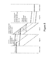
- Figure 5 illustrates energy density due to onset of Fowler-Nordheim tunneling.
- Figure 6 shows a calculation of the density of states (DOS) of Li 3 PO 4 and Li 3 PO 4-x N x that shows that these materials.
- Figure 7 shows one version of the devices that includes electrodes and multiple layers of dielectric material separated by layers of blocking material.
- Figure 8 illustrates a device 800 that includes first and second electrodes, a dielectric layer disposed between them, and first and second blocking layers.
- Figure 9 illustrates breakdown voltage of energy storage devices.
- Figure 10 is a graph illustrating performance of an exemplary energy storage device with SiO 2 as dielectric material and PZT as blocking material according to embodiments of the present invention.
- blocking layers are provided between dielectric material and the electrodes of an energy storage device.
- the block layers are characterized by higher dielectric constant than the dielectric material.
- Capacitive energy storage has well-known advantages versus electrochemical energy storage, e.g. in a battery. Compared to batteries, capacitors are able to store energy with very high power density, i.e. charge/recharge rates, have long shelf life with little degradation, and can be charged and discharged (cycled) hundreds of thousands or millions of times. However, capacitors often do not store energy in as little volume or weight as in a battery, or at low cost per energy stored, making capacitors impractical for applications such as in electric vehicles. Accordingly, it would be an advance in energy storage technology to provide a capacitive energy storage capable of storing energy more densely per volume and/or mass.
- FIG 2 shows exemplary current voltage curves for a capacitive energy storage device.
- V the voltage across the electrodes
- Q the charge stored on the electrodes
- V max the maximum voltage
- Total Energy ⁇ 0 Qmax ⁇ V Q d Q
- the capacitance, C is equal to the area of electrodes, A, times the permittivity, ⁇ , of the dielectric material divided by the distance between the electrodes, d.
- the energy density of a device may be increased by increasing the permittivity of the dielectric material and/or by increasing the maximum field sustainable in the dielectric material.
- Capacitive energy storage has been limited by the relatively low field strengths sustainable in conventional high permittivity dielectric materials as shown in Figure 3 , which shows the permittivity and breakdown field strength of a number of common dielectrics.
- the dotted line on Figure 3 indicates that the energy density of standard dielectric materials is limited to about 3 Wh/L.
- FIG. 4 shows one version of a high energy density energy storage device described herein.
- the device (400) includes first and second electrodes (410 & 420) spaced apart and a dielectric layer (430) disposed between the electrodes.
- the device also includes blocking layer (440) disposed between the first electrode and the dielectric layer and blocking layer (450) disposed between the second electrode and the dielectric layer.
- the blocking layers, 440 and 450 are made of materials with higher dielectric constant than that of the material of the dielectric layer.
- the blocking layers, 440 and 450 may be the same material or may be different materials.
- the dielectric layer is also referred to as the "low-k material” and the blocking layers is also referred to as the "high-k material.”
- the designations "high” and “low” indicate the relative magnitudes of the dielectric constants of the materials not their absolute values.
- the structure shown in Figure 4 has increased breakdown tolerance, and hence higher energy density, because of the suppression by the blocking layers of injection of charge carriers from the electrodes into the dielectric material.
- this device may have high energy density because the onset of Fowler-Nordheim (FN) tunneling from the electrodes into the dielectric material is delayed to higher voltages.
- the delay of FN tunneling results from the scarcity of charge carriers at the low-k material interface.
- Figure 5 shows that the area B is larger than area A. Tunneling probability of an electron at the interface is inversely related exponentially to the area under the potential barrier (from the WKB approximation).
- the area B will be larger, and the probability of detrimental electron tunneling is exponentially lower.
- the double layer has a charge that repels electrons FN tunneling will be further suppressed.
- the leftmost high-k layer in the example above has anion conduction, the anions will create a double layer at the high-k/low-k interface, and this negative charge will repel electrons from this interface.
- the dielectric layer may generally be made of any dielectric material.
- the dielectric layer material has a breakdown field strength of greater than 0.5V/nm. Breakdown field strength is determined by (i) placing a layer of about 50nm thickness of the test material between conductive electrodes one of which is approximately circular with a diameter of 100 ⁇ m and the other of which is larger than the 100 ⁇ m electrode; (ii) applying a linear voltage ramp across the electrodes, ramping up from 0V at a rate of about 0.1V/s; and, (iii) measuring the current flowing between the electrodes as a function of applied voltage. The breakdown voltage is measured at approximately room temperature.
- a typical current-voltage plot is presented in Figure 9 , showing an initial low voltage region (910) and a breakdown region (920).
- the breakdown voltage is calculated as the voltage at which the current is ten times the measured capacitive charging current.
- the capacitive charging current is 10 -10 A
- the breakdown voltage is about 1V (940) at which the current is 10 -9 A.
- the breakdown field strength is calcualted as the breakdown voltage divided by the thickness of the test material, which may be measured by cross-sectional TEM, X-ray reflectometry (XRR) or elipsometry.
- the current fluctuations shown at about 0.8 V (930) are typical of such current-voltage plots and are seen at voltages approaching the breakdown voltage.
- the dielectric layer material has a relative permittivity of less than 15.
- the relative permittivity is measured at approximately room temperature.
- the dielectric layer material has a band gap of greater than 4eV.
- the breakdown field strength, relative permittivity and band gap described in this parapgraph are material properties of the material that may be used for the dielectric layer; they are not the material properties of the composite blocking layer/dielectric layer/blocking layer system.
- dielectric layer materials that may be used include SiO 2 , HfO 2 , Al 2 O 3 , Si 3 N 4 , oxides, nitrides, oxynitrides and fluorides.
- the dielectric layer material is SiO 2 , HfO 2 , Al 2 O 3 or S 13 N 4 .
- the blocking layer may generally be made of any material having a dielectric constant greater than that of the dielectric constant of the dielectric layer material.
- the blocking layer material has a breakdown field strength of between 1mV/nm and 200mV/nm.
- the blocking layer material has a relative permittivity of greater than 100.
- the blocking layer material has a band gap of less than 4eV.
- the blocking layer material is ionically conducting, has an relative permittivity of greater than 100 and a band gap of greater than 3eV.
- the breakdown field strength, relative permittivity and band gap described in this paragraph are material properties of the material that may be used for the bloxking layer; they are not the material properties of the composite blocking layer/dielectric layer/blocking layer system.
- the blocking layer material may be an ionically conducting material or a non-ionically conducting material.
- the material derives its permittivity at least in part from ion migration within the material, establishing double layers at each interface. These double layers may be engineered to further deplete the electron concentration at the interface to delay the onset of FN tunneling, as is described in Figure 5 .
- the ionically conducting material is an anion conductor.
- the ionically conducting material is a cation conductor.
- the ionically conducting material is a Li + , H + , Na + , O 2- or F - conductor.
- the ionically conducting material is a Li + ion conductor.
- the ionically conducting material Li 3 PO 4 or Li 3 PO 4-x N x As used in this patent application, LiPON means Li 3 PO 4-x N x .
- Figure 6 shows a calculation of the density of states (DOS) of Li 3 PO 4 and Li 3 PO 4-x N x that shows that these materials, along with having a high relative permittivity, have a high bandgap, further delaying the onset of FN tunneling.
- the first blocking layer is an anion conducting material and the second blocking layer is a cation conducting material.
- one or both of the blocking layers comprises an anion conducting material and a cation conducting material.
- a device (800) includes first and second electrodes (810 & 820), a dielectric layer (830) disposed between them and first and second blocking layers (840 & 850) disposed between the dielectric layer and the first and second electrodes respectively.
- the first and second blocking layers include anion conducting material (860 & 880) and cation conducting material (870 & 890).
- only one of the first or second blocking layers includes both cation and anion conducting materials and the other blocking layer includes either a non-ionically conducting material or a cation or anion conducting material.
- the anion conducting material is proximate to the electrode and in other versions of the devices the cation conducting material is proximate to the electrode.
- the material derives its permittivity at least in part from the intrinsic polarizability of the material.
- the non-ionically conducting material is a high-k ceramic material.
- the non-ionically conducting material is a ferroelectric perovskite.
- the non-ionically conducting material is PZT (Pb(Zr 0.5 Ti 0.5 )O 3 ).
- the non-ionically conducting material is SrTiO 3 , PbTiO 3 , BaTiO 3 or (BaSr)TiO 3 .
- the non-ionically conducting material is a multiferroic high k material.
- the non-ionically conducting material is CaCu 3 Ti 4 O 12 or La 2-x Sr x NiO 4 .
- the non-ionically conducting material is a nanocomposite high-k material.
- the blocking layer material has a higher dielectric constant than that of the dielectric layer material.
- the dielectric constant of the blocking layer rmaterial is between 10 and 10000 times greater than the dielectric constant of the dielectric layer rmaterial. In another version the dielectric constant of the blocking layer rmaterial is between 100 and 1000 times greater than the dielectric constant of the dielectric layer rmaterial.
- the electrodes may generally be made of any conducting material that is compatible with the materials of the device with which they have contact.
- the electrodes may, independently, be made of Pt, Cu, Al, Ag or Au.
- the eletrodes may be of the same or different materials.
- the eletrodes have different work functions.
- the electrode that is positively biased during charge has a work function that is lower than that of the work function of the electrode that is negatively biased during charge.
- the electrode that is positively biased during charge has a work function of less than 4.5eV.
- the electrode that is negatively biased during charge has a work function of greater than 4.0eV.
- the blocking layer may generally be of any thickness that maintains the charge carrier injection supression function of the layer. In one version the blocking layer has a thickness of between 4 nm and 100 nm.
- the dielectric layer may generally be of any thickness that maximizes energy storage density while maintaining an insulating property under high field. In one version the dielectric layer has a thickness of between 20 nm and 10 ⁇ m. As shown in the calculation below it may be advantageous for the dielectric layer to be thicker than the blocking layers. In one version the dielectric layer is between 1 and 1000 times the thickness of the blocking layer.
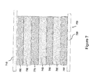
- Figure 7 shows one version of the devices that includes electrodes 710 and 720 and multiple layers of dielectric material (730, 740, 750) separated by layers of blocking material (760, 770, 780, 790).
- Laminate devices In one version of the devices, the dielectric and blocking layers are laminate layers in direct contact with each other with the architectures shown in Figures 4 , 7 and 8 and as otherwise described herein. In other versions the devices include one or more interfacial layers between one or more of the electrodes, dielectric layer and blocking layers.
- a device as described herein has an energy density of between 5 and 1000 Whr/kg. In another version a device as described herein has an energy density of between 10 and 650 Whr/kg. In another version a device as described herein has an energy density of between 50 and 500 Whr/kg. In another version a device as described herein has an energy density of greater than 50 Whr/kg. As used herein, energy density if the energy density at the device level; i.e., the total energy stored in the device divided by the mass of the device.
- the devices described herein may be fabricated in a number of ways, for example using sputtering, PVD, ALD or CVD.
- the devices are fabricated by sputtering using an Endura 5500, 200mm by Applied Materials.
- laminate devices are fabricated by sequential deposition of the blocking layers, dielectric layer(s) and electrodes on a substrate.
- a substrate is not required and the blocking layers, dielectric layer(s) and electrode layer(s) may be deposited directly on to one of the electrodes.
- the devices described herein may generally be used in any application requiring energy storage.
- the devices may be particularly well suited for use in applications such as in electric vehicles, hybrid electric vehicles and grid storage and regulation.
- Devices may be made with the following dielectric and blocking layers
- the devices described herein may have high breakdown strength because a) FN tunneling is not dominant, (for example, calculations suggest that other failure mechanisms in SiO 2 limit the breakdown tolerance to ⁇ 20V/nm) b) the low-k material is intrinsically a high breakdown material (for example, because of high purity, low defect concentration, high bandgap, etc.) c) the electric field is dropped primarily in the low-k material, which has high breakdown strength d) by interleaving thin nano-layers of the low-k material with the high-k material, any free charge carriers in the conduction band may not gain sufficient kinetic energy to cause damage via impact ionization.
- the material under voltage stress may be advantageous for the material under voltage stress have a low defect concentration.
- Defects which introduce states in the middle of the band gap of the insulator can lead to breakdown of the insulator.
- One mechanism by which defects lead to breakdown is that as defects form in a capacitor near the electrode, the field gets concentrated around those defects, enhancing the current around those defects, which leads to heating (and ionization), which results in further defect creation, forming a positive feedback. In the laminate structure, this feedback between defects and current cannot occur, since the material adjacent to the (defective) insulator is not conducting.
- Figure 10 is a graph illustrating performance of an exemplary energy storage device with SiO 2 as dielectric material and PZT as blocking material according to embodiments of the present invention. The graph is generated under the following conditions:
- a stable and substantially uniform electric field is maintained at a about 0.48V/nm.
- the applied electric field is about 0.1.V/nm, and the energy density is about 0.23 Wh/l.
- the high ⁇ region has low field, and low ⁇ region has higher field.
- the applied electric field is 2.2V/nm, the energy density is at about 112Wh/l.
- the blocking layer is characterized by a thickness of 2 nm with 2 nm spacing.
- the applied energy is 0.1V/nm, the energy density is at about 0.095 Wh/l.
- the applied energy is 5.2V/nm, the energy density is at about 257 Wh/l.
- a conductive substrate, or an insulting substrate with a conductive coating forms a first electrode.
- Alternating dielectric and blocking materials are deposited by PVD, sputtering, evaporation, high rate evaporation, close space sublimation, CVD, ALD, PECVD, or solution synthesis such as CBD, precipitation, spray coating, spin coating, roll coating, slot-die, etc.
- SiO 2 may be deposited by sputtering in an Applied Materials Endura 200mm system by reactive RF sputtering of Si in an oxygen plasma.
- LiPON may be deposited in a similar fashion from a Li 3 PO 4 target in a nitrogen plasma.
- One or more stacks of dielectric/blocking layers may be alternated in turn.
- a top electrode may be deposited by a solution process, or a vacuum process, for instance one selected from the list provided above.
- the device may be packaged for reliability and to prevent ingress of oxygen or humidity by any number of techniques common in semiconductor packaging, for example, by alternating layers of parylene and titanium.
- the electrodes are fed through a hermetic seal as common in battery devices.
- any element in a claim that does not explicitly state "means for” performing a specified function, or “step for” performing a specific function, is not to be interpreted as a "means” or “step” clause as specified in 35 U.S.C. Section 112, Paragraph 6.
- the use of "step of” or “act of” in the Claims herein is not intended to invoke the provisions of 35 U.S.C. 112, Paragraph 6.
Landscapes
- Engineering & Computer Science (AREA)
- Power Engineering (AREA)
- Chemical & Material Sciences (AREA)
- Manufacturing & Machinery (AREA)
- Microelectronics & Electronic Packaging (AREA)
- Ceramic Engineering (AREA)
- Inorganic Chemistry (AREA)
- Secondary Cells (AREA)
- Fixed Capacitors And Capacitor Manufacturing Machines (AREA)
Applications Claiming Priority (1)
| Application Number | Priority Date | Filing Date | Title |
|---|---|---|---|
| US201261592517P | 2012-01-30 | 2012-01-30 |
Publications (1)
| Publication Number | Publication Date |
|---|---|
| EP2620962A1 true EP2620962A1 (en) | 2013-07-31 |
Family
ID=47750419
Family Applications (1)
| Application Number | Title | Priority Date | Filing Date |
|---|---|---|---|
| EP20130153146 Withdrawn EP2620962A1 (en) | 2012-01-30 | 2013-01-29 | Solid state energy storage devices |
Country Status (3)
| Country | Link |
|---|---|
| US (2) | US9087645B2 (zh) |
| EP (1) | EP2620962A1 (zh) |
| CN (1) | CN103227048B (zh) |
Cited By (1)
| Publication number | Priority date | Publication date | Assignee | Title |
|---|---|---|---|---|
| EP3549189A4 (en) * | 2016-12-02 | 2019-11-20 | Capacitor Sciences Incorporated | MULTILAYER ELECTRODE AND FILM ENERGY ACCUMULATION DEVICE |
Families Citing this family (24)
| Publication number | Priority date | Publication date | Assignee | Title |
|---|---|---|---|---|
| US9011627B2 (en) | 2007-10-05 | 2015-04-21 | Carver Scientific, Inc. | Method of manufacturing high permittivity low leakage capacitor and energy storing device |
| JP5358839B2 (ja) | 2007-10-05 | 2013-12-04 | カーバー サイエンティフィック,インコーポレイテッド | 高誘電率低漏洩キャパシタおよびエネルギー蓄積デバイス、ならびにそれらを作製するための方法 |
| US8940850B2 (en) | 2012-08-30 | 2015-01-27 | Carver Scientific, Inc. | Energy storage device |
| US10056609B2 (en) | 2011-07-11 | 2018-08-21 | Quantumscape Corporation | Solid state energy storage devices |
| US9087645B2 (en) | 2012-01-30 | 2015-07-21 | QuantrumScape Corporation | Solid state energy storage devices |
| US10199165B2 (en) | 2012-08-30 | 2019-02-05 | Carver Scientific, Inc. | Energy storage device |
| US9805869B2 (en) | 2012-11-07 | 2017-10-31 | Carver Scientific, Inc. | High energy density electrostatic capacitor |
| SG11201609438UA (en) | 2014-05-12 | 2016-12-29 | Capacitor Sciences Inc | Capacitor and method of production thereof |
| US10340082B2 (en) | 2015-05-12 | 2019-07-02 | Capacitor Sciences Incorporated | Capacitor and method of production thereof |
| AU2015259291A1 (en) | 2014-05-12 | 2016-11-24 | Capacitor Sciences Incorporated | Energy storage device and method of production thereof |
| US10347423B2 (en) | 2014-05-12 | 2019-07-09 | Capacitor Sciences Incorporated | Solid multilayer structure as semiproduct for meta-capacitor |
| WO2016073522A1 (en) | 2014-11-04 | 2016-05-12 | Capacitor Sciences Incorporated | Energy storage devices and methods of production thereof |
| SG11201706689QA (en) | 2015-02-26 | 2017-09-28 | Capacitor Sciences Inc | Self-healing capacitor and methods of production thereof |
| US9932358B2 (en) | 2015-05-21 | 2018-04-03 | Capacitor Science Incorporated | Energy storage molecular material, crystal dielectric layer and capacitor |
| US9941051B2 (en) | 2015-06-26 | 2018-04-10 | Capactor Sciences Incorporated | Coiled capacitor |
| US10026553B2 (en) | 2015-10-21 | 2018-07-17 | Capacitor Sciences Incorporated | Organic compound, crystal dielectric layer and capacitor |
| US10305295B2 (en) | 2016-02-12 | 2019-05-28 | Capacitor Sciences Incorporated | Energy storage cell, capacitive energy storage module, and capacitive energy storage system |
| US11095129B2 (en) * | 2016-02-12 | 2021-08-17 | Capacitor Sciences Incorporated | Capacitor based power system and unmanned vehicle with the capacitor based power system thereof |
| US10153087B2 (en) | 2016-04-04 | 2018-12-11 | Capacitor Sciences Incorporated | Electro-polarizable compound and capacitor |
| US9978517B2 (en) | 2016-04-04 | 2018-05-22 | Capacitor Sciences Incorporated | Electro-polarizable compound and capacitor |
| AU2017367692B2 (en) | 2016-12-02 | 2022-04-14 | Carver Scientific, Inc. | Memory device and capacitive energy storage device |
| KR102627292B1 (ko) | 2018-03-12 | 2024-01-19 | 오메가 에너지 시스템스, 엘엘씨 | 전이 금속 아산화물의 고체-상태 에너지 수확기 |
| WO2021097051A1 (en) | 2019-11-13 | 2021-05-20 | Omega Energy Systems, Llc | Three-electrode solid-state energy harvester of transition metal suboxides |
| CN112080732B (zh) * | 2020-07-29 | 2021-12-28 | 西安交通大学 | 一种硅集成的bt-bmz薄膜、电容器及其制造方法 |
Citations (3)
| Publication number | Priority date | Publication date | Assignee | Title |
|---|---|---|---|---|
| US20050161717A1 (en) * | 2004-01-28 | 2005-07-28 | Fujitsu Limited | Semiconductor device and method of fabricating the same |
| US20080160712A1 (en) * | 2006-12-27 | 2008-07-03 | Hynix Semiconductor Inc. | Multiple-layer dielectric layer and method for fabricating capacitor including the same |
| US20080277761A1 (en) * | 2007-05-08 | 2008-11-13 | Texas Instruments, Inc. | On-chip isolation capacitors, circuits therefrom, and methods for forming the same |
Family Cites Families (20)
| Publication number | Priority date | Publication date | Assignee | Title |
|---|---|---|---|---|
| CA849697A (en) * | 1970-08-18 | General Electric Company | Capacitor with ionic conducting ceramic electrolyte | |
| FR2601812B1 (fr) | 1986-07-21 | 1988-11-25 | Atesys Sa | Condensateur electrique pour temperatures elevees |
| US5471364A (en) * | 1993-03-31 | 1995-11-28 | Texas Instruments Incorporated | Electrode interface for high-dielectric-constant materials |
| US5905000A (en) | 1996-09-03 | 1999-05-18 | Nanomaterials Research Corporation | Nanostructured ion conducting solid electrolytes |
| JP2002075783A (ja) * | 2000-08-25 | 2002-03-15 | Alps Electric Co Ltd | 温度補償用薄膜コンデンサ |
| JPWO2002065573A1 (ja) * | 2001-02-15 | 2004-06-17 | 松下電器産業株式会社 | 固体電解質電池およびその製造方法 |
| KR100541551B1 (ko) * | 2003-09-19 | 2006-01-10 | 삼성전자주식회사 | 적어도 3층의 고유전막들을 갖는 아날로그 커패시터 및그것을 제조하는 방법 |
| WO2006124670A2 (en) * | 2005-05-12 | 2006-11-23 | Georgia Tech Research Corporation | Coated metal oxide nanoparticles and methods for producing same |
| US7643714B2 (en) | 2005-06-28 | 2010-01-05 | California Institute Of Technology | Nanophotonic devices in silicon |
| US8377586B2 (en) * | 2005-10-05 | 2013-02-19 | California Institute Of Technology | Fluoride ion electrochemical cell |
| US7532083B2 (en) | 2006-03-23 | 2009-05-12 | Intel Corporation | Active nonlinear transmission line |
| US7830644B2 (en) * | 2007-03-05 | 2010-11-09 | Northop Grumman Systems Corporation | High dielectric capacitor materials and method of their production |
| US20110110015A1 (en) * | 2007-04-11 | 2011-05-12 | The Penn State Research Foundation | Methods to improve the efficiency and reduce the energy losses in high energy density capacitor films and articles comprising the same |
| KR20090051634A (ko) * | 2007-11-19 | 2009-05-22 | 삼성전자주식회사 | 캐패시터 및 그 제조 방법 |
| US20110275005A1 (en) | 2008-10-24 | 2011-11-10 | Nanosys, Inc | Membrane Electrode Assemblies With Interfacial Layer |
| CN102282646A (zh) | 2009-01-16 | 2011-12-14 | 利兰·斯坦福青年大学托管委员会 | 量子点超级电容器和电子电池 |
| US10056609B2 (en) | 2011-07-11 | 2018-08-21 | Quantumscape Corporation | Solid state energy storage devices |
| US8541282B2 (en) * | 2011-11-07 | 2013-09-24 | Intermolecular, Inc. | Blocking layers for leakage current reduction in DRAM devices |
| US20130143087A1 (en) * | 2011-12-01 | 2013-06-06 | Applied Nanostructured Solutions, Llc. | Core/shell structured electrodes for energy storage devices |
| US9087645B2 (en) | 2012-01-30 | 2015-07-21 | QuantrumScape Corporation | Solid state energy storage devices |
-
2013
- 2013-01-25 US US13/749,706 patent/US9087645B2/en active Active
- 2013-01-29 CN CN201310034515.9A patent/CN103227048B/zh active Active
- 2013-01-29 EP EP20130153146 patent/EP2620962A1/en not_active Withdrawn
-
2015
- 2015-04-29 US US14/700,048 patent/US9293255B2/en active Active
Patent Citations (3)
| Publication number | Priority date | Publication date | Assignee | Title |
|---|---|---|---|---|
| US20050161717A1 (en) * | 2004-01-28 | 2005-07-28 | Fujitsu Limited | Semiconductor device and method of fabricating the same |
| US20080160712A1 (en) * | 2006-12-27 | 2008-07-03 | Hynix Semiconductor Inc. | Multiple-layer dielectric layer and method for fabricating capacitor including the same |
| US20080277761A1 (en) * | 2007-05-08 | 2008-11-13 | Texas Instruments, Inc. | On-chip isolation capacitors, circuits therefrom, and methods for forming the same |
Cited By (1)
| Publication number | Priority date | Publication date | Assignee | Title |
|---|---|---|---|---|
| EP3549189A4 (en) * | 2016-12-02 | 2019-11-20 | Capacitor Sciences Incorporated | MULTILAYER ELECTRODE AND FILM ENERGY ACCUMULATION DEVICE |
Also Published As
| Publication number | Publication date |
|---|---|
| US9087645B2 (en) | 2015-07-21 |
| US20130194716A1 (en) | 2013-08-01 |
| US9293255B2 (en) | 2016-03-22 |
| US20150235768A1 (en) | 2015-08-20 |
| CN103227048B (zh) | 2017-06-23 |
| CN103227048A (zh) | 2013-07-31 |
Similar Documents
| Publication | Publication Date | Title |
|---|---|---|
| US9293255B2 (en) | Solid state energy storage devices | |
| US9646766B2 (en) | Method of making dielectric capacitors with increased dielectric breakdown strength | |
| US10741334B2 (en) | Method and associated capacitors having engineered electrodes with very high energy density | |
| US9178006B2 (en) | Methods to improve electrical performance of ZrO2 based high-K dielectric materials for DRAM applications | |
| US9111681B2 (en) | Thin film capacitor | |
| US11145665B2 (en) | Electrical storage device with negative capacitance | |
| US20070121274A1 (en) | Small volume thin film and high energy density crystal capacitors | |
| US8481384B2 (en) | Method for producing MIM capacitors with high K dielectric materials and non-noble electrodes | |
| US7084482B2 (en) | Capacitor of a semiconductor device and memory device using the same | |
| CN113168932B (zh) | 利用真空或气体进行电绝缘的电介质结构 | |
| US11417724B2 (en) | Capacitor including perovskite material, semiconductor device including the capacitor, and method of manufacturing the capacitor | |
| CN116458282A (zh) | 用于金属-绝缘体-金属电容器的四层高k | |
| US10446324B2 (en) | Thin film capacitor | |
| Smitha et al. | Annealing effects on capacitance density and voltage coefficient of capacitance (VCC) of thin-film capacitor for energy harvesting application | |
| WO2022219939A1 (ja) | キャパシタ、電気回路、回路基板、電子機器、及び蓄電デバイス | |
| US20200027660A1 (en) | Multilayer capacitor | |
| US20060170073A1 (en) | Capacitor with high breakdown field | |
| US20230207201A1 (en) | Dielectric composition and multilayer capacitor | |
| US20230215635A1 (en) | Dielectric composition and multilayer capacitor | |
| Park et al. | Electrical Charateristics of ZrO₂-Al₂O₃-ZrO₂ Laminated Capacitor via Changes of Bottom Electrode-Alumina Distances | |
| Sahoo et al. | ZrO2 Layer Thickness and Field Dependent Leakage Current in Ba0. 8Sr0. 2TiO3/ZrO2 Heterostructured Thin Films |
Legal Events
| Date | Code | Title | Description |
|---|---|---|---|
| PUAI | Public reference made under article 153(3) epc to a published international application that has entered the european phase |
Free format text: ORIGINAL CODE: 0009012 |
|
| AK | Designated contracting states |
Kind code of ref document: A1 Designated state(s): AL AT BE BG CH CY CZ DE DK EE ES FI FR GB GR HR HU IE IS IT LI LT LU LV MC MK MT NL NO PL PT RO RS SE SI SK SM TR |
|
| AX | Request for extension of the european patent |
Extension state: BA ME |
|
| 17P | Request for examination filed |
Effective date: 20131210 |
|
| RBV | Designated contracting states (corrected) |
Designated state(s): AL AT BE BG CH CY CZ DE DK EE ES FI FR GB GR HR HU IE IS IT LI LT LU LV MC MK MT NL NO PL PT RO RS SE SI SK SM TR |
|
| 17Q | First examination report despatched |
Effective date: 20140515 |
|
| STAA | Information on the status of an ep patent application or granted ep patent |
Free format text: STATUS: EXAMINATION IS IN PROGRESS |
|
| STAA | Information on the status of an ep patent application or granted ep patent |
Free format text: STATUS: THE APPLICATION IS DEEMED TO BE WITHDRAWN |
|
| 18D | Application deemed to be withdrawn |
Effective date: 20170124 |