EP2615637A2 - Semiconductor package and method for manufacturing the same - Google Patents
Semiconductor package and method for manufacturing the same Download PDFInfo
- Publication number
- EP2615637A2 EP2615637A2 EP13000145.6A EP13000145A EP2615637A2 EP 2615637 A2 EP2615637 A2 EP 2615637A2 EP 13000145 A EP13000145 A EP 13000145A EP 2615637 A2 EP2615637 A2 EP 2615637A2
- Authority
- EP
- European Patent Office
- Prior art keywords
- semiconductor device
- straight line
- positioning pattern
- semiconductor
- substrate
- Prior art date
- Legal status (The legal status is an assumption and is not a legal conclusion. Google has not performed a legal analysis and makes no representation as to the accuracy of the status listed.)
- Granted
Links
Images


Classifications
-
- H—ELECTRICITY
- H10—SEMICONDUCTOR DEVICES; ELECTRIC SOLID-STATE DEVICES NOT OTHERWISE PROVIDED FOR
- H10W—GENERIC PACKAGES, INTERCONNECTIONS, CONNECTORS OR OTHER CONSTRUCTIONAL DETAILS OF DEVICES COVERED BY CLASS H10
- H10W46/00—Marks applied to devices, e.g. for alignment or identification
-
- H—ELECTRICITY
- H10—SEMICONDUCTOR DEVICES; ELECTRIC SOLID-STATE DEVICES NOT OTHERWISE PROVIDED FOR
- H10W—GENERIC PACKAGES, INTERCONNECTIONS, CONNECTORS OR OTHER CONSTRUCTIONAL DETAILS OF DEVICES COVERED BY CLASS H10
- H10W70/00—Package substrates; Interposers; Redistribution layers [RDL]
- H10W70/60—Insulating or insulated package substrates; Interposers; Redistribution layers
- H10W70/62—Insulating or insulated package substrates; Interposers; Redistribution layers characterised by their interconnections
- H10W70/65—Shapes or dispositions of interconnections
-
- H—ELECTRICITY
- H10—SEMICONDUCTOR DEVICES; ELECTRIC SOLID-STATE DEVICES NOT OTHERWISE PROVIDED FOR
- H10W—GENERIC PACKAGES, INTERCONNECTIONS, CONNECTORS OR OTHER CONSTRUCTIONAL DETAILS OF DEVICES COVERED BY CLASS H10
- H10W46/00—Marks applied to devices, e.g. for alignment or identification
- H10W46/101—Marks applied to devices, e.g. for alignment or identification characterised by the type of information, e.g. logos or symbols
-
- H—ELECTRICITY
- H10—SEMICONDUCTOR DEVICES; ELECTRIC SOLID-STATE DEVICES NOT OTHERWISE PROVIDED FOR
- H10W—GENERIC PACKAGES, INTERCONNECTIONS, CONNECTORS OR OTHER CONSTRUCTIONAL DETAILS OF DEVICES COVERED BY CLASS H10
- H10W46/00—Marks applied to devices, e.g. for alignment or identification
- H10W46/301—Marks applied to devices, e.g. for alignment or identification for alignment
-
- H—ELECTRICITY
- H10—SEMICONDUCTOR DEVICES; ELECTRIC SOLID-STATE DEVICES NOT OTHERWISE PROVIDED FOR
- H10W—GENERIC PACKAGES, INTERCONNECTIONS, CONNECTORS OR OTHER CONSTRUCTIONAL DETAILS OF DEVICES COVERED BY CLASS H10
- H10W46/00—Marks applied to devices, e.g. for alignment or identification
- H10W46/601—Marks applied to devices, e.g. for alignment or identification for use after dicing
- H10W46/607—Located on parts of packages, e.g. on encapsulations or on package substrates
-
- H—ELECTRICITY
- H10—SEMICONDUCTOR DEVICES; ELECTRIC SOLID-STATE DEVICES NOT OTHERWISE PROVIDED FOR
- H10W—GENERIC PACKAGES, INTERCONNECTIONS, CONNECTORS OR OTHER CONSTRUCTIONAL DETAILS OF DEVICES COVERED BY CLASS H10
- H10W72/00—Interconnections or connectors in packages
- H10W72/071—Connecting or disconnecting
- H10W72/073—Connecting or disconnecting of die-attach connectors
-
- H—ELECTRICITY
- H10—SEMICONDUCTOR DEVICES; ELECTRIC SOLID-STATE DEVICES NOT OTHERWISE PROVIDED FOR
- H10W—GENERIC PACKAGES, INTERCONNECTIONS, CONNECTORS OR OTHER CONSTRUCTIONAL DETAILS OF DEVICES COVERED BY CLASS H10
- H10W72/00—Interconnections or connectors in packages
- H10W72/071—Connecting or disconnecting
- H10W72/073—Connecting or disconnecting of die-attach connectors
- H10W72/07321—Aligning
- H10W72/07327—Aligning involving guiding structures, e.g. spacers or supporting members
-
- H—ELECTRICITY
- H10—SEMICONDUCTOR DEVICES; ELECTRIC SOLID-STATE DEVICES NOT OTHERWISE PROVIDED FOR
- H10W—GENERIC PACKAGES, INTERCONNECTIONS, CONNECTORS OR OTHER CONSTRUCTIONAL DETAILS OF DEVICES COVERED BY CLASS H10
- H10W72/00—Interconnections or connectors in packages
- H10W72/071—Connecting or disconnecting
- H10W72/075—Connecting or disconnecting of bond wires
-
- H—ELECTRICITY
- H10—SEMICONDUCTOR DEVICES; ELECTRIC SOLID-STATE DEVICES NOT OTHERWISE PROVIDED FOR
- H10W—GENERIC PACKAGES, INTERCONNECTIONS, CONNECTORS OR OTHER CONSTRUCTIONAL DETAILS OF DEVICES COVERED BY CLASS H10
- H10W72/00—Interconnections or connectors in packages
- H10W72/30—Die-attach connectors
- H10W72/351—Materials of die-attach connectors
- H10W72/353—Materials of die-attach connectors not comprising solid metals or solid metalloids, e.g. ceramics
- H10W72/354—Materials of die-attach connectors not comprising solid metals or solid metalloids, e.g. ceramics comprising polymers
-
- H—ELECTRICITY
- H10—SEMICONDUCTOR DEVICES; ELECTRIC SOLID-STATE DEVICES NOT OTHERWISE PROVIDED FOR
- H10W—GENERIC PACKAGES, INTERCONNECTIONS, CONNECTORS OR OTHER CONSTRUCTIONAL DETAILS OF DEVICES COVERED BY CLASS H10
- H10W72/00—Interconnections or connectors in packages
- H10W72/30—Die-attach connectors
- H10W72/381—Auxiliary members
- H10W72/385—Alignment aids, e.g. alignment marks
-
- H—ELECTRICITY
- H10—SEMICONDUCTOR DEVICES; ELECTRIC SOLID-STATE DEVICES NOT OTHERWISE PROVIDED FOR
- H10W—GENERIC PACKAGES, INTERCONNECTIONS, CONNECTORS OR OTHER CONSTRUCTIONAL DETAILS OF DEVICES COVERED BY CLASS H10
- H10W72/00—Interconnections or connectors in packages
- H10W72/30—Die-attach connectors
- H10W72/381—Auxiliary members
- H10W72/387—Flow barriers
-
- H—ELECTRICITY
- H10—SEMICONDUCTOR DEVICES; ELECTRIC SOLID-STATE DEVICES NOT OTHERWISE PROVIDED FOR
- H10W—GENERIC PACKAGES, INTERCONNECTIONS, CONNECTORS OR OTHER CONSTRUCTIONAL DETAILS OF DEVICES COVERED BY CLASS H10
- H10W72/00—Interconnections or connectors in packages
- H10W72/50—Bond wires
- H10W72/59—Bond pads specially adapted therefor
-
- H—ELECTRICITY
- H10—SEMICONDUCTOR DEVICES; ELECTRIC SOLID-STATE DEVICES NOT OTHERWISE PROVIDED FOR
- H10W—GENERIC PACKAGES, INTERCONNECTIONS, CONNECTORS OR OTHER CONSTRUCTIONAL DETAILS OF DEVICES COVERED BY CLASS H10
- H10W72/00—Interconnections or connectors in packages
- H10W72/851—Dispositions of multiple connectors or interconnections
- H10W72/874—On different surfaces
- H10W72/884—Die-attach connectors and bond wires
-
- H—ELECTRICITY
- H10—SEMICONDUCTOR DEVICES; ELECTRIC SOLID-STATE DEVICES NOT OTHERWISE PROVIDED FOR
- H10W—GENERIC PACKAGES, INTERCONNECTIONS, CONNECTORS OR OTHER CONSTRUCTIONAL DETAILS OF DEVICES COVERED BY CLASS H10
- H10W72/00—Interconnections or connectors in packages
- H10W72/90—Bond pads, in general
- H10W72/941—Dispositions of bond pads
- H10W72/944—Dispositions of multiple bond pads
- H10W72/9445—Top-view layouts, e.g. mirror arrays
-
- H—ELECTRICITY
- H10—SEMICONDUCTOR DEVICES; ELECTRIC SOLID-STATE DEVICES NOT OTHERWISE PROVIDED FOR
- H10W—GENERIC PACKAGES, INTERCONNECTIONS, CONNECTORS OR OTHER CONSTRUCTIONAL DETAILS OF DEVICES COVERED BY CLASS H10
- H10W90/00—Package configurations
- H10W90/701—Package configurations characterised by the relative positions of pads or connectors relative to package parts
- H10W90/731—Package configurations characterised by the relative positions of pads or connectors relative to package parts of die-attach connectors
- H10W90/734—Package configurations characterised by the relative positions of pads or connectors relative to package parts of die-attach connectors between a chip and a stacked insulating package substrate, interposer or RDL
-
- H—ELECTRICITY
- H10—SEMICONDUCTOR DEVICES; ELECTRIC SOLID-STATE DEVICES NOT OTHERWISE PROVIDED FOR
- H10W—GENERIC PACKAGES, INTERCONNECTIONS, CONNECTORS OR OTHER CONSTRUCTIONAL DETAILS OF DEVICES COVERED BY CLASS H10
- H10W90/00—Package configurations
- H10W90/701—Package configurations characterised by the relative positions of pads or connectors relative to package parts
- H10W90/751—Package configurations characterised by the relative positions of pads or connectors relative to package parts of bond wires
- H10W90/754—Package configurations characterised by the relative positions of pads or connectors relative to package parts of bond wires between a chip and a stacked insulating package substrate, interposer or RDL
Definitions
- the present invention relates to a semiconductor package that includes a semiconductor device and a substrate supporting the semiconductor device, and to a method for manufacturing the same.
- a wiring pattern of a foil such as copper is formed on a front surface of a substrate in a semiconductor package.
- a semiconductor device is then positioned and installed in a predetermined position on top of the substrate and terminals on the semiconductor device are directly connected or indirectly connected via bond wires to the wiring pattern on the substrate.
- the semiconductor device portion is sealed by a black resin (see, e.g., Related Art 1).
- a transparent resin such as a semiconductor package that includes an optical semiconductor device such as a light receiving element having a photodiode array for detecting optical displacement, for example.
- a position of the semiconductor device on the substrate affects a degree of accuracy for displacement detection. Therefore, highly accurate positioning of the semiconductor device on the substrate is required.
- a method for positioning and installing the semiconductor device on the substrate with a high degree of accuracy is known in which the semiconductor device is installed on the front surface of the substrate while correcting misalignment in positions and orientations of the substrate and the semiconductor device by detecting the position and orientation of each by capturing images of each with a camera (see, e.g., Related Art 2).
- an instrument such as a component placement system is necessary in order to detect and correct misalignment in the position and orientation of the substrate and the semiconductor device by capturing images of each with the camera.
- introduction of an instrument such as the component placement system is difficult from a cost perspective.
- chipping when the semiconductor device is split off from a semiconductor wafer, irregularly shaped breakages called chipping may be formed on an outer periphery (see, e.g., Related Art 3).
- chipping has formed on the outer periphery of the semiconductor device, detecting the position and orientation of the semiconductor device based on the shape of the outer periphery of the semiconductor device may lead to a reduction of accuracy in the detection of the position and orientation of the semiconductor device.
- a method in which a capture mark is formed on the substrate and the semiconductor device and the position and orientation of each is detected (see, e.g., Related Art 4).
- forming the capture mark may be difficult.
- the semiconductor device is the light receiving element having the photodiode array
- the region where the photodiode array is to be provided may overlap with the region where the capture mark is to be formed.
- forming the capture mark in a region other than the region where the capture mark is typically formed in order to not overlap with the region where the photodiode array is to be provided may lead to a reduction of accuracy in the detection of the position and orientation of the semiconductor device.
- a method is known in which a positioning hole or notch is formed in the semiconductor device and substrate, then the semiconductor device is positioned on the substrate by engaging a positioning jig to the positioning hole or notch (see, e.g., Related Arts 5 and 6).
- a method is known in which the semiconductor device is positioned on the substrate by mounting a positioning nub to the substrate and abutting the semiconductor device on this nub (see, e.g., Related Art 7).
- the hole or notch in order to increase accuracy in positioning of the semiconductor device, the hole or notch must be formed with a high degree of accuracy. In order to form such a highly accurate hole or notch, production time increases and costs increase.
- the positioning nub in order to increase accuracy in positioning of the semiconductor device, the positioning nub must be mounted to the substrate with a high degree of accuracy. In order to mount the positioning nub to the substrate with a high degree of accuracy, production time increases and costs increase.
- the present invention was conceived in light of the above-described circumstances and provides a semiconductor package and a method for manufacturing the same that is capable of achieving highly accurate positioning of a semiconductor device on a substrate at a low cost.
- the present invention resolves the above-described circumstances with a semiconductor package that includes a semiconductor device (also referred to as a "semiconductor") and a substrate, the semiconductor device having a straight line portion (also referred to as a "straight line segment") on an outer periphery and the substrate supporting the semiconductor device.
- a semiconductor package a foil positioning pattern is formed on a front surface of the substrate, the positioning pattern touching the straight line portion of the semiconductor device to regulate ( i.e ., set) a position of the semiconductor device.
- the present invention resolves the above-described circumstances with a method for manufacturing the semiconductor package that includes a pattern forming process and a semiconductor device installation process.
- the pattern forming process the foil positioning pattern for regulating the position of the semiconductor device is formed on the front surface of the substrate, which supports the semiconductor device having the straight line portion on the outer periphery thereof.
- the semiconductor device installation process the semiconductor device is installed on the front surface of the substrate while regulating the position of the semiconductor device by abutting the straight line portion of the semiconductor device on the positioning pattern.
- the foil positioning pattern can be formed with a high degree of accuracy on the front surface of the substrate in a process similar to a process for a foil wiring pattern.
- the semiconductor device By abutting the straight line portion of the semiconductor device on the positioning pattern, the semiconductor device can be positioned and installed on the front surface of the substrate with a high degree of accuracy. Accordingly, highly accurate positioning of the semiconductor device can be achieved at a low cost.
- a semiconductor package 10 includes a semiconductor device 14 and a substrate 16, the semiconductor device 14 having straight line portions on an outer periphery 12 and the substrate 16 supporting the semiconductor device 14.
- a foil positioning pattern 18 that touches the straight line portions of the semiconductor device 14 to regulate a position of the semiconductor device 14 is formed on a front surface of the substrate 16.
- Other structures are not considered particularly essential to an understanding of the present embodiment, and thus descriptions thereof are omitted as appropriate.
- the semiconductor device 14 is a light receiving element that includes a photodiode array for detecting optical displacement. More specifically, the semiconductor device 14 is rectangular and includes a first straight line portion 20A and a second straight line portion 20B on the outer periphery 12, the first straight line portion 20A and the second straight line portion 20B forming a right angle with respect to each other. Moreover, portions on the outer periphery 12 of the semiconductor device 14 that are related to the first straight line portion 20A and the second straight line portion 20B as an opposing side are also straight line portions. As shown in Fig. 1 , when the semiconductor device 14 is rectangular, a direction of the photodiode array (columnar direction of photodiodes) preferably matches a length direction of the semiconductor device 14.
- the semiconductor device 14 has a thickness in a range of approximately 0.05 to 0.7 mm.
- the thickness is appropriately selected in consideration of a manufacturing process cost, yield ratio, and the like for the semiconductor device.
- irregularly shaped breakages called chipping may be formed on the outer periphery 12, such as damage or peeling of a surface layer film.
- a portion on a bottom surface side of the outer periphery 12 may be missing.
- damage is preferably as small as possible. Processing requirements for the clipping process are considered such that a range where the damage occurs is less than 10 ⁇ m from a bottom surface.
- a material for the substrate 16 is a known material such as paper phenol, paper epoxy, glass composite, glass epoxy, Teflon (registered trademark), alumina, and LTCC.
- a material for the positioning pattern 18 is a foil such as copper foil and aluminum foil.
- the positioning pattern 18 has an "L" shape in a planar view.
- the positioning pattern 18 touches both the first straight line portion 20A and the second straight line portion 20B.
- the semiconductor device 14 is rectangular.
- the longer of the straight line portions of the positioning pattern 18 preferably touches the longer of the straight line portions of the semiconductor device 14 (the second straight line portion 20B).
- a notch 22 having a shape indented away from a corner of the semiconductor device 14 is formed on an interior corner of the L-shaped positioning pattern 18.
- the irregular breakage called chipping may form on the outer periphery 12 of the semiconductor device 14 as described above.
- a thickness A of the positioning pattern 18 is thinner than a height K from the bottom surface of a missing portion on the outer periphery 12 of the semiconductor device 14, as shown in Fig. 4 , the semiconductor device 14 abuts the positioning pattern 18 at the missing portion on the outer periphery 12, as shown in Fig. 5 .
- the semiconductor device 14 may also lift up on the positioning pattern 18, which accordingly becomes a cause of reduction in positioning accuracy for the semiconductor device 14.
- the semiconductor device 14 abuts the positioning pattern 18 at a portion of the outer periphery 12 where no damage has occurred, as shown in Fig. 8 , and thus the semiconductor device 14 can be accurately positioned on the substrate 16.
- a clipping process for semiconductor devices has been considered such that a range where damage to the outer periphery 12 of the semiconductor device 14 occurs is less than 10 ⁇ m from the bottom surface.
- the thickness of the positioning pattern 18 is 10 ⁇ m or greater, an undamaged portion of the outer periphery 12 of the semiconductor device 14 can reliably abut the positioning pattern 18. Accordingly, the thickness of the positioning pattern 18 is preferably 10 ⁇ m or greater. In addition, the thickness of the positioning pattern 18 is preferably thinner than the thickness of the semiconductor device 14. The thickness of the positioning pattern 18 is typically 18 ⁇ m, 35 ⁇ m, 70 ⁇ m, and the like.
- a foil wiring pattern 24 is also formed on the front surface of the substrate 16.
- the material and thickness for the wiring pattern 24 are the same as those for the positioning pattern 18.
- the wiring pattern 24 is connected to terminals of the semiconductor device 14 via bond wires 26.
- the semiconductor package 10 is sealed by a sealing resin 28 on a side where the semiconductor device 14 is installed on the substrate 16.
- a transparent epoxy-type resin for example, may be used as a material for the sealing resin 28.
- the foil positioning pattern 18 for regulating the position of the semiconductor device 14 is formed on the front surface of the substrate 16 (S102: pattern forming process).
- the wiring pattern 24 is also formed on the front surface of the substrate 16 in this process, the wiring pattern 24 having the same material and thickness as those of the positioning pattern 18 (see Fig. 3 ).
- foil such as copper foil is spread across the front surface of the substrate 16 and is processed into the shapes of the positioning pattern 18 and the wiring pattern 24 using a photolithography method.
- foil such as copper foil is also spread across the rear surface of the substrate 16 and is processed into the shape of the wiring pattern using the photolithography method.
- through-holes are formed in the substrate 16 so as to communicate with wirings on both surfaces.
- the through-holes are formed so as to be filled by plating in order to electrically connect the wiring patterns on both surfaces.
- the semiconductor device 14 is installed on the front surface of the substrate 16 while regulating the position of the semiconductor device 14 by abutting the first straight line portion 20A and the second straight line portion 20B of the semiconductor device 14 on the positioning pattern 18 (S104: semiconductor device installation process).
- S104 semiconductor device installation process
- an etching fillet is formed in the interior corner of the positioning pattern 18.
- the notch 22 is formed on the interior corner of the L-shaped positioning pattern 18, the notch 22 having a shape indented away from the corner of the semiconductor device 14. Therefore, as shown in Fig. 11 , the corner of the semiconductor device 14 and the interior corner of the L-shaped positioning pattern 18 do not interfere with each other. Accordingly, the first straight line portion 20A and the second straight line portion 20B of the semiconductor device 14 can reliably abut the positioning pattern 18 and accurate positioning of the semiconductor device 14 on the substrate 16 is possible.
- an adhesive of an epoxy resin or the like is applied to a plurality of locations (for example, five locations) on the contact surfaces of the substrate 16 and/or the semiconductor device 14.
- the terminals on the semiconductor device 14 and the wiring pattern 24 are connected via the bond wires 26.
- the side where the semiconductor device 14 has been installed on the substrate 16 is sealed by the sealing resin 28 (S106: resin sealing process).
- the semiconductor device 14 and the substrate 16 are installed in a mold of a resin molding apparatus such as a transfer molding apparatus.
- the side where the semiconductor device 14 has been installed on the substrate 16 is then sealed by the sealing resin 28 so as to cover the semiconductor device 14, thus completing the semiconductor package 10.
- the foil positioning pattern 18 can be formed with a high degree of accuracy on the front surface of the substrate 16 along with the foil wiring pattern 24 using a method such as lithography.
- the semiconductor device 14 can be positioned and installed on the front surface of the substrate 16 with a high degree of accuracy. Accordingly, with the semiconductor package 10, highly accurate positioning of the semiconductor device 14 can be achieved at a low cost.
- the notch 22 having a shape indented away from the corner of the semiconductor device 14 is formed on the interior corner of the L-shaped positioning pattern 18.
- the corner of the semiconductor device 14 has a chamfered shape and the corner of the semiconductor device 14 and the interior corner of the L-shaped positioning pattern 18 do not interfere with each other even when the etching fillet is formed on the interior corner of the L-shaped positioning pattern 18, for example, no notch need be formed on the interior corner of the L-shaped positioning pattern 18.
- a single (one) L-shaped positioning pattern 18 is formed on the front surface of the substrate 16 in the semiconductor package 10 of the first embodiment.
- a semiconductor package 30 in the present second embodiment includes a positioning pattern 32 formed on the front surface of the substrate 16, the positioning pattern 32 being divided into three positioning pattern elements 32A, 32B, and 32C.
- Other structures are similar to the first embodiment. Therefore, similar structures are given the same reference numerals as those in Figs. 1 to 11 and descriptions thereof are omitted.
- the positioning pattern 32 touches the first straight line portion 20A at the positioning pattern element 32A and touches the second straight line portion 20B at the positioning pattern elements 32B and 32C. More specifically, each of the positioning pattern elements 32A, 32B, and 32C are rectangular in a planar view.
- the positioning pattern element 32A touches the first straight line portion 20A at a portion away from an end portion of the first straight line portion 20A.
- the positioning pattern elements 32B and 32C touch end portions and portions near the end portions of the second straight line portion 20B.
- the positioning pattern elements 32B and 32C are separated in an extension direction of the second straight line portion 20B.
- a portion of the positioning pattern elements 32B and 32C projects in the extension direction of the second straight line portion 20B past the respective end portions of the second straight line portion 20B.
- the projecting portions do not touch the second straight line portion 20B.
- the material and thickness for the positioning pattern 32 are the same as those for the positioning pattern 18 and the wiring pattern 24.
- the positioning pattern 32 preferably touches two points on the longer of the straight line portions of the semiconductor device 14 (the second straight line portion 20B), the two points having a span that is as long as possible.
- the positioning pattern 32 more preferably touches both end portions of the longer of the straight line portions of the semiconductor device 14 (the second straight line portion 20B).
- the positioning pattern 32 of the semiconductor package 30 in the present second embodiment is also foil. Therefore, in the pattern forming process (S102), the positioning pattern 32 can be formed with a high degree of accuracy on the front surface of the substrate 16 along with the wiring pattern 24 using a method such as lithography. In addition, in the semiconductor device installation process (S104), the first straight line portion 20A of the semiconductor device 14 abuts the positioning pattern element 32A, and the second straight line portion 20B abuts the positioning pattern elements 32B and 32C. Thereby, the semiconductor device 14 can be positioned and installed on the front surface of the substrate 16 with a high degree of accuracy. Accordingly, highly accurate positioning of the semiconductor device 14 can be achieved at a low cost in the semiconductor package 30, as well.
- the excess adhesive 34 may spill over onto the semiconductor device 14 from between the first straight line portion 20A and the second straight line portion 20B of the semiconductor device 14 and the positioning pattern 32 and bond to the terminals of the semiconductor device 14.
- the positioning pattern elements 32B and 32C are separated in the extension direction of the second straight line portion 20B and, in addition, the positioning pattern elements 32A and 32B are separated. Therefore, the excess adhesive 34 can escape in a surface direction from between the positioning pattern elements 32B and 32C, or from between the positioning pattern elements 32A and 32B. Accordingly, a situation in which the excess adhesive 34 spills over onto the semiconductor device 14 and bonds to the terminals of the semiconductor device 14 is unlikely to occur.
- the portion of the L-shaped positioning pattern 18 touching the first straight line portion 20A and/or the portion touching the second straight line portion 20B may be separated (in the extension direction of the touching straight line portion) in the first embodiment, as well. Thereby, a situation in which the excess adhesive 34 spills over onto the semiconductor device 14 and bonds to the terminals of the semiconductor device 14 is unlikely to occur, similar to the present second embodiment.
- a third embodiment of the present invention is described.
- the positioning patterns 18 and 32 touch both the first straight line portion 20A and the second straight line portion 20B of the semiconductor device 14.
- a positioning pattern 42 touches only the second straight line portion 20B of the semiconductor device 14 and does not touch the first straight line portion 20A.
- positions of the end portions of the second straight line portion 20B and positions of end portions of the positioning pattern 42 are matched up.
- Other structures are similar to the first and second embodiments. Therefore, similar structures are given the same reference numerals as those in Figs. 1 to 14 and descriptions thereof are omitted.
- the positioning pattern 42 is configured with positioning pattern elements 42A and 42B, which are separated in the extension direction of the second straight line portion 20B. More specifically, the positioning pattern elements 42A and 42B are rectangular and touch end portions and portions near the end portions of the second straight line portion 20B.
- the position of the end portion of the positioning pattern element 42A matches up ( i.e ., aligns) with the position of a first end portion of the second straight line portion 20B.
- the position of the end portion of the positioning pattern element 42B matches up ( i.e ., aligns) with the position of a second end portion of the second straight line portion 20B.
- the material and thickness for the positioning pattern 42 are the same as those for the positioning pattern 18, the positioning pattern 32, and the wiring pattern 24.
- the positioning pattern 42 preferably touches the longer of the straight line portions of the semiconductor device 14 (the second straight line portion 20B). In addition, as shown in Fig. 15 , the positioning pattern 42 more preferably touches both ends of the longer of the straight line portions of the semiconductor device 14 (the second straight line portion 20B).
- the positioning pattern 42 of the semiconductor package 40 in the present third embodiment is also foil. Therefore, in the pattern forming process (S102), the positioning pattern 42 can be formed with a high degree of accuracy on the front surface of the substrate 16 along with the wiring pattern 24 using a method such as lithography. Moreover, in the semiconductor device installation process (S104), the second straight line portion 20B of the semiconductor device 14 abuts the positioning pattern elements 42A and 42B. In addition, while monitoring via a microscope or the like, the position of a first end portion of the second straight line portion 20B is matched up with the position of the end portion of one of the positioning pattern elements 42A and 42B. Thereby, the semiconductor device 14 can be positioned and installed on the front surface of the substrate 16 with a high degree of accuracy.
- the position of the second end portion of the second straight line portion 20B automatically matches up with the position of the end portion of the second positioning pattern element. Accordingly, highly accurate positioning of the semiconductor device 14 can be achieved at a low cost in the semiconductor package 40, as well.
- the positioning pattern 42 does not touch the first straight line portion 20A of the semiconductor device 14. Therefore, the excess adhesive 34 does not spiller over onto the semiconductor device 14 from between the first straight line portion 20A and the positioning pattern to bond to the terminals of the semiconductor device 14.
- the positioning pattern elements 42A and 42B are separated in the extension direction of the second straight line portion 20B. Therefore, a situation in which the excess adhesive 34 spills over onto the semiconductor device 14 from between the second straight line portion 20B and the positioning pattern 42 to bond to the terminals of the semiconductor device 14 is unlikely to occur.
- the position of the end portion of the positioning pattern element 42A matches up with the position of the first end portion of the second straight line portion 20B and the position of the end portion of the positioning pattern element 42B matches up with the position of the second end portion of the second straight line portion 20B.
- the semiconductor device 14 can be accurately positioned on the substrate 16. Therefore, the position of the end portion of the other of the two positioning pattern elements does not need to match up with the position of the end portion of the second straight line portion 20B.
- the end portion of the other positioning pattern element may project further than the position of the end portion of the second straight line portion 20B.
- the positioning pattern elements 42A and 42B are separated in the extension direction of the second straight line portion 20B.
- the positioning pattern does not need to be separated in the extension direction of the second straight line portion 20B.
- the positioning pattern elements 32B and 32C are separated in the extension direction of the second straight line portion 20B in the second embodiment, as well. However, when the situation of the excess adhesive does not occur, the portion of the positioning pattern touching the second straight line portion 20B does not need to be separated in the extension direction of the second straight line portion 20B.
- the positioning pattern may be configured with one positioning pattern element touching the first straight line portion 20A and one positioning pattern element touching the second straight line portion 20B.
- the wiring pattern 24 may be formed on the front surface of the substrate 16 along with the positioning patterns 18, 32, and 42 in the pattern forming process (S102).
- the process of forming the wiring pattern 24 may also be separate from the process of forming the positioning patterns 18, 32, and 42.
- the positioning patterns 18, 32, and 42 may have different materials and/or thicknesses.
- the semiconductor device 14 is rectangular.
- the present invention may be applied to a semiconductor package that includes a semiconductor device having a shape other than rectangular as long as the shape has a straight line portion on the outer periphery.
- the semiconductor device 14 is the light receiving element that includes the photodiode array for detecting optical displacement.
- the present invention may be applied to a semiconductor package that includes a different optical semiconductor device or a semiconductor device other than an optical semiconductor device.
- the sealing resin may, for example, be a non-transparent resin such as a black resin.
- the present invention may be used in a semiconductor package that includes a semiconductor device and a substrate supporting the semiconductor device.
Landscapes
- Led Device Packages (AREA)
- Light Receiving Elements (AREA)
- Wire Bonding (AREA)
- Encapsulation Of And Coatings For Semiconductor Or Solid State Devices (AREA)
- Container, Conveyance, Adherence, Positioning, Of Wafer (AREA)
- Physics & Mathematics (AREA)
- Geometry (AREA)
Abstract
Description
- The present invention relates to a semiconductor package that includes a semiconductor device and a substrate supporting the semiconductor device, and to a method for manufacturing the same.
- Conventionally, a wiring pattern of a foil such as copper is formed on a front surface of a substrate in a semiconductor package. A semiconductor device is then positioned and installed in a predetermined position on top of the substrate and terminals on the semiconductor device are directly connected or indirectly connected via bond wires to the wiring pattern on the substrate. In most cases, in this type of semiconductor package, the semiconductor device portion is sealed by a black resin (see, e.g., Related Art 1). However, there are also semiconductor packages in which the semiconductor device portion is sealed by a transparent resin, such as a semiconductor package that includes an optical semiconductor device such as a light receiving element having a photodiode array for detecting optical displacement, for example. In a semiconductor package of this kind that includes the optical semiconductor device, a position of the semiconductor device on the substrate affects a degree of accuracy for displacement detection. Therefore, highly accurate positioning of the semiconductor device on the substrate is required.
- A method for positioning and installing the semiconductor device on the substrate with a high degree of accuracy is known in which the semiconductor device is installed on the front surface of the substrate while correcting misalignment in positions and orientations of the substrate and the semiconductor device by detecting the position and orientation of each by capturing images of each with a camera (see, e.g., Related Art 2). However, in order to detect and correct misalignment in the position and orientation of the substrate and the semiconductor device by capturing images of each with the camera, an instrument such as a component placement system is necessary. Meanwhile, in a case where a comparatively low number of semiconductor packages are manufactured, as with the semiconductor package that includes the optical semiconductor device, for example, introduction of an instrument such as the component placement system is difficult from a cost perspective. In addition, when the semiconductor device is split off from a semiconductor wafer, irregularly shaped breakages called chipping may be formed on an outer periphery (see, e.g., Related Art 3). When chipping has formed on the outer periphery of the semiconductor device, detecting the position and orientation of the semiconductor device based on the shape of the outer periphery of the semiconductor device may lead to a reduction of accuracy in the detection of the position and orientation of the semiconductor device.
- In addition, a method is known in which a capture mark is formed on the substrate and the semiconductor device and the position and orientation of each is detected (see, e.g., Related Art 4). However, depending on a type of the semiconductor device, forming the capture mark may be difficult. For example, when the semiconductor device is the light receiving element having the photodiode array, the region where the photodiode array is to be provided may overlap with the region where the capture mark is to be formed. Moreover, forming the capture mark in a region other than the region where the capture mark is typically formed in order to not overlap with the region where the photodiode array is to be provided may lead to a reduction of accuracy in the detection of the position and orientation of the semiconductor device.
- In contrast, a method is known in which a positioning hole or notch is formed in the semiconductor device and substrate, then the semiconductor device is positioned on the substrate by engaging a positioning jig to the positioning hole or notch (see, e.g., Related Arts 5 and 6). In addition, a method is known in which the semiconductor device is positioned on the substrate by mounting a positioning nub to the substrate and abutting the semiconductor device on this nub (see, e.g., Related Art 7).
- Related Art 1: Japanese Patent No.
3292723 - Related Art 2: Japanese Publication No.
S62-57098 - Related Art 3: Japanese Patent Laid-open Publication No.
2002-333309 - Related Art 4: Japanese Patent Laid-open Publication No.
H2-12847 - Related Art 5: Japanese Patent Laid-open Publication No.
H9-236454 - Related Art 6: Japanese Patent Laid-open Publication No.
2003-42811 - Related Art 7: Japanese Patent Laid-open Publication No.
H9-189515 - However, in the case of the method in which the positioning hole or notch is formed on the semiconductor device and substrate to engage with the positioning jig, in order to increase accuracy in positioning of the semiconductor device, the hole or notch must be formed with a high degree of accuracy. In order to form such a highly accurate hole or notch, production time increases and costs increase. In addition, in the case of the method in which the positioning nub is mounted to the substrate, in order to increase accuracy in positioning of the semiconductor device, the positioning nub must be mounted to the substrate with a high degree of accuracy. In order to mount the positioning nub to the substrate with a high degree of accuracy, production time increases and costs increase.
- The present invention was conceived in light of the above-described circumstances and provides a semiconductor package and a method for manufacturing the same that is capable of achieving highly accurate positioning of a semiconductor device on a substrate at a low cost.
- The present invention resolves the above-described circumstances with a semiconductor package that includes a semiconductor device (also referred to as a "semiconductor") and a substrate, the semiconductor device having a straight line portion (also referred to as a "straight line segment") on an outer periphery and the substrate supporting the semiconductor device. In the semiconductor package, a foil positioning pattern is formed on a front surface of the substrate, the positioning pattern touching the straight line portion of the semiconductor device to regulate (i.e., set) a position of the semiconductor device.
- In addition, the present invention resolves the above-described circumstances with a method for manufacturing the semiconductor package that includes a pattern forming process and a semiconductor device installation process. In the pattern forming process, the foil positioning pattern for regulating the position of the semiconductor device is formed on the front surface of the substrate, which supports the semiconductor device having the straight line portion on the outer periphery thereof. In the semiconductor device installation process, the semiconductor device is installed on the front surface of the substrate while regulating the position of the semiconductor device by abutting the straight line portion of the semiconductor device on the positioning pattern.
- The foil positioning pattern can be formed with a high degree of accuracy on the front surface of the substrate in a process similar to a process for a foil wiring pattern. By abutting the straight line portion of the semiconductor device on the positioning pattern, the semiconductor device can be positioned and installed on the front surface of the substrate with a high degree of accuracy. Accordingly, highly accurate positioning of the semiconductor device can be achieved at a low cost.
- According to the present invention, highly accurate positioning of the semiconductor device on the substrate can be achieved at a low cost.
- The present invention is further described in the detailed description which follows, in reference to the noted plurality of drawings by way of non-limiting examples of exemplary embodiments of the present invention, in which like reference numerals represent similar parts throughout the several views of the drawings, and wherein:
-
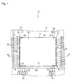
Fig. 1 is a plan view schematically illustrating a configuration for a portion where a semiconductor device is installed in a semiconductor package according to a first embodiment of the present invention; -
Fig. 2 is a cross-sectional view along a line II-II inFig. 1 ; -
Fig. 3 is a plan view schematically illustrating a configuration for a portion where a semiconductor device is installed in the semiconductor package prior to installation of the semiconductor device; -
Fig. 4 is a cross-sectional view schematically illustrating an enlarged view of a state in which a thickness of a positioning pattern is thinner than a height from a bottom surface of chipping on an outer periphery of the semiconductor device; -
Fig. 5 is a cross-sectional view schematically illustrating an enlarged view of a state where the outer periphery on which chipping has been formed abuts the positioning pattern; -
Fig. 6 is a cross-sectional view schematically illustrating an enlarged view of a state where the outer periphery on which chipping has been formed lifts onto the positioning pattern; -
Fig. 7 is a cross-sectional view schematically illustrating an enlarged view of a state in which the thickness of the positioning pattern is thicker than the height from the bottom surface of chipping on the outer periphery of the semiconductor device; -
Fig. 8 is a cross-sectional view schematically illustrating an enlarged view of a state in which the outer periphery on which chipping has been formed abuts the positioning pattern; -
Fig. 9 is a flowchart illustrating an overview of a method for manufacturing the semiconductor package; -
Fig. 10 is a plan view schematically illustrating an enlarged view of a state of abutment in the semiconductor device when an etching fillet is formed on an interior corner of an L-shaped positioning pattern; -
Fig. 11 is a plan view schematically illustrating an enlarged view of a state of abutment in the semiconductor device when a notch is formed on the interior corner of the L-shaped positioning pattern; -
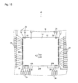
Fig. 12 is a plan view schematically illustrating a view of a configuration for a portion where a semiconductor device is installed in a semiconductor package according to a second embodiment of the present invention; -
Fig. 13 is a plan view schematically illustrating a view of a configuration for a portion where a semiconductor device is installed in the semiconductor package prior to installation of the semiconductor device; -
Fig. 14 is a cross-sectional view schematically illustrating a view of an example of behavior of an adhesive when the semiconductor device is installed on the substrate; and -
Fig. 15 is a plan view schematically illustrating a view of a configuration for a portion where a semiconductor device is installed in a semiconductor package according to a third embodiment of the present invention. - The particulars shown herein are by way of example and for purposes of illustrative discussion of the embodiments of the present invention only and are presented in the cause of providing what is believed to be the most useful and readily understood description of the principles and conceptual aspects of the present invention. In this regard, no attempt is made to show structural details of the present invention in more detail than is necessary for the fundamental understanding of the present invention, the description is taken with the drawings making apparent to those skilled in the art how the forms of the present invention may be embodied in practice.
- Hereafter, preferred embodiments of the present invention are described with reference to the drawings. As shown in
Figs. 1 and2 , asemiconductor package 10 according to a first embodiment of the present invention includes asemiconductor device 14 and asubstrate 16, thesemiconductor device 14 having straight line portions on anouter periphery 12 and thesubstrate 16 supporting thesemiconductor device 14. Afoil positioning pattern 18 that touches the straight line portions of thesemiconductor device 14 to regulate a position of thesemiconductor device 14 is formed on a front surface of thesubstrate 16. Other structures are not considered particularly essential to an understanding of the present embodiment, and thus descriptions thereof are omitted as appropriate. - The
semiconductor device 14 is a light receiving element that includes a photodiode array for detecting optical displacement. More specifically, thesemiconductor device 14 is rectangular and includes a firststraight line portion 20A and a secondstraight line portion 20B on theouter periphery 12, the firststraight line portion 20A and the secondstraight line portion 20B forming a right angle with respect to each other. Moreover, portions on theouter periphery 12 of thesemiconductor device 14 that are related to the firststraight line portion 20A and the secondstraight line portion 20B as an opposing side are also straight line portions. As shown inFig. 1 , when thesemiconductor device 14 is rectangular, a direction of the photodiode array (columnar direction of photodiodes) preferably matches a length direction of thesemiconductor device 14. Thesemiconductor device 14 has a thickness in a range of approximately 0.05 to 0.7 mm. The thickness is appropriately selected in consideration of a manufacturing process cost, yield ratio, and the like for the semiconductor device. Moreover, when thesemiconductor device 14 is clipped from a semiconductor wafer, irregularly shaped breakages called chipping may be formed on theouter periphery 12, such as damage or peeling of a surface layer film. For example, a portion on a bottom surface side of theouter periphery 12 may be missing. Such damage is preferably as small as possible. Processing requirements for the clipping process are considered such that a range where the damage occurs is less than 10 µm from a bottom surface. - A material for the
substrate 16 is a known material such as paper phenol, paper epoxy, glass composite, glass epoxy, Teflon (registered trademark), alumina, and LTCC. - A material for the
positioning pattern 18 is a foil such as copper foil and aluminum foil. As shown inFig. 3 , thepositioning pattern 18 has an "L" shape in a planar view. As shown inFig. 1 , thepositioning pattern 18 touches both the firststraight line portion 20A and the secondstraight line portion 20B. Thesemiconductor device 14 is rectangular. As shown inFig. 1 , when thepositioning pattern 18 has the "L" shape configured by two straight line portions of different lengths, the longer of the straight line portions of thepositioning pattern 18 preferably touches the longer of the straight line portions of the semiconductor device 14 (the secondstraight line portion 20B). In addition, anotch 22 having a shape indented away from a corner of thesemiconductor device 14 is formed on an interior corner of the L-shapedpositioning pattern 18. Moreover, the irregular breakage called chipping may form on theouter periphery 12 of thesemiconductor device 14 as described above. When a thickness A of thepositioning pattern 18 is thinner than a height K from the bottom surface of a missing portion on theouter periphery 12 of thesemiconductor device 14, as shown inFig. 4 , thesemiconductor device 14 abuts thepositioning pattern 18 at the missing portion on theouter periphery 12, as shown inFig. 5 . In addition, as shown inFig. 6 , thesemiconductor device 14 may also lift up on thepositioning pattern 18, which accordingly becomes a cause of reduction in positioning accuracy for thesemiconductor device 14. In contrast, when the thickness A of thepositioning pattern 18 is thicker than the height K from the bottom surface of the missing portion on theouter periphery 12 of thesemiconductor device 14, as shown inFig. 7 , thesemiconductor device 14 abuts thepositioning pattern 18 at a portion of theouter periphery 12 where no damage has occurred, as shown inFig. 8 , and thus thesemiconductor device 14 can be accurately positioned on thesubstrate 16. As described above, a clipping process for semiconductor devices has been considered such that a range where damage to theouter periphery 12 of thesemiconductor device 14 occurs is less than 10 µm from the bottom surface. Therefore, when the thickness of thepositioning pattern 18 is 10 µm or greater, an undamaged portion of theouter periphery 12 of thesemiconductor device 14 can reliably abut thepositioning pattern 18. Accordingly, the thickness of thepositioning pattern 18 is preferably 10 µm or greater. In addition, the thickness of thepositioning pattern 18 is preferably thinner than the thickness of thesemiconductor device 14. The thickness of thepositioning pattern 18 is typically 18 µm, 35 µm, 70 µm, and the like. - In addition, a
foil wiring pattern 24 is also formed on the front surface of thesubstrate 16. The material and thickness for thewiring pattern 24 are the same as those for thepositioning pattern 18. Thewiring pattern 24 is connected to terminals of thesemiconductor device 14 viabond wires 26. By making the thickness of thepositioning pattern 18 thinner than the thickness of thesemiconductor device 14, interference between thebond wires 26 and thepositioning pattern 18 can be avoided. - In addition, the
semiconductor package 10 is sealed by a sealingresin 28 on a side where thesemiconductor device 14 is installed on thesubstrate 16. A transparent epoxy-type resin, for example, may be used as a material for the sealingresin 28. - Next, following a flowchart in
Fig. 9 , a manufacturing method for thesemiconductor package 10 is described. First, thefoil positioning pattern 18 for regulating the position of thesemiconductor device 14 is formed on the front surface of the substrate 16 (S102: pattern forming process). In addition to thepositioning pattern 18, thewiring pattern 24 is also formed on the front surface of thesubstrate 16 in this process, thewiring pattern 24 having the same material and thickness as those of the positioning pattern 18 (seeFig. 3 ). Specifically, foil such as copper foil is spread across the front surface of thesubstrate 16 and is processed into the shapes of thepositioning pattern 18 and thewiring pattern 24 using a photolithography method. When a wiring pattern is also formed on a rear surface of thesubstrate 16, foil such as copper foil is also spread across the rear surface of thesubstrate 16 and is processed into the shape of the wiring pattern using the photolithography method. In addition, through-holes are formed in thesubstrate 16 so as to communicate with wirings on both surfaces. Furthermore, the through-holes are formed so as to be filled by plating in order to electrically connect the wiring patterns on both surfaces. - Next, the
semiconductor device 14 is installed on the front surface of thesubstrate 16 while regulating the position of thesemiconductor device 14 by abutting the firststraight line portion 20A and the secondstraight line portion 20B of thesemiconductor device 14 on the positioning pattern 18 (S104: semiconductor device installation process). When no notch is formed in the interior corner of the L-shapedpositioning pattern 18, as shown inFig. 10 , an etching fillet is formed in the interior corner of thepositioning pattern 18. There is thus a possibility that the corner of thesemiconductor device 14 and the interior corner of the L-shapedpositioning pattern 18 may interfere with each other and a gap may occur between thepositioning pattern 18 and the firststraight line portion 20A and/or the secondstraight line portion 20B of thesemiconductor device 14. However, in the present first embodiment, thenotch 22 is formed on the interior corner of the L-shapedpositioning pattern 18, thenotch 22 having a shape indented away from the corner of thesemiconductor device 14. Therefore, as shown inFig. 11 , the corner of thesemiconductor device 14 and the interior corner of the L-shapedpositioning pattern 18 do not interfere with each other. Accordingly, the firststraight line portion 20A and the secondstraight line portion 20B of thesemiconductor device 14 can reliably abut thepositioning pattern 18 and accurate positioning of thesemiconductor device 14 on thesubstrate 16 is possible. When thesemiconductor device 14 is installed on thesubstrate 16, an adhesive of an epoxy resin or the like is applied to a plurality of locations (for example, five locations) on the contact surfaces of thesubstrate 16 and/or thesemiconductor device 14. In addition, the terminals on thesemiconductor device 14 and thewiring pattern 24 are connected via thebond wires 26. - Next, the side where the
semiconductor device 14 has been installed on thesubstrate 16 is sealed by the sealing resin 28 (S106: resin sealing process). Specifically, thesemiconductor device 14 and thesubstrate 16 are installed in a mold of a resin molding apparatus such as a transfer molding apparatus. The side where thesemiconductor device 14 has been installed on thesubstrate 16 is then sealed by the sealingresin 28 so as to cover thesemiconductor device 14, thus completing thesemiconductor package 10. - As described above, in the pattern forming process (S102), the
foil positioning pattern 18 can be formed with a high degree of accuracy on the front surface of thesubstrate 16 along with thefoil wiring pattern 24 using a method such as lithography. In addition, by abutting the firststraight line portion 20A and the secondstraight line portion 20B of thesemiconductor device 14 on thepositioning pattern 18, thesemiconductor device 14 can be positioned and installed on the front surface of thesubstrate 16 with a high degree of accuracy. Accordingly, with thesemiconductor package 10, highly accurate positioning of thesemiconductor device 14 can be achieved at a low cost. - In the present first embodiment, the
notch 22 having a shape indented away from the corner of thesemiconductor device 14 is formed on the interior corner of the L-shapedpositioning pattern 18. However, in a case where the corner of thesemiconductor device 14 has a chamfered shape and the corner of thesemiconductor device 14 and the interior corner of the L-shapedpositioning pattern 18 do not interfere with each other even when the etching fillet is formed on the interior corner of the L-shapedpositioning pattern 18, for example, no notch need be formed on the interior corner of the L-shapedpositioning pattern 18. - Next, a second embodiment of the present invention is described. A single (one) L-shaped
positioning pattern 18 is formed on the front surface of thesubstrate 16 in thesemiconductor package 10 of the first embodiment. In contrast, as shown inFigs. 12 and13 , asemiconductor package 30 in the present second embodiment includes apositioning pattern 32 formed on the front surface of thesubstrate 16, thepositioning pattern 32 being divided into threepositioning pattern elements Figs. 1 to 11 and descriptions thereof are omitted. - The
positioning pattern 32 touches the firststraight line portion 20A at thepositioning pattern element 32A and touches the secondstraight line portion 20B at thepositioning pattern elements positioning pattern elements positioning pattern element 32A touches the firststraight line portion 20A at a portion away from an end portion of the firststraight line portion 20A. Meanwhile, thepositioning pattern elements straight line portion 20B. In addition, thepositioning pattern elements straight line portion 20B. A portion of thepositioning pattern elements straight line portion 20B past the respective end portions of the secondstraight line portion 20B. The projecting portions do not touch the secondstraight line portion 20B. The material and thickness for thepositioning pattern 32 are the same as those for thepositioning pattern 18 and thewiring pattern 24. When thesemiconductor device 14 is rectangular, thepositioning pattern 32 preferably touches two points on the longer of the straight line portions of the semiconductor device 14 (the secondstraight line portion 20B), the two points having a span that is as long as possible. As shown inFig. 12 , thepositioning pattern 32 more preferably touches both end portions of the longer of the straight line portions of the semiconductor device 14 (the secondstraight line portion 20B). - The
positioning pattern 32 of thesemiconductor package 30 in the present second embodiment is also foil. Therefore, in the pattern forming process (S102), thepositioning pattern 32 can be formed with a high degree of accuracy on the front surface of thesubstrate 16 along with thewiring pattern 24 using a method such as lithography. In addition, in the semiconductor device installation process (S104), the firststraight line portion 20A of thesemiconductor device 14 abuts thepositioning pattern element 32A, and the secondstraight line portion 20B abuts thepositioning pattern elements semiconductor device 14 can be positioned and installed on the front surface of thesubstrate 16 with a high degree of accuracy. Accordingly, highly accurate positioning of thesemiconductor device 14 can be achieved at a low cost in thesemiconductor package 30, as well. - In addition, as shown in
Fig. 14 , when a large amount of an adhesive 34 is applied to the contact surfaces of thesemiconductor device 14 and thesubstrate 16 and the adhesive 34 sticks out from the contact surfaces, there is a possibility that the excess adhesive 34 may spill over onto thesemiconductor device 14 from between the firststraight line portion 20A and the secondstraight line portion 20B of thesemiconductor device 14 and thepositioning pattern 32 and bond to the terminals of thesemiconductor device 14. However, thepositioning pattern elements straight line portion 20B and, in addition, thepositioning pattern elements positioning pattern elements positioning pattern elements semiconductor device 14 and bonds to the terminals of thesemiconductor device 14 is unlikely to occur. - The portion of the L-shaped
positioning pattern 18 touching the firststraight line portion 20A and/or the portion touching the secondstraight line portion 20B may be separated (in the extension direction of the touching straight line portion) in the first embodiment, as well. Thereby, a situation in which the excess adhesive 34 spills over onto thesemiconductor device 14 and bonds to the terminals of thesemiconductor device 14 is unlikely to occur, similar to the present second embodiment. - Next, a third embodiment of the present invention is described. In the
semiconductor package 10 of the first embodiment and thesemiconductor package 30 of the second embodiment, thepositioning patterns straight line portion 20A and the secondstraight line portion 20B of thesemiconductor device 14. In contrast, as shown inFig. 15 , in asemiconductor package 40 in the present third embodiment, apositioning pattern 42 touches only the secondstraight line portion 20B of thesemiconductor device 14 and does not touch the firststraight line portion 20A. In addition, positions of the end portions of the secondstraight line portion 20B and positions of end portions of thepositioning pattern 42 are matched up. Other structures are similar to the first and second embodiments. Therefore, similar structures are given the same reference numerals as those inFigs. 1 to 14 and descriptions thereof are omitted. - The
positioning pattern 42 is configured withpositioning pattern elements straight line portion 20B. More specifically, thepositioning pattern elements straight line portion 20B. The position of the end portion of thepositioning pattern element 42A matches up (i.e., aligns) with the position of a first end portion of the secondstraight line portion 20B. The position of the end portion of thepositioning pattern element 42B matches up (i.e., aligns) with the position of a second end portion of the secondstraight line portion 20B. The material and thickness for thepositioning pattern 42 are the same as those for thepositioning pattern 18, thepositioning pattern 32, and thewiring pattern 24. When thesemiconductor device 14 is rectangular, as shown inFig. 15 , thepositioning pattern 42 preferably touches the longer of the straight line portions of the semiconductor device 14 (the secondstraight line portion 20B). In addition, as shown inFig. 15 , thepositioning pattern 42 more preferably touches both ends of the longer of the straight line portions of the semiconductor device 14 (the secondstraight line portion 20B). - The
positioning pattern 42 of thesemiconductor package 40 in the present third embodiment is also foil. Therefore, in the pattern forming process (S102), thepositioning pattern 42 can be formed with a high degree of accuracy on the front surface of thesubstrate 16 along with thewiring pattern 24 using a method such as lithography. Moreover, in the semiconductor device installation process (S104), the secondstraight line portion 20B of thesemiconductor device 14 abuts thepositioning pattern elements straight line portion 20B is matched up with the position of the end portion of one of thepositioning pattern elements semiconductor device 14 can be positioned and installed on the front surface of thesubstrate 16 with a high degree of accuracy. When the position of the first end portion of the secondstraight line portion 20B is matched up with the position of the end portion of one of thepositioning pattern elements straight line portion 20B automatically matches up with the position of the end portion of the second positioning pattern element. Accordingly, highly accurate positioning of thesemiconductor device 14 can be achieved at a low cost in thesemiconductor package 40, as well. In addition, thepositioning pattern 42 does not touch the firststraight line portion 20A of thesemiconductor device 14. Therefore, theexcess adhesive 34 does not spiller over onto thesemiconductor device 14 from between the firststraight line portion 20A and the positioning pattern to bond to the terminals of thesemiconductor device 14. In addition, thepositioning pattern elements straight line portion 20B. Therefore, a situation in which the excess adhesive 34 spills over onto thesemiconductor device 14 from between the secondstraight line portion 20B and thepositioning pattern 42 to bond to the terminals of thesemiconductor device 14 is unlikely to occur. - In the present third embodiment, the position of the end portion of the
positioning pattern element 42A matches up with the position of the first end portion of the secondstraight line portion 20B and the position of the end portion of thepositioning pattern element 42B matches up with the position of the second end portion of the secondstraight line portion 20B. However, when the position of the end portion of either one of the two positioning pattern elements is matched up with the position of one end portion of the secondstraight line portion 20B, thesemiconductor device 14 can be accurately positioned on thesubstrate 16. Therefore, the position of the end portion of the other of the two positioning pattern elements does not need to match up with the position of the end portion of the secondstraight line portion 20B. For example, the end portion of the other positioning pattern element may project further than the position of the end portion of the secondstraight line portion 20B. - In addition, in the present third embodiment, the
positioning pattern elements straight line portion 20B. However, when the situation of the excess adhesive does not occur, the positioning pattern does not need to be separated in the extension direction of the secondstraight line portion 20B. - In addition, the
positioning pattern elements straight line portion 20B in the second embodiment, as well. However, when the situation of the excess adhesive does not occur, the portion of the positioning pattern touching the secondstraight line portion 20B does not need to be separated in the extension direction of the secondstraight line portion 20B. For example, the positioning pattern may be configured with one positioning pattern element touching the firststraight line portion 20A and one positioning pattern element touching the secondstraight line portion 20B. - In addition, in the first through third embodiments, the
wiring pattern 24 may be formed on the front surface of thesubstrate 16 along with thepositioning patterns wiring pattern 24 may also be separate from the process of forming thepositioning patterns positioning patterns - In addition, in the first through third embodiments, the
semiconductor device 14 is rectangular. However, the present invention may be applied to a semiconductor package that includes a semiconductor device having a shape other than rectangular as long as the shape has a straight line portion on the outer periphery. - In addition, in the first through third embodiments, the
semiconductor device 14 is the light receiving element that includes the photodiode array for detecting optical displacement. However, the present invention may be applied to a semiconductor package that includes a different optical semiconductor device or a semiconductor device other than an optical semiconductor device. When the semiconductor package includes the semiconductor device other than the optical semiconductor device, the sealing resin may, for example, be a non-transparent resin such as a black resin. - The present invention may be used in a semiconductor package that includes a semiconductor device and a substrate supporting the semiconductor device.
- It is noted that the foregoing examples have been provided merely for the purpose of explanation and are in no way to be construed as limiting of the present invention. While the present invention has been described with reference to exemplary embodiments, it is understood that the words which have been used herein are words of description and illustration, rather than words of limitation. Changes may be made, within the purview of the appended claims, as presently stated and as amended, without departing from the scope and spirit of the present invention in its aspects. Although the present invention has been described herein with reference to particular structures, materials and embodiments, the present invention is not intended to be limited to the particulars disclosed herein; rather, the present invention extends to all functionally equivalent structures, methods and uses, such as are within the scope of the appended claims.
- The present invention is not limited to the above described embodiments, and various variations and modifications may be possible without departing from the scope of the present invention.
Claims (9)
- A semiconductor package comprising:a semiconductor having a straight line segment on an outer periphery;a substrate supporting the semiconductor; anda foil positioning pattern located on a front surface of the substrate, the positioning pattern touching the straight line segment of the semiconductor to set a position of the semiconductor.
- The semiconductor package according to claim 1, wherein:the semiconductor includes, as the straight line segment on the outer periphery, a first straight line segment and a second straight line segment forming a right angle with respect to each other; andthe positioning pattern touches both the first straight line segment and the second straight line segment.
- The semiconductor package according to claim 2, wherein the positioning pattern has an "L" shape.
- The semiconductor package according to claim 1, wherein
the positioning pattern touches only one of the straight line segments on the outer periphery of the semiconductor; and
a position of an end of the positioning pattern aligns with a position of an end of the straight line segment the positioning pattern touches. - The semiconductor package according to any one of the preceding claims, further comprising a notch having a shape indented away from a corner of the semiconductor located on an interior corner of the positioning pattern.
- The semiconductor package according to any one of the preceding claims, wherein the positioning pattern is divided into a plurality of positioning pattern elements.
- The semiconductor package according to any one of the preceding claims, further comprising a foil wiring pattern located on the front surface of the substrate, a material and thickness for the wiring pattern being the same as those for the positioning pattern.
- A method for manufacturing a semiconductor package comprising:pattern forming to form a foil-positioning pattern for regulating a position of a semiconductor device on a front surface of a substrate supporting the semiconductor device, the semiconductor device having a straight line portion on an outer periphery; andinstalling the semiconductor device on the front surface of the substrate while regulating the position of the semiconductor device by abutting the straight line portion of the semiconductor device on the positioning pattern.
- The method for manufacturing the semiconductor package according to claim 8, wherein a wiring pattern is formed in said pattern forming on the front surface of the substrate along with the positioning pattern, a material and thickness for the wiring pattern being the same as those for the positioning pattern.
Applications Claiming Priority (1)
| Application Number | Priority Date | Filing Date | Title |
|---|---|---|---|
| JP2012006442A JP5896752B2 (en) | 2012-01-16 | 2012-01-16 | Semiconductor package and manufacturing method thereof |
Publications (3)
| Publication Number | Publication Date |
|---|---|
| EP2615637A2 true EP2615637A2 (en) | 2013-07-17 |
| EP2615637A3 EP2615637A3 (en) | 2017-04-19 |
| EP2615637B1 EP2615637B1 (en) | 2018-08-22 |
Family
ID=47740735
Family Applications (1)
| Application Number | Title | Priority Date | Filing Date |
|---|---|---|---|
| EP13000145.6A Active EP2615637B1 (en) | 2012-01-16 | 2013-01-11 | Semiconductor package and method for manufacturing the same |
Country Status (4)
| Country | Link |
|---|---|
| US (1) | US8987905B2 (en) |
| EP (1) | EP2615637B1 (en) |
| JP (1) | JP5896752B2 (en) |
| CN (1) | CN103208484B (en) |
Families Citing this family (3)
| Publication number | Priority date | Publication date | Assignee | Title |
|---|---|---|---|---|
| CN105190855B (en) * | 2013-03-13 | 2017-09-19 | 丰田自动车株式会社 | Semiconductor device |
| JP6177427B2 (en) * | 2014-04-04 | 2017-08-09 | 三菱電機株式会社 | Printed wiring board unit |
| EP4273920A1 (en) * | 2022-05-04 | 2023-11-08 | Murata Manufacturing Co., Ltd. | Electronic component with aligned die |
Family Cites Families (15)
| Publication number | Priority date | Publication date | Assignee | Title |
|---|---|---|---|---|
| EP0214692B1 (en) | 1985-09-05 | 1991-12-04 | Koninklijke Philips Electronics N.V. | Monitoring a conflict detector for traffic-lights |
| JP2871696B2 (en) | 1988-06-30 | 1999-03-17 | 日本電気株式会社 | Integrated circuit device |
| JPH09189515A (en) | 1996-01-12 | 1997-07-22 | Mitsutoyo Corp | Optical displacement detection device |
| JPH09236454A (en) | 1996-03-01 | 1997-09-09 | Yaskawa Electric Corp | Optical encoder and light receiving element positioning method thereof |
| JP3292723B2 (en) | 2000-05-26 | 2002-06-17 | アルス電子株式会社 | Semiconductor package and manufacturing method thereof |
| JP2002333309A (en) | 2001-05-09 | 2002-11-22 | Disco Abrasive Syst Ltd | Chipping measuring device and method |
| JP2002353578A (en) * | 2001-05-22 | 2002-12-06 | Murata Mfg Co Ltd | Substrate for surface mount component and method of mounting surface mount component on substrate |
| JP4775750B2 (en) | 2001-07-31 | 2011-09-21 | 株式会社安川電機 | Optical encoder and optical encoder manufacturing method |
| JP3745279B2 (en) * | 2002-01-16 | 2006-02-15 | 日本航空電子工業株式会社 | DVI optical extension cable connection and external power input confirmation system |
| JP2004363171A (en) * | 2003-06-02 | 2004-12-24 | Seiko Epson Corp | Wiring board and its manufacturing method, chip module, electro-optical device and its manufacturing method, and electronic equipment |
| JP2005236039A (en) * | 2004-02-19 | 2005-09-02 | Tdk Corp | Semiconductor IC-embedded substrate, manufacturing method thereof, and semiconductor IC-embedded module |
| US8009439B2 (en) * | 2007-11-30 | 2011-08-30 | Raytheon Company | Metal foil interconnection of electrical devices |
| JP4544301B2 (en) * | 2007-12-26 | 2010-09-15 | ソニー株式会社 | Image display device and connector display method |
| JP5417151B2 (en) * | 2009-12-18 | 2014-02-12 | 株式会社東芝 | Optical wiring cable and optical power control method |
| CN102142405B (en) * | 2010-10-27 | 2015-04-15 | 日月光半导体制造股份有限公司 | Semiconductor package structure and manufacturing method thereof |
-
2012
- 2012-01-16 JP JP2012006442A patent/JP5896752B2/en active Active
- 2012-12-12 US US13/712,092 patent/US8987905B2/en active Active
-
2013
- 2013-01-11 EP EP13000145.6A patent/EP2615637B1/en active Active
- 2013-01-15 CN CN201310013792.1A patent/CN103208484B/en active Active
Also Published As
| Publication number | Publication date |
|---|---|
| EP2615637B1 (en) | 2018-08-22 |
| JP2013145849A (en) | 2013-07-25 |
| JP5896752B2 (en) | 2016-03-30 |
| CN103208484B (en) | 2017-11-24 |
| US8987905B2 (en) | 2015-03-24 |
| CN103208484A (en) | 2013-07-17 |
| US20130181353A1 (en) | 2013-07-18 |
| EP2615637A3 (en) | 2017-04-19 |
Similar Documents
| Publication | Publication Date | Title |
|---|---|---|
| US8860153B2 (en) | Semiconductor packages, systems, and methods of formation thereof | |
| CN1276702C (en) | Method for positioning on base and placing view-point characteristic of semiconductor piece | |
| US20070034402A1 (en) | Tape substrate, tape package and flat panel display using same | |
| CN1318206A (en) | Method of dicing chip from semiconductor wafer and structure of groove provided in dicing area | |
| EP2615637B1 (en) | Semiconductor package and method for manufacturing the same | |
| US20140217581A1 (en) | Electronic component, mother substrate, and electronic component manufacturing method | |
| US7833829B2 (en) | MEMS devices and methods of assembling micro electromechanical systems (MEMS) | |
| KR101952847B1 (en) | System of measuring warpage and mentod of measuring warpage | |
| CN112185823B (en) | Handling one or more carrier bodies and electronic devices by multiple alignment | |
| KR102446236B1 (en) | Substrate bonding apparatus | |
| US10454240B2 (en) | Method of producing an optoelectronic component | |
| US10366813B2 (en) | High-precision additive formation of electrical resistors | |
| US7518157B2 (en) | Optoelectronic component assembly | |
| US20190339478A1 (en) | Optical device | |
| US11282880B2 (en) | Linear image sensor and method for manufacturing same | |
| CN1116697C (en) | Method for producing film carrier, mask and film carrier used in the method | |
| US20240387436A1 (en) | Hermetic package device, and device module | |
| US20230360945A1 (en) | Electronic component with aligned die | |
| US9173286B2 (en) | Flexible-rigid circuit board composite and method for producing a flexible-rigid circuit board composite | |
| CN101055863A (en) | Circuit board and circuit structure | |
| KR101681632B1 (en) | Method for bonding flat materials | |
| US11462667B2 (en) | Electronic component, method of manufacturing electronic component, and electronic device | |
| JP2012084646A (en) | Tab tape and method for manufacturing the same | |
| CN118693167A (en) | Optical device | |
| CN110324968A (en) | Circuit substrate and its manufacturing method |
Legal Events
| Date | Code | Title | Description |
|---|---|---|---|
| PUAI | Public reference made under article 153(3) epc to a published international application that has entered the european phase |
Free format text: ORIGINAL CODE: 0009012 |
|
| AK | Designated contracting states |
Kind code of ref document: A2 Designated state(s): AL AT BE BG CH CY CZ DE DK EE ES FI FR GB GR HR HU IE IS IT LI LT LU LV MC MK MT NL NO PL PT RO RS SE SI SK SM TR |
|
| AX | Request for extension of the european patent |
Extension state: BA ME |
|
| PUAL | Search report despatched |
Free format text: ORIGINAL CODE: 0009013 |
|
| RIC1 | Information provided on ipc code assigned before grant |
Ipc: H01L 23/544 20060101ALI20170307BHEP Ipc: H01L 21/60 20060101ALI20170307BHEP Ipc: H01L 23/498 20060101AFI20170307BHEP |
|
| AK | Designated contracting states |
Kind code of ref document: A3 Designated state(s): AL AT BE BG CH CY CZ DE DK EE ES FI FR GB GR HR HU IE IS IT LI LT LU LV MC MK MT NL NO PL PT RO RS SE SI SK SM TR |
|
| AX | Request for extension of the european patent |
Extension state: BA ME |
|
| STAA | Information on the status of an ep patent application or granted ep patent |
Free format text: STATUS: REQUEST FOR EXAMINATION WAS MADE |
|
| 17P | Request for examination filed |
Effective date: 20170914 |
|
| RBV | Designated contracting states (corrected) |
Designated state(s): AL AT BE BG CH CY CZ DE DK EE ES FI FR GB GR HR HU IE IS IT LI LT LU LV MC MK MT NL NO PL PT RO RS SE SI SK SM TR |
|
| RIN1 | Information on inventor provided before grant (corrected) |
Inventor name: MIZUNO, KEN Inventor name: YAKU, TORU |
|
| GRAP | Despatch of communication of intention to grant a patent |
Free format text: ORIGINAL CODE: EPIDOSNIGR1 |
|
| STAA | Information on the status of an ep patent application or granted ep patent |
Free format text: STATUS: GRANT OF PATENT IS INTENDED |
|
| RIC1 | Information provided on ipc code assigned before grant |
Ipc: H01L 23/544 20060101ALI20180427BHEP Ipc: H01L 23/498 20060101AFI20180427BHEP Ipc: H01L 21/60 20060101ALI20180427BHEP |
|
| INTG | Intention to grant announced |
Effective date: 20180524 |
|
| RAP1 | Party data changed (applicant data changed or rights of an application transferred) |
Owner name: MITUTOYO CORPORATION |
|
| GRAS | Grant fee paid |
Free format text: ORIGINAL CODE: EPIDOSNIGR3 |
|
| GRAA | (expected) grant |
Free format text: ORIGINAL CODE: 0009210 |
|
| STAA | Information on the status of an ep patent application or granted ep patent |
Free format text: STATUS: THE PATENT HAS BEEN GRANTED |
|
| AK | Designated contracting states |
Kind code of ref document: B1 Designated state(s): AL AT BE BG CH CY CZ DE DK EE ES FI FR GB GR HR HU IE IS IT LI LT LU LV MC MK MT NL NO PL PT RO RS SE SI SK SM TR |
|
| REG | Reference to a national code |
Ref country code: GB Ref legal event code: FG4D |
|
| REG | Reference to a national code |
Ref country code: CH Ref legal event code: EP |
|
| REG | Reference to a national code |
Ref country code: AT Ref legal event code: REF Ref document number: 1033435 Country of ref document: AT Kind code of ref document: T Effective date: 20180915 |
|
| REG | Reference to a national code |
Ref country code: IE Ref legal event code: FG4D |
|
| REG | Reference to a national code |
Ref country code: DE Ref legal event code: R096 Ref document number: 602013042248 Country of ref document: DE |
|
| REG | Reference to a national code |
Ref country code: NL Ref legal event code: MP Effective date: 20180822 |
|
| REG | Reference to a national code |
Ref country code: LT Ref legal event code: MG4D |
|
| PG25 | Lapsed in a contracting state [announced via postgrant information from national office to epo] |
Ref country code: NO Free format text: LAPSE BECAUSE OF FAILURE TO SUBMIT A TRANSLATION OF THE DESCRIPTION OR TO PAY THE FEE WITHIN THE PRESCRIBED TIME-LIMIT Effective date: 20181122 Ref country code: BG Free format text: LAPSE BECAUSE OF FAILURE TO SUBMIT A TRANSLATION OF THE DESCRIPTION OR TO PAY THE FEE WITHIN THE PRESCRIBED TIME-LIMIT Effective date: 20181122 Ref country code: GR Free format text: LAPSE BECAUSE OF FAILURE TO SUBMIT A TRANSLATION OF THE DESCRIPTION OR TO PAY THE FEE WITHIN THE PRESCRIBED TIME-LIMIT Effective date: 20181123 Ref country code: RS Free format text: LAPSE BECAUSE OF FAILURE TO SUBMIT A TRANSLATION OF THE DESCRIPTION OR TO PAY THE FEE WITHIN THE PRESCRIBED TIME-LIMIT Effective date: 20180822 Ref country code: SE Free format text: LAPSE BECAUSE OF FAILURE TO SUBMIT A TRANSLATION OF THE DESCRIPTION OR TO PAY THE FEE WITHIN THE PRESCRIBED TIME-LIMIT Effective date: 20180822 Ref country code: FI Free format text: LAPSE BECAUSE OF FAILURE TO SUBMIT A TRANSLATION OF THE DESCRIPTION OR TO PAY THE FEE WITHIN THE PRESCRIBED TIME-LIMIT Effective date: 20180822 Ref country code: LT Free format text: LAPSE BECAUSE OF FAILURE TO SUBMIT A TRANSLATION OF THE DESCRIPTION OR TO PAY THE FEE WITHIN THE PRESCRIBED TIME-LIMIT Effective date: 20180822 Ref country code: NL Free format text: LAPSE BECAUSE OF FAILURE TO SUBMIT A TRANSLATION OF THE DESCRIPTION OR TO PAY THE FEE WITHIN THE PRESCRIBED TIME-LIMIT Effective date: 20180822 Ref country code: IS Free format text: LAPSE BECAUSE OF FAILURE TO SUBMIT A TRANSLATION OF THE DESCRIPTION OR TO PAY THE FEE WITHIN THE PRESCRIBED TIME-LIMIT Effective date: 20181222 |
|
| REG | Reference to a national code |
Ref country code: AT Ref legal event code: MK05 Ref document number: 1033435 Country of ref document: AT Kind code of ref document: T Effective date: 20180822 |
|
| PG25 | Lapsed in a contracting state [announced via postgrant information from national office to epo] |
Ref country code: LV Free format text: LAPSE BECAUSE OF FAILURE TO SUBMIT A TRANSLATION OF THE DESCRIPTION OR TO PAY THE FEE WITHIN THE PRESCRIBED TIME-LIMIT Effective date: 20180822 Ref country code: AL Free format text: LAPSE BECAUSE OF FAILURE TO SUBMIT A TRANSLATION OF THE DESCRIPTION OR TO PAY THE FEE WITHIN THE PRESCRIBED TIME-LIMIT Effective date: 20180822 Ref country code: HR Free format text: LAPSE BECAUSE OF FAILURE TO SUBMIT A TRANSLATION OF THE DESCRIPTION OR TO PAY THE FEE WITHIN THE PRESCRIBED TIME-LIMIT Effective date: 20180822 |
|
| PG25 | Lapsed in a contracting state [announced via postgrant information from national office to epo] |
Ref country code: EE Free format text: LAPSE BECAUSE OF FAILURE TO SUBMIT A TRANSLATION OF THE DESCRIPTION OR TO PAY THE FEE WITHIN THE PRESCRIBED TIME-LIMIT Effective date: 20180822 Ref country code: PL Free format text: LAPSE BECAUSE OF FAILURE TO SUBMIT A TRANSLATION OF THE DESCRIPTION OR TO PAY THE FEE WITHIN THE PRESCRIBED TIME-LIMIT Effective date: 20180822 Ref country code: AT Free format text: LAPSE BECAUSE OF FAILURE TO SUBMIT A TRANSLATION OF THE DESCRIPTION OR TO PAY THE FEE WITHIN THE PRESCRIBED TIME-LIMIT Effective date: 20180822 Ref country code: RO Free format text: LAPSE BECAUSE OF FAILURE TO SUBMIT A TRANSLATION OF THE DESCRIPTION OR TO PAY THE FEE WITHIN THE PRESCRIBED TIME-LIMIT Effective date: 20180822 Ref country code: IT Free format text: LAPSE BECAUSE OF FAILURE TO SUBMIT A TRANSLATION OF THE DESCRIPTION OR TO PAY THE FEE WITHIN THE PRESCRIBED TIME-LIMIT Effective date: 20180822 Ref country code: CZ Free format text: LAPSE BECAUSE OF FAILURE TO SUBMIT A TRANSLATION OF THE DESCRIPTION OR TO PAY THE FEE WITHIN THE PRESCRIBED TIME-LIMIT Effective date: 20180822 Ref country code: ES Free format text: LAPSE BECAUSE OF FAILURE TO SUBMIT A TRANSLATION OF THE DESCRIPTION OR TO PAY THE FEE WITHIN THE PRESCRIBED TIME-LIMIT Effective date: 20180822 |
|
| REG | Reference to a national code |
Ref country code: DE Ref legal event code: R097 Ref document number: 602013042248 Country of ref document: DE |
|
| PG25 | Lapsed in a contracting state [announced via postgrant information from national office to epo] |
Ref country code: SK Free format text: LAPSE BECAUSE OF FAILURE TO SUBMIT A TRANSLATION OF THE DESCRIPTION OR TO PAY THE FEE WITHIN THE PRESCRIBED TIME-LIMIT Effective date: 20180822 Ref country code: DK Free format text: LAPSE BECAUSE OF FAILURE TO SUBMIT A TRANSLATION OF THE DESCRIPTION OR TO PAY THE FEE WITHIN THE PRESCRIBED TIME-LIMIT Effective date: 20180822 Ref country code: SM Free format text: LAPSE BECAUSE OF FAILURE TO SUBMIT A TRANSLATION OF THE DESCRIPTION OR TO PAY THE FEE WITHIN THE PRESCRIBED TIME-LIMIT Effective date: 20180822 |
|
| PLBE | No opposition filed within time limit |
Free format text: ORIGINAL CODE: 0009261 |
|
| STAA | Information on the status of an ep patent application or granted ep patent |
Free format text: STATUS: NO OPPOSITION FILED WITHIN TIME LIMIT |
|
| 26N | No opposition filed |
Effective date: 20190523 |
|
| PG25 | Lapsed in a contracting state [announced via postgrant information from national office to epo] |
Ref country code: MC Free format text: LAPSE BECAUSE OF FAILURE TO SUBMIT A TRANSLATION OF THE DESCRIPTION OR TO PAY THE FEE WITHIN THE PRESCRIBED TIME-LIMIT Effective date: 20180822 Ref country code: SI Free format text: LAPSE BECAUSE OF FAILURE TO SUBMIT A TRANSLATION OF THE DESCRIPTION OR TO PAY THE FEE WITHIN THE PRESCRIBED TIME-LIMIT Effective date: 20180822 |
|
| REG | Reference to a national code |
Ref country code: CH Ref legal event code: PL |
|
| GBPC | Gb: european patent ceased through non-payment of renewal fee |
Effective date: 20190111 |
|
| PG25 | Lapsed in a contracting state [announced via postgrant information from national office to epo] |
Ref country code: LU Free format text: LAPSE BECAUSE OF NON-PAYMENT OF DUE FEES Effective date: 20190111 |
|
| REG | Reference to a national code |
Ref country code: BE Ref legal event code: MM Effective date: 20190131 |
|
| REG | Reference to a national code |
Ref country code: IE Ref legal event code: MM4A |
|
| PG25 | Lapsed in a contracting state [announced via postgrant information from national office to epo] |
Ref country code: FR Free format text: LAPSE BECAUSE OF NON-PAYMENT OF DUE FEES Effective date: 20190131 |
|
| PG25 | Lapsed in a contracting state [announced via postgrant information from national office to epo] |
Ref country code: BE Free format text: LAPSE BECAUSE OF NON-PAYMENT OF DUE FEES Effective date: 20190131 |
|
| PG25 | Lapsed in a contracting state [announced via postgrant information from national office to epo] |
Ref country code: CH Free format text: LAPSE BECAUSE OF NON-PAYMENT OF DUE FEES Effective date: 20190131 Ref country code: GB Free format text: LAPSE BECAUSE OF NON-PAYMENT OF DUE FEES Effective date: 20190111 Ref country code: LI Free format text: LAPSE BECAUSE OF NON-PAYMENT OF DUE FEES Effective date: 20190131 |
|
| PG25 | Lapsed in a contracting state [announced via postgrant information from national office to epo] |
Ref country code: IE Free format text: LAPSE BECAUSE OF NON-PAYMENT OF DUE FEES Effective date: 20190111 |
|
| PG25 | Lapsed in a contracting state [announced via postgrant information from national office to epo] |
Ref country code: TR Free format text: LAPSE BECAUSE OF FAILURE TO SUBMIT A TRANSLATION OF THE DESCRIPTION OR TO PAY THE FEE WITHIN THE PRESCRIBED TIME-LIMIT Effective date: 20180822 |
|
| PG25 | Lapsed in a contracting state [announced via postgrant information from national office to epo] |
Ref country code: PT Free format text: LAPSE BECAUSE OF FAILURE TO SUBMIT A TRANSLATION OF THE DESCRIPTION OR TO PAY THE FEE WITHIN THE PRESCRIBED TIME-LIMIT Effective date: 20181222 Ref country code: MT Free format text: LAPSE BECAUSE OF NON-PAYMENT OF DUE FEES Effective date: 20190111 |
|
| PG25 | Lapsed in a contracting state [announced via postgrant information from national office to epo] |
Ref country code: CY Free format text: LAPSE BECAUSE OF FAILURE TO SUBMIT A TRANSLATION OF THE DESCRIPTION OR TO PAY THE FEE WITHIN THE PRESCRIBED TIME-LIMIT Effective date: 20180822 |
|
| PG25 | Lapsed in a contracting state [announced via postgrant information from national office to epo] |
Ref country code: HU Free format text: LAPSE BECAUSE OF FAILURE TO SUBMIT A TRANSLATION OF THE DESCRIPTION OR TO PAY THE FEE WITHIN THE PRESCRIBED TIME-LIMIT; INVALID AB INITIO Effective date: 20130111 |
|
| PG25 | Lapsed in a contracting state [announced via postgrant information from national office to epo] |
Ref country code: MK Free format text: LAPSE BECAUSE OF FAILURE TO SUBMIT A TRANSLATION OF THE DESCRIPTION OR TO PAY THE FEE WITHIN THE PRESCRIBED TIME-LIMIT Effective date: 20180822 |
|
| REG | Reference to a national code |
Ref country code: DE Ref legal event code: R079 Ref document number: 602013042248 Country of ref document: DE Free format text: PREVIOUS MAIN CLASS: H01L0023498000 Ipc: H10W0070620000 |
|
| PGFP | Annual fee paid to national office [announced via postgrant information from national office to epo] |
Ref country code: DE Payment date: 20260121 Year of fee payment: 14 |