EP2614554B1 - Hochleistungs-lcl-kombinator - Google Patents
Hochleistungs-lcl-kombinator Download PDFInfo
- Publication number
- EP2614554B1 EP2614554B1 EP11823999.5A EP11823999A EP2614554B1 EP 2614554 B1 EP2614554 B1 EP 2614554B1 EP 11823999 A EP11823999 A EP 11823999A EP 2614554 B1 EP2614554 B1 EP 2614554B1
- Authority
- EP
- European Patent Office
- Prior art keywords
- combiner
- radio frequency
- coaxial cables
- output
- capacitance
- Prior art date
- Legal status (The legal status is an assumption and is not a legal conclusion. Google has not performed a legal analysis and makes no representation as to the accuracy of the status listed.)
- Not-in-force
Links
Images

Classifications
-
- H—ELECTRICITY
- H01—ELECTRIC ELEMENTS
- H01P—WAVEGUIDES; RESONATORS, LINES, OR OTHER DEVICES OF THE WAVEGUIDE TYPE
- H01P5/00—Coupling devices of the waveguide type
- H01P5/12—Coupling devices having more than two ports
- H01P5/16—Conjugate devices, i.e. devices having at least one port decoupled from one other port
- H01P5/18—Conjugate devices, i.e. devices having at least one port decoupled from one other port consisting of two coupled guides, e.g. directional couplers
- H01P5/183—Conjugate devices, i.e. devices having at least one port decoupled from one other port consisting of two coupled guides, e.g. directional couplers at least one of the guides being a coaxial line
-
- G—PHYSICS
- G06—COMPUTING OR CALCULATING; COUNTING
- G06G—ANALOGUE COMPUTERS
- G06G7/00—Devices in which the computing operation is performed by varying electric or magnetic quantities
- G06G7/12—Arrangements for performing computing operations, e.g. operational amplifiers specially adapted therefor
-
- H—ELECTRICITY
- H03—ELECTRONIC CIRCUITRY
- H03F—AMPLIFIERS
- H03F3/00—Amplifiers with only discharge tubes or only semiconductor devices as amplifying elements
- H03F3/189—High-frequency amplifiers, e.g. radio frequency amplifiers
-
- H—ELECTRICITY
- H03—ELECTRONIC CIRCUITRY
- H03F—AMPLIFIERS
- H03F3/00—Amplifiers with only discharge tubes or only semiconductor devices as amplifying elements
- H03F3/189—High-frequency amplifiers, e.g. radio frequency amplifiers
- H03F3/19—High-frequency amplifiers, e.g. radio frequency amplifiers with semiconductor devices only
- H03F3/195—High-frequency amplifiers, e.g. radio frequency amplifiers with semiconductor devices only in integrated circuits
-
- H—ELECTRICITY
- H03—ELECTRONIC CIRCUITRY
- H03F—AMPLIFIERS
- H03F3/00—Amplifiers with only discharge tubes or only semiconductor devices as amplifying elements
- H03F3/20—Power amplifiers, e.g. Class B amplifiers, Class C amplifiers
- H03F3/24—Power amplifiers, e.g. Class B amplifiers, Class C amplifiers of transmitter output stages
-
- H—ELECTRICITY
- H03—ELECTRONIC CIRCUITRY
- H03F—AMPLIFIERS
- H03F3/00—Amplifiers with only discharge tubes or only semiconductor devices as amplifying elements
- H03F3/60—Amplifiers in which coupling networks have distributed constants, e.g. with waveguide resonators
- H03F3/602—Combinations of several amplifiers
-
- H—ELECTRICITY
- H03—ELECTRONIC CIRCUITRY
- H03F—AMPLIFIERS
- H03F2200/00—Indexing scheme relating to amplifiers
- H03F2200/411—Indexing scheme relating to amplifiers the output amplifying stage of an amplifier comprising two power stages
Definitions
- the present disclosure relates to power amplifiers and to combiners of outputs of power amplifiers.
- a radio frequency (RF) generator may include multiple RF power amplifiers. Power from the RF power amplifiers may be combined by a combiner and provided to a load, such as a plasma chamber. The combined power drives the plasma chamber to fabricate various components such as integrated circuits, solar panels, compact disks (CDs), digital versatile (or video) discs (DVDs), and the like.
- RF radio frequency
- combiners may include lossy ferrite transformers, transmission lines, isolation devices, etc.
- the combiners may be isolated or non-isolated, for example, a Wilkinson type combiner, may be an isolated combiner or non-isolated combiner.
- Another example of a non-isolated transformer is a lossy ferrite transformer operating in a balanced mode.
- An isolated combiner has inputs that are isolated from each other via, for example, one or more resistors and/or other isolation devices.
- a non-isolated combiner has inputs that are not isolated from each other.
- Combiners have associated parameters, such as form factors, power density levels, heat generation levels, gain matching errors, phase matching errors, etc.
- form factor refers to the volume (height, width and depth) and/or envelope of a combiner.
- power density refers to power (e.g. kilowatts) per unit area of a combiner.
- the gain and phase matching errors refer to matching errors between a combiner and a load when the load has a short circuit and/or an open circuit.
- a particular application of a combiner may have gain, phase and/or impedance matching requirements. Each of the gain, phase and/or impedance matching requirements may include associated matching error limits.
- a power generator may have a power density requirement and/or dedicated maximum chassis volume requirements (e.g., maximum height, width and depth requirements).
- the power generator may include two or more PAs to meet a desired power output.
- a combiner may be used to combine outputs of the PAs to provide the required power output.
- the combiner may not be usable if the form factor of the combiner and/or of the PAs results in an overall volume of the power generator exceeding the maximum chassis volume.
- PAs Physical limitations and operating characteristics of typical combiners can require that PAs be combined in even numbers. For example, a power output requirement of a power generator may necessitate the use of 3 PAs. Since an even number of PAs must be used, 4 PAs are incorporated. The 4 PAs are underpowered to meet the required power output. Use of additional PAs increases size, complexity, costs, heat generation, etc. and decreases efficiency and possible applications and operating environments of a power generator.
- US 5939939 discloses a power amplifier for amplifying an operating signal including an amplifier, and a power combiner with harmonic selectivity.
- the power combiner includes a transmission line section, a transmission line section, and a resistor.
- the transmission line section is coupled to an amplifier output of the amplifier, and the transmission line section is coupled to an amplifier output of the amplifier and to the transmission line section.
- a capacitor is coupled in parallel to a transmission line section of the transmission line section, and a capacitor is coupled in parallel to a transmission line section of the transmission line section.
- WO 2009/067054 discloses a composite amplifier, a radio terminal including such composite amplifier.
- the composite amplifier according to embodiments of the present invention is arranged to be connected to an output combiner network and to a load.
- the output combiner network comprises at least one dynamically tunable reactance.
- a Novel Broadband High-Power Combiner by Qingxin Guo et al. discloses a high-power combiner/divide with a compensation circuit.
- the isolating resistor between two dividing ports in conventional Wilkinson power dividers is replaced by a structure of a coax balun transformer.
- a combiner as defined in claim 1.
- a power generator system as defined in claim 10.
- a combiner includes N coaxial cables each configured to connect to a respective output of N radio frequency power amplifiers, where N is an integer greater than one. Each of the N coaxial cables is configured to receive an amplified radio frequency signal from a respective one of the N radio frequency power amplifiers.
- a board includes capacitances and is configured to connect to each of the N coaxial cables and combine the radio frequency signals. The N coaxial cables and the capacitances provide N inductance and capacitance combinations.
- a connector is configured to connect an output of the board to a load.
- a combiner in other features, includes a first coaxial cable configured to connect to a first output of a first radio frequency power amplifier.
- the first coaxial cable includes a first non-shielded section with a first inductance.
- a second coaxial cable is configured to connect to a second output of a second radio frequency power amplifier.
- the second coaxial cable includes a second non-shielded section with a second inductance.
- a board includes a first capacitance and a second capacitance.
- the first capacitance is connected to the first non-shielded section to provide a first inductance and capacitance combination.
- the second capacitance is connected to the second non-shielded section to provide a second inductance and capacitance combination.
- the second inductance and capacitance combination is equal to the first inductance and capacitance combination.
- Example embodiments are provided so that this disclosure will be thorough, and will fully convey the scope to those who are skilled in the art. Numerous specific details are set forth such as examples of specific components, devices, and methods, to provide a thorough understanding of embodiments of the present disclosure. It will be apparent to those skilled in the art that specific details need not be employed, that example embodiments may be embodied in many different forms and that neither should be construed to limit the scope of the disclosure. In some example embodiments, well-known processes, well-known device structures, and well-known technologies are not described in detail.
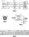
- FIG. 1 a block diagram of a power generator system 10 incorporating a combiner 12.
- the power generator system 10 includes an input amplifier 14, a splitter 16, first and second radio frequency (RF) power amplifiers (PAs) 18, 20, the combiner 12 and a load 22 (e.g., a plasma chamber).
- the input amplifier 14 receives and conditions a RF signal 24 to generate a conditioned signal 26.
- the input amplifier 14 may include, for example, a preamplifier, a driver, etc.
- the splitter 16 provides the conditioned signal 26 to each of the RF PAs 18, 20. Outputs of the splitter 16 may be isolated from each other via an isolator 28.
- the isolator 28 may include one or more resistors and/or other isolating devices.
- the RF PAs 18, 20 may be high-power amplifiers.
- the RF PAs 18, 20 may each provide power outputs of greater than or equal to 2.5 kilowatts (kW).
- the RF PAs 18, 20 generate amplified output signals 30, 32 that are in-phase with each other (e.g., each may have a phase of 0°).
- two RF PAs are shown and number of RF PAs may be incorporated. The number of RF PAs may be odd or even.
- the combiner 12 may be used to combine output signals of other circuit components.
- the combiner 12 combines the amplified output signals 30 and 32 of the RF PAs 18, 20 to provide a power generator output signal 34, which is provided to the load 22.
- the combiner 12 does not provide isolation between output terminals 38, 40 of the RF PAs 18, 20.
- Inputs 42, 44 of the combiner 12 may impedance match outputs of the RF PAs 18, 20.
- output impedance of each of the RF PAs 18, 20 and input impedances of the combiner 12 may each be 50 Ohms ( ⁇ ).
- output impedance of the combiner 12 may match an input impedance of the load 22.
- the output impedance of the combiner 12 and input impedance of the load 22 may each be 50 ⁇ .
- the combiner 12 includes two or more coaxial cables 50, 52 (2 are shown).
- the coaxial cables 50, 52 include coaxial connectors 54, 56, grounding sections 58, 59, a capacitance board 60, and an output connector 62.
- the coaxial cables 50, 52 have coaxial connector (first) ends 64, 66 and capacitor (second) ends 68, 70.
- the coaxial connectors 54, 56 e.g., c-type connectors
- the grounding sections 58, 59 are held by a clamp 72, which is connected to ground 74 (e.g., circuit and/or chassis ground).
- the clamp 72 may be referred to as a grounding clamp.
- the clamp 72 may be, for example, connected and/or screwed to a RF deck, which is grounded or connected to a voltage reference.
- the clamp 72 may be a screw down clamp.
- the second ends 68, 70 are connected to the capacitance board 60.
- the capacitance board 60 is connected to the output connector 62, which in turn may be connected to a load (e.g., load 22).
- the second coaxial cable 52 may have the same cross-sectional make up as the first coaxial cable 50.
- the first coaxial cables 50 may have a core 80 (e.g., a wire), a dielectric insulator 82, a shield 84, and a sheath 86 (designated 80', 82', 84', and 86' respectively for the second coaxial cable 52).
- the core 80 may be connected to and receive an output signal of one of the RF PAs 18, 20, which may be combined to provide the power output signal 34 at the output connector 22.
- the dielectric insulator 82 isolates the core 80 from the shield 84.
- the shield 84 may be, for example, a wire mesh that is exposed and connected to a voltage reference 90 (e.g., a ground reference).
- the core 80 and the shield 84 may be formed of copper or other conductive materials.
- the dielectric insulator 82 and the sheath 86 are non-conductive and may be formed of plastic and/or other dielectric materials.
- Each of the coaxial cables 50, 52 includes four sections; sheathed sections 100, shielded sections 102, non-shielded sections 104, and core sections 106.
- the sheathed sections 100 extend from the coaxial connectors 54, 56 to the clamp 72.
- the shielded sections 102 extend between the sheathed sections 100 and the non-shielded sections 104, are held by the clamp 72 and are connected to the voltage reference 90.
- the sheaths 86, 86' of the coaxial cables 50, 52 are removed to expose the shields 84, 84'.
- the shields 84, 84' are exposed to contact the clamp 72, which couples the shields 84, 84' to the voltage reference 90.
- the non-shielded sections 104 extend from the clamp 72 to the core sections 106.
- the sheaths 86, 86' and the shields 84, 84' are removed from the non-shielded sections 104 to expose the dielectric insulators 82, 82'.
- Each of the non-shielded sections 104 performs as a linear inductor in series with a respective one of the connectors 54, 56. Inductance of each of the non-shielded sections 104 is based on a length D of the non-shielded sections 104. The length D may be selected based on the application.
- the core sections 106 do not include the sheaths 86, 86', the shields 84, 84' and the dielectric insulators 82, 82'.
- the core sections 106 extend from the non-shielded sections 104 and are connected to the capacitance board 60.
- the capacitance board 60 provides a shunt capacitance at the output connector 62 to provide a desired impedance transformation.
- the capacitance board 60 may include any number of capacitors (e.g., capacitors C1, C2), which may be connected in parallel and/or in series. First ends 122 of the capacitors may be connected to the cores 80, 80' in the core sections 106. Second ends 124 of the capacitors may be connected to the voltage reference 90. Output of the capacitance board 60 is provided to the output connector 62.
- capacitors C1, C2 any number of capacitors
- the coaxial cables 50, 52 may have approximately the same dimensions, section lengths, and be formed of the same materials.
- lengths (and other dimensions) of the sheathed sections 100 may be the same
- lengths (and other dimensions) of the shielded sections 102 may be the same
- lengths (and other dimensions) of the non-shielded sections 104 may be the same
- lengths (and other dimensions) of the core sections 106 may be the same. This assures that the impedances and inductances of the coaxial cables 50, 52 are approximately the same.
- the lengths of the non-shielded sections 104 may be approximately the same (e.g., equal in length, which difference between the lengths not greater than ⁇ 1-3 millimeters (mm)), which may match impedances of the non-shielded sections 104 to within, for example, 1 ⁇ .
- the coaxial cables 50, 52 are effectively connected in parallel relative to the second ends 68, 70.
- the output impedance of the combiner 12 e.g., 50 ⁇
- LC inductance and capacitance
- An LC combination is provided by each one of the coaxial cables 50, 52 and corresponding capacitances (e.g., C1, C2).
- a first LC combination is provided by a first non-shielded section of the first coaxial cable 50 and the first capacitance C1.
- a second LC combination is provided by a second non-shielded section of the second coaxial cable 52 and a second capacitance C2.
- each of the capacitances C1 and C2 may include any number of capacitors.
- Each of the LC combinations increases and/or doubles an output impedance of one of the RF PAs 18, 20 (e.g., from 50 ⁇ to 100 ⁇ ).
- the output impedance (e.g., 50 ⁇ ) of the combiner 12 may be approximately equal to (i.e. match) the output impedance of one of the RF PAs 18, 20.
- output impedance of each cable is greater than (or double) the output impedance of each of the RF PAs 18, 20.
- a total output impedance of the combiner 12 may be approximately equal to the output impedance of each of the RF PAs 18, 20.
- the term "approximately equal" to refers to two values being within a predetermined range of each other and/or equal to each other. As an example, the above-stated impedance values may be within ⁇ 1-3 ⁇ of each other.
- the combiner 12 is an inductor-capacitor-inductor (LCL) type combiner.
- Inductances of the non-shielded sections 104 are represented by inductors L1 and L2.
- Total capacitance of the capacitors (e.g., C1 and C2) of the capacitance board 60 is represented by capacitor C Total .
- the inductors L1 and L2 have input ends 150, 152 and output ends 154, 156.
- the capacitor C Total has an input end 158 and an output end 160.
- the input ends 150, 152 may be connected to the coaxial connectors 54, 56 via the sheathed sections 100.
- the output ends 154, 156 are connected to the first end 158 of the capacitor C Total .
- the second end 160 of the capacitor C Total is connected to the voltage reference 90.
- the second end 160 is also connected to the output connector 62.
- the multi-way combiner parameter table provides combiner parameters including total capacitance Total C, non-shielded section inductance L, and non-shielded section length D for various N-way combiners, where N is an integer greater than 1.
- F1-F4 are RF frequencies
- TC1-TC10 are total capacitance values for capacitance C Total
- 11-110 are inductance values for each of inductors L1 and L2
- D1-D10 are length values for length D. Selected total capacitance, inductance and/or length values may decrease relative to an increase in the RF frequency received by the N-way combiners.
- the multi-way combiner parameter table provides example parameter values for 2-way, 3-way and 4-way combiners operating at different frequencies.
- a 2-way combiner refers to a combiner that receives and combines two power outputs from two RF PAs.
- a 2-way combiner is shown in FIGs. 1 , 2 and 4 .
- a 3-way combiner refers to a combiner that receives and combines three power outputs from three RF PAs.
- a 4-way combiner refers to a combiner that receives and combines four power outputs from four RF PAs.
- An N-way combiner that receives 3 or more outputs from 3 or more RF PAs may include an additional coaxial cable and corresponding capacitance for each additional RF PA output received.
- a 3-way combiner may be constructed as the combiner 12 of FIGs. 2 and 4 , but include three LC combinations with three coaxial cables instead of two LC combinations with two coaxial cables.
- the three coaxial cables may be connected effectively in parallel relative to the output connector 62. Any number of coaxial cables and/or LC combinations may be connected to provide a desired power output.
- the total capacitance Total C is the capacitance of the capacitance board or the resulting capacitance of the capacitors (e.g., C Total ) of the LC combinations.
- the non-shielded section inductance L refers to the inductance of each of the non-shielded sections 104 of the combiner 12.
- the inductances of each of the non-shielded sections 104 are based on the lengths of the non-shielded sections (e.g., length D). The lengths may be adjusted based on RF frequencies of amplified RF signals received from RF PAs.
- the inductances (e.g., L1 and L2) of the combiner 12 are provided via the cores 80, 80' of the non-shielded sections 104.
- the inductances are provided without incorporation of additional connectors, printed circuit boards and additional high power inductors.
- the combiner 12 is used to provide, for example, input and output impedance matching of 50 ⁇ .
- the input and output impedance matching may be provided such that impedances of each of the inputs and the combined output of the combiner 12 are 50 ⁇ within, for example, ⁇ 1 ⁇ .
- each output of the RF PAs 18, 20 is connected to a 50 ⁇ load or input impedance of the combiner 12.
- the combiner 12 provides accurate gain and phase matching (e.g., gain within ⁇ 0.1 decibel (dB) and phase within ⁇ 3°) between the coaxial cables 50, 52.
- the phases of the coaxial cables 50, 52 are matched to be combined without signal cancellation.
- each of the coaxial cables 50, 52 of the combiner 12 allows for balanced sharing of power from the RF PAs 18, 20.
- gain matching and phase matching errors of the combiner 12 are less than conventional gain and phase matching errors.
- conventional gain and phase matching errors can be respectively 0.5dB and 10°, which may be magnified by a load of the combiner 12 when the load has a short or open circuit.
- the above-described combiners combine RF power, have minimal sizes and form factors and allow for increased power densities.
- the combiners are formed of coaxial cables, coaxial connectors, and a capacitance board the form factor of the combiner is minimized, without use of a mechanical box, ferrites, transformer windings, etc. This allows the combiners and corresponding RF PAs to be incorporated in a smaller space or footprint than conventional RF PA/combiner systems.
- the structures of the combiners disclosed herein have fewer components and are smaller than conventional high power combiners, the structures are less complex and cost less than conventional high power combiners. By being smaller and less complex, the combiners can be easier to manufacture than conventional combiners.
- the above-disclosed combiners also minimize RF power loss and increases in temperature during operation, as the combiners do not include ferrite materials and/or ferrite transformers.
- the above-disclosed combiners also provide increased reliability due to the inclusion of a minimal number of components and structural complexity.
Landscapes
- Engineering & Computer Science (AREA)
- Power Engineering (AREA)
- Physics & Mathematics (AREA)
- Mathematical Physics (AREA)
- Theoretical Computer Science (AREA)
- Microelectronics & Electronic Packaging (AREA)
- Software Systems (AREA)
- Computer Hardware Design (AREA)
- General Physics & Mathematics (AREA)
- Amplifiers (AREA)
Claims (10)
- Kombinator (12) aufweisend:N Koaxialkabel (50, 52), jedes davon derart gestaltet, dass es an jeweiligen ersten Enden (64, 66) der N Koaxialkabel über einen jeweiligen Koaxialverbinder direkt mit einer jeweiligen Ausgangsklemme (38, 40) von N Radiofrequenzleistungsverstärkern (18, 20) verbunden ist, wobei N eine ganze Zahl größer als eins ist, und wobei jedes der N Koaxialkabel derart gestaltet ist, dass es ein verstärktes Radiofrequenzsignal von einem jeweiligen der N Radiofrequenzleistungsverstärker (18, 20) empfängt;eine Kapazitätsplatte (60) aufweisend eine Mehrzahl von kapazitiven Elementen und derart gestaltet, dass sie mit jedem der N Koaxialkabel an jeweiligen zweiten Enden verbunden ist und die verstärkten Radiofrequenzsignale zusammenfasst/bündelt, wobei die N Koaxialkabel und die Mehrzahl von kapazitiven Elementen N Induktanz- und Kapazitätskombinationen bereitstellen; undeine Ausgangsklemme (62), die derart gestaltet ist, dass sie einen Ausgang der Kapazitätsplatte mit einer Last (22) verbindet, wobei die N Koaxialkabel an zweiten Enden (68, 70) der N Koaxialkabel (50, 52) mit der Kapazitätsplatte verbunden sind.
- Kombinator (12) nach Anspruch 1, wobei die N Koaxialkabel (50, 52) aufweisen:ein erstes Koaxialkabel (50), das derart gestaltet ist, dass es mit einer ersten Ausgangsklemme (38) eines ersten der N Radiofrequenzleistungsverstärker (18) verbunden ist; undein zweites Koaxialkabel (52), das derart gestaltet ist, dass es mit einer zweiten Ausgangsklemme (40) eines zweiten der N Radiofrequenzleistungsverstärker (20) verbunden ist.
- Kombinator (12) nach Anspruch 2, wobei die N Koaxialkabel (50, 52) ferner ein drittes Koaxialkabel, das derart gestaltet ist, dass es mit einer dritten Ausgangsklemme eines dritten der N Radiofrequenzleistungsverstärker verbunden ist, aufweisen.
- Kombinator (12) nach Anspruch 1, wobei:jedes der N Koaxialkabel (50, 52) mit einem jeweiligen der Mehrzahl von kapazitiven Elementen verbunden ist, um eine der N Induktanz- und Kapazitätskombinationen bereitzustellen; undjedes der Mehrzahl von kapazitiven Elementen zwischen die N Koaxialkabel und eine Spannungsreferenz (90) geschaltet ist.
- Kombinator (12) nach Anspruch 1, wobei die Eingangsimpedanz jedes der N Koaxialkabel (50, 52) der Ausgangsimpedanz eines der N Radiofrequenzleistungsverstärker (18, 20) entspricht.
- Kombinator (12) nach Anspruch 1, wobei die Ausgangsimpedanz des Kombinators an dem Verbinder (62) einer Eingangsimpedanz der Last (22) entspricht.
- Kombinator (12) nach Anspruch 1, wobei die N Induktanz- und Kapazitätskombinationen parallel zueinander geschaltet sind.
- Kombinator (12) nach Anspruch 7, wobei:eine Ausgangsimpedanz jedes der N Radiofrequenzleistungsverstärker (18, 20) größer ist als eine Ausgangsimpedanz jeder der N Induktanz- und Kapazitätskombinationen; unddie Ausgangsimpedanz jedes der N Radiofrequenzleistungsverstärker gleich einer gesamten Ausgangsimpedanz des Kombinators ist.
- Kombinator (12) nach Anspruch 1, wobei die N Koaxialkabel (50, 52) hinsichtlich Verstärkung und Phase aufeinander abgestimmt und an der der Last zugeführten Leistung gleichmäßig beteiligt sind.
- Stromerzeugungssystem (10), aufweisend:einen Eingangsverstärker (14), der derart gestaltet ist, dass er ein Radiofrequenzsignal empfängt und ein aufbereitetes Signal erzeugt;einen Verteiler (16), der derart gestaltet ist, dass er das aufbereitete Signal in eine Mehrzahl von Radiofrequenzsignalen aufteilt;die N Radiofrequenzleistungsverstärker (18, 20), die derart gestaltet sind, dass sie die Mehrzahl von Radiofrequenzsignalen verstärken, um die verstärkten Radiofrequenzsignale zu erzeugen; undden Kombinator (12) nach Anspruch 1.
Applications Claiming Priority (3)
| Application Number | Priority Date | Filing Date | Title |
|---|---|---|---|
| US38049610P | 2010-09-07 | 2010-09-07 | |
| US13/222,014 US8791772B2 (en) | 2010-09-07 | 2011-08-31 | LCL high power combiner |
| PCT/US2011/050492 WO2012033729A2 (en) | 2010-09-07 | 2011-09-06 | Lcl high power combiner |
Publications (3)
| Publication Number | Publication Date |
|---|---|
| EP2614554A2 EP2614554A2 (de) | 2013-07-17 |
| EP2614554A4 EP2614554A4 (de) | 2014-04-23 |
| EP2614554B1 true EP2614554B1 (de) | 2018-05-02 |
Family
ID=45770252
Family Applications (1)
| Application Number | Title | Priority Date | Filing Date |
|---|---|---|---|
| EP11823999.5A Not-in-force EP2614554B1 (de) | 2010-09-07 | 2011-09-06 | Hochleistungs-lcl-kombinator |
Country Status (8)
| Country | Link |
|---|---|
| US (2) | US8791772B2 (de) |
| EP (1) | EP2614554B1 (de) |
| JP (1) | JP5889900B2 (de) |
| KR (1) | KR101705606B1 (de) |
| CN (1) | CN103403958B (de) |
| SG (1) | SG187775A1 (de) |
| TW (1) | TWI485923B (de) |
| WO (1) | WO2012033729A2 (de) |
Families Citing this family (9)
| Publication number | Priority date | Publication date | Assignee | Title |
|---|---|---|---|---|
| US9214901B2 (en) * | 2012-07-27 | 2015-12-15 | Mks Instruments, Inc. | Wideband AFT power amplifier systems with frequency-based output transformer impedance balancing |
| JP2014195189A (ja) * | 2013-03-29 | 2014-10-09 | Daihen Corp | 電力合成器および電力分配器 |
| US10224184B2 (en) * | 2014-03-24 | 2019-03-05 | Aes Global Holdings, Pte. Ltd | System and method for control of high efficiency generator source impedance |
| US20160294334A1 (en) * | 2015-03-31 | 2016-10-06 | Cryoelectra Gmbh | Circuit arrangement and apparatus for protecting an electronic component |
| US9871501B2 (en) * | 2015-06-22 | 2018-01-16 | Nxp Usa, Inc. | RF circuit with multiple-definition RF substrate and conductive material void under a bias line |
| CN112444767B (zh) * | 2019-08-30 | 2024-12-03 | 通用电气精准医疗有限责任公司 | 用于磁共振成像的射频功率变换器和射频发射系统 |
| DE102019134463B3 (de) | 2019-12-16 | 2021-05-12 | TRUMPF Hüttinger GmbH + Co. KG | Hochfrequenz-Hochspannungs-Stromleiter-Vorrichtung |
| CN115528404A (zh) * | 2021-06-25 | 2022-12-27 | 广州海格通信集团股份有限公司 | 异频功率合成器和多路异频功率合成器 |
| DE102023111824A1 (de) * | 2023-05-05 | 2024-11-07 | TRUMPF Hüttinger GmbH + Co. KG | HF-Leistungsverstärkereinheit zur Kopplung von HF-Signalen für ein Plasmaprozessversorgungssystem und ein Plasmaprozesssystem |
Citations (2)
| Publication number | Priority date | Publication date | Assignee | Title |
|---|---|---|---|---|
| US6281756B1 (en) * | 1999-07-07 | 2001-08-28 | Mitsubishi Denki Kabushiki Kaisha | Transistor with internal matching circuit |
| US20020079970A1 (en) * | 2000-12-21 | 2002-06-27 | Shigeru Morimoto | RF power amplifier |
Family Cites Families (23)
| Publication number | Priority date | Publication date | Assignee | Title |
|---|---|---|---|---|
| JPS5515881B2 (de) * | 1973-04-17 | 1980-04-26 | ||
| US3963993A (en) | 1975-01-31 | 1976-06-15 | The Bendix Corporation | Power amplifier using a plurality of parallel connected amplifier elements and having burn-out protection |
| JPS5515881A (en) | 1978-07-21 | 1980-02-04 | Pentel Kk | Lettering method and its device |
| JPS57136812A (en) * | 1981-02-17 | 1982-08-24 | Matsushita Electric Ind Co Ltd | High frequency branching synthesizer |
| JPS60254477A (ja) | 1984-05-31 | 1985-12-16 | Fujitsu Ltd | メモリシステム |
| US5206604A (en) * | 1991-12-20 | 1993-04-27 | Harris Corporation | Broadband high power amplifier |
| FI94807C (fi) | 1992-12-30 | 1995-10-25 | Nokia Telecommunications Oy | Menetelmä ja järjestely kompainerisuodattimen virittämiseksi |
| US6252354B1 (en) | 1996-11-04 | 2001-06-26 | Applied Materials, Inc. | RF tuning method for an RF plasma reactor using frequency servoing and power, voltage, current or DI/DT control |
| US5939939A (en) * | 1998-02-27 | 1999-08-17 | Motorola, Inc. | Power combiner with harmonic selectivity |
| JP2000278010A (ja) * | 1999-03-29 | 2000-10-06 | Kokusai Electric Co Ltd | 電力合成器 |
| KR20010037095A (ko) * | 1999-10-13 | 2001-05-07 | 서평원 | 전력증폭기 신호합성용 자동 위상제어 장치 |
| US6887339B1 (en) | 2000-09-20 | 2005-05-03 | Applied Science And Technology, Inc. | RF power supply with integrated matching network |
| US20030117231A1 (en) | 2001-12-21 | 2003-06-26 | Spectrian Corporation | Switched power combiner with adjustable impedance-matching transformer |
| US6707348B2 (en) | 2002-04-23 | 2004-03-16 | Xytrans, Inc. | Microstrip-to-waveguide power combiner for radio frequency power combining |
| US7482894B2 (en) | 2004-02-06 | 2009-01-27 | L-3 Communications Corporation | Radial power divider/combiner using waveguide impedance transformers |
| TWI425767B (zh) | 2005-10-31 | 2014-02-01 | Mks Instr Inc | 無線電頻率電力傳送系統 |
| US7777567B2 (en) | 2007-01-25 | 2010-08-17 | Mks Instruments, Inc. | RF power amplifier stability network |
| US7755452B2 (en) * | 2007-02-27 | 2010-07-13 | Coherent, Inc. | Power combiner |
| EP2215716B1 (de) | 2007-11-19 | 2019-04-24 | Telefonaktiebolaget LM Ericsson (publ) | Zusammengesetzter verstärker, funkendgerät und verfahren zur verbesserung des wirkungsgrads des zusammengesetzten verstärkers |
| US8229043B2 (en) * | 2008-03-21 | 2012-07-24 | Qualcomm Incorporated | Stepped gain mixer |
| US7839223B2 (en) | 2008-03-23 | 2010-11-23 | Advanced Energy Industries, Inc. | Method and apparatus for advanced frequency tuning |
| DE102009051229A1 (de) * | 2009-10-29 | 2011-05-12 | Rohde & Schwarz Gmbh & Co. Kg | Hochfrequenz-Signalkombinierer |
| CN102255127A (zh) * | 2010-05-20 | 2011-11-23 | 上海明珠广播电视科技有限公司 | 一种用于调频大功率多路射频信号的合成器 |
-
2011
- 2011-08-31 US US13/222,014 patent/US8791772B2/en active Active
- 2011-09-02 TW TW100131833A patent/TWI485923B/zh not_active IP Right Cessation
- 2011-09-06 WO PCT/US2011/050492 patent/WO2012033729A2/en not_active Ceased
- 2011-09-06 EP EP11823999.5A patent/EP2614554B1/de not_active Not-in-force
- 2011-09-06 JP JP2013527370A patent/JP5889900B2/ja not_active Expired - Fee Related
- 2011-09-06 CN CN201180042373.XA patent/CN103403958B/zh not_active Expired - Fee Related
- 2011-09-06 SG SG2013009659A patent/SG187775A1/en unknown
- 2011-09-06 KR KR1020137007884A patent/KR101705606B1/ko not_active Expired - Fee Related
-
2014
- 2014-07-28 US US14/444,133 patent/US9477851B2/en not_active Expired - Fee Related
Patent Citations (2)
| Publication number | Priority date | Publication date | Assignee | Title |
|---|---|---|---|---|
| US6281756B1 (en) * | 1999-07-07 | 2001-08-28 | Mitsubishi Denki Kabushiki Kaisha | Transistor with internal matching circuit |
| US20020079970A1 (en) * | 2000-12-21 | 2002-06-27 | Shigeru Morimoto | RF power amplifier |
Also Published As
| Publication number | Publication date |
|---|---|
| WO2012033729A2 (en) | 2012-03-15 |
| TWI485923B (zh) | 2015-05-21 |
| JP5889900B2 (ja) | 2016-03-22 |
| EP2614554A2 (de) | 2013-07-17 |
| KR20130107290A (ko) | 2013-10-01 |
| US8791772B2 (en) | 2014-07-29 |
| US20140333390A1 (en) | 2014-11-13 |
| US20120056658A1 (en) | 2012-03-08 |
| TW201232913A (en) | 2012-08-01 |
| US9477851B2 (en) | 2016-10-25 |
| JP2014507818A (ja) | 2014-03-27 |
| CN103403958A (zh) | 2013-11-20 |
| EP2614554A4 (de) | 2014-04-23 |
| CN103403958B (zh) | 2017-06-20 |
| SG187775A1 (en) | 2013-04-30 |
| WO2012033729A3 (en) | 2012-05-03 |
| KR101705606B1 (ko) | 2017-02-10 |
Similar Documents
| Publication | Publication Date | Title |
|---|---|---|
| EP2614554B1 (de) | Hochleistungs-lcl-kombinator | |
| EP0445139B1 (de) | Einrichtung zur verstärkung mehrerer hochfrequenzsignale | |
| US5982252A (en) | High power broadband non-directional combiner | |
| EP2281321B1 (de) | Leistungsteiler | |
| EP3853875B1 (de) | Hf-leistungsverstärker mit balun-transformator | |
| US6005454A (en) | Radio frequency power divider/combiner circuit having conductive lines and lumped circuits | |
| EP2899803B1 (de) | Schaltung mit Symmetrierglied und Elemente zur Impedanztransformation | |
| EP0200884A2 (de) | Gegentakt-Hochfrequenz-Leistungs-Teilungsaddiergerät | |
| US7683718B2 (en) | Solid-state RF power amplifier for radio transmitters | |
| US9627738B2 (en) | Wideband multilayer transmission line transformer | |
| US6246299B1 (en) | High power broadband combiner having ferrite cores | |
| US20060061431A1 (en) | Broadband transmission line transformer | |
| CN103609019A (zh) | 隔离的零度无功射频高功率合成器 | |
| US5426404A (en) | Electrical circuit using low volume multilayer transmission line devices | |
| US20100301963A1 (en) | Balun with intermediate conductor | |
| CA2676680A1 (en) | Rf re-entrant combiner | |
| CN117353693B (zh) | 一种差分阻抗变换器及电子设备 | |
| US20050040913A1 (en) | Band pass filter | |
| GÜLER et al. | A Four-way Stripline Power Divider Design with Increased Isolation in the 500-1000 MHz Frequency Band | |
| CN119210380A (zh) | 一种射频功率合成器、射频电源及电子设备 | |
| Ta | Compact RF/microwave passive components and modules on multilayer organic substrates | |
| Westberg | AM Antenna Coupling and Phasing Systems |
Legal Events
| Date | Code | Title | Description |
|---|---|---|---|
| PUAI | Public reference made under article 153(3) epc to a published international application that has entered the european phase |
Free format text: ORIGINAL CODE: 0009012 |
|
| 17P | Request for examination filed |
Effective date: 20130405 |
|
| AK | Designated contracting states |
Kind code of ref document: A2 Designated state(s): AL AT BE BG CH CY CZ DE DK EE ES FI FR GB GR HR HU IE IS IT LI LT LU LV MC MK MT NL NO PL PT RO RS SE SI SK SM TR |
|
| DAX | Request for extension of the european patent (deleted) | ||
| A4 | Supplementary search report drawn up and despatched |
Effective date: 20140325 |
|
| RIC1 | Information provided on ipc code assigned before grant |
Ipc: H03F 3/60 20060101ALI20140319BHEP Ipc: H01P 5/12 20060101AFI20140319BHEP Ipc: H01B 9/04 20060101ALI20140319BHEP Ipc: H03F 3/68 20060101ALI20140319BHEP |
|
| 17Q | First examination report despatched |
Effective date: 20170410 |
|
| GRAP | Despatch of communication of intention to grant a patent |
Free format text: ORIGINAL CODE: EPIDOSNIGR1 |
|
| INTG | Intention to grant announced |
Effective date: 20171124 |
|
| GRAS | Grant fee paid |
Free format text: ORIGINAL CODE: EPIDOSNIGR3 |
|
| GRAA | (expected) grant |
Free format text: ORIGINAL CODE: 0009210 |
|
| AK | Designated contracting states |
Kind code of ref document: B1 Designated state(s): AL AT BE BG CH CY CZ DE DK EE ES FI FR GB GR HR HU IE IS IT LI LT LU LV MC MK MT NL NO PL PT RO RS SE SI SK SM TR |
|
| REG | Reference to a national code |
Ref country code: GB Ref legal event code: FG4D |
|
| REG | Reference to a national code |
Ref country code: CH Ref legal event code: EP Ref country code: AT Ref legal event code: REF Ref document number: 996231 Country of ref document: AT Kind code of ref document: T Effective date: 20180515 |
|
| REG | Reference to a national code |
Ref country code: DE Ref legal event code: R096 Ref document number: 602011048111 Country of ref document: DE |
|
| REG | Reference to a national code |
Ref country code: IE Ref legal event code: FG4D |
|
| REG | Reference to a national code |
Ref country code: NL Ref legal event code: MP Effective date: 20180502 |
|
| REG | Reference to a national code |
Ref country code: LT Ref legal event code: MG4D |
|
| PG25 | Lapsed in a contracting state [announced via postgrant information from national office to epo] |
Ref country code: ES Free format text: LAPSE BECAUSE OF FAILURE TO SUBMIT A TRANSLATION OF THE DESCRIPTION OR TO PAY THE FEE WITHIN THE PRESCRIBED TIME-LIMIT Effective date: 20180502 Ref country code: SE Free format text: LAPSE BECAUSE OF FAILURE TO SUBMIT A TRANSLATION OF THE DESCRIPTION OR TO PAY THE FEE WITHIN THE PRESCRIBED TIME-LIMIT Effective date: 20180502 Ref country code: NO Free format text: LAPSE BECAUSE OF FAILURE TO SUBMIT A TRANSLATION OF THE DESCRIPTION OR TO PAY THE FEE WITHIN THE PRESCRIBED TIME-LIMIT Effective date: 20180802 Ref country code: LT Free format text: LAPSE BECAUSE OF FAILURE TO SUBMIT A TRANSLATION OF THE DESCRIPTION OR TO PAY THE FEE WITHIN THE PRESCRIBED TIME-LIMIT Effective date: 20180502 Ref country code: FI Free format text: LAPSE BECAUSE OF FAILURE TO SUBMIT A TRANSLATION OF THE DESCRIPTION OR TO PAY THE FEE WITHIN THE PRESCRIBED TIME-LIMIT Effective date: 20180502 Ref country code: BG Free format text: LAPSE BECAUSE OF FAILURE TO SUBMIT A TRANSLATION OF THE DESCRIPTION OR TO PAY THE FEE WITHIN THE PRESCRIBED TIME-LIMIT Effective date: 20180802 |
|
| PG25 | Lapsed in a contracting state [announced via postgrant information from national office to epo] |
Ref country code: GR Free format text: LAPSE BECAUSE OF FAILURE TO SUBMIT A TRANSLATION OF THE DESCRIPTION OR TO PAY THE FEE WITHIN THE PRESCRIBED TIME-LIMIT Effective date: 20180803 Ref country code: RS Free format text: LAPSE BECAUSE OF FAILURE TO SUBMIT A TRANSLATION OF THE DESCRIPTION OR TO PAY THE FEE WITHIN THE PRESCRIBED TIME-LIMIT Effective date: 20180502 Ref country code: NL Free format text: LAPSE BECAUSE OF FAILURE TO SUBMIT A TRANSLATION OF THE DESCRIPTION OR TO PAY THE FEE WITHIN THE PRESCRIBED TIME-LIMIT Effective date: 20180502 Ref country code: LV Free format text: LAPSE BECAUSE OF FAILURE TO SUBMIT A TRANSLATION OF THE DESCRIPTION OR TO PAY THE FEE WITHIN THE PRESCRIBED TIME-LIMIT Effective date: 20180502 Ref country code: HR Free format text: LAPSE BECAUSE OF FAILURE TO SUBMIT A TRANSLATION OF THE DESCRIPTION OR TO PAY THE FEE WITHIN THE PRESCRIBED TIME-LIMIT Effective date: 20180502 |
|
| REG | Reference to a national code |
Ref country code: AT Ref legal event code: MK05 Ref document number: 996231 Country of ref document: AT Kind code of ref document: T Effective date: 20180502 |
|
| PG25 | Lapsed in a contracting state [announced via postgrant information from national office to epo] |
Ref country code: CZ Free format text: LAPSE BECAUSE OF FAILURE TO SUBMIT A TRANSLATION OF THE DESCRIPTION OR TO PAY THE FEE WITHIN THE PRESCRIBED TIME-LIMIT Effective date: 20180502 Ref country code: RO Free format text: LAPSE BECAUSE OF FAILURE TO SUBMIT A TRANSLATION OF THE DESCRIPTION OR TO PAY THE FEE WITHIN THE PRESCRIBED TIME-LIMIT Effective date: 20180502 Ref country code: SK Free format text: LAPSE BECAUSE OF FAILURE TO SUBMIT A TRANSLATION OF THE DESCRIPTION OR TO PAY THE FEE WITHIN THE PRESCRIBED TIME-LIMIT Effective date: 20180502 Ref country code: DK Free format text: LAPSE BECAUSE OF FAILURE TO SUBMIT A TRANSLATION OF THE DESCRIPTION OR TO PAY THE FEE WITHIN THE PRESCRIBED TIME-LIMIT Effective date: 20180502 Ref country code: AT Free format text: LAPSE BECAUSE OF FAILURE TO SUBMIT A TRANSLATION OF THE DESCRIPTION OR TO PAY THE FEE WITHIN THE PRESCRIBED TIME-LIMIT Effective date: 20180502 Ref country code: PL Free format text: LAPSE BECAUSE OF FAILURE TO SUBMIT A TRANSLATION OF THE DESCRIPTION OR TO PAY THE FEE WITHIN THE PRESCRIBED TIME-LIMIT Effective date: 20180502 Ref country code: EE Free format text: LAPSE BECAUSE OF FAILURE TO SUBMIT A TRANSLATION OF THE DESCRIPTION OR TO PAY THE FEE WITHIN THE PRESCRIBED TIME-LIMIT Effective date: 20180502 |
|
| REG | Reference to a national code |
Ref country code: DE Ref legal event code: R097 Ref document number: 602011048111 Country of ref document: DE |
|
| PG25 | Lapsed in a contracting state [announced via postgrant information from national office to epo] |
Ref country code: IT Free format text: LAPSE BECAUSE OF FAILURE TO SUBMIT A TRANSLATION OF THE DESCRIPTION OR TO PAY THE FEE WITHIN THE PRESCRIBED TIME-LIMIT Effective date: 20180502 Ref country code: SM Free format text: LAPSE BECAUSE OF FAILURE TO SUBMIT A TRANSLATION OF THE DESCRIPTION OR TO PAY THE FEE WITHIN THE PRESCRIBED TIME-LIMIT Effective date: 20180502 |
|
| PLBE | No opposition filed within time limit |
Free format text: ORIGINAL CODE: 0009261 |
|
| STAA | Information on the status of an ep patent application or granted ep patent |
Free format text: STATUS: NO OPPOSITION FILED WITHIN TIME LIMIT |
|
| 26N | No opposition filed |
Effective date: 20190205 |
|
| PG25 | Lapsed in a contracting state [announced via postgrant information from national office to epo] |
Ref country code: MC Free format text: LAPSE BECAUSE OF FAILURE TO SUBMIT A TRANSLATION OF THE DESCRIPTION OR TO PAY THE FEE WITHIN THE PRESCRIBED TIME-LIMIT Effective date: 20180502 |
|
| REG | Reference to a national code |
Ref country code: CH Ref legal event code: PL |
|
| GBPC | Gb: european patent ceased through non-payment of renewal fee |
Effective date: 20180906 |
|
| PG25 | Lapsed in a contracting state [announced via postgrant information from national office to epo] |
Ref country code: SI Free format text: LAPSE BECAUSE OF FAILURE TO SUBMIT A TRANSLATION OF THE DESCRIPTION OR TO PAY THE FEE WITHIN THE PRESCRIBED TIME-LIMIT Effective date: 20180502 |
|
| REG | Reference to a national code |
Ref country code: BE Ref legal event code: MM Effective date: 20180930 |
|
| REG | Reference to a national code |
Ref country code: IE Ref legal event code: MM4A |
|
| PG25 | Lapsed in a contracting state [announced via postgrant information from national office to epo] |
Ref country code: LU Free format text: LAPSE BECAUSE OF NON-PAYMENT OF DUE FEES Effective date: 20180906 |
|
| PG25 | Lapsed in a contracting state [announced via postgrant information from national office to epo] |
Ref country code: IE Free format text: LAPSE BECAUSE OF NON-PAYMENT OF DUE FEES Effective date: 20180906 |
|
| PG25 | Lapsed in a contracting state [announced via postgrant information from national office to epo] |
Ref country code: LI Free format text: LAPSE BECAUSE OF NON-PAYMENT OF DUE FEES Effective date: 20180930 Ref country code: FR Free format text: LAPSE BECAUSE OF NON-PAYMENT OF DUE FEES Effective date: 20180930 Ref country code: BE Free format text: LAPSE BECAUSE OF NON-PAYMENT OF DUE FEES Effective date: 20180930 Ref country code: CH Free format text: LAPSE BECAUSE OF NON-PAYMENT OF DUE FEES Effective date: 20180930 |
|
| PG25 | Lapsed in a contracting state [announced via postgrant information from national office to epo] |
Ref country code: GB Free format text: LAPSE BECAUSE OF NON-PAYMENT OF DUE FEES Effective date: 20180906 |
|
| PG25 | Lapsed in a contracting state [announced via postgrant information from national office to epo] |
Ref country code: AL Free format text: LAPSE BECAUSE OF FAILURE TO SUBMIT A TRANSLATION OF THE DESCRIPTION OR TO PAY THE FEE WITHIN THE PRESCRIBED TIME-LIMIT Effective date: 20180502 |
|
| PG25 | Lapsed in a contracting state [announced via postgrant information from national office to epo] |
Ref country code: MT Free format text: LAPSE BECAUSE OF NON-PAYMENT OF DUE FEES Effective date: 20180906 |
|
| PG25 | Lapsed in a contracting state [announced via postgrant information from national office to epo] |
Ref country code: TR Free format text: LAPSE BECAUSE OF FAILURE TO SUBMIT A TRANSLATION OF THE DESCRIPTION OR TO PAY THE FEE WITHIN THE PRESCRIBED TIME-LIMIT Effective date: 20180502 |
|
| PG25 | Lapsed in a contracting state [announced via postgrant information from national office to epo] |
Ref country code: PT Free format text: LAPSE BECAUSE OF FAILURE TO SUBMIT A TRANSLATION OF THE DESCRIPTION OR TO PAY THE FEE WITHIN THE PRESCRIBED TIME-LIMIT Effective date: 20180502 Ref country code: HU Free format text: LAPSE BECAUSE OF FAILURE TO SUBMIT A TRANSLATION OF THE DESCRIPTION OR TO PAY THE FEE WITHIN THE PRESCRIBED TIME-LIMIT; INVALID AB INITIO Effective date: 20110906 |
|
| PG25 | Lapsed in a contracting state [announced via postgrant information from national office to epo] |
Ref country code: MK Free format text: LAPSE BECAUSE OF NON-PAYMENT OF DUE FEES Effective date: 20180502 Ref country code: CY Free format text: LAPSE BECAUSE OF FAILURE TO SUBMIT A TRANSLATION OF THE DESCRIPTION OR TO PAY THE FEE WITHIN THE PRESCRIBED TIME-LIMIT Effective date: 20180502 |
|
| PG25 | Lapsed in a contracting state [announced via postgrant information from national office to epo] |
Ref country code: IS Free format text: LAPSE BECAUSE OF FAILURE TO SUBMIT A TRANSLATION OF THE DESCRIPTION OR TO PAY THE FEE WITHIN THE PRESCRIBED TIME-LIMIT Effective date: 20180902 |
|
| PGFP | Annual fee paid to national office [announced via postgrant information from national office to epo] |
Ref country code: DE Payment date: 20230927 Year of fee payment: 13 |
|
| REG | Reference to a national code |
Ref country code: DE Ref legal event code: R119 Ref document number: 602011048111 Country of ref document: DE |
|
| PG25 | Lapsed in a contracting state [announced via postgrant information from national office to epo] |
Ref country code: DE Free format text: LAPSE BECAUSE OF NON-PAYMENT OF DUE FEES Effective date: 20250401 |