EP2613486A2 - Niedervolt-Leitungstreiber - Google Patents
Niedervolt-Leitungstreiber Download PDFInfo
- Publication number
- EP2613486A2 EP2613486A2 EP12008386.0A EP12008386A EP2613486A2 EP 2613486 A2 EP2613486 A2 EP 2613486A2 EP 12008386 A EP12008386 A EP 12008386A EP 2613486 A2 EP2613486 A2 EP 2613486A2
- Authority
- EP
- European Patent Office
- Prior art keywords
- differential
- differential output
- current
- voltage
- nodes
- Prior art date
- Legal status (The legal status is an assumption and is not a legal conclusion. Google has not performed a legal analysis and makes no representation as to the accuracy of the status listed.)
- Granted
Links
Images



Classifications
-
- H—ELECTRICITY
- H04—ELECTRIC COMMUNICATION TECHNIQUE
- H04L—TRANSMISSION OF DIGITAL INFORMATION, e.g. TELEGRAPHIC COMMUNICATION
- H04L25/00—Baseband systems
- H04L25/02—Details ; arrangements for supplying electrical power along data transmission lines
- H04L25/0264—Arrangements for coupling to transmission lines
- H04L25/0272—Arrangements for coupling to multiple lines, e.g. for differential transmission
-
- H—ELECTRICITY
- H04—ELECTRIC COMMUNICATION TECHNIQUE
- H04L—TRANSMISSION OF DIGITAL INFORMATION, e.g. TELEGRAPHIC COMMUNICATION
- H04L25/00—Baseband systems
- H04L25/02—Details ; arrangements for supplying electrical power along data transmission lines
-
- H—ELECTRICITY
- H03—ELECTRONIC CIRCUITRY
- H03K—PULSE TECHNIQUE
- H03K19/00—Logic circuits, i.e. having at least two inputs acting on one output; Inverting circuits
- H03K19/0175—Coupling arrangements; Interface arrangements
-
- H—ELECTRICITY
- H04—ELECTRIC COMMUNICATION TECHNIQUE
- H04L—TRANSMISSION OF DIGITAL INFORMATION, e.g. TELEGRAPHIC COMMUNICATION
- H04L25/00—Baseband systems
- H04L25/02—Details ; arrangements for supplying electrical power along data transmission lines
- H04L25/0264—Arrangements for coupling to transmission lines
- H04L25/028—Arrangements specific to the transmitter end
Definitions
- This disclosure relates to line drivers for communication networks.
- this disclosure relates to a low voltage line driver for communication networks such as Ethernet networks.
- Line drivers typically transmit information across a network transmission line by generating a differential output voltage responsive to an input signal.
- Line drivers also provide a termination impedance, typically 100 ohms, for the network transmission line.
- the termination impedance is sometimes implemented either as an actual resistor (e.g., a physical 100 ohm resistor), or, more commonly, as an active termination stage in which a complex active circuit simulates a resistor.
- There is a need for a new active termination architecture that is suitable for smaller scale manufacturing processes (e.g., 28 nm processes) for circuits that use lower voltage supplies (e.g., 1.8 V).
- a line driver comprises:
- the circuitry comprises:
- the line driver further comprises:
- the transconductance stage further comprises:
- the line driver further comprises:
- At least one of the differential input nodes is coupled to an amplifier input that is also coupled to at least one of the differential input nodes.
- a method for driving a communication line comprising:
- the method further comprises:
- the method further comprises:
- the method further comprises:
- the method further comprises:
- the method further comprises:
- the method further comprises:
- a line driver comprises:
- the first current mirror comprises:
- the mirror transistor comprises a geometry with respect to the diode-connected transistor that implements a selected mirroring ratio.
- the transconductance stage further comprises:
- the line driver further comprises:
- the differential input nodes comprise:
- Figure 1 shows a prior art line driver in which the active termination circuitry is stacked under the output nodes.
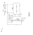
- Figure 2 shows a new line driver
- FIG. 3 shows a detailed circuit diagram of the new line driver.
- Figure 4 shows an alternative implementation of a line driver.
- Figure 5 shows an alternative implementation of a line driver.
- Figure 6 shows an alternative implementation of a line driver.
- Figure 7 shows a flow diagram of a technique to transmit data over communication lines.
- FIG. 1 shows a prior art line driver 100 in which a transconductance stage 102 is stacked under the differential output nodes tdp 104 and tdn 106.
- an active termination circuit 108 may simulate a physical resistance of 100 ohms between the differential output nodes 104 and 106. To that end, the active termination circuit 108 may sense the voltage on the differential output nodes 104 and 106 and directly produce a current equal to the difference in voltage divided by 100 ohms through the differential output nodes 104 and 106.
- the circuitry in the active termination circuit 108 is stacked below the differential output nodes 104 and 106.
- the circuitry in the active termination circuit 108 sits below (e.g., in series with) the differential output nodes 104 and 106, and produces differential current directly into the differential output nodes 104 and 106 through the transistors connected to the amplifier outputs.
- a somewhat higher line driver voltage supply e.g., 2.5 V is used to bias the differential output nodes 104 and 106 and to provide sufficient headroom for the active termination circuit 108 to function properly.
- Figure 2 shows a line driver 200 that may operate with a reduced line driver voltage supply, such as 1.8 V, for example.
- the line driver 200 separates or decouples the transconductance stage 202 from being stacked under the differential output nodes 104 and 106.
- the line driver 200 does not produce current directly into the differential output nodes 104 and 106. Instead, the transconductance stage 202 produces a local differential current, and the current transfer stage 206 (e.g., a current mirror) generates a corresponding differential current in the differential output nodes 104 and 106.
- the current transfer stage 206 e.g., a current mirror
- the transconductance stage 202 may be powered directly by the same or by a separate voltage source that supplies the line driver supply voltage to the differential output nodes 104 and 106.
- the transconductance stage 202 including amplifiers and other circuit components (or any other circuitry configured to drive the differential output nodes 104, 106), may be powered directly from the chip voltage supply 204 (e.g., a 1.8 V supply).
- the chip voltage supply 204 is connected to the transconductance stage 202 through a transconductance stage voltage supply input 212.
- the transconductance stage 202 is not stacked under the differential output nodes 104 and 106 and does not need to operate with the reduced voltage headroom caused by such a configuration.
- the transconductance stage 202 is decoupled from operation using the reduced voltage headroom and may correctly operate using the full range of the lower supply voltage (e.g., 1.8 V), where it would be difficult or impossible to operate using the reduced headroom range (e.g., 550 mV) that would result from being stacked under the differential output nodes 104 and 106.
- the transconductance stage 202 is no longer limited in its operational voltage range by the voltage ranges present on the differential output nodes 104 and 106.
- the differential output nodes 104 and 106 may be output pins or pads on a physical line driver integrated circuit package that includes the line driver 200.
- the differential output nodes 104 and 106 are connected through an off-chip transformer 208.
- a tap 210 e.g., a center tap
- the transformer 208 may be part of a transformer circuit that isolates the differential output nodes 104 and 106 from the physical differential output lines that interconnect different devices, systems, or networks. The transformer circuit reproduces the voltage differential across the differential output nodes 104 and 106 onto the actual differential output lines being driven.
- the transconductance stage 202 senses the voltage difference Vtdp - Vtdn, and generates a current responsive to the voltage difference. For example, for a 100 ohm active termination, the transconductance stage 202 generates a current that, after the current transfer stage 206, is approximately (Vtdp - Vtdn) / 100 through the differential output nodes 104 and 106.
- the current transfer stage 206 e.g., a current mirror
- the transconductance stage 202 implements a relatively low current (less than the full desired output current through the differential output nodes 104 and 106), while the current transfer stage 206 implements a current gain to achieve that desired current through the differential output nodes 104 and 106.
- the current gain in the current transfer stage need not be 1:1, but may instead be set to achieve a desired power efficiency in the transconductance stage 202.
- the transconductance stage 202 is an active termination stage.
- the active termination stage may employ operational amplifiers that control transistors based on voltage sensing resistor networks, with a feedback loop.
- the current transfer stage 206 replicates the current generated in the transconductance stage to the differential output nodes 104 and 106 in an amount needed to provide the desired termination impedance.
- the transconductance stage 202 may be implemented in other ways than as an active termination circuit, however, and the current transfer stage 206 may be implemented in other ways than as a current mirror.
- FIG 3 shows a detailed circuit diagram 300 of the line driver 200.
- the line driver includes differential output nodes 104 and 106.
- the differential output nodes 104 and 106 may connect through an off-chip transformer 302 that has a center tap 304.
- the center tap 304 provides a line driver voltage supply input to which is connected a line driver supply voltage (e.g., 1.8V).
- a line driver supply voltage e.g., 1.8V
- a transconductance stage 306 is coupled to the differential output nodes 104 and 106.
- the transconductance stage 306 includes a transconductance stage voltage supply input (connected, for example, to the chip voltage supply 204) and that may be separate or the same as the line driver voltage supply input.
- the transconductance stage 306, in this example, is an active termination stage for the differential output nodes 104 and 106.
- the active termination stage senses a differential voltage on the differential output nodes 104 and 106 and produces a differential output current that (as explained in more detail below) will match to the desired impedance (e.g., 100 ohms) across the differential output nodes 104 and 106, when the differential output current is mirrored to the differential output nodes 104 and 106.
- a transconductance output 308 of the active termination stage carries the differential output current corresponding to the differential voltage.
- the differential output current flows through the drain connection 310 of the Mgm1 transistor and the drain connection 312 of the Mgm2 transistor.
- the differential output current is not provided directly into the differential output nodes 104 and 106.
- a current mirror stage 314 is connected to the differential output nodes 104 and 106 and the transconductance output 308.
- the current mirror stage 314 generates (e.g., by current mirroring) a version of the differential output current to the differential output nodes 104 and 106.
- the current mirror formed by M2in and M2out mirrors, to the differential output node tdn the part of the differential output current flowing through the drain connection 312.
- the line driver 300 also includes differential input nodes 316 (Isig_p) and 318 (Isig_n).
- the differential input nodes 3165 and 318 force current to generate a specified output voltage at the differential output nodes 104 and 106.
- the differential input nodes 316 and 318 are coupled to the non-inverting operational amplifier nodes 320 and 322, respectively.
- the currents forced on the differential input nodes 316 and 318 change the voltage present at the non-inverting operation amplifier input nodes 320 and 322, and thus the output voltages at the differential output nodes 104 and 106.
- the transconductance stage 306 produces a corresponding change in current at the transconductance output 308, and the current mirror stage 314 generates a corresponding current in the differential output nodes 104 and 106, to maintain the desired active termination impedance.
- the transconductance stage 306 includes operational amplifiers 325 and 327 with amplifier input stages 324 and 326.
- the operational amplifiers 325 and 327 replicate a fraction of the differential voltage present on the differential output nodes 104 and 106 at the source nodes of the Mgm1 and Mgm2 transistors included in the amplifier output stages 328 and 330.
- the amplifier output stages 328 and 330 generate the differential output current in the transconductance output 308.
- the transconductance stage 306 senses the differential voltage present on the differential output nodes 104 and 106 using the voltage sensing networks coupled to the non-inverting inputs of the operational amplifiers.
- the voltage sensing networks form a negative feedback loop for each operational amplifier.
- the voltage sensing networks are implemented as voltage dividers formed from R1 and R2.
- the values of R1 and R2 may vary widely. In one implementation, the value of R1 is approximately 1 K ohms and the value of R2 is approximately 10K ohms.
- the transconductance stage 306 presents a scaled version (as set by R1 and R2) of the differential voltage present at the differential output nodes 104 and 106 across the tail resistors Rt.
- the tail resistors Rt divide the tail current Itail to form the differential output current flowing through the drain connection 310 of the Mgm1 transistor and the drain connection 312 of the Mgm2 transistor.
- the tail resistors Rt may vary in resistance according to the desired impedance that the transconductance stage 306 presents. In one implementation, the tail resistors Rt are approximately 5 ohms or less. However, the resistance of the tail resistors Rt can be adjusted for ease of fabrication or manufacturing by, for example, changing the gain in the current mirror stage 314.
- the component values and impedance, Z, presented by the line driver 300 are related by:
- k is the mirroring ratio (e.g., the gain in the current mirror stage 314) between M1in, M2in, M1out, and M2out (e.g., between 1:4 and 1:10).
- a differential voltage on the differential output nodes 104 and 106 is divided by resistors R1 and R2 and coupled to the non-inverting inputs of the operational amplifiers.
- the negative feedback of the operational amplifiers, along with the transistors Mgm1 and Mgm2 replicate a scaled version of the differential voltage across the tail resistors Rt.
- the scaled version of the differential voltage produces a differential current local to the transconductance stage 306.
- the current mirror 314 then mirrors the differential current, using the transistor pairs M1in and M1out, M2in and M2out, to the differential output nodes 104 and 106, to maintain the desired termination impedance.
- Figure 4 shows an alternative example of a line driver 400.
- the signal current Isig_n 318 and Isig_p 316 is supplied or removed at the mirroring nodes of the M1in and M2in transistors.
- the signal current is added or removed at the base connection of the M1in and M2in transistors, which are configured as diodes.
- FIG. 5 shows another alternative implementation of a line driver 500, and in particular a line driver with a different transconductance stage than the one described above.
- a transconductance stage 502 feeds a current mirror 504.
- the differential output nodes txp 506 and txm 508 are not stacked above the transconductance stage 502. Instead, the transconductance stage 502 generates a differential current appropriate for providing the desired output impedance across the differential output nodes 506 and 508.
- the differential output current flows through the transconductance output 510 (e.g., the drain connections of the diode connected transistors T1 and T2).
- the current mirror 504 then produces a differential current in the differential output nodes 506 and 508 to achieve the desired termination impedance.
- a differential input current is forced on the differential input nodes 512 (ip) and 514 (im) to generate a desired differential output at the differential output nodes 506 and 508.
- Figure 6 shows another alternative implementation of a line driver 600, and in particular a line driver with a different transconductance stage than the ones described above. Similar to the designs explained above, in the line driver 600 a transconductance stage 602 feeds a current mirror 604. The differential output nodes txp 606 and txm 608 are not stacked above the transconductance stage 602. Instead, the transconductance stage 602 generates a differential current appropriate for providing the desired output impedance across the differential output nodes 606 and 608. The differential output current flows through the transconductance output 610 (e.g., the drain connections of the diode connected transistors T1 and T2).
- the transconductance output 610 e.g., the drain connections of the diode connected transistors T1 and T2.
- the current mirror 604 then produces a differential current in the differential output nodes 606 and 608 to achieve the desired termination impedance.
- a differential input current is forced on the differential input nodes 612 (ip) and 614 (im) to generate a desired differential output at the differential output nodes 606 and 608.
- Figure 7 shows a method 700 for driving a communication line.
- a line driver is provided in which the transconductance stage is not stacked under the differential output nodes (702).
- the transconductance stage senses a differential voltage present on differential output nodes (704).
- the transconductance stage generates a differential output current corresponding to the differential voltage on the differential output nodes at a transconductance output (706).
- the differential output current implements a desired output impedance (e.g., 100 ohms) across the differential output nodes.
- the transconductance stage may implement an active termination (e.g., to give the appearance of the desired output impedance) of the differential output nodes.
- a current mirror stage connected to the transconductance output receives the differential output current.
- the current mirror stage mirrors the differential output current to the differential output nodes (708).
- differential inputs may force differential current to the transconductance stage (710).
- the differential current may be forced at the non-inverting inputs of the operational amplifiers 325 and 327, or at the diode connected transistors M1in and M2in, as shown in Figures 3 and 4 . This operation continues for as long as desired.
- the new line drivers described above substantially decouple the transconductance stages from the differential output nodes, other than sensing the differential voltage across the differential output nodes, and mirroring a differential current (generated in the transconductance stage) back to the differential output nodes.
- the present line drivers permit lowering the voltage supply (e.g., the center tap voltage) to 1.8V.
- the reduced voltage supply results in a system power reduction by as much as 28% or more.
- a 1.8V supply is typically available in 28 nm products, and using the available 1.8V supply eliminates the requirement to generate (e.g., with additional circuitry) a separate 2.5V supply. Furthermore, the 1.8V supply is compatible with the voltage tolerances of thick oxide transistors used in the 28 nm process, which means that special transistor designs (or other circuit overhead to avoid overvoltage situations) are not needed as they would be if a 2.5V supply was used for the line driver.
Landscapes
- Engineering & Computer Science (AREA)
- Power Engineering (AREA)
- Computer Networks & Wireless Communication (AREA)
- Signal Processing (AREA)
- Computer Hardware Design (AREA)
- Physics & Mathematics (AREA)
- Computing Systems (AREA)
- General Engineering & Computer Science (AREA)
- Mathematical Physics (AREA)
- Amplifiers (AREA)
- Dc Digital Transmission (AREA)
- Logic Circuits (AREA)
Applications Claiming Priority (1)
| Application Number | Priority Date | Filing Date | Title |
|---|---|---|---|
| US13/338,122 US8760198B2 (en) | 2011-12-27 | 2011-12-27 | Low voltage line driver |
Publications (3)
| Publication Number | Publication Date |
|---|---|
| EP2613486A2 true EP2613486A2 (de) | 2013-07-10 |
| EP2613486A3 EP2613486A3 (de) | 2016-04-20 |
| EP2613486B1 EP2613486B1 (de) | 2017-02-22 |
Family
ID=47562919
Family Applications (1)
| Application Number | Title | Priority Date | Filing Date |
|---|---|---|---|
| EP12008386.0A Active EP2613486B1 (de) | 2011-12-27 | 2012-12-17 | Niedervolt-Leitungstreiber |
Country Status (5)
| Country | Link |
|---|---|
| US (1) | US8760198B2 (de) |
| EP (1) | EP2613486B1 (de) |
| KR (1) | KR101476416B1 (de) |
| CN (1) | CN103188178B (de) |
| TW (1) | TWI477118B (de) |
Families Citing this family (3)
| Publication number | Priority date | Publication date | Assignee | Title |
|---|---|---|---|---|
| WO2017098951A1 (ja) * | 2015-12-11 | 2017-06-15 | ソニー株式会社 | 送受信装置、および送受信方法、並びにプログラム |
| EP3270518B1 (de) * | 2016-07-14 | 2019-08-07 | Intel IP Corporation | Zeitduplex-empfänger mit konstanter impedanz für ein breitbandiges leitungsendgerät mit asynchroner übertragung |
| DE102018007144B4 (de) * | 2018-09-10 | 2019-10-10 | Inova Semiconductors Gmbh | Leitungstreibervorrichtung zur Datenflusskontrolle |
Family Cites Families (6)
| Publication number | Priority date | Publication date | Assignee | Title |
|---|---|---|---|---|
| DE69523281T2 (de) * | 1995-02-10 | 2002-07-11 | Alcatel, Paris | Linearer abstimmbarer Gm-C Integrator |
| US6483380B1 (en) * | 2000-09-18 | 2002-11-19 | Conexant Systems, Inc. | GMC filter and method for suppressing unwanted signals introduced by the filter |
| EP1332590A2 (de) | 2000-10-26 | 2003-08-06 | Broadcom Corporation | Leitungstreiber mit schutz gegen rückführung |
| US6686772B2 (en) * | 2001-11-19 | 2004-02-03 | Broadcom Corporation | Voltage mode differential driver and method |
| US6617888B2 (en) * | 2002-01-02 | 2003-09-09 | Intel Corporation | Low supply voltage differential signal driver |
| TW200412018A (en) | 2002-12-18 | 2004-07-01 | Realtek Semiconductor Corp | Line driver with active termination |
-
2011
- 2011-12-27 US US13/338,122 patent/US8760198B2/en active Active
-
2012
- 2012-12-10 TW TW101146386A patent/TWI477118B/zh not_active IP Right Cessation
- 2012-12-17 EP EP12008386.0A patent/EP2613486B1/de active Active
- 2012-12-27 CN CN201210581307.6A patent/CN103188178B/zh active Active
- 2012-12-27 KR KR1020120155082A patent/KR101476416B1/ko not_active Expired - Fee Related
Non-Patent Citations (1)
| Title |
|---|
| None |
Also Published As
| Publication number | Publication date |
|---|---|
| TWI477118B (zh) | 2015-03-11 |
| KR20130075711A (ko) | 2013-07-05 |
| US8760198B2 (en) | 2014-06-24 |
| HK1184290A1 (zh) | 2014-01-17 |
| CN103188178A (zh) | 2013-07-03 |
| TW201330555A (zh) | 2013-07-16 |
| EP2613486A3 (de) | 2016-04-20 |
| US20130162301A1 (en) | 2013-06-27 |
| CN103188178B (zh) | 2016-08-03 |
| EP2613486B1 (de) | 2017-02-22 |
| KR101476416B1 (ko) | 2014-12-24 |
Similar Documents
| Publication | Publication Date | Title |
|---|---|---|
| CN107102669B (zh) | 用于芯片上驱动和管芯上端接的校准电路 | |
| JP3202728B2 (ja) | バックプレーン適用用のlvdsドライバ | |
| US7635990B1 (en) | Methods and apparatus for implementing an output circuit | |
| US6891357B2 (en) | Reference current generation system and method | |
| EP1318601B1 (de) | Differenztreiberstufe mit Spannungssteuerung und Verfahren | |
| US9111602B2 (en) | Accurate global reference voltage distribution system with local reference voltages referred to local ground and locally supplied voltage | |
| US20020190754A1 (en) | Low voltage differential signaling circuit with mid-point bias | |
| TWI593232B (zh) | 單端可建置式多模式驅動器 | |
| US7528636B2 (en) | Low differential output voltage circuit | |
| CN107066416B (zh) | 串行通信系统的驱动电路及驱动方法 | |
| JP3723317B2 (ja) | 信号伝送に用いる駆動回路、バイアス発生回路 | |
| TWI445300B (zh) | 具有寬廣動態範圍的平方單元及實施平方單元的電力偵測器 | |
| US8760198B2 (en) | Low voltage line driver | |
| US20060170461A1 (en) | Comparator circuit having reduced pulse width distortion | |
| JPH10500808A (ja) | 信号受信・処理ユニット | |
| US7504863B2 (en) | Half-duplex communication system, low-voltage differential signaling transceiver of the system and pre-driver of the transceiver | |
| JP2008005196A (ja) | 出力インピーダンス調整回路、半導体装置及び出力インピーダンス調整方法 | |
| US5680037A (en) | High accuracy current mirror | |
| US6900686B1 (en) | Analog switching circuit | |
| US7528637B2 (en) | Driver circuit | |
| US10700652B2 (en) | Ethernet line driver | |
| CN102915701A (zh) | 用于led通道的电流匹配的系统和方法 | |
| HK1184290B (en) | Low voltage line driver | |
| CN100353666C (zh) | 在隔离系统之间的电平移动电路 | |
| US7659755B1 (en) | Method and apparatus including a driver for driving a floating bipolar switch |
Legal Events
| Date | Code | Title | Description |
|---|---|---|---|
| PUAI | Public reference made under article 153(3) epc to a published international application that has entered the european phase |
Free format text: ORIGINAL CODE: 0009012 |
|
| 17P | Request for examination filed |
Effective date: 20121217 |
|
| AK | Designated contracting states |
Kind code of ref document: A2 Designated state(s): AL AT BE BG CH CY CZ DE DK EE ES FI FR GB GR HR HU IE IS IT LI LT LU LV MC MK MT NL NO PL PT RO RS SE SI SK SM TR |
|
| AX | Request for extension of the european patent |
Extension state: BA ME |
|
| PUAL | Search report despatched |
Free format text: ORIGINAL CODE: 0009013 |
|
| AK | Designated contracting states |
Kind code of ref document: A3 Designated state(s): AL AT BE BG CH CY CZ DE DK EE ES FI FR GB GR HR HU IE IS IT LI LT LU LV MC MK MT NL NO PL PT RO RS SE SI SK SM TR |
|
| AX | Request for extension of the european patent |
Extension state: BA ME |
|
| RIC1 | Information provided on ipc code assigned before grant |
Ipc: H04L 25/02 20060101AFI20160315BHEP Ipc: H04L 25/12 20060101ALI20160315BHEP |
|
| 17Q | First examination report despatched |
Effective date: 20160411 |
|
| GRAP | Despatch of communication of intention to grant a patent |
Free format text: ORIGINAL CODE: EPIDOSNIGR1 |
|
| RIC1 | Information provided on ipc code assigned before grant |
Ipc: H04L 25/12 20060101ALI20160812BHEP Ipc: H04L 25/02 20060101AFI20160812BHEP |
|
| INTG | Intention to grant announced |
Effective date: 20160921 |
|
| RBV | Designated contracting states (corrected) |
Designated state(s): AL AT BE BG CH CY CZ DE DK EE ES FI FR GB GR HR HU IE IS IT LI LT LU LV MC MK MT NL NO PL PT RO RS SE SI SK SM TR |
|
| GRAS | Grant fee paid |
Free format text: ORIGINAL CODE: EPIDOSNIGR3 |
|
| GRAA | (expected) grant |
Free format text: ORIGINAL CODE: 0009210 |
|
| AK | Designated contracting states |
Kind code of ref document: B1 Designated state(s): AL AT BE BG CH CY CZ DE DK EE ES FI FR GB GR HR HU IE IS IT LI LT LU LV MC MK MT NL NO PL PT RO RS SE SI SK SM TR |
|
| REG | Reference to a national code |
Ref country code: GB Ref legal event code: FG4D |
|
| REG | Reference to a national code |
Ref country code: CH Ref legal event code: EP |
|
| REG | Reference to a national code |
Ref country code: AT Ref legal event code: REF Ref document number: 870055 Country of ref document: AT Kind code of ref document: T Effective date: 20170315 |
|
| REG | Reference to a national code |
Ref country code: IE Ref legal event code: FG4D |
|
| REG | Reference to a national code |
Ref country code: DE Ref legal event code: R096 Ref document number: 602012028851 Country of ref document: DE |
|
| REG | Reference to a national code |
Ref country code: LT Ref legal event code: MG4D |
|
| REG | Reference to a national code |
Ref country code: NL Ref legal event code: MP Effective date: 20170222 |
|
| REG | Reference to a national code |
Ref country code: AT Ref legal event code: MK05 Ref document number: 870055 Country of ref document: AT Kind code of ref document: T Effective date: 20170222 |
|
| PG25 | Lapsed in a contracting state [announced via postgrant information from national office to epo] |
Ref country code: HR Free format text: LAPSE BECAUSE OF FAILURE TO SUBMIT A TRANSLATION OF THE DESCRIPTION OR TO PAY THE FEE WITHIN THE PRESCRIBED TIME-LIMIT Effective date: 20170222 Ref country code: NO Free format text: LAPSE BECAUSE OF FAILURE TO SUBMIT A TRANSLATION OF THE DESCRIPTION OR TO PAY THE FEE WITHIN THE PRESCRIBED TIME-LIMIT Effective date: 20170522 Ref country code: FI Free format text: LAPSE BECAUSE OF FAILURE TO SUBMIT A TRANSLATION OF THE DESCRIPTION OR TO PAY THE FEE WITHIN THE PRESCRIBED TIME-LIMIT Effective date: 20170222 Ref country code: GR Free format text: LAPSE BECAUSE OF FAILURE TO SUBMIT A TRANSLATION OF THE DESCRIPTION OR TO PAY THE FEE WITHIN THE PRESCRIBED TIME-LIMIT Effective date: 20170523 Ref country code: LT Free format text: LAPSE BECAUSE OF FAILURE TO SUBMIT A TRANSLATION OF THE DESCRIPTION OR TO PAY THE FEE WITHIN THE PRESCRIBED TIME-LIMIT Effective date: 20170222 |
|
| PG25 | Lapsed in a contracting state [announced via postgrant information from national office to epo] |
Ref country code: LV Free format text: LAPSE BECAUSE OF FAILURE TO SUBMIT A TRANSLATION OF THE DESCRIPTION OR TO PAY THE FEE WITHIN THE PRESCRIBED TIME-LIMIT Effective date: 20170222 Ref country code: RS Free format text: LAPSE BECAUSE OF FAILURE TO SUBMIT A TRANSLATION OF THE DESCRIPTION OR TO PAY THE FEE WITHIN THE PRESCRIBED TIME-LIMIT Effective date: 20170222 Ref country code: BG Free format text: LAPSE BECAUSE OF FAILURE TO SUBMIT A TRANSLATION OF THE DESCRIPTION OR TO PAY THE FEE WITHIN THE PRESCRIBED TIME-LIMIT Effective date: 20170522 Ref country code: NL Free format text: LAPSE BECAUSE OF FAILURE TO SUBMIT A TRANSLATION OF THE DESCRIPTION OR TO PAY THE FEE WITHIN THE PRESCRIBED TIME-LIMIT Effective date: 20170222 Ref country code: AT Free format text: LAPSE BECAUSE OF FAILURE TO SUBMIT A TRANSLATION OF THE DESCRIPTION OR TO PAY THE FEE WITHIN THE PRESCRIBED TIME-LIMIT Effective date: 20170222 Ref country code: SE Free format text: LAPSE BECAUSE OF FAILURE TO SUBMIT A TRANSLATION OF THE DESCRIPTION OR TO PAY THE FEE WITHIN THE PRESCRIBED TIME-LIMIT Effective date: 20170222 Ref country code: ES Free format text: LAPSE BECAUSE OF FAILURE TO SUBMIT A TRANSLATION OF THE DESCRIPTION OR TO PAY THE FEE WITHIN THE PRESCRIBED TIME-LIMIT Effective date: 20170222 Ref country code: PT Free format text: LAPSE BECAUSE OF FAILURE TO SUBMIT A TRANSLATION OF THE DESCRIPTION OR TO PAY THE FEE WITHIN THE PRESCRIBED TIME-LIMIT Effective date: 20170622 |
|
| PG25 | Lapsed in a contracting state [announced via postgrant information from national office to epo] |
Ref country code: RO Free format text: LAPSE BECAUSE OF FAILURE TO SUBMIT A TRANSLATION OF THE DESCRIPTION OR TO PAY THE FEE WITHIN THE PRESCRIBED TIME-LIMIT Effective date: 20170222 Ref country code: EE Free format text: LAPSE BECAUSE OF FAILURE TO SUBMIT A TRANSLATION OF THE DESCRIPTION OR TO PAY THE FEE WITHIN THE PRESCRIBED TIME-LIMIT Effective date: 20170222 Ref country code: IT Free format text: LAPSE BECAUSE OF FAILURE TO SUBMIT A TRANSLATION OF THE DESCRIPTION OR TO PAY THE FEE WITHIN THE PRESCRIBED TIME-LIMIT Effective date: 20170222 Ref country code: CZ Free format text: LAPSE BECAUSE OF FAILURE TO SUBMIT A TRANSLATION OF THE DESCRIPTION OR TO PAY THE FEE WITHIN THE PRESCRIBED TIME-LIMIT Effective date: 20170222 Ref country code: SK Free format text: LAPSE BECAUSE OF FAILURE TO SUBMIT A TRANSLATION OF THE DESCRIPTION OR TO PAY THE FEE WITHIN THE PRESCRIBED TIME-LIMIT Effective date: 20170222 |
|
| REG | Reference to a national code |
Ref country code: DE Ref legal event code: R097 Ref document number: 602012028851 Country of ref document: DE |
|
| PG25 | Lapsed in a contracting state [announced via postgrant information from national office to epo] |
Ref country code: PL Free format text: LAPSE BECAUSE OF FAILURE TO SUBMIT A TRANSLATION OF THE DESCRIPTION OR TO PAY THE FEE WITHIN THE PRESCRIBED TIME-LIMIT Effective date: 20170222 Ref country code: SM Free format text: LAPSE BECAUSE OF FAILURE TO SUBMIT A TRANSLATION OF THE DESCRIPTION OR TO PAY THE FEE WITHIN THE PRESCRIBED TIME-LIMIT Effective date: 20170222 Ref country code: DK Free format text: LAPSE BECAUSE OF FAILURE TO SUBMIT A TRANSLATION OF THE DESCRIPTION OR TO PAY THE FEE WITHIN THE PRESCRIBED TIME-LIMIT Effective date: 20170222 |
|
| PLBE | No opposition filed within time limit |
Free format text: ORIGINAL CODE: 0009261 |
|
| STAA | Information on the status of an ep patent application or granted ep patent |
Free format text: STATUS: NO OPPOSITION FILED WITHIN TIME LIMIT |
|
| 26N | No opposition filed |
Effective date: 20171123 |
|
| PG25 | Lapsed in a contracting state [announced via postgrant information from national office to epo] |
Ref country code: SI Free format text: LAPSE BECAUSE OF FAILURE TO SUBMIT A TRANSLATION OF THE DESCRIPTION OR TO PAY THE FEE WITHIN THE PRESCRIBED TIME-LIMIT Effective date: 20170222 |
|
| REG | Reference to a national code |
Ref country code: CH Ref legal event code: PL |
|
| GBPC | Gb: european patent ceased through non-payment of renewal fee |
Effective date: 20171217 |
|
| REG | Reference to a national code |
Ref country code: IE Ref legal event code: MM4A |
|
| PG25 | Lapsed in a contracting state [announced via postgrant information from national office to epo] |
Ref country code: MT Free format text: LAPSE BECAUSE OF NON-PAYMENT OF DUE FEES Effective date: 20171217 Ref country code: LU Free format text: LAPSE BECAUSE OF NON-PAYMENT OF DUE FEES Effective date: 20171217 |
|
| REG | Reference to a national code |
Ref country code: FR Ref legal event code: ST Effective date: 20180831 |
|
| REG | Reference to a national code |
Ref country code: BE Ref legal event code: MM Effective date: 20171231 |
|
| PG25 | Lapsed in a contracting state [announced via postgrant information from national office to epo] |
Ref country code: IE Free format text: LAPSE BECAUSE OF NON-PAYMENT OF DUE FEES Effective date: 20171217 Ref country code: FR Free format text: LAPSE BECAUSE OF NON-PAYMENT OF DUE FEES Effective date: 20180102 |
|
| REG | Reference to a national code |
Ref country code: DE Ref legal event code: R082 Ref document number: 602012028851 Country of ref document: DE Representative=s name: BOSCH JEHLE PATENTANWALTSGESELLSCHAFT MBH, DE Ref country code: DE Ref legal event code: R081 Ref document number: 602012028851 Country of ref document: DE Owner name: AVAGO TECHNOLOGIES INTERNATIONAL SALES PTE. LI, SG Free format text: FORMER OWNER: BROADCOM CORPORATION, IRVINE, CALIF., US |
|
| PG25 | Lapsed in a contracting state [announced via postgrant information from national office to epo] |
Ref country code: GB Free format text: LAPSE BECAUSE OF NON-PAYMENT OF DUE FEES Effective date: 20171217 Ref country code: CH Free format text: LAPSE BECAUSE OF NON-PAYMENT OF DUE FEES Effective date: 20171231 Ref country code: LI Free format text: LAPSE BECAUSE OF NON-PAYMENT OF DUE FEES Effective date: 20171231 Ref country code: BE Free format text: LAPSE BECAUSE OF NON-PAYMENT OF DUE FEES Effective date: 20171231 |
|
| PG25 | Lapsed in a contracting state [announced via postgrant information from national office to epo] |
Ref country code: MC Free format text: LAPSE BECAUSE OF FAILURE TO SUBMIT A TRANSLATION OF THE DESCRIPTION OR TO PAY THE FEE WITHIN THE PRESCRIBED TIME-LIMIT Effective date: 20170222 Ref country code: HU Free format text: LAPSE BECAUSE OF FAILURE TO SUBMIT A TRANSLATION OF THE DESCRIPTION OR TO PAY THE FEE WITHIN THE PRESCRIBED TIME-LIMIT; INVALID AB INITIO Effective date: 20121217 |
|
| PG25 | Lapsed in a contracting state [announced via postgrant information from national office to epo] |
Ref country code: CY Free format text: LAPSE BECAUSE OF NON-PAYMENT OF DUE FEES Effective date: 20170222 |
|
| PG25 | Lapsed in a contracting state [announced via postgrant information from national office to epo] |
Ref country code: MK Free format text: LAPSE BECAUSE OF FAILURE TO SUBMIT A TRANSLATION OF THE DESCRIPTION OR TO PAY THE FEE WITHIN THE PRESCRIBED TIME-LIMIT Effective date: 20170222 |
|
| PG25 | Lapsed in a contracting state [announced via postgrant information from national office to epo] |
Ref country code: TR Free format text: LAPSE BECAUSE OF FAILURE TO SUBMIT A TRANSLATION OF THE DESCRIPTION OR TO PAY THE FEE WITHIN THE PRESCRIBED TIME-LIMIT Effective date: 20170222 |
|
| PG25 | Lapsed in a contracting state [announced via postgrant information from national office to epo] |
Ref country code: AL Free format text: LAPSE BECAUSE OF FAILURE TO SUBMIT A TRANSLATION OF THE DESCRIPTION OR TO PAY THE FEE WITHIN THE PRESCRIBED TIME-LIMIT Effective date: 20170222 Ref country code: IS Free format text: LAPSE BECAUSE OF FAILURE TO SUBMIT A TRANSLATION OF THE DESCRIPTION OR TO PAY THE FEE WITHIN THE PRESCRIBED TIME-LIMIT Effective date: 20170622 |
|
| PGFP | Annual fee paid to national office [announced via postgrant information from national office to epo] |
Ref country code: DE Payment date: 20251210 Year of fee payment: 14 |