EP2608253A2 - TSV provided with a stress-release structure and method for manufacturing same - Google Patents
TSV provided with a stress-release structure and method for manufacturing same Download PDFInfo
- Publication number
- EP2608253A2 EP2608253A2 EP12197423.2A EP12197423A EP2608253A2 EP 2608253 A2 EP2608253 A2 EP 2608253A2 EP 12197423 A EP12197423 A EP 12197423A EP 2608253 A2 EP2608253 A2 EP 2608253A2
- Authority
- EP
- European Patent Office
- Prior art keywords
- hole
- support
- face
- conductive
- structure according
- Prior art date
- Legal status (The legal status is an assumption and is not a legal conclusion. Google has not performed a legal analysis and makes no representation as to the accuracy of the status listed.)
- Granted
Links
- 238000000034 method Methods 0.000 title claims abstract description 30
- 238000004519 manufacturing process Methods 0.000 title claims description 16
- 239000000758 substrate Substances 0.000 claims abstract description 70
- 239000000463 material Substances 0.000 claims abstract description 40
- 239000004020 conductor Substances 0.000 claims abstract description 25
- 230000015572 biosynthetic process Effects 0.000 claims abstract description 17
- 239000002184 metal Substances 0.000 claims description 25
- 229910052751 metal Inorganic materials 0.000 claims description 25
- 239000011810 insulating material Substances 0.000 claims description 22
- 239000007769 metal material Substances 0.000 claims description 19
- 238000005530 etching Methods 0.000 claims description 9
- 239000010410 layer Substances 0.000 description 70
- 239000010949 copper Substances 0.000 description 13
- UMIVXZPTRXBADB-UHFFFAOYSA-N benzocyclobutene Chemical compound C1=CC=C2CCC2=C1 UMIVXZPTRXBADB-UHFFFAOYSA-N 0.000 description 8
- 229920000642 polymer Polymers 0.000 description 8
- 239000004065 semiconductor Substances 0.000 description 6
- 238000011084 recovery Methods 0.000 description 5
- 238000002161 passivation Methods 0.000 description 4
- 229910004298 SiO 2 Inorganic materials 0.000 description 3
- 229910052802 copper Inorganic materials 0.000 description 3
- 238000000151 deposition Methods 0.000 description 3
- 230000008021 deposition Effects 0.000 description 3
- 238000004377 microelectronic Methods 0.000 description 3
- 230000003647 oxidation Effects 0.000 description 3
- 238000007254 oxidation reaction Methods 0.000 description 3
- 230000036961 partial effect Effects 0.000 description 3
- 229910052710 silicon Inorganic materials 0.000 description 3
- 239000010703 silicon Substances 0.000 description 3
- ATJFFYVFTNAWJD-UHFFFAOYSA-N Tin Chemical compound [Sn] ATJFFYVFTNAWJD-UHFFFAOYSA-N 0.000 description 2
- 238000005229 chemical vapour deposition Methods 0.000 description 2
- 230000001186 cumulative effect Effects 0.000 description 2
- 230000032798 delamination Effects 0.000 description 2
- 230000000694 effects Effects 0.000 description 2
- 239000000945 filler Substances 0.000 description 2
- 230000000670 limiting effect Effects 0.000 description 2
- 238000004518 low pressure chemical vapour deposition Methods 0.000 description 2
- 238000005240 physical vapour deposition Methods 0.000 description 2
- 238000001020 plasma etching Methods 0.000 description 2
- 239000011241 protective layer Substances 0.000 description 2
- 230000000284 resting effect Effects 0.000 description 2
- RYGMFSIKBFXOCR-UHFFFAOYSA-N Copper Chemical compound [Cu] RYGMFSIKBFXOCR-UHFFFAOYSA-N 0.000 description 1
- GUVLYNGULCJVDO-UHFFFAOYSA-N EPTC Chemical compound CCCN(CCC)C(=O)SCC GUVLYNGULCJVDO-UHFFFAOYSA-N 0.000 description 1
- 238000010521 absorption reaction Methods 0.000 description 1
- 230000001070 adhesive effect Effects 0.000 description 1
- 238000001505 atmospheric-pressure chemical vapour deposition Methods 0.000 description 1
- 238000012512 characterization method Methods 0.000 description 1
- 238000013016 damping Methods 0.000 description 1
- 230000007423 decrease Effects 0.000 description 1
- 239000003989 dielectric material Substances 0.000 description 1
- 238000004070 electrodeposition Methods 0.000 description 1
- 238000005516 engineering process Methods 0.000 description 1
- -1 for example Substances 0.000 description 1
- 239000011521 glass Substances 0.000 description 1
- 238000009413 insulation Methods 0.000 description 1
- 230000010354 integration Effects 0.000 description 1
- 238000010329 laser etching Methods 0.000 description 1
- 230000002829 reductive effect Effects 0.000 description 1
- 239000007858 starting material Substances 0.000 description 1
- 239000012815 thermoplastic material Substances 0.000 description 1
- 238000003631 wet chemical etching Methods 0.000 description 1
Images


Classifications
-
- H—ELECTRICITY
- H01—ELECTRIC ELEMENTS
- H01L—SEMICONDUCTOR DEVICES NOT COVERED BY CLASS H10
- H01L21/00—Processes or apparatus adapted for the manufacture or treatment of semiconductor or solid state devices or of parts thereof
- H01L21/70—Manufacture or treatment of devices consisting of a plurality of solid state components formed in or on a common substrate or of parts thereof; Manufacture of integrated circuit devices or of parts thereof
- H01L21/71—Manufacture of specific parts of devices defined in group H01L21/70
- H01L21/768—Applying interconnections to be used for carrying current between separate components within a device comprising conductors and dielectrics
- H01L21/76898—Applying interconnections to be used for carrying current between separate components within a device comprising conductors and dielectrics formed through a semiconductor substrate
-
- H—ELECTRICITY
- H01—ELECTRIC ELEMENTS
- H01L—SEMICONDUCTOR DEVICES NOT COVERED BY CLASS H10
- H01L23/00—Details of semiconductor or other solid state devices
- H01L23/52—Arrangements for conducting electric current within the device in operation from one component to another, i.e. interconnections, e.g. wires, lead frames
- H01L23/538—Arrangements for conducting electric current within the device in operation from one component to another, i.e. interconnections, e.g. wires, lead frames the interconnection structure between a plurality of semiconductor chips being formed on, or in, insulating substrates
- H01L23/5384—Conductive vias through the substrate with or without pins, e.g. buried coaxial conductors
-
- H—ELECTRICITY
- H01—ELECTRIC ELEMENTS
- H01L—SEMICONDUCTOR DEVICES NOT COVERED BY CLASS H10
- H01L21/00—Processes or apparatus adapted for the manufacture or treatment of semiconductor or solid state devices or of parts thereof
- H01L21/02—Manufacture or treatment of semiconductor devices or of parts thereof
- H01L21/04—Manufacture or treatment of semiconductor devices or of parts thereof the devices having at least one potential-jump barrier or surface barrier, e.g. PN junction, depletion layer or carrier concentration layer
- H01L21/48—Manufacture or treatment of parts, e.g. containers, prior to assembly of the devices, using processes not provided for in a single one of the subgroups H01L21/06 - H01L21/326
- H01L21/4814—Conductive parts
- H01L21/4846—Leads on or in insulating or insulated substrates, e.g. metallisation
- H01L21/486—Via connections through the substrate with or without pins
-
- H—ELECTRICITY
- H01—ELECTRIC ELEMENTS
- H01L—SEMICONDUCTOR DEVICES NOT COVERED BY CLASS H10
- H01L23/00—Details of semiconductor or other solid state devices
- H01L23/48—Arrangements for conducting electric current to or from the solid state body in operation, e.g. leads, terminal arrangements ; Selection of materials therefor
- H01L23/481—Internal lead connections, e.g. via connections, feedthrough structures
-
- H—ELECTRICITY
- H01—ELECTRIC ELEMENTS
- H01L—SEMICONDUCTOR DEVICES NOT COVERED BY CLASS H10
- H01L2224/00—Indexing scheme for arrangements for connecting or disconnecting semiconductor or solid-state bodies and methods related thereto as covered by H01L24/00
- H01L2224/01—Means for bonding being attached to, or being formed on, the surface to be connected, e.g. chip-to-package, die-attach, "first-level" interconnects; Manufacturing methods related thereto
- H01L2224/02—Bonding areas; Manufacturing methods related thereto
- H01L2224/023—Redistribution layers [RDL] for bonding areas
- H01L2224/0237—Disposition of the redistribution layers
- H01L2224/02372—Disposition of the redistribution layers connecting to a via connection in the semiconductor or solid-state body
-
- H—ELECTRICITY
- H01—ELECTRIC ELEMENTS
- H01L—SEMICONDUCTOR DEVICES NOT COVERED BY CLASS H10
- H01L2224/00—Indexing scheme for arrangements for connecting or disconnecting semiconductor or solid-state bodies and methods related thereto as covered by H01L24/00
- H01L2224/01—Means for bonding being attached to, or being formed on, the surface to be connected, e.g. chip-to-package, die-attach, "first-level" interconnects; Manufacturing methods related thereto
- H01L2224/02—Bonding areas; Manufacturing methods related thereto
- H01L2224/04—Structure, shape, material or disposition of the bonding areas prior to the connecting process
- H01L2224/0401—Bonding areas specifically adapted for bump connectors, e.g. under bump metallisation [UBM]
-
- H—ELECTRICITY
- H01—ELECTRIC ELEMENTS
- H01L—SEMICONDUCTOR DEVICES NOT COVERED BY CLASS H10
- H01L2224/00—Indexing scheme for arrangements for connecting or disconnecting semiconductor or solid-state bodies and methods related thereto as covered by H01L24/00
- H01L2224/01—Means for bonding being attached to, or being formed on, the surface to be connected, e.g. chip-to-package, die-attach, "first-level" interconnects; Manufacturing methods related thereto
- H01L2224/02—Bonding areas; Manufacturing methods related thereto
- H01L2224/04—Structure, shape, material or disposition of the bonding areas prior to the connecting process
- H01L2224/05—Structure, shape, material or disposition of the bonding areas prior to the connecting process of an individual bonding area
- H01L2224/05001—Internal layers
- H01L2224/05005—Structure
- H01L2224/05008—Bonding area integrally formed with a redistribution layer on the semiconductor or solid-state body, e.g.
-
- H—ELECTRICITY
- H01—ELECTRIC ELEMENTS
- H01L—SEMICONDUCTOR DEVICES NOT COVERED BY CLASS H10
- H01L2224/00—Indexing scheme for arrangements for connecting or disconnecting semiconductor or solid-state bodies and methods related thereto as covered by H01L24/00
- H01L2224/01—Means for bonding being attached to, or being formed on, the surface to be connected, e.g. chip-to-package, die-attach, "first-level" interconnects; Manufacturing methods related thereto
- H01L2224/02—Bonding areas; Manufacturing methods related thereto
- H01L2224/04—Structure, shape, material or disposition of the bonding areas prior to the connecting process
- H01L2224/05—Structure, shape, material or disposition of the bonding areas prior to the connecting process of an individual bonding area
- H01L2224/0554—External layer
- H01L2224/0556—Disposition
- H01L2224/05569—Disposition the external layer being disposed on a redistribution layer on the semiconductor or solid-state body
-
- H—ELECTRICITY
- H01—ELECTRIC ELEMENTS
- H01L—SEMICONDUCTOR DEVICES NOT COVERED BY CLASS H10
- H01L2224/00—Indexing scheme for arrangements for connecting or disconnecting semiconductor or solid-state bodies and methods related thereto as covered by H01L24/00
- H01L2224/01—Means for bonding being attached to, or being formed on, the surface to be connected, e.g. chip-to-package, die-attach, "first-level" interconnects; Manufacturing methods related thereto
- H01L2224/02—Bonding areas; Manufacturing methods related thereto
- H01L2224/04—Structure, shape, material or disposition of the bonding areas prior to the connecting process
- H01L2224/06—Structure, shape, material or disposition of the bonding areas prior to the connecting process of a plurality of bonding areas
- H01L2224/061—Disposition
- H01L2224/0618—Disposition being disposed on at least two different sides of the body, e.g. dual array
- H01L2224/06181—On opposite sides of the body
-
- H—ELECTRICITY
- H01—ELECTRIC ELEMENTS
- H01L—SEMICONDUCTOR DEVICES NOT COVERED BY CLASS H10
- H01L2224/00—Indexing scheme for arrangements for connecting or disconnecting semiconductor or solid-state bodies and methods related thereto as covered by H01L24/00
- H01L2224/01—Means for bonding being attached to, or being formed on, the surface to be connected, e.g. chip-to-package, die-attach, "first-level" interconnects; Manufacturing methods related thereto
- H01L2224/10—Bump connectors; Manufacturing methods related thereto
- H01L2224/12—Structure, shape, material or disposition of the bump connectors prior to the connecting process
- H01L2224/13—Structure, shape, material or disposition of the bump connectors prior to the connecting process of an individual bump connector
- H01L2224/13001—Core members of the bump connector
- H01L2224/1302—Disposition
- H01L2224/13022—Disposition the bump connector being at least partially embedded in the surface
-
- H—ELECTRICITY
- H01—ELECTRIC ELEMENTS
- H01L—SEMICONDUCTOR DEVICES NOT COVERED BY CLASS H10
- H01L2924/00—Indexing scheme for arrangements or methods for connecting or disconnecting semiconductor or solid-state bodies as covered by H01L24/00
- H01L2924/0001—Technical content checked by a classifier
- H01L2924/00014—Technical content checked by a classifier the subject-matter covered by the group, the symbol of which is combined with the symbol of this group, being disclosed without further technical details
Definitions
- the invention relates to the field of microelectronics and / or nanoelectronics and microsystems and / or nano-systems, and in particular that of vertical interconnection structures commonly called TSV vias (TSV for "Through Silicon Via”) traversing a semi substrate. -driver.
- TSV vias TSV for "Through Silicon Via”
- the vias TSV make it possible to make a connection between a conductive element situated on a face called “front face” or the side of the front face of a substrate and another conductive element located on another face called “back face” or on the side of the rear face of said substrate.
- the vias TSV are made before the electronic components on the substrate, in particular before the transistors.
- the vias TSV are made after the completion of the components, but before the electrical connections of the latter.
- vias TSV are made after the manufacture of the electronic components and their connections to an external device.
- the vias TSV are formed by filling with a conductive material of at least one hole through a semiconductor medium.
- the metal material that fills the hole generally has a coefficient of thermal expansion very different from that of the semiconductor medium.
- the coefficient of thermal expansion can be, for example, of the order of 18 ppm / ° C. whereas the coefficient of thermal expansion of a Si-based support can be of the order of example of 2.6 ppm / ° C.
- a significant difference in thermal expansion coefficients can lead to significant mechanical stresses within a microelectronic device, these constraints possibly resulting in delamination or delamination of the metallic material or a rupture of contact recovery zones formed on the front face and in back side of a substrate.
- the typical order of magnitude of constraints not to be exceeded is generally of the order of 100 MPa for a stress greater than 500 MPa may lead to a rupture.
- the through hole is made through the rear face of the substrate and so as to lead directly to a metal zone to be connected without a contact recovery on the front face of the substrate is made.
- the document EP 0363256 B1 discloses a structure of via TSV formed by laser etching from the back side of a substrate.
- This structure is formed of a metallic connection element lining the walls of a hole passing through the substrate.
- a protective layer of projections generated by the etching This protective layer may be possibly conductive and also allow a resumption of contact on the front face.
- the document US 2010/0264548 discloses, for its part, a method for producing a two-part TSV via which an upper part of a connection element is formed by producing small holes through the front face of a substrate and which are then filled with a metallic material, then another larger hole is made through the back and a deposit of metallic material lining the walls of the other hole.
- US 2008/076195 A1 , US 2008 / 081398A1 , US 5343071A also show an embodiment of an interconnection structure traversing the thickness of a substrate.
- the method further comprises the formation of a layer of a given material on said second face of the support, provided so said given material has a Young's modulus and a coefficient of thermal expansion greater, respectively, than the Young's modulus and the coefficient of thermal expansion of the support.
- Such a method allows the realization of a via in which the constraints are limited.
- Said layer of given material makes it possible to limit the stresses, and to play the role of stress absorption layer by forming with the support a bimetallic bimetallic strip.
- This bimetal makes it possible to compensate for the stresses generated by the formation of conductive material in the first hole and in the second hole.
- the critical dimension D 1 , the critical dimension D 2 , the height H 2 can be provided so that (D 1 -D 2 ) / H 2> 4.
- a step of thinning the support on the side of said second side of the support may be provided.
- the second hole may have a height H 2 as H 2 ⁇ H 1/10.
- the second hole may have a diameter D 2 such that D 2 ⁇ 0.5 * D 1 .
- said central zone of said first hole may be filled with an insulating material.
- said insulating filler material of said central zone of the first hole may be provided with a lower coefficient of thermal expansion than that of said conductive material covering the walls and the bottom of the first hole.
- said central zone of said second hole may be filled with an insulating material.
- said insulating filler material of said central zone of the second hole may have a lower coefficient of thermal expansion than that of said conductive material covering the walls and the bottom of the second hole.
- the embodiment of said upper portion of said conductive connection element may comprise the formation of a conductive zone extending on or parallel to the first face of the support.
- the method may include forming an area of said conductive material extending on or parallel to the second face of the support.
- a layer based on a given material having a Young's modulus and a coefficient of thermal expansion greater than the Young's modulus and the coefficient of thermal expansion of the support, respectively, is provided.
- the given material may be for example AlN or TiW, especially when the support material is Si.
- the central zone of said first hole and / or second hole may be filled with an insulating material.
- the insulating material filling the central zone of said first hole and / or second hole may have a thermal expansion coefficient lower than that of said conductive material.
- the critical dimension D 1 , the critical dimension D 2 , the height H 2 can be provided so that (D 1 -D 2 ) / H 2> 4.
- said one or more second (s) hole (s) may or may have a height H 2 as H 2 ⁇ H 1/10.
- said second hole (s) may or may have a diameter D 2 such that D 2 ⁇ 0.5 * D 1
- said upper part of said metallic connection element comprises a conductive zone extending on or parallel to the first face of the support
- said part The bottom of said conductive connection element may comprise a conductive zone extending on or parallel to the second face of the substrate.
- This structure is of the TSV type (TSV for "Through silicon via") and passes through a substrate 100 which may be semiconductor and, for example, based on Si and have a thickness of, for example, between 100 ⁇ m and 300 ⁇ m. or for example between 10 ⁇ m and 100 ⁇ m.
- This structure is formed of a metal connection element 110 which may be, for example, copper-based and comprises an upper portion 112 formed in a first hole 104 partially through the substrate 100 and opening on the side of a substrate side called "front face".
- a metal connection element 110 which may be, for example, copper-based and comprises an upper portion 112 formed in a first hole 104 partially through the substrate 100 and opening on the side of a substrate side called "front face”.
- the front face of the substrate 100 is a face on which one or more electronic components Ci such as transistors are arranged (the set of components C i being represented schematically by a dashed frame on the figure 1 ).
- the upper part 112 of the connecting element 110 is formed of a metal zone 112a lining the bottom and the walls of the first hole 104 and of at least one other metal zone 112b extending on the front face of the substrate 100 or parallel to the front face of the substrate 100 and which can play the role of a contact recovery zone.
- the first hole 104 is also filled at its center with an area of a material 111 whose thermal expansion coefficient is less than that of the metallic material of said upper portion 112 of the connection element 110.
- This material 111 can be insulation and, for example, a polymer such as Benzocyclobutene (BCB).
- the metal connection element 110 also comprises a lower portion 142 made in at least a second hole 134 communicating with the first hole 104 and opening on the side of the face of the substrate called "back face", and which is opposite to the front face. .
- the lower portion 142 of the connecting element 110 is formed of a metal zone 142a lining the bottom and the walls of the second hole 134 and at least one other metal zone 142b extending on the rear face of the substrate 100 or parallel to the rear face of the substrate 100.
- This other metal zone 142b can act as a contact recovery zone.
- the second hole 134 is also filled at its center with a material 141 whose thermal expansion coefficient is less than that of the metallic material of said lower portion 142 of the connection element 110.
- This material 141 may be insulating and for example based on a polymer such as, for example, benzocyclobutene (BCB).
- the walls of the first hole 104 and the second hole 134 are respectively covered with a thickness e 1 and e 2 of dielectric material in order to electrically isolate the connection element 140 from the substrate 100.
- the first hole 104 and the second hole 134 may be vertical.
- the first hole 104 in which the upper part of the connection element is formed has a critical dimension D 1 (measured in a direction parallel to the plane [O; i ; k ] of the orthogonal reference [O; i ; j ; k ] on the figure 1 ) and a height H 1 or depth H 1 (measured in a direction parallel to the vector j orthogonal reference [O; i ; j ; k ] on the figure 1 ).
- critical dimension is meant throughout the present description the smallest dimension of an element, or a pattern, or a zone, except its thickness or height.
- the second hole 134 has a critical dimension D 2 (measured in a direction parallel to the plane [O; i ; k ]) and a height H 2 or a depth H 2 (measured in a direction parallel to the vector j ).
- the first hole 104 and the second hole 134 are provided such that H 2 ⁇ H 1 and D 2 ⁇ D 1 .
- the first hole 104 can be made so that its height H 1 is at least ten times greater than that H 2 of the second hole 134.
- the first hole 104 can be made so that its section is greater than that of the second hole 134, and in particular so that the critical dimension D 1 of the first hole 104 is 4 greater than that D 2 of the second hole 134.
- substrate zones 100 around the lower portion 142 and under the upper portion 112 of the metal connection 110 can form bars or beams 101 of shape ratio, ie of length by thickness, significant allowing a spring effect or damping of stresses within the interconnection structure.
- the thickness e p of the beams 101 depends in particular on the height H 2 of the lower part 142 of the connection element and can be of the order of the difference between H 2 and the thickness e 1 of the insulating layer separating the connection element 110 of the substrate 100 at the bottom of the first hole 104.
- the length I p of the beams 101 under the lower part 142 of the connection element 140 depends on the difference between the critical dimension D 1 of the first hole 104 and the critical dimension D 2 of the second hole 134.
- the length I p can be of the order of the difference (D 1 + e 1 ) - (D 2 + e 2 ) between the cumulative distance (D 1 + e 1 ) of the critical dimension D 1 and the thickness e 1 of the layer insulating separating the upper portion 112 of the connection element 110 of the substrate 100 to the bottom of the first hole 104, and the cumulative distance (D 2 + e 2 ) of the critical dimension D 2 and the thickness e 2 of the insulating layer separating the lower portion 142 of the connecting member 110 from the substrate 100 at the walls of the second hole 134.
- the ratio (D 1 -D 2 ) / H 2 can be provided for example of at least 4.
- connection element in the form of zones lining the walls of the first hole 104 and the second hole 134 makes it possible to give the structure good mechanical strength and also contributes to limiting the stresses in the interconnection structure.
- the first hole 104 may also be made so that it has a bottom with rounded edges 104a. This can also contribute to a reduction of constraints in the interconnection structure.
- the rear face of the substrate 100 is covered with a layer 231 which is provided based on a material having a high coefficient of thermal expansion (CTE), for example greater than 20 ppm / ° C, and a high Young's modulus. for example, greater than 150 GPa.
- the layer 231 is chosen based on a material having a coefficient thermal expansion and Young's modulus greater than that of the substrate material 100 on which this layer 231 is deposited.
- the substrate 100 and the layer 231 form a mechanical bimetallic strip making it possible to reduce the stresses generated by the material of the connection element 110.
- connection element 110 is supported by zones of the substrate 100 forming beams 101 under the rounded edges of the first hole 104, these beams 101 having a shape ratio provided so as to make it possible to release the induced stresses. by the metallic material.
- the lower part of the connection element comprises a plurality of metal zones 242a, 242c respectively formed in holes 234a, 234c in the form of a cylinder of revolution whose walls are covered with insulating material and whose center is also filled with insulating material.
- the holes 234b, 234h in which metal zones 242a, 242h forming the lower part of the connection element have a rectangular parallelepipedal shape.
- the lower part of the metallic connection element comprises a plurality of disjointed metal zones 242d, 242g arranged in vertical holes 234d, 234g passing partially through a substrate and having curved walls, the holes being arranged relative to one another so that their cross-sections reproduce a ring shape or several concentric rings.
- the lower part of the metallic connection element comprises a metal zone 242e disposed in a hole 234e whose cross section forms a sawtooth contour.
- the lower part of the metallic connecting element comprises a metal zone 242f disposed in a hole 234f having a comb-shaped cross section.
- the starting material may be a semiconductor substrate 100, for example based on Si and having a thickness for example of between 100 ⁇ m and 300 ⁇ m, covered on one of its faces, called the "front face" of an insulating layer 101 which may for example be based on SiO 2 and thickness for example of the order of 500 nm.
- one or more electronic components such as transistors may already be made.
- a first hole 104 is first formed in a portion of the thickness of the substrate 100.
- the first hole 104 may be vertical (the vertical direction being a direction parallel to the vector j orthogonal reference [O; i ; j ; k ] on the Figure 4A ) and have a depth H 1 (measured in a direction parallel to the vector j ) for example between 100 ⁇ m and 300 ⁇ m and a diameter or a critical dimension D 1 (the critical dimension or the diameter being measured in a direction parallel to the plane [O; i ; k ] of the orthogonal reference [O; i ; j ; k ]) for example between 30 microns and 100 microns.
- critical dimension of an element or a pattern or an area throughout the present description is meant the smallest dimension of this element, or of this pattern, or of this zone, apart from its thickness. or its height or depth (measured in a direction parallel to the vector j orthogonal reference [O; i ; j ; k ] on the Figure 4A ).
- the second insulating layer 105 may be provided, for example, with a thickness e 1 substantially equal to that of the insulating layer 101 covering the front face of the substrate 100 and for example between 10 nm and 10 microns.
- a so-called “growth” layer 107 is deposited on the front face of the substrate 100 so as to cover the insulating layer 101 as well as to line the walls and the bottom of the first hole 104.
- This growth layer 107 can be formed a bi-layer, comprising for example a Ti-based underlayer and a Cu underlayer deposited for example by PVD ("Physical Vapor Deposition").
- the bi-layer may be formed for example based on TiN and Cu and be deposited for example by CVD ("Chemical Vapor Deposition").
- the growth layer 107 is designed to promote the growth of a metallic material such as, for example, Cu on the walls and at the bottom of the hole 104.
- a layer of metallic material 109 is then formed so as to perform a partial filling of the first hole 104.
- This filling is carried out so as to line the bottom and the walls of the first hole 104, and may be made so as to cover zones the front face of the substrate 100 located near the mouth of the first hole 104.
- the partial filling of the first hole 104 is performed so that an area in the center of the first hole 104 is not filled with metal material.
- the metallic material may for example be Cu and may be formed by an ECD method (ECD for "Electrochemical Deposition").
- ECD Electrochemical Deposition
- an upper portion 112 of a vertical or via connection element 110 is formed in the first hole 104.
- the growth layer 107 is removed from areas on the front face of the substrate 100 and around the upper portion 112 of the substrate.
- the connection element 110 vertical. This can be achieved by performing, for example, wet chemical etching with H 2 SO 4 or HF ( figure 4C ).
- a layer 111 is formed based on a material having a coefficient of thermal expansion less than that of the materials 107 and 109, so as to fill the central zone of the hole 104 and cover the front face of the substrate 100.
- This layer 111 can be insulating.
- This insulating layer 111 may be, for example, polymer-based and made to cover the metal layer 109 and fill the hole 104.
- the polymeric material of the insulating layer 111 may be for example Benzocylcobutene (BCB).
- the insulating thickness 111 may for example be between 10 ⁇ m and 30 ⁇ m ( figure 4D ).
- An opening 113 is then made in the insulating layer 111 revealing an area of the metal layer 109 resting on the front face of the substrate 100 ( figure 4E ).
- connection pad 116 for example based on Cu or formed of a stack of metal layers covered with a Cu layer.
- the connection pad 116 may have a height (measured in a direction parallel to the vector j orthogonal reference [O; i ; j ; k ] given on the figure 4F ) for example between 10 microns and 30 microns.
- a handle layer 121 is formed on the front face of the substrate 100.
- This handle layer 121 can for example be based on glass or silicon and assembled to the substrate 100 via a bonding layer 119, for example to base of a polymer, which may be a thermoplastic material having adhesive properties.
- the bonding layer 119 may have a thickness of, for example, between 100 ⁇ m and 1000 ⁇ m ( figure 4G ).
- the thickness of the substrate 100 that can be removed can be, for example, between 100 ⁇ m and 1000 ⁇ m.
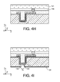
- Thinning can be achieved so that the distance d (measured in a direction parallel to the vector j orthogonal reference [O; i ; j ; k ] given on the Figure 4H ) separating the bottom of the first hole 104 and the rear face of the substrate 100 is less than 20 microns or less than or equal to 10 microns.
- the rear face of the substrate 100 may then be covered with an insulating layer 131 which may for example be based on SiO 2 and produced by deposition or by oxidation.
- a second hole 134 is then formed in a portion of the thickness of the facing substrate 100 and the first hole 104.
- This second hole 134 may be made to open onto the insulating layer 105 lining the bottom of the first hole 104.
- second hole 134 can be made for example by etching with KOH ( figure 4I ).
- the second hole 134 has a height H 2 and a smaller cross section than the first hole 104.
- the second hole 134 may be provided with a depth H 2 (measured in a direction parallel to the vector j orthogonal reference [O; i ; j ; k ]) less than 20 ⁇ m or preferably less than or equal to 10 ⁇ m.
- the second hole 134 is thus made with a height H 2 smaller than those of the first hole 104, and with a diameter or a critical dimension D 2 (the critical dimension or the diameter being measured in a direction parallel to the plane [ O; i ; k ] of the orthogonal reference [O; i ; j ; k ] on the figure 4I )
- a diameter or a critical dimension D 2 the critical dimension or the diameter being measured in a direction parallel to the plane [ O; i ; k ] of the orthogonal reference [O; i ; j ; k ] on the figure 4I
- D 2 the critical dimension or the diameter being measured in a direction parallel to the plane [ O; i ; k
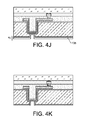
- the insulating layer 135 may be based on polymer such as for example BCB. This other insulating layer 135 may have a thickness e 2 for example between 10 nm and 10 microns.
- the insulating layer 135 is removed from the bottom of the second hole 134 as well as from the portion of the insulating layer 105 lining the bottom of the first hole 104. This removal may be carried out for example by means of an etching dry type RIE ("Reactive Ion Etching") for example based on CHF 3 -O 2 .
- RIE Reactive Ion Etching
- Another metal "growth” layer 137 can then be formed on the rear face of the substrate 100 so as to cover the insulating layer 131 as well as to cover the walls of the second hole 134.
- This other growth layer 137 can also be made at the bottom of the second hole 134.
- the growth layer 137 may be formed of a bi-layer, for example based on Ti and Cu or on TiN and Cu ( figure 4L ).
- a layer of metallic material 139 is formed so as to partially fill the second hole 134 and to cover the bottom and the walls of the latter, and possibly cover areas of the rear face of the substrate 100 located near the mouth of second hole 134.
- the partial filling of the second hole 134 is thus performed so that an area located in the center of the second hole 134 is not filled with metallic material ( figure 4M ).
- the metallic filling material 139 may for example be Cu. This produces the lower portion 142 of the vertical connection element.
- the central zone of the second hole 134 is also filled so as to fill the latter with a material 141 whose thermal expansion coefficient is less than that of the material or metallic materials lining the walls of the second hole 134.
- the material 141 may be insulating in order to produce a passivation layer on the rear face of the substrate 100.
- the insulating material 141 may be, for example, a polymeric material such as BCB.
- the thickness of the passivation layer may for example be between 0.5 ⁇ m and 20 ⁇ m.
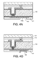
- An opening 143 is then made in the passivation layer 141 revealing an area 142b of the lower portion 142 of the vertical connection element resting on the rear face of the substrate 100 ( figure 4N ).
- a metal connection pad 146 is formed, for example based on Cu or formed of a stack of metal layers covered with a layer of Cu ( figure 4O ).
- the handle layer 121 is then removed, for example by performing shear shrinkage ( figure 4P ).
- a layer 231 which may be based on a material having a high coefficient of thermal expansion (CTE), for example greater than 20 ppm / ° C., and a Young's modulus high and for example greater than 150 GPa.
- CTE coefficient of thermal expansion
- the layer 231 may be chosen based on a material having a coefficient of thermal expansion and a Young's modulus greater than that of the material of the substrate 100 on which this layer 231 is deposited.
- the layer 231 may be, for example, based on AlN or TiW, particularly when the substrate is Si.
- the layer 231 may also have a thickness of, for example, between 1 ⁇ m and 20 ⁇ m, preferably of the order of 2 ⁇ m or 3 ⁇ m.
- the second hole 134 is then formed in a portion of the thickness of the facing substrate 100 and the first hole 104.
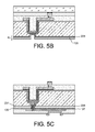
- This second hole 134 may be made in such a way as to open onto the insulating layer 105 lining the bottom of the first hole 104 ( Figure 5A ).
- Steps similar to those previously described in connection with the Figures 4K to 4M comprising removing the insulating layer 135 from the bottom of the second hole 134 and the insulating layer 105 at the bottom of the first hole 104 so as to expose the metal layer 107 at the bottom of the first hole 104, and then forming the layer of metallic material 139, the insulating material 141, and the connection pad 146.
Abstract
Description
L'invention concerne le domaine de la microélectronique et/ou nanoélectronique et des microsystèmes et/ou nano-systèmes, et en particulier celui des structures d'interconnexions verticales communément appelées vias TSV (TSV pour « Through Silicon Via ») traversant un substrat semi-conducteur.The invention relates to the field of microelectronics and / or nanoelectronics and microsystems and / or nano-systems, and in particular that of vertical interconnection structures commonly called TSV vias (TSV for "Through Silicon Via") traversing a semi substrate. -driver.
Elle prévoit la mise en oeuvre d'un dispositif microélectronique et/ou nanoélectronique doté d'une structure d'interconnexion verticale TSV de forme et d'agencement améliorés permettant de limiter les contraintes induites par les matériaux formant cette structure sur le reste du dispositif.It provides for the implementation of a microelectronic and / or nanoelectronic device with a vertical interconnection structure TSV of improved shape and arrangement to limit the stresses induced by the materials forming this structure on the rest of the device.
Lors de la réalisation de dispositifs électroniques comprenant une pluralité de substrats ou de puces empilé(e)s, on peut mettre en oeuvre des vias de type TSV traversant l'épaisseur d'un ou plusieurs de ces substrats ou de ces puces.When producing electronic devices comprising a plurality of substrates or stacked chips, it is possible to implement vias of the TSV type crossing the thickness of one or more of these substrates or of these chips.
Les vias TSV permettent de réaliser une connexion entre un élément conducteur situé sur une face appelée « face avant » ou du côté de la face avant d'un substrat et un autre élément conducteur situé sur une autre face appelée « face arrière » ou du côté de la face arrière dudit substrat.The vias TSV make it possible to make a connection between a conductive element situated on a face called "front face" or the side of the front face of a substrate and another conductive element located on another face called "back face" or on the side of the rear face of said substrate.
Plusieurs familles de procédés de réalisation de via TSV existent suivant que les via sont réalisés avant ou après ou en même temps que des composants électroniques à interconnecter.Several families of methods for producing via TSV exist depending on whether the via are made before or after or at the same time as electronic components to be interconnected.
Dans un procédé de type communément appelé « via first », les vias TSV sont réalisés avant les composants électroniques sur le substrat, notamment avant les transistors.In a method of the type commonly called " via first ", the vias TSV are made before the electronic components on the substrate, in particular before the transistors.
Dans un procédé de type communément appelé « via middle », les vias TSV sont réalisés après la réalisation des composants, mais avant les connexions électriques de ces derniers.In a method of the type commonly called " via middle ", the vias TSV are made after the completion of the components, but before the electrical connections of the latter.
Dans un procédé de type communément appelé « via last », les vias TSV sont réalisés après la fabrication des composants électroniques et de leurs connexions vers un dispositif extérieur.In a method of the type commonly called " via last ", vias TSV are made after the manufacture of the electronic components and their connections to an external device.
Les vias TSV sont formés par remplissage à l'aide d'un matériau conducteur d'au moins un trou traversant un support semi-conducteur. Le matériau métallique qui remplit le trou a généralement un coefficient de dilation thermique très différent de celui du support semi-conducteur.The vias TSV are formed by filling with a conductive material of at least one hole through a semiconductor medium. The metal material that fills the hole generally has a coefficient of thermal expansion very different from that of the semiconductor medium.
Lorsque le matériau de remplissage est du Cu, le coefficient de dilatation thermique peut être par exemple de l'ordre de 18 ppm/°C tandis que le coefficient de dilatation thermique d'un support à base de Si peut être de l'ordre par exemple de 2,6 ppm/°C.When the filling material is Cu, the coefficient of thermal expansion can be, for example, of the order of 18 ppm / ° C. whereas the coefficient of thermal expansion of a Si-based support can be of the order of example of 2.6 ppm / ° C.
En outre, dans le cas où les vias sont remplis ultérieurement au moyen d'un polymère de passivation permettant d'isoler le matériau métallique de celui du support, cet effet de dilation est également amplifié dans la mesure où les polymères de remplissage présentent des coefficients de dilatation encore plus élevés et compris par exemple entre 60 et 180 ppm/°C.In addition, in the case where the vias are subsequently filled by means of a passivation polymer for isolating the metallic material from that of the support, this expansion effect is also amplified insofar as the filling polymers have coefficients even higher expansion and for example between 60 and 180 ppm / ° C.
Une importante différence de coefficients de dilation thermique peut entrainer d'importantes contraintes mécaniques au sein d'un dispositif microélectronique, ces contraintes pouvant entrainer notamment un délaminage ou délamination du matériau métallique ou une rupture de zones de reprises de contact réalisées en face avant et en face arrière d'un substrat. L'ordre de grandeur typique de contraintes à ne pas dépasser est généralement de l'ordre de 100MPa pour, une contrainte supérieure à 500 Mpa pouvant aboutir à une rupture.A significant difference in thermal expansion coefficients can lead to significant mechanical stresses within a microelectronic device, these constraints possibly resulting in delamination or delamination of the metallic material or a rupture of contact recovery zones formed on the front face and in back side of a substrate. The typical order of magnitude of constraints not to be exceeded is generally of the order of 100 MPa for a stress greater than 500 MPa may lead to a rupture.
Le document: "
Dans ce procédé, le trou du via est réalisé à travers la face arrière du substrat et de manière à déboucher directement sur une zone métallique à connecter sans qu'une reprise de contact sur la face avant du substrat ne soit réalisée.In this method, the through hole is made through the rear face of the substrate and so as to lead directly to a metal zone to be connected without a contact recovery on the front face of the substrate is made.
Le document
Cette structure est formée d'un élément de connexion métallique tapissant les parois d'un trou traversant le substrat. Lors de l'étape de gravure du substrat, sa face avant est protégée par l'intermédiaire d'une couche de protection de projections engendrées par la gravure. Cette couche de protection peut être éventuellement conductrice et permettre en outre de réaliser une reprise de contact sur la face avant.This structure is formed of a metallic connection element lining the walls of a hole passing through the substrate. During the step of etching the substrate, its front face is protected by means of a protective layer of projections generated by the etching. This protective layer may be possibly conductive and also allow a resumption of contact on the front face.
Le document : "
Le document
Dans le procédé décrit dans ce document, la reprise de contact sur la face avant nécessite de réaliser de nombreuses étapes.In the method described in this document, the contact recovery on the front face requires many steps.
Les documents
Il se pose le problème de trouver une nouvelle structure de via TSV dans laquelle les phénomènes de contraintes seraient réduits, ainsi qu'un nouveau procédé de réalisation d'une telle structure.There is the problem of finding a new structure of via TSV in which the phenomena of constraints would be reduced, as well as a new method of producing such a structure.
La présente invention concerne tout d'abord un procédé de réalisation d'une structure d'interconnexion comprenant des étapes de :
- formation d'un premier trou à travers une première face d'un support sur laquelle un ou plusieurs composants électroniques sont réalisés ou destinés à être réalisés, le premier trou traversant partiellement le support et ayant une dimension critique D1 et une hauteur H1,
- réalisation d'une partie supérieure d'un élément de connexion conducteur par formation de matériau conducteur dans ledit premier trou de manière à recouvrir les parois et le fond dudit premier trou, une zone centrale du premier trou n'étant pas remplie par ledit matériau métallique,
- formation d'au moins un deuxième trou à travers une deuxième face du support opposée à ladite première face, ledit deuxième trou étant réalisé dans le prolongement du premier trou et débouchant sur ladite partie supérieure dudit élément de connexion, ledit deuxième trou étant également réalisé de manière à avoir une dimension critique D2 < D1 et une hauteur H2 < H1,
- réalisation d'une partie inférieure dudit élément de connexion conducteur par formation de matériau conducteur dans ledit deuxième trou de manière à recouvrir les parois et le fond du deuxième trou, une zone centrale dudit deuxième trou, n'étant pas remplie par ledit matériau conducteur.
- forming a first hole through a first face of a support on which one or more electronic components are made or intended to be made, the first hole partially passing through the support and having a critical dimension D 1 and a height H 1 ,
- providing an upper portion of a conductive connection member by forming conductive material in said first hole so as to cover the walls and the bottom of said first hole, a central zone of the first hole not being filled with said metallic material ,
- forming at least one second hole through a second face of the support opposite to said first face, said second hole being made in the extension of the first hole and opening on said upper portion of said connecting element, said second hole being also made of to have a critical dimension D 2 <D 1 and a height H 2 <H 1 ,
- providing a lower portion of said conductive connection member by forming conductive material in said second hole so as to cover the walls and bottom of the second hole, a central zone of said second hole not being filled with said conductive material.
Après la réalisation de la partie supérieure et préalablement à la formation dudit ou desdits deuxième(s) trou(s), le procédé comprend en outre la formation d'une couche d'un matériau donné sur ladite deuxième face du support, prévue de sorte que ledit matériau donné a un module d'Young et un coefficient de dilatation thermique supérieurs, respectivement, au module d'Young et au coefficient de dilatation thermique du support.After the completion of the upper part and prior to the formation of said second hole (s), the method further comprises the formation of a layer of a given material on said second face of the support, provided so said given material has a Young's modulus and a coefficient of thermal expansion greater, respectively, than the Young's modulus and the coefficient of thermal expansion of the support.
Un tel procédé permet la réalisation d'un via dans lequel les contraintes sont limitées.Such a method allows the realization of a via in which the constraints are limited.
Ladite couche de matériau donné permet de limiter les contraintes, et de jouer le rôle de couche d'absorption de contraintes en formant avec le support un bilame mécanique. Ce bilame permet de compenser les contraintes générées par la formation de matériau conducteur dans le premier trou et dans le deuxième trou.Said layer of given material makes it possible to limit the stresses, and to play the role of stress absorption layer by forming with the support a bimetallic bimetallic strip. This bimetal makes it possible to compensate for the stresses generated by the formation of conductive material in the first hole and in the second hole.
Selon une possibilité de mise en oeuvre du procédé, la dimension critique D1, la dimension critique D2, la hauteur H2, peuvent être prévues de sorte que (D1-D2)/H2 > 4.According to one possibility of implementing the method, the critical dimension D 1 , the critical dimension D 2 , the height H 2 can be provided so that (D 1 -D 2 ) / H 2> 4.
Selon une possibilité de mise en oeuvre du procédé, préalablement à la formation de ladite partie supérieure dudit élément de connexion, on peut former un matériau isolant de manière à tapisser le fond et les parois dudit premier trou. La formation dudit deuxième trou peut comprendre alors une gravure du support jusqu'au dit matériau isolant, le procédé comprenant en outre, préalablement à la formation de ladite partie inférieure dudit élément de connexion :
- la formation d'un matériau isolant de manière à tapisser les parois et le fond dudit deuxième trou,
- la gravure au fond du deuxième trou desdits matériaux isolants, de manière à prolonger ledit deuxième trou et dévoiler ladite partie supérieure dudit élément de connexion.
- forming an insulating material so as to line the walls and the bottom of said second hole,
- etching at the bottom of the second hole of said insulating materials, so as to extend said second hole and expose said upper portion of said connecting member.
Après la formation de ladite partie supérieure dudit élément de connexion conducteur et préalablement à la formation dudit ou desdits deuxième trou(s), une étape consistant à amincir le support du côté de ladite deuxième face du support peut être prévue.After forming said upper portion of said conductive connection member and prior to forming said second hole (s), a step of thinning the support on the side of said second side of the support may be provided.
Selon une possibilité de mise en oeuvre du procédé, le deuxième trou peut avoir une hauteur H2 telle que H2 < H1/10.According to one possible implementation of the method, the second hole may have a height H 2 as H 2 <H 1/10.
Selon une possibilité de mise en oeuvre du procédé, le deuxième trou peut avoir un diamètre D2 tel que D2 ≤ 0.5*D1.According to one possible implementation of the method, the second hole may have a diameter D 2 such that D 2 ≤ 0.5 * D 1 .
De tels rapports de forme permettent de limiter les contraintes au sein du via.Such form relationships make it possible to limit the constraints within the via.
Selon une possibilité de mise en oeuvre du procédé, après réalisation de ladite partie supérieure dudit élément de connexion conducteur, ladite zone centrale dudit premier trou peut être remplie d'un matériau isolant.According to a possibility of implementing the method, after making said upper part of said conductive connection element, said central zone of said first hole may be filled with an insulating material.
Afin de réduire les contraintes au sein du via, ledit matériau isolant de remplissage de ladite zone centrale du premier trou peut être prévu avec un coefficient de dilatation thermique plus faible que celui dudit matériau conducteur recouvrant les parois et le fond du premier trou.In order to reduce the stresses within the via, said insulating filler material of said central zone of the first hole may be provided with a lower coefficient of thermal expansion than that of said conductive material covering the walls and the bottom of the first hole.
Selon une possibilité de mise en oeuvre du procédé, après réalisation de ladite partie inférieure dudit élément de connexion conducteur ladite zone centrale dudit deuxième trou peut être remplie d'un matériau isolant.According to one possibility of implementing the method, after making said lower part of said conductive connection element, said central zone of said second hole may be filled with an insulating material.
Afin de réduire les contraintes au sein du via, ledit matériau isolant de remplissage de ladite zone centrale du deuxième trou peut avoir un coefficient de dilatation thermique plus faible que celui dudit matériau conducteur recouvrant les parois et le fond du deuxième trou.In order to reduce the stresses within the via, said insulating filler material of said central zone of the second hole may have a lower coefficient of thermal expansion than that of said conductive material covering the walls and the bottom of the second hole.
Selon une possibilité de mise en oeuvre du procédé, la réalisation de ladite partie supérieure dudit élément de connexion conducteur peut comprendre la formation d'une zone conductrice s'étendant sur, ou parallèlement à, la première face du support.According to one possible implementation of the method, the embodiment of said upper portion of said conductive connection element may comprise the formation of a conductive zone extending on or parallel to the first face of the support.
Après la réalisation de ladite partie inférieure dudit élément de connexion conducteur, le procédé peut comprendre la formation d'une zone dudit matériau conducteur s'étendant sur, ou parallèlement à, la deuxième face du support.After completion of said lower portion of said conductive connection member, the method may include forming an area of said conductive material extending on or parallel to the second face of the support.
La présente invention concerne également une structure d'interconnexion comprenant : un élément de connexion conducteur doté :
- d'une partie supérieure débouchant sur une première face d'un support sur laquelle un ou plusieurs composants électroniques sont réalisés ou destinés à être réalisés, la partie supérieure étant réalisé dans un premier trou traversant partiellement ledit support et ayant une dimension critique D1 et une hauteur H1, ladite partie supérieure étant formée de matériau conducteur recouvrant les parois et le fond d'un premier trou, une zone centrale du premier trou n'étant pas remplie par ledit matériau conducteur,
- d'une partie inférieure connectée à ladite partie supérieure et débouchant sur une deuxième face du support opposée à la première face, la partie inférieure étant réalisée dans un ou plusieurs deuxième(s) trou(s) communicant avec le premier trou et traversant partiellement ledit support, le ou les deuxièmes trou(s) ayant une dimension critique D2 < D1 et une hauteur H2 < H1, ladite partie inférieure étant formée de matériau conducteur recouvrant les parois et le fond du ou des deuxième trou(s), une zone centrale dudit ou desdits deuxième(s) trou(s) n'étant pas remplie par ledit matériau conducteur.
- an upper part opening on a first face of a support on which one or more electronic components are made or intended to be made, the upper part being made in a first hole partially passing through said support and having a critical dimension D 1 and a height H 1 , said upper part being formed of conductive material covering the walls and the bottom of a first hole, a central zone of the first hole not being filled with said conductive material,
- a lower part connected to said upper part and opening on a second face of the support opposite to the first face, the lower part being made in one or more second hole (s) communicating with the first hole and partially passing through said support, the second hole (s) having a critical dimension D 2 <D 1 and a height H 2 <H 1 , said lower portion being formed of conductive material covering the walls and the bottom of the second hole (s) a central zone of said second hole (s) not being filled by said conductive material.
Sur la deuxième face du support, une couche à base d'un matériau donné ayant un module d'Young et un coefficient de dilatation thermique supérieurs respectivement au module d'Young et au coefficient de dilatation thermique du support, est prévue.On the second face of the support, a layer based on a given material having a Young's modulus and a coefficient of thermal expansion greater than the Young's modulus and the coefficient of thermal expansion of the support, respectively, is provided.
Le matériau donné peut être par exemple de l'AlN ou du TiW, en particulier lorsque le matériau du support est du Si.The given material may be for example AlN or TiW, especially when the support material is Si.
Selon une possibilité de mise en oeuvre de la structure, la zone centrale dudit premier trou et/ou deuxième trou peut être remplie d'un matériau isolant.According to one possible implementation of the structure, the central zone of said first hole and / or second hole may be filled with an insulating material.
Selon une possibilité de mise en oeuvre de la structure, le matériau isolant remplissant la zone centrale dudit premier trou et/ou deuxième trou peut avoir un coefficient de dilatation thermique plus faible que celui dudit matériau conducteur.According to one possible implementation of the structure, the insulating material filling the central zone of said first hole and / or second hole may have a thermal expansion coefficient lower than that of said conductive material.
Selon une possibilité de mise en oeuvre de la structure, la dimension critique D1, la dimension critique D2, la hauteur H2, peuvent être prévues de sorte que (D1-D2)/H2 > 4.According to one possible implementation of the structure, the critical dimension D 1 , the critical dimension D 2 , the height H 2 can be provided so that (D 1 -D 2 ) / H 2> 4.
Selon une possibilité de mise en oeuvre de la structure, ledit ou lesdits deuxième(s) trou(s) peut ou peuvent avoir une hauteur H2 telle que H2 < H1/10.According to one possible implementation of the structure, said one or more second (s) hole (s) may or may have a height H 2 as H 2 <H 1/10.
Selon une possibilité de mise en oeuvre de la structure, ledit ou lesdits deuxième(s) trou(s) peut ou peuvent avoir un diamètre D2 tel que D2 ≤ 0.5*D1 According to one possible implementation of the structure, said second hole (s) may or may have a diameter D 2 such that D 2 ≤ 0.5 * D 1
Selon une possibilité de mise en oeuvre de la structure, dans laquelle ladite partie supérieure dudit élément de connexion métallique comprend une zone conductrice s'étendant sur ou parallèlement à la première face du support, ladite partie inférieure dudit élément de connexion conducteur peut comprendre une zone conductrice s'étendant sur ou parallèlement à la deuxième face du substrat.According to one possible implementation of the structure, wherein said upper part of said metallic connection element comprises a conductive zone extending on or parallel to the first face of the support, said part The bottom of said conductive connection element may comprise a conductive zone extending on or parallel to the second face of the substrate.
La présente invention sera mieux comprise à la lecture de la description d'exemples de réalisation donnés, à titre purement indicatif et nullement limitatif, en faisant référence aux dessins annexés sur lesquels :
- la
figure 1 illustre un exemple de structure d'interconnexion suivant l'invention, cette structure comprenant un élément de connexion traversant un support et étant configurée de manière à limiter les phénomènes de contraintes mécaniques induites par les matériaux la constituant, - les
figures 2A-2B illustrent des moyens pour libérer les contraintes mécaniques exercées au sein d'une structure d'interconnexion de type TSV mise en oeuvre suivant l'invention, - les
figures 3A-3H illustrent différents exemples de mise en oeuvre de la partie inférieure d'une structure d'interconnexion de type TSV suivant l'invention, - les
figures 4A-4P illustrent un exemple de procédé de réalisation suivant l'invention d'une structure d'interconnexion de type TSV, - les
figures 5A-5C illustrent un exemple de procédé de réalisation suivant l'invention d'une variante de structure d'interconnexion de type TSV mise en oeuvre suivant l'invention.
- the
figure 1 illustrates an example of an interconnection structure according to the invention, this structure comprising a connection element traversing a support and being configured so as to limit the phenomena of mechanical stresses induced by the materials constituting it, - the
Figures 2A-2B illustrate means for releasing the mechanical stresses exerted within a type of interconnection structure TSV implemented according to the invention, - the
Figures 3A-3H illustrate different examples of implementation of the lower part of a TSV type interconnection structure according to the invention, - the
Figures 4A-4P illustrate an exemplary embodiment method according to the invention of a type of interconnection structure TSV, - the
Figures 5A-5C illustrate an exemplary embodiment method according to the invention of a variant of the type of interconnection structure TSV implemented according to the invention.
Des parties identiques, similaires ou équivalentes des différentes figures portent les mêmes références numériques de façon à faciliter le passage d'une figure à l'autre.Identical, similar or equivalent parts of the different figures bear the same numerical references so as to facilitate the passage from one figure to another.
Les différentes parties représentées sur les figures ne le sont pas nécessairement selon une échelle uniforme, pour rendre les figures plus lisibles.The different parts shown in the figures are not necessarily in a uniform scale, to make the figures more readable.
Un exemple de structure d'interconnexion suivant l'invention va à présent être décrit en liaison avec la
Cette structure est de type TSV (TSV pour « Through silicon via ») et traverse un substrat 100 qui peut être semi-conducteur et, par exemple, à base de Si et avoir une épaisseur comprise, par exemple, entre 100 µm et 300 µm ou par exemple entre 10 µm et 100 µm.This structure is of the TSV type (TSV for "Through silicon via") and passes through a
Cette structure est formée d'un élément de connexion métallique 110 qui peut être, par exemple, à base de cuivre et comprend une partie supérieure 112 réalisée dans un premier trou 104 traversant partiellement le substrat 100 et débouchant du côté d'une face du substrat appelée « face avant ».This structure is formed of a
La face avant du substrat 100 est une face sur laquelle un ou plusieurs composants électroniques Ci tels que des transistors sont disposés (l'ensemble des composants Ci étant représenté de manière schématique par un cadre en trait discontinu sur la
La partie supérieure 112 de l'élément de connexion 110 est formée d'une zone métallique 112a tapissant le fond et les parois du premier trou 104 et d'au moins une autre zone métallique 112b s'étendant sur la face avant du substrat 100 ou parallèlement à la face avant du substrat 100 et qui peut jouer le rôle d'une zone de reprise de contact.The
Le premier trou 104 est également rempli en son centre d'une zone d'un matériau 111 dont le coefficient de dilatation thermique est inférieur à celui du matériau métallique de ladite partie supérieure 112 de l'élément de connexion 110. Ce matériau 111 peut être isolant et, par exemple, un polymère tel que du Benzocyclobutène (BCB).The
L'élément de connexion métallique 110 comprend également une partie inférieure 142 réalisée dans au moins un deuxième trou 134 communicant avec le premier trou 104 et débouchant du côté de la face du substrat appelée « face arrière », et qui est opposée à la face avant.The
La partie inférieure 142 de l'élément de connexion 110 est formée d'une zone métallique 142a tapissant le fond et les parois du deuxième trou 134 et d'au moins une autre zone métallique 142b s'étendant sur la face arrière du substrat 100 ou parallèlement à la face arrière du substrat 100. Cette autre zone métallique 142b peut jouer le rôle d'une zone de reprise de contact.The
Le deuxième trou 134 est également rempli en son centre d'un matériau 141 dont le coefficient de dilatation thermique est inférieur à celui du matériau métallique de ladite partie inférieure 142 de l'élément de connexion 110. Ce matériau 141 peut être isolant et par exemple à base d'un polymère tel que par exemple du Benzocyclobutène (BCB).The
Les parois du premier trou 104 et du deuxième trou 134 sont recouvertes respectivement d'épaisseur e1 et e2 de matériau diélectrique afin de permettre d'isoler électriquement l'élément de connexion 140 du substrat 100.The walls of the
Le premier trou 104 et le deuxième trou 134 peuvent être verticaux.The
Le premier trou 104 dans lequel la partie supérieure de l'élément de connexion est formée a une dimension critique D1 (mesurée dans une direction parallèle au plan [O;
Le deuxième trou 134 a une dimension critique D2 (mesurée dans une direction parallèle au plan [O;
Afin de permettre de limiter les contraintes au sein de la structure d'interconnexion, le premier trou 104 et le deuxième trou 134 sont prévus de sorte que H2 < H1 et que D2 < D1.In order to make it possible to limit the stresses within the interconnection structure, the
Le premier trou 104 peut être réalisé de sorte que sa hauteur H1 est au moins dix fois supérieure à celle H2 du deuxième trou 134. Le premier trou 104 peut être réalisé de sorte que sa section est supérieure à celle du deuxième trou 134, et en particulier de sorte que la dimension critique D1 du premier trou 104 est 4 supérieure à celle D2 du deuxième trou 134.The
Ainsi, de par la dimension des trous 104 et 134, des zones de substrat 100 autour de la partie inférieure 142 et sous la partie supérieure 112 de l'élément de connexion métallique 110, peuvent former des barreaux ou poutres 101 de rapport de forme, i.e. de longueur sur épaisseur, importante permettant un effet de ressort ou d'amortissement des contraintes au sein de la structure d'interconnexion.Thus, by the size of the
L'épaisseur ep des poutres 101 dépend notamment de la hauteur H2 de la partie inférieure 142 de l'élément de connexion et peut être de l'ordre de la différence entre H2 et l'épaisseur e1 de la couche isolante séparant l'élément de connexion 110 du substrat 100 au fond du premier trou 104.The thickness e p of the
La longueur Ip des poutres 101 sous la partie inférieure 142 de l'élément de connexion 140 dépend de la différence entre la dimension critique D1 du premier trou 104 et de la dimension critique D2 du deuxième trou 134. La longueur Ip peut être de l'ordre de la différence (D1 + e1) - (D2 + e2) entre la distance cumulée (D1 + e1) de la dimension critique D1 et de l'épaisseur e1 de la couche isolante séparant la partie supérieure 112 de l'élément 110 de connexion du substrat 100 au fond du premier trou 104, et la distance cumulée (D2 + e2) de la dimension critique D2 et l'épaisseur e2 de la couche isolante séparant la partie inférieure 142 de l'élément 110 de connexion du substrat 100 au niveau des parois du deuxième trou 134.The length I p of the
Dans un cas par exemple où e1 ≈ e2, pour permettre une limitation importante des contraintes, le rapport (D1-D2)/H2 peut être prévu par exemple d'au moins 4.In a case for example where e 1 ≈ e 2 , to allow a significant limitation of the constraints, the ratio (D 1 -D 2 ) / H 2 can be provided for example of at least 4.
L'agencement de l'élément de connexion sous forme de zones tapissant les parois du premier trou 104 et du deuxième trou 134 permet de conférer à la structure une bonne résistance mécanique et contribue également à une limitation des contraintes dans la structure d'interconnexion.The arrangement of the connection element in the form of zones lining the walls of the
Le premier trou 104 peut être également réalisé de sorte qu'il comporte un fond doté de bords arrondis 104a. Cela peut contribuer également à une réduction des contraintes dans la structure d'interconnexion.The
La face arrière du substrat 100 est recouverte d'une couche 231 qui est prévue à base d'un matériau présentant un coefficient de dilatation thermique (CTE) élevé, par exemple supérieur à 20 ppm/°C et un module d'Young élevé et par exemple supérieur à 150 GPa. La couche 231 est choisie à base d'un matériau ayant un coefficient de dilatation thermique et un module d'Young supérieurs à celle du matériau du substrat 100 sur lequel cette couche 231 est déposée. Le substrat 100 et la couche 231 forment un bilame mécanique permettant de réduire les contraintes générées par le matériau de l'élément de connexion 110.The rear face of the
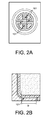
Sur les
La partie supérieure 112 de l'élément de connexion 110 est soutenue par des zones du substrat 100 formant des poutres 101 sous les bords arrondis du premier trou 104, ces poutres 101 ayant un rapport de forme prévu de manière à permettre de libérer les contraintes induites par le matériau métallique.The
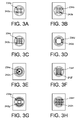
Sur les
Dans l'exemple des
Dans les exemples des
Selon d'autres exemples illustrés sur les
Selon un autre exemple de réalisation illustré sur la
Selon un autre exemple de réalisation illustré sur la
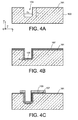
Un exemple de procédé de réalisation d'une structure d'interconnexion TSV suivant l'invention, va à présent être donné en liaison avec les
Dans cet exemple, le matériau de départ peut être un substrat 100 semi-conducteur, par exemple à base de Si et d'épaisseur par exemple comprise entre 100 µm et 300 µm, recouvert sur une de ses faces appelée « face avant » d'une couche isolante 101 qui peut être par exemple à base de SiO2 et d'épaisseur par exemple de l'ordre de 500 nm.In this example, the starting material may be a
Sur la face avant du substrat 100, un ou plusieurs composants électroniques tels que des transistors peuvent être déjà réalisés.On the front face of the
On forme tout d'abord un premier trou 104 dans une partie de l'épaisseur du substrat 100. Le premier trou 104 peut être vertical (la direction verticale étant une direction parallèle au vecteur
Par « dimension critique » d'un élément ou d'un motif ou d'une zone, on entend tout au long de la présente description la plus petite dimension de cet élément, ou de ce motif, ou de cette zone, hormis son épaisseur ou sa hauteur ou sa profondeur (mesurée dans une direction parallèle au vecteur
On peut ensuite former sur les parois et le fond du premier trou 104 une deuxième couche isolante 105 dans la continuité de la première couche isolante 101.It is then possible to form on the walls and the bottom of the
Cela peut être réalisé par exemple par oxydation thermique du matériau semi-conducteur du substrat 100 ou par dépôt, par exemple par dépôt de type SACVD (« Sub-Atmospheric Pressure Chemical Vapor Deposition ») ou par dépôt LPCVD (« Low Pressure Chemical Vapor Deposition). La deuxième couche isolante 105 peut être prévue, par exemple, avec une épaisseur e1 sensiblement égale à celle de la couche isolante 101 recouvrant la face avant du substrat 100 et par exemple comprise entre 10 nm et 10 µm.This can be achieved, for example, by thermal oxidation of the semiconductor material of the
Puis (
Selon une autre possibilité, le bi-couches peut être formé par exemple à base de TiN et de Cu et être déposé par exemple par CVD (« Chemical Vapor Deposition »). La couche de croissance 107 est prévue pour favoriser la croissance d'un matériau métallique tel que par exemple du Cu sur les parois et au fond du trou 104.According to another possibility, the bi-layer may be formed for example based on TiN and Cu and be deposited for example by CVD ("Chemical Vapor Deposition"). The
Ainsi, on forme ensuite une couche de matériau métallique 109 de manière effectuer un remplissage partiel du premier trou 104. Ce remplissage est réalisé de manière à tapisser le fond et les parois du premier trou 104, et peut être réalisé de manière à recouvrir des zones de la face avant du substrat 100 situées à proximité de l'embouchure du premier trou 104. Le remplissage partiel du premier trou 104 est effectué de sorte qu'une zone située au centre du premier trou 104 n'est pas remplie de matériau métallique. Le matériau métallique peut être par exemple du Cu et peut être formé par un procédé ECD, (ECD pour « Electrochemical Deposition »). L'épaisseur de la couche de matériau métallique 109 réalisée peut être par exemple de l'ordre de 10 µm.Thus, a layer of
On forme ainsi une partie supérieure 112 d'un élément de connexion 110 vertical ou via dans le premier trou 104.Thus, an
Ensuite, on effectue un retrait de la couche de croissance 107 dans des zones situées sur la face avant du substrat 100 et autour de la partie supérieure 112 de l'élément de connexion 110 vertical. Cela peut être réalisé en effectuant par exemple une gravure chimique humide à l'aide de H2SO4 ou de HF (
Puis, on forme une couche 111 à base d'un matériau ayant un coefficient de dilatation thermique inférieur à celui des matériaux 107 et 109, de manière à remplir la zone centrale du trou 104 et recouvrir la face avant du substrat 100. Cette couche 111 peut être isolante. Cette couche isolante 111 peut être, par exemple, à base de polymère et réalisée de manière à recouvrir la couche métallique 109 et remplir le trou 104. Le matériau polymère de la couche isolante 111 peut être par exemple du Benzocylcobutène (BCB). L'épaisseur isolante 111 peut être par exemple comprise entre 10 µm et 30 µm (
On réalise ensuite une ouverture 113 dans la couche isolante 111 dévoilant une zone de la couche métallique 109 reposant sur la face avant du substrat 100 (
Puis, on forme dans cette ouverture 113 un plot de connexion métallique 116 par exemple à base de Cu ou formé d'un empilement de couches métalliques recouvert d'une couche de Cu. Le plot de connexion 116 peut avoir une hauteur (mesurée dans une direction parallèle au vecteur
Ensuite, on forme une couche poignée 121 sur la face avant du substrat 100. Cette couche poignée 121 peut être par exemple à base de verre ou de silicium et assemblée au substrat 100 par l'intermédiaire d'une couche 119 de collage par exemple à base d'un polymère, qui peut être un matériau thermoplastique ayant des propriétés adhésives. La couche 119 de collage peut avoir une épaisseur comprise par exemple entre 100 µm et 1000 µm (
On peut ensuite réaliser un amincissement du substrat 100, par retrait d'une portion du substrat 100 située du côté de la face appelée « face arrière » et qui est opposée à la face avant.It is then possible to thin the
On diminue ainsi la distance d entre le fond du premier trou 104 et la face arrière du substrat 100. L'épaisseur du substrat 100 que l'on retire peut être par exemple comprise entre 100 µm et 1000 µm.This decreases the distance d between the bottom of the
L'amincissement peut être réalisé de sorte que la distance d (mesurée dans une direction parallèle au vecteur
La face arrière du substrat 100 peut être ensuite recouverte d'une couche isolante 131 qui peut être par exemple à base de SiO2 et réalisée par dépôt ou par oxydation.The rear face of the
On forme ensuite un deuxième trou 134 dans une partie de l'épaisseur du substrat 100 en regard et du premier trou 104. Ce deuxième trou 134 peut être réalisé de manière à déboucher sur la couche isolante 105 tapissant le fond du premier trou 104. Le deuxième trou 134 peut être réalisé par exemple par gravure à l'aide de KOH (
Le deuxième trou 134 a une hauteur H2 et une section transversale plus faible que celle du premier trou 104.The
Le deuxième trou 134 peut être prévu avec une profondeur H2 (mesurée dans une direction parallèle au vecteur
On peut ensuite former sur les parois et le fond du deuxième trou 134 une autre couche isolante 135 dans la continuité de la couche isolante 131. Cela peut être réalisé par exemple par oxydation thermique du matériau semi-conducteur du substrat 100, en particulier lorsque la couche isolante 135 est à base de SiO2. Selon une autre possibilité (
Puis, on effectue un retrait de la couche isolante 135 au fond du deuxième trou 134 ainsi que de la portion de la couche isolante 105 tapissant le fond du premier trou 104. Ce retrait peut être effectué par exemple à l'aide d'une gravure sèche de type RIE («Reactive Ion Etching ») par exemple à base de CHF3-O2. On dévoile ainsi une zone métallique de la partie supérieure 112 de l'élément de connexion métallique (
On peut ensuite former une autre couche 137 « de croissance » métallique sur la face arrière du substrat 100 de manière à recouvrir la couche isolante 131 ainsi qu'à tapisser les parois du deuxième trou 134. Cette autre couche de croissance 137 peut être également réalisée au fond du deuxième trou 134. La couche de croissance 137 peut être formée d'un bi-couches par exemple à base de Ti et de Cu ou à base de TiN et de Cu (
Ensuite, on forme une couche de matériau métallique 139 de manière effectuer un remplissage partiel du deuxième trou 134 et à tapisser le fond et les parois de ce dernier, et éventuellement recouvrir des zones de la face arrière du substrat 100 situées à proximité de l'embouchure du deuxième trou 134.Next, a layer of
Le remplissage partiel du deuxième trou 134 est ainsi effectué de sorte qu'une zone située au centre du deuxième trou 134 n'est pas remplie de matériau métallique (
Puis, la zone centrale du deuxième trou 134 est également remplie de manière à combler ce dernier avec un matériau 141 dont le coefficient de dilatation thermique est inférieur à celui du matériau ou des matériaux métalliques tapissant les parois du deuxième trou 134. Le matériau 141 peut être isolant afin de réaliser une couche de passivation sur la face arrière du substrat 100. Le matériau 141 isolant peut être, par exemple, un matériau polymère tel que du BCB. L'épaisseur de la couche de passivation peut être par exemple comprise entre 0.5 µm et 20 µm.Then, the central zone of the
On réalise ensuite une ouverture 143 dans la couche de passivation 141 dévoilant une zone 142b de la partie inférieure 142 de l'élément de connexion vertical reposant sur la face arrière du substrat 100 (
Puis, on forme dans cette ouverture 143, un plot de connexion métallique 146 par exemple à base de Cu ou formé d'un empilement de couches métalliques recouvert d'une couche de Cu (
On retire ensuite la couche poignée 121, par exemple en effectuant un retrait par cisaillement (
Une variante du procédé de réalisation d'une structure d'interconnexion tel que décrit précédemment en liaison avec les
Après l'étape d'amincissement décrite en liaison avec la
La couche 231 peut être en particulier choisie à base d'un matériau ayant un coefficient de dilatation thermique et un module d'Young supérieurs à celle du matériau du substrat 100 sur lequel cette couche 231 est déposée.In particular, the
La couche 231 peut être, par exemple, à base d'AlN, ou de TiW, en particulier lorsque le substrat est en Si.The
La couche 231 peut également avoir une épaisseur comprise, par exemple, entre 1 µm et 20 µm, de préférence de l'ordre de 2 µm ou 3 µm.The
On forme ensuite le deuxième trou 134 dans une partie de l'épaisseur du substrat 100 en regard et du premier trou 104. Ce deuxième trou 134 peut être réalisé de manière à déboucher sur la couche isolante 105 tapissant le fond du premier trou 104 (
On peut ensuite former sur les parois et le fond du deuxième trou 134 une couche isolante 135, par exemple à base de polymère tel que par exemple du BCB (
On réalise ensuite des étapes semblables à celles décrites précédemment en liaison avec les
Claims (19)
le procédé comprenant en outre, préalablement à la formation de ladite partie inférieure (142) dudit élément de connexion :
the method further comprising, prior to forming said lower portion (142) of said connecting member:
Applications Claiming Priority (1)
| Application Number | Priority Date | Filing Date | Title |
|---|---|---|---|
| FR1162372A FR2985088B1 (en) | 2011-12-23 | 2011-12-23 | VIA TSV WITH STRESS RELEASE STRUCTURE AND METHOD FOR MANUFACTURING THE SAME |
Publications (3)
| Publication Number | Publication Date |
|---|---|
| EP2608253A2 true EP2608253A2 (en) | 2013-06-26 |
| EP2608253A3 EP2608253A3 (en) | 2014-02-19 |
| EP2608253B1 EP2608253B1 (en) | 2016-07-13 |
Family
ID=47325980
Family Applications (1)
| Application Number | Title | Priority Date | Filing Date |
|---|---|---|---|
| EP12197423.2A Active EP2608253B1 (en) | 2011-12-23 | 2012-12-17 | TSV provided with a stress-release structure and method for manufacturing same |
Country Status (3)
| Country | Link |
|---|---|
| US (1) | US9536837B2 (en) |
| EP (1) | EP2608253B1 (en) |
| FR (1) | FR2985088B1 (en) |
Cited By (1)
| Publication number | Priority date | Publication date | Assignee | Title |
|---|---|---|---|---|
| CN107240579A (en) * | 2017-05-23 | 2017-10-10 | 华进半导体封装先导技术研发中心有限公司 | The RDL methods in package shape of pinboard |
Families Citing this family (6)
| Publication number | Priority date | Publication date | Assignee | Title |
|---|---|---|---|---|
| FR3012237B1 (en) | 2013-10-22 | 2017-03-03 | Commissariat Energie Atomique | ELECTRONIC CHIP COMPRISING PROTECTIVE MEANS ON ITS REAR PANEL |
| US9147642B2 (en) * | 2013-10-31 | 2015-09-29 | Nanya Technology Corporation | Integrated circuit device |
| FR3032556B1 (en) | 2015-02-11 | 2017-03-17 | Commissariat Energie Atomique | RF TRANSMISSION DEVICE WITH INTEGRATED ELECTROMAGNETIC WAVE REFLECTOR |
| US11270955B2 (en) * | 2018-11-30 | 2022-03-08 | Texas Instruments Incorporated | Package substrate with CTE matching barrier ring around microvias |
| US11289370B2 (en) | 2020-03-02 | 2022-03-29 | Nanya Technology Corporation | Liner for through-silicon via |
| CN111799177B (en) * | 2020-07-14 | 2023-09-29 | 通富微电科技(南通)有限公司 | Method for manufacturing semiconductor device |
Citations (5)
| Publication number | Priority date | Publication date | Assignee | Title |
|---|---|---|---|---|
| EP0363256B1 (en) | 1988-09-29 | 1992-04-22 | Commissariat A L'energie Atomique | Method of making electrical connections through a substrate |
| US5343071A (en) | 1993-04-28 | 1994-08-30 | Raytheon Company | Semiconductor structures having dual surface via holes |
| US20080076195A1 (en) | 2006-09-26 | 2008-03-27 | Hymite A/S | Formation of through-wafer electrical interconnections and other structures using a thin dielectric membrane |
| US20080081398A1 (en) | 2006-10-02 | 2008-04-03 | Fionix Inc. | Cap Wafer for Wafer Bonded Packaging and Method for Manufacturing the Same |
| US20100264548A1 (en) | 2009-04-16 | 2010-10-21 | Freescale Semiconductor, Inc. | Through substrate vias |
Family Cites Families (13)
| Publication number | Priority date | Publication date | Assignee | Title |
|---|---|---|---|---|
| US5910687A (en) * | 1997-01-24 | 1999-06-08 | Chipscale, Inc. | Wafer fabrication of die-bottom contacts for electronic devices |
| JP4248928B2 (en) * | 2003-05-13 | 2009-04-02 | ローム株式会社 | Semiconductor chip manufacturing method, semiconductor device manufacturing method, semiconductor chip, and semiconductor device |
| JP4265668B2 (en) * | 2007-03-08 | 2009-05-20 | ソニー株式会社 | Circuit board manufacturing method and circuit board |
| US20090045475A1 (en) * | 2007-08-14 | 2009-02-19 | Honeywell International Inc. | Double sided integrated processing and sensing chip |
| FR2923080A1 (en) * | 2007-10-26 | 2009-05-01 | St Microelectronics Rousset | Forming vias in semiconductor wafer, by making wafer having closed perimeter on its front side, filling wafer with dielectric material, thinning wafer by abrasion and/or etching, and removing semiconductor extending inside perimeter |
| US8017515B2 (en) * | 2008-12-10 | 2011-09-13 | Stats Chippac, Ltd. | Semiconductor device and method of forming compliant polymer layer between UBM and conformal dielectric layer/RDL for stress relief |
| TW201114003A (en) * | 2008-12-11 | 2011-04-16 | Xintec Inc | Chip package structure and method for fabricating the same |
| TWI471977B (en) * | 2009-05-15 | 2015-02-01 | Xintec Inc | Power mosfet package |
| JP5150566B2 (en) * | 2009-06-22 | 2013-02-20 | 株式会社東芝 | Semiconductor device and camera module |
| TWI579995B (en) * | 2009-08-19 | 2017-04-21 | Xintex Inc | Chip package and fabrication method thereof |
| US8368228B2 (en) * | 2009-10-19 | 2013-02-05 | Jeng-Jye Shau | Area efficient through-hole connections |
| TWI515930B (en) * | 2010-05-31 | 2016-01-01 | 精材科技股份有限公司 | Light-emitting diode submount, light-emitting diode package and fabrication method thereof |
| US9018094B2 (en) * | 2011-03-07 | 2015-04-28 | Invensas Corporation | Substrates with through vias with conductive features for connection to integrated circuit elements, and methods for forming through vias in substrates |
-
2011
- 2011-12-23 FR FR1162372A patent/FR2985088B1/en not_active Expired - Fee Related
-
2012
- 2012-12-17 EP EP12197423.2A patent/EP2608253B1/en active Active
- 2012-12-21 US US13/725,020 patent/US9536837B2/en active Active
Patent Citations (5)
| Publication number | Priority date | Publication date | Assignee | Title |
|---|---|---|---|---|
| EP0363256B1 (en) | 1988-09-29 | 1992-04-22 | Commissariat A L'energie Atomique | Method of making electrical connections through a substrate |
| US5343071A (en) | 1993-04-28 | 1994-08-30 | Raytheon Company | Semiconductor structures having dual surface via holes |
| US20080076195A1 (en) | 2006-09-26 | 2008-03-27 | Hymite A/S | Formation of through-wafer electrical interconnections and other structures using a thin dielectric membrane |
| US20080081398A1 (en) | 2006-10-02 | 2008-04-03 | Fionix Inc. | Cap Wafer for Wafer Bonded Packaging and Method for Manufacturing the Same |
| US20100264548A1 (en) | 2009-04-16 | 2010-10-21 | Freescale Semiconductor, Inc. | Through substrate vias |
Non-Patent Citations (2)
| Title |
|---|
| D. HENRY ET AL.: "Development and characterisation of high electrical performances TSV for 3D applications", EPTC CONFERENCE, 2009 |
| D. Y. CHEN ET AL.: "Enabling 3d-IC foundry technologies for 28 nm node and beyond: TSV integration with high throughput die-to-wafer stacking", TSMC |
Cited By (1)
| Publication number | Priority date | Publication date | Assignee | Title |
|---|---|---|---|---|
| CN107240579A (en) * | 2017-05-23 | 2017-10-10 | 华进半导体封装先导技术研发中心有限公司 | The RDL methods in package shape of pinboard |
Also Published As
| Publication number | Publication date |
|---|---|
| FR2985088A1 (en) | 2013-06-28 |
| US9536837B2 (en) | 2017-01-03 |
| US20130161828A1 (en) | 2013-06-27 |
| EP2608253A3 (en) | 2014-02-19 |
| FR2985088B1 (en) | 2015-04-17 |
| EP2608253B1 (en) | 2016-07-13 |
Similar Documents
| Publication | Publication Date | Title |
|---|---|---|
| EP2608253B1 (en) | TSV provided with a stress-release structure and method for manufacturing same | |
| EP2816624B1 (en) | Method for producing a through substrate via and a through substrate capacitor in a substrate | |
| EP2337067B1 (en) | Making TSV interconnection structures composed of an insulating contour and a conducting area located in the contour and separate from the contour | |
| FR2968130A1 (en) | SEMICONDUCTOR DEVICE COMPRISING CAPACITOR AND ELECTRICAL CONNECTION VIA AND METHOD FOR MANUFACTURING THE SAME | |
| WO2001009944A1 (en) | Method for producing via-connections in a substrate and substrate equipped with same | |
| FR2992467A1 (en) | METHOD FOR MAKING A COMPONENT WITH A THROUGH ELECTRIC CONTACT AND COMPONENT OBTAINED | |
| EP2154635B1 (en) | Apparatus for detection of attacks on a circuit chip | |
| EP2738796A2 (en) | Method for producing a flip-chip structure for assembling microelectronic devices comprising an insulating block for guiding a connecting element and corresponding device | |
| WO2021099713A1 (en) | Method for manufacturing a functional chip suitable for being assembled to wire elements | |
| EP2365741B1 (en) | Method for metallizing blind vias | |
| WO2007066037A1 (en) | Resistance in an integrated circuit | |
| EP2750185B1 (en) | Improved method for manufacturing a contact structure | |
| EP2791969B1 (en) | Forming a via electrical connection | |
| FR2901635A1 (en) | Front and rear surfaces three dimensional electrical connection forming method for e.g. silicon substrate, involves engraving lines and trenches, and realising metallization of walls of lines and base of trenches on surfaces by layers | |
| EP2862836B1 (en) | Method for electrochemically producing at least one porous region of a micro- and/or nanoelectronic structure | |
| EP2543625B1 (en) | Method for producing a metal insert in a timepiece | |
| EP3031775B1 (en) | Method for producing an electrical connection in a blind via | |
| EP2498287B1 (en) | Method for making vertical interconnections through structured layers | |
| FR3009649A1 (en) | INTERCONNECTING MULTIPLE LEVELS OF A STACK OF ELECTRONIC COMPONENT SUPPORTS | |
| FR2917231A1 (en) | Microelectronic device e.g. metal insulation metal condenser/capacitor, realization method, involves incorporating isolating blocks in metallic zones that forms lower reinforcement part of metal insulation metal condenser/capacitor | |
| EP3537489B1 (en) | Method for manufacturing a penetrating device | |
| FR2978296A1 (en) | ELECTRONIC CHIP COMPRISING CONNECTION PILLARS, AND METHOD OF MANUFACTURE | |
| FR2957191A1 (en) | Electrical interconnection support structure i.e. interposer, fabricating method for e.g. micro electromechanical system integrated circuits, involves depositing electric contact point on upper face at level of wire, and removing backplate | |
| EP2519087B1 (en) | Cover for encapsulating a system with electrical connections, manufacturing process therefore, encapsulated system comprising such a cover and piling of such systems | |
| FR3022697A1 (en) | ELECTRICAL CONNECTION DEVICE WITH CONNECTING ELEMENTS COMPRISING DEFORMABLE MEMBRANES |
Legal Events
| Date | Code | Title | Description |
|---|---|---|---|
| AK | Designated contracting states |
Kind code of ref document: A2 Designated state(s): AL AT BE BG CH CY CZ DE DK EE ES FI FR GB GR HR HU IE IS IT LI LT LU LV MC MK MT NL NO PL PT RO RS SE SI SK SM TR |
|
| AX | Request for extension of the european patent |
Extension state: BA ME |
|
| PUAI | Public reference made under article 153(3) epc to a published international application that has entered the european phase |
Free format text: ORIGINAL CODE: 0009012 |
|
| PUAL | Search report despatched |
Free format text: ORIGINAL CODE: 0009013 |
|
| AK | Designated contracting states |
Kind code of ref document: A3 Designated state(s): AL AT BE BG CH CY CZ DE DK EE ES FI FR GB GR HR HU IE IS IT LI LT LU LV MC MK MT NL NO PL PT RO RS SE SI SK SM TR |
|
| AX | Request for extension of the european patent |
Extension state: BA ME |
|
| RIC1 | Information provided on ipc code assigned before grant |
Ipc: H01L 21/768 20060101AFI20140110BHEP Ipc: H01L 23/48 20060101ALI20140110BHEP |
|
| 17P | Request for examination filed |
Effective date: 20140502 |
|
| RBV | Designated contracting states (corrected) |
Designated state(s): AL AT BE BG CH CY CZ DE DK EE ES FI FR GB GR HR HU IE IS IT LI LT LU LV MC MK MT NL NO PL PT RO RS SE SI SK SM TR |
|
| GRAP | Despatch of communication of intention to grant a patent |
Free format text: ORIGINAL CODE: EPIDOSNIGR1 |
|
| INTG | Intention to grant announced |
Effective date: 20160204 |
|
| GRAS | Grant fee paid |
Free format text: ORIGINAL CODE: EPIDOSNIGR3 |
|
| GRAA | (expected) grant |
Free format text: ORIGINAL CODE: 0009210 |
|
| AK | Designated contracting states |
Kind code of ref document: B1 Designated state(s): AL AT BE BG CH CY CZ DE DK EE ES FI FR GB GR HR HU IE IS IT LI LT LU LV MC MK MT NL NO PL PT RO RS SE SI SK SM TR |
|
| REG | Reference to a national code |
Ref country code: GB Ref legal event code: FG4D Free format text: NOT ENGLISH |
|
| REG | Reference to a national code |
Ref country code: AT Ref legal event code: REF Ref document number: 812927 Country of ref document: AT Kind code of ref document: T Effective date: 20160715 Ref country code: CH Ref legal event code: EP |
|
| REG | Reference to a national code |
Ref country code: IE Ref legal event code: FG4D Free format text: LANGUAGE OF EP DOCUMENT: FRENCH |
|
| REG | Reference to a national code |
Ref country code: DE Ref legal event code: R096 Ref document number: 602012020392 Country of ref document: DE |
|
| REG | Reference to a national code |
Ref country code: LT Ref legal event code: MG4D |
|
| REG | Reference to a national code |
Ref country code: NL Ref legal event code: MP Effective date: 20160713 |
|
| REG | Reference to a national code |
Ref country code: AT Ref legal event code: MK05 Ref document number: 812927 Country of ref document: AT Kind code of ref document: T Effective date: 20160713 |
|
| REG | Reference to a national code |
Ref country code: FR Ref legal event code: PLFP Year of fee payment: 5 |
|
| PG25 | Lapsed in a contracting state [announced via postgrant information from national office to epo] |
Ref country code: LT Free format text: LAPSE BECAUSE OF FAILURE TO SUBMIT A TRANSLATION OF THE DESCRIPTION OR TO PAY THE FEE WITHIN THE PRESCRIBED TIME-LIMIT Effective date: 20160713 Ref country code: NL Free format text: LAPSE BECAUSE OF FAILURE TO SUBMIT A TRANSLATION OF THE DESCRIPTION OR TO PAY THE FEE WITHIN THE PRESCRIBED TIME-LIMIT Effective date: 20160713 Ref country code: FI Free format text: LAPSE BECAUSE OF FAILURE TO SUBMIT A TRANSLATION OF THE DESCRIPTION OR TO PAY THE FEE WITHIN THE PRESCRIBED TIME-LIMIT Effective date: 20160713 Ref country code: RS Free format text: LAPSE BECAUSE OF FAILURE TO SUBMIT A TRANSLATION OF THE DESCRIPTION OR TO PAY THE FEE WITHIN THE PRESCRIBED TIME-LIMIT Effective date: 20160713 Ref country code: IS Free format text: LAPSE BECAUSE OF FAILURE TO SUBMIT A TRANSLATION OF THE DESCRIPTION OR TO PAY THE FEE WITHIN THE PRESCRIBED TIME-LIMIT Effective date: 20161113 Ref country code: HR Free format text: LAPSE BECAUSE OF FAILURE TO SUBMIT A TRANSLATION OF THE DESCRIPTION OR TO PAY THE FEE WITHIN THE PRESCRIBED TIME-LIMIT Effective date: 20160713 Ref country code: NO Free format text: LAPSE BECAUSE OF FAILURE TO SUBMIT A TRANSLATION OF THE DESCRIPTION OR TO PAY THE FEE WITHIN THE PRESCRIBED TIME-LIMIT Effective date: 20161013 Ref country code: IT Free format text: LAPSE BECAUSE OF FAILURE TO SUBMIT A TRANSLATION OF THE DESCRIPTION OR TO PAY THE FEE WITHIN THE PRESCRIBED TIME-LIMIT Effective date: 20160713 |
|
| PG25 | Lapsed in a contracting state [announced via postgrant information from national office to epo] |
Ref country code: ES Free format text: LAPSE BECAUSE OF FAILURE TO SUBMIT A TRANSLATION OF THE DESCRIPTION OR TO PAY THE FEE WITHIN THE PRESCRIBED TIME-LIMIT Effective date: 20160713 Ref country code: PL Free format text: LAPSE BECAUSE OF FAILURE TO SUBMIT A TRANSLATION OF THE DESCRIPTION OR TO PAY THE FEE WITHIN THE PRESCRIBED TIME-LIMIT Effective date: 20160713 Ref country code: AT Free format text: LAPSE BECAUSE OF FAILURE TO SUBMIT A TRANSLATION OF THE DESCRIPTION OR TO PAY THE FEE WITHIN THE PRESCRIBED TIME-LIMIT Effective date: 20160713 Ref country code: PT Free format text: LAPSE BECAUSE OF FAILURE TO SUBMIT A TRANSLATION OF THE DESCRIPTION OR TO PAY THE FEE WITHIN THE PRESCRIBED TIME-LIMIT Effective date: 20161114 Ref country code: SE Free format text: LAPSE BECAUSE OF FAILURE TO SUBMIT A TRANSLATION OF THE DESCRIPTION OR TO PAY THE FEE WITHIN THE PRESCRIBED TIME-LIMIT Effective date: 20160713 Ref country code: LV Free format text: LAPSE BECAUSE OF FAILURE TO SUBMIT A TRANSLATION OF THE DESCRIPTION OR TO PAY THE FEE WITHIN THE PRESCRIBED TIME-LIMIT Effective date: 20160713 Ref country code: GR Free format text: LAPSE BECAUSE OF FAILURE TO SUBMIT A TRANSLATION OF THE DESCRIPTION OR TO PAY THE FEE WITHIN THE PRESCRIBED TIME-LIMIT Effective date: 20161014 |
|
| REG | Reference to a national code |
Ref country code: DE Ref legal event code: R097 Ref document number: 602012020392 Country of ref document: DE |
|
| PG25 | Lapsed in a contracting state [announced via postgrant information from national office to epo] |
Ref country code: EE Free format text: LAPSE BECAUSE OF FAILURE TO SUBMIT A TRANSLATION OF THE DESCRIPTION OR TO PAY THE FEE WITHIN THE PRESCRIBED TIME-LIMIT Effective date: 20160713 Ref country code: RO Free format text: LAPSE BECAUSE OF FAILURE TO SUBMIT A TRANSLATION OF THE DESCRIPTION OR TO PAY THE FEE WITHIN THE PRESCRIBED TIME-LIMIT Effective date: 20160713 |
|
| PLBE | No opposition filed within time limit |
Free format text: ORIGINAL CODE: 0009261 |
|
| STAA | Information on the status of an ep patent application or granted ep patent |
Free format text: STATUS: NO OPPOSITION FILED WITHIN TIME LIMIT |
|
| PG25 | Lapsed in a contracting state [announced via postgrant information from national office to epo] |
Ref country code: DK Free format text: LAPSE BECAUSE OF FAILURE TO SUBMIT A TRANSLATION OF THE DESCRIPTION OR TO PAY THE FEE WITHIN THE PRESCRIBED TIME-LIMIT Effective date: 20160713 Ref country code: BG Free format text: LAPSE BECAUSE OF FAILURE TO SUBMIT A TRANSLATION OF THE DESCRIPTION OR TO PAY THE FEE WITHIN THE PRESCRIBED TIME-LIMIT Effective date: 20161013 Ref country code: BE Free format text: LAPSE BECAUSE OF NON-PAYMENT OF DUE FEES Effective date: 20161231 Ref country code: SM Free format text: LAPSE BECAUSE OF FAILURE TO SUBMIT A TRANSLATION OF THE DESCRIPTION OR TO PAY THE FEE WITHIN THE PRESCRIBED TIME-LIMIT Effective date: 20160713 Ref country code: SK Free format text: LAPSE BECAUSE OF FAILURE TO SUBMIT A TRANSLATION OF THE DESCRIPTION OR TO PAY THE FEE WITHIN THE PRESCRIBED TIME-LIMIT Effective date: 20160713 Ref country code: CZ Free format text: LAPSE BECAUSE OF FAILURE TO SUBMIT A TRANSLATION OF THE DESCRIPTION OR TO PAY THE FEE WITHIN THE PRESCRIBED TIME-LIMIT Effective date: 20160713 |
|
| 26N | No opposition filed |
Effective date: 20170418 |
|
| REG | Reference to a national code |
Ref country code: CH Ref legal event code: PL |
|
| PG25 | Lapsed in a contracting state [announced via postgrant information from national office to epo] |
Ref country code: SI Free format text: LAPSE BECAUSE OF FAILURE TO SUBMIT A TRANSLATION OF THE DESCRIPTION OR TO PAY THE FEE WITHIN THE PRESCRIBED TIME-LIMIT Effective date: 20160713 |
|
| PG25 | Lapsed in a contracting state [announced via postgrant information from national office to epo] |
Ref country code: MC Free format text: LAPSE BECAUSE OF FAILURE TO SUBMIT A TRANSLATION OF THE DESCRIPTION OR TO PAY THE FEE WITHIN THE PRESCRIBED TIME-LIMIT Effective date: 20160713 |
|
| REG | Reference to a national code |
Ref country code: IE Ref legal event code: MM4A |
|
| PG25 | Lapsed in a contracting state [announced via postgrant information from national office to epo] |
Ref country code: LI Free format text: LAPSE BECAUSE OF NON-PAYMENT OF DUE FEES Effective date: 20161231 Ref country code: LU Free format text: LAPSE BECAUSE OF NON-PAYMENT OF DUE FEES Effective date: 20161217 Ref country code: CH Free format text: LAPSE BECAUSE OF NON-PAYMENT OF DUE FEES Effective date: 20161231 |
|
| PG25 | Lapsed in a contracting state [announced via postgrant information from national office to epo] |
Ref country code: IE Free format text: LAPSE BECAUSE OF NON-PAYMENT OF DUE FEES Effective date: 20161217 |
|
| REG | Reference to a national code |
Ref country code: FR Ref legal event code: PLFP Year of fee payment: 6 |
|
| REG | Reference to a national code |
Ref country code: BE Ref legal event code: MM Effective date: 20161231 |
|
| PG25 | Lapsed in a contracting state [announced via postgrant information from national office to epo] |
Ref country code: CY Free format text: LAPSE BECAUSE OF FAILURE TO SUBMIT A TRANSLATION OF THE DESCRIPTION OR TO PAY THE FEE WITHIN THE PRESCRIBED TIME-LIMIT Effective date: 20160713 Ref country code: HU Free format text: LAPSE BECAUSE OF FAILURE TO SUBMIT A TRANSLATION OF THE DESCRIPTION OR TO PAY THE FEE WITHIN THE PRESCRIBED TIME-LIMIT; INVALID AB INITIO Effective date: 20121217 |
|
| PG25 | Lapsed in a contracting state [announced via postgrant information from national office to epo] |
Ref country code: TR Free format text: LAPSE BECAUSE OF FAILURE TO SUBMIT A TRANSLATION OF THE DESCRIPTION OR TO PAY THE FEE WITHIN THE PRESCRIBED TIME-LIMIT Effective date: 20160713 Ref country code: MK Free format text: LAPSE BECAUSE OF FAILURE TO SUBMIT A TRANSLATION OF THE DESCRIPTION OR TO PAY THE FEE WITHIN THE PRESCRIBED TIME-LIMIT Effective date: 20160713 |
|
| PG25 | Lapsed in a contracting state [announced via postgrant information from national office to epo] |
Ref country code: MT Free format text: LAPSE BECAUSE OF FAILURE TO SUBMIT A TRANSLATION OF THE DESCRIPTION OR TO PAY THE FEE WITHIN THE PRESCRIBED TIME-LIMIT Effective date: 20160713 |
|
| PG25 | Lapsed in a contracting state [announced via postgrant information from national office to epo] |
Ref country code: AL Free format text: LAPSE BECAUSE OF FAILURE TO SUBMIT A TRANSLATION OF THE DESCRIPTION OR TO PAY THE FEE WITHIN THE PRESCRIBED TIME-LIMIT Effective date: 20160713 |
|
| PGFP | Annual fee paid to national office [announced via postgrant information from national office to epo] |
Ref country code: GB Payment date: 20231221 Year of fee payment: 12 |
|
| PGFP | Annual fee paid to national office [announced via postgrant information from national office to epo] |
Ref country code: FR Payment date: 20231221 Year of fee payment: 12 Ref country code: DE Payment date: 20231219 Year of fee payment: 12 |