EP2600477A1 - Mobiles endgerät - Google Patents
Mobiles endgerät Download PDFInfo
- Publication number
- EP2600477A1 EP2600477A1 EP11811748.0A EP11811748A EP2600477A1 EP 2600477 A1 EP2600477 A1 EP 2600477A1 EP 11811748 A EP11811748 A EP 11811748A EP 2600477 A1 EP2600477 A1 EP 2600477A1
- Authority
- EP
- European Patent Office
- Prior art keywords
- pmu
- mobile terminal
- battery
- charging
- input terminal
- Prior art date
- Legal status (The legal status is an assumption and is not a legal conclusion. Google has not performed a legal analysis and makes no representation as to the accuracy of the status listed.)
- Granted
Links
- 238000001914 filtration Methods 0.000 claims abstract description 23
- 239000003990 capacitor Substances 0.000 claims description 18
- 229910044991 metal oxide Inorganic materials 0.000 claims description 3
- 150000004706 metal oxides Chemical class 0.000 claims description 3
- 239000004065 semiconductor Substances 0.000 claims description 3
- 238000000034 method Methods 0.000 description 11
- 238000010586 diagram Methods 0.000 description 3
- 230000004075 alteration Effects 0.000 description 2
- 230000008878 coupling Effects 0.000 description 2
- 238000010168 coupling process Methods 0.000 description 2
- 238000005859 coupling reaction Methods 0.000 description 2
- 230000000694 effects Effects 0.000 description 2
- 230000002159 abnormal effect Effects 0.000 description 1
- 230000002411 adverse Effects 0.000 description 1
- 238000005516 engineering process Methods 0.000 description 1
- 230000035484 reaction time Effects 0.000 description 1
Images

Classifications
-
- H—ELECTRICITY
- H02—GENERATION; CONVERSION OR DISTRIBUTION OF ELECTRIC POWER
- H02H—EMERGENCY PROTECTIVE CIRCUIT ARRANGEMENTS
- H02H7/00—Emergency protective circuit arrangements specially adapted for specific types of electric machines or apparatus or for sectionalised protection of cable or line systems, and effecting automatic switching in the event of an undesired change from normal working conditions
- H02H7/18—Emergency protective circuit arrangements specially adapted for specific types of electric machines or apparatus or for sectionalised protection of cable or line systems, and effecting automatic switching in the event of an undesired change from normal working conditions for batteries; for accumulators
-
- H—ELECTRICITY
- H02—GENERATION; CONVERSION OR DISTRIBUTION OF ELECTRIC POWER
- H02H—EMERGENCY PROTECTIVE CIRCUIT ARRANGEMENTS
- H02H9/00—Emergency protective circuit arrangements for limiting excess current or voltage without disconnection
- H02H9/04—Emergency protective circuit arrangements for limiting excess current or voltage without disconnection responsive to excess voltage
-
- H—ELECTRICITY
- H04—ELECTRIC COMMUNICATION TECHNIQUE
- H04M—TELEPHONIC COMMUNICATION
- H04M1/00—Substation equipment, e.g. for use by subscribers
- H04M1/02—Constructional features of telephone sets
- H04M1/0202—Portable telephone sets, e.g. cordless phones, mobile phones or bar type handsets
-
- H—ELECTRICITY
- H02—GENERATION; CONVERSION OR DISTRIBUTION OF ELECTRIC POWER
- H02J—CIRCUIT ARRANGEMENTS OR SYSTEMS FOR SUPPLYING OR DISTRIBUTING ELECTRIC POWER; SYSTEMS FOR STORING ELECTRIC ENERGY
- H02J7/00—Circuit arrangements for charging or depolarising batteries or for supplying loads from batteries
- H02J7/0029—Circuit arrangements for charging or depolarising batteries or for supplying loads from batteries with safety or protection devices or circuits
- H02J7/00308—Overvoltage protection
Definitions
- the present disclosure generally relates to the technical field of electronics, and more particularly, to a mobile terminal.
- the battery charging function of a mobile phone is closely related to safety in use of the mobile phone. Particularly, variations in voltage of the power grid and abnormal operations of the user may cause the battery charger to output a surge voltage. If the surge voltage surges into the mobile phone during the battery charging process, then a potential safety hazard will result.
- Common battery chargers for mobile phones have only a limited self-regulating capability, and generally can only regulate voltage variations within a range of 30 kHz (Kilo Hertz) to 60 kHz.
- variations in voltage of the power grid may take place in some areas, or some users may connect the battery charger to a mobile phone firstly before the battery charger is plugged into a socket.
- Both the two cases may incur voltage variations greater than 60 kHz, in which case the battery charger will be deprived of the self-regulating capability and output a surge voltage. For instance, at a moment when the battery charger is plugged into the socket, a surge voltage having a duration of 20 ns (nano seconds) and a peak-peak voltage value (Vpp) of 30 V will be outputted. This surge voltage will surge into the mobile phone to impact the mobile phone, which is very likely to cause damage to or have other adverse effects on the mobile phone.
- the charging circuit comprises a charging port 101, a capacitor C0, a metal oxide semiconductor (MOS) transistor M0, a diode D0, a resistor R0 and a power management unit (PMU) 102.
- the charging port 101 has an output terminal connected to a first input terminal of the PMU 102, and the capacitor C0 has one end connected to the first input terminal of the PMU 102 and the other end grounded.
- MOS metal oxide semiconductor
- R0 resistor
- PMU power management unit
- the MOS transistor M0 has a source connected to the first input terminal of the PMU 102, a gate connected to an output terminal of the PMU 102 and a drain connected to the resistor R0 via the diode D0; and the resistor R0 is connected to a battery. Moreover, a cathode of the diode D0 is connected to a second input terminal of the PMU, and an anode of the battery B0 is connected to the second input terminal of the PMU 102.
- An objective of the present disclosure is to provide a mobile terminal, which can eliminate the surge voltage generated during the battery charging process of the mobile terminal to protect the mobile terminal against the surge voltage.
- the present disclosure provides a mobile terminal, which comprises a charging port, a power management unit (PMU) and a battery, wherein the mobile terminal further comprises a charging surge protection circuit disposed between the charging port and the PMU;
- PMU power management unit
- the low-pass filtering circuit comprises an inductor and a first capacitor, the inductor is disposed between the output terminal of the charging port and the first input terminal of the PMU, and the first capacitor has one end connected to the inductor and the other end grounded.
- the switch control circuit comprises a metal oxide semiconductor (MOS) transistor and a second capacitor;
- MOS transistor has a source connected to the first input terminal of the PMU, a gate connected to the output terminal of the PMU, and a drain connected to the diode; and the second capacitor has one end connected to the source of the MOS transistor and the other end connected to the gate of the MOS transistor.
- MOS metal oxide semiconductor
- a second resistor is disposed between the gate of the MOS transistor and the output terminal of the PMU.
- the MOS transistor is a P-channel MOS transistor.
- the mobile terminal is a mobile phone.
- a charging surge protection circuit is disposed in the mobile terminal for protection against the charging surge during the battery charging process of the mobile terminal.
- the charging surge protection circuit comprises a low-pass filtering circuit and a switch control circuit, so two surge voltage protection stages are achieved in the mobile terminal to effectively protect individual ports and the battery of the mobile terminal.
- the present disclosure provides a mobile terminal, which is an electronic product such as a mobile phone, a Moving Picture Experts Group Audio Layer III (MP3) player or a personal access phone system (PAS).
- a mobile terminal which is an electronic product such as a mobile phone, a Moving Picture Experts Group Audio Layer III (MP3) player or a personal access phone system (PAS).
- MP3 Moving Picture Experts Group Audio Layer III
- PAS personal access phone system
- one low-pass filtering circuit and one switch control circuit are additionally provided in a charging circuit of the mobile terminal so that the charging circuit has a two-stage protection function and can eliminate the surge voltage during the battery charging process of the mobile terminal.
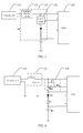
- the mobile terminal of the present disclosure comprises a charging port 110, a PMU 120, a battery B1 and a charging surge protection circuit 130.
- the charging port 110 is disposed on a case of the mobile terminal and allows a battery charger to be inserted therein.
- the PMU is a power management chip commonly used in a conventional mobile terminal.
- the charging surge protection circuit 130 is disposed between the charging port 110 and the PMU 120, and serves to eliminate the surge voltage in the battery charging process.
- the charging surge protection circuit 130 comprises a low-pass filtering circuit 131, a switch control circuit 132, a diode D1 and a first resistor R1.
- the PMU 120 comprises a first input terminal 1 for detecting whether the battery charger is plugged, a second input terminal 3 for detecting a charging current, a third input terminal 4 for detecting an input voltage of the battery and an output terminal 2 for controlling a charging switch.
- the charging port 110 has a first output terminal connected to an input terminal of the low-pass filtering circuit 131 and a second output terminal grounded; and an output terminal of the low-pass filtering circuit 131 is connected to the first input terminal 1 of the PMU 120.
- the low-pass filtering circuit 131 is a first-stage protection circuit of the mobile terminal, and is mainly used to attenuate the surge voltage generated during the battery charging process of the mobile terminal so as to significantly reduce the surge energy transmitted into the mobile terminal.
- the switch control circuit 132 has a first input terminal 5 connected to the output terminal of the low-pass filtering circuit 131, a second input terminal 6 connected to the output terminal 2 of the PMU 120, and an output terminal 7 connected to an anode of the diode D1.
- the switch control circuit 132 turns off the charging path of the mobile terminal in order to protect the back-end circuit.
- a cathode of the diode D1 is connected to an anode of the battery B1 via the first resistor R1, and is also connected to the second input terminal 3 of the PMU 120; and the second input terminal 3 is mainly used to detect the charging current flowing through the diode D1.
- a cathode of the battery B1 is grounded, and the anode of the battery B 1 is also connected to the third input terminal 4 of the PMU 120.
- the third input terminal 4 is mainly used to detect the voltage input of the battery B 1. When the battery is fully charged, the output terminal 2 of the PMU 120 is controlled to turn off the charging circuit.
- the low-pass filtering circuit 131 comprises an inductor L1 and a first capacitor C1.
- the inductor L1 is connected in series between the first output terminal of the charging port 110 and the first input terminal 1 of the PMU 120, and the first capacitor C1 has one end connected to the inductor L1 and the other end grounded.
- the aforesaid surge of 20 ns has a pulse frequency of 50 kHz, so the low-pass filtering circuit can greatly attenuate such a surge and can significantly reduce the surge energy transmitted into the mobile terminal.
- the value range of the voltage and that of the first capacitance may further be adjusted according to the frequency of the surge voltage that possibly occurs in practical applications.
- the switch control circuit 132 comprises an MOS transistor M1 and a second capacitor C2.
- the MOS transistor M1 has a source S connected to the first input terminal 1 of the PMU 120, a gate G connected to the output terminal 2 of the PMU 120, and a drain D connected to the anode of the diode D1.
- the MOS transistor is a P-channel MOS transistor, and mainly serves as a switch in the charging circuit of the mobile terminal.
- the second capacitor C2 is disposed between the source S and the gate G of the MOS transistor M1. That is, the second capacitor C2 has one end connected to the source S of the MOS transistor and the other end connected to the gate G of the MOS transistor.
- the second capacitor mainly has a coupling function in the switch control circuit.
- a second resistor R2 is further connected in series between the gate G of the MOS transistor M1 and the output terminal of the PMU 120.
- the second capacitor C2 is mainly used to couple the surge voltage from the source S of the MOS transistor M1 to the gate G and, thus, force the MOS transistor M1 to be turned off in order to protect the back-end circuit.
- the second resistor R2 is mainly used to provide a coupling potential of the gate G of the MOS transistor, and also serves to protect ports of the PMU 120.
- the charging current flows from the charging port 110 through the inductor L1, the MOS transistor M1, the diode D1, the first resistor R1 and the battery B1 in sequence.
- the individual ports and the battery of the mobile terminal are effectively protected through protection of the aforesaid two stages of protection circuits during the battery charging process of the mobile terminal.
- a charging surge protection circuit is disposed in the mobile terminal of the present disclosure for protection against the charging surge during the battery charging process of the mobile terminal.
- the charging surge protection circuit comprises a low-pass filtering circuit and a switch control circuit, so two surge voltage protection stages are achieved in the mobile terminal to effectively protect individual ports and the battery of the mobile terminal.
- the present disclosure only additionally provides one resistor, one capacitor and one inductor to constitute a two-stage charging protection circuit. Therefore, the present disclosure is relatively easy to be implemented in circuit, and has a relatively low cost.
Applications Claiming Priority (2)
| Application Number | Priority Date | Filing Date | Title |
|---|---|---|---|
| CN2010102427408A CN102196071B (zh) | 2010-07-30 | 2010-07-30 | 一种移动终端 |
| PCT/CN2011/072230 WO2012013046A1 (zh) | 2010-07-30 | 2011-03-29 | 一种移动终端 |
Publications (3)
| Publication Number | Publication Date |
|---|---|
| EP2600477A1 true EP2600477A1 (de) | 2013-06-05 |
| EP2600477A4 EP2600477A4 (de) | 2014-01-08 |
| EP2600477B1 EP2600477B1 (de) | 2018-04-25 |
Family
ID=44603430
Family Applications (1)
| Application Number | Title | Priority Date | Filing Date |
|---|---|---|---|
| EP11811748.0A Active EP2600477B1 (de) | 2010-07-30 | 2011-03-29 | Mobiles endgerät |
Country Status (5)
| Country | Link |
|---|---|
| US (1) | US9131036B2 (de) |
| EP (1) | EP2600477B1 (de) |
| CN (1) | CN102196071B (de) |
| ES (1) | ES2668781T3 (de) |
| WO (1) | WO2012013046A1 (de) |
Families Citing this family (6)
| Publication number | Priority date | Publication date | Assignee | Title |
|---|---|---|---|---|
| CN102611154B (zh) * | 2012-03-02 | 2015-07-15 | 惠州Tcl移动通信有限公司 | 一种具有抑制瞬态电压功能的充电电路及其手机 |
| CN103746427A (zh) * | 2014-01-09 | 2014-04-23 | 小米科技有限责任公司 | 电源、电源充电电路、方法及终端设备 |
| KR20160097592A (ko) | 2015-02-09 | 2016-08-18 | 한상길 | 포름알데히드와 암모니아를 제거하는 친환경 소취제 조성물 |
| CN104701946A (zh) * | 2015-03-25 | 2015-06-10 | 黎凯华 | 一种手机的浪涌保护电路 |
| MY182687A (en) * | 2015-06-01 | 2021-01-29 | Guangdong Oppo Mobile Telecommunications Corp Ltd | Charging circuit and mobile terminal |
| CN109831567B (zh) * | 2018-11-15 | 2021-01-19 | 芯海科技(深圳)股份有限公司 | 一种提高移动终端压力感应电源键的可靠性的方法及系统 |
Citations (3)
| Publication number | Priority date | Publication date | Assignee | Title |
|---|---|---|---|---|
| EP0444569A1 (de) * | 1990-02-28 | 1991-09-04 | Alcatel Cit | Vorrichtung zum Schutz gegen durch An- und Ausschaltung einer elektronischen Einheit an eine Gleichspannungsspeisung erzeugte Speisespannungsstörungen |
| US5986437A (en) * | 1996-12-17 | 1999-11-16 | Samsung Electronics Co., Ltd. | Power supply system for portable electronic devices |
| KR20020026084A (ko) * | 2000-09-30 | 2002-04-06 | 김병홍 | 휴대용 다전원 충전기 |
Family Cites Families (7)
| Publication number | Priority date | Publication date | Assignee | Title |
|---|---|---|---|---|
| US3382377A (en) * | 1964-01-13 | 1968-05-07 | Gen Signal Corp | Polarity shift receiver |
| EP1253696A1 (de) * | 2001-04-25 | 2002-10-30 | TELEFONAKTIEBOLAGET L M ERICSSON (publ) | Verfahren zur Batterieladung |
| WO2006001088A1 (ja) * | 2004-06-24 | 2006-01-05 | Firac International Co., Ltd. | 太陽電池式充電装置 |
| TW200849782A (en) * | 2007-06-12 | 2008-12-16 | Richtek Technology Corp | Device and method to suppress input current spike of voltage converter in a precharging mode |
| CN101453128B (zh) * | 2007-11-30 | 2011-03-16 | 希姆通信息技术(上海)有限公司 | 手机充电电路及其充电方法 |
| TWI367459B (en) * | 2008-04-25 | 2012-07-01 | Chimei Innolux Corp | Alarm system |
| KR101271432B1 (ko) * | 2009-12-21 | 2013-06-05 | 한국전자통신연구원 | 주파수 혼합기 |
-
2010
- 2010-07-30 CN CN2010102427408A patent/CN102196071B/zh active Active
-
2011
- 2011-03-29 EP EP11811748.0A patent/EP2600477B1/de active Active
- 2011-03-29 ES ES11811748.0T patent/ES2668781T3/es active Active
- 2011-03-29 US US13/807,007 patent/US9131036B2/en not_active Expired - Fee Related
- 2011-03-29 WO PCT/CN2011/072230 patent/WO2012013046A1/zh active Application Filing
Patent Citations (3)
| Publication number | Priority date | Publication date | Assignee | Title |
|---|---|---|---|---|
| EP0444569A1 (de) * | 1990-02-28 | 1991-09-04 | Alcatel Cit | Vorrichtung zum Schutz gegen durch An- und Ausschaltung einer elektronischen Einheit an eine Gleichspannungsspeisung erzeugte Speisespannungsstörungen |
| US5986437A (en) * | 1996-12-17 | 1999-11-16 | Samsung Electronics Co., Ltd. | Power supply system for portable electronic devices |
| KR20020026084A (ko) * | 2000-09-30 | 2002-04-06 | 김병홍 | 휴대용 다전원 충전기 |
Non-Patent Citations (1)
| Title |
|---|
| See also references of WO2012013046A1 * |
Also Published As
| Publication number | Publication date |
|---|---|
| EP2600477A4 (de) | 2014-01-08 |
| EP2600477B1 (de) | 2018-04-25 |
| CN102196071A (zh) | 2011-09-21 |
| US9131036B2 (en) | 2015-09-08 |
| ES2668781T3 (es) | 2018-05-22 |
| WO2012013046A1 (zh) | 2012-02-02 |
| US20130109444A1 (en) | 2013-05-02 |
| CN102196071B (zh) | 2013-02-20 |
Similar Documents
| Publication | Publication Date | Title |
|---|---|---|
| EP2600477A1 (de) | Mobiles endgerät | |
| US10734826B2 (en) | Power supply including bi-directional DC converter and control method thereof | |
| TWI680626B (zh) | 受電裝置及其控制電路、電子機器、供電系統之動作方法 | |
| KR102296479B1 (ko) | 충전 회로, 단말 및 충전 방법 | |
| US11183863B2 (en) | Charging apparatus and terminal | |
| US7902794B2 (en) | Over-voltage protected battery charger with bypass | |
| CN103545803B (zh) | 设备电源接口电路保护装置 | |
| US20210359532A1 (en) | Charging circuit and electronic device | |
| WO2018090924A1 (zh) | 过压和反接保护电路及其设备 | |
| US20160204712A1 (en) | Ac-dc conversion circuit | |
| US8730689B2 (en) | Capacitive power supply | |
| CN109980722B (zh) | 一种电源控制装置 | |
| CN201839323U (zh) | 一种具有浪涌保护电路的移动终端 | |
| CN110445216B (zh) | 一种充电芯片 | |
| CN103701165B (zh) | 一种激活移动电源的方法及装置 | |
| CN101458901B (zh) | 液晶显示器的供电电路 | |
| CN105162078B (zh) | 一种终端的充电保护电路及方法和终端 | |
| US20140111014A1 (en) | Charging and discharging system and method for battery | |
| US11437811B2 (en) | Electronic device | |
| KR20140074167A (ko) | 범용 전원 공급 장치 | |
| US20160241062A1 (en) | Electrical power converter circuits | |
| CN1157835C (zh) | 稳压及电源电压侦测保护电路装置 | |
| CN203014356U (zh) | 功率管的短路保护电路 | |
| CN108718149A (zh) | 供电电路及电子设备 | |
| KR100478358B1 (ko) | 배터리 관리용 아이씨의 정전기 방전에 대한 보호 회로 |
Legal Events
| Date | Code | Title | Description |
|---|---|---|---|
| PUAI | Public reference made under article 153(3) epc to a published international application that has entered the european phase |
Free format text: ORIGINAL CODE: 0009012 |
|
| 17P | Request for examination filed |
Effective date: 20121221 |
|
| AK | Designated contracting states |
Kind code of ref document: A1 Designated state(s): AL AT BE BG CH CY CZ DE DK EE ES FI FR GB GR HR HU IE IS IT LI LT LU LV MC MK MT NL NO PL PT RO RS SE SI SK SM TR |
|
| DAX | Request for extension of the european patent (deleted) | ||
| A4 | Supplementary search report drawn up and despatched |
Effective date: 20131206 |
|
| RIC1 | Information provided on ipc code assigned before grant |
Ipc: H02J 7/00 20060101ALI20131202BHEP Ipc: H02H 7/18 20060101ALN20131202BHEP Ipc: H02H 9/04 20060101AFI20131202BHEP Ipc: H04M 1/02 20060101ALN20131202BHEP |
|
| 17Q | First examination report despatched |
Effective date: 20160309 |
|
| STAA | Information on the status of an ep patent application or granted ep patent |
Free format text: STATUS: EXAMINATION IS IN PROGRESS |
|
| GRAP | Despatch of communication of intention to grant a patent |
Free format text: ORIGINAL CODE: EPIDOSNIGR1 |
|
| STAA | Information on the status of an ep patent application or granted ep patent |
Free format text: STATUS: GRANT OF PATENT IS INTENDED |
|
| RIC1 | Information provided on ipc code assigned before grant |
Ipc: H02H 7/18 20060101ALN20171016BHEP Ipc: H04M 1/02 20060101ALN20171016BHEP Ipc: H02H 9/04 20060101AFI20171016BHEP Ipc: H02J 7/00 20060101ALI20171016BHEP |
|
| INTG | Intention to grant announced |
Effective date: 20171103 |
|
| GRAS | Grant fee paid |
Free format text: ORIGINAL CODE: EPIDOSNIGR3 |
|
| GRAA | (expected) grant |
Free format text: ORIGINAL CODE: 0009210 |
|
| STAA | Information on the status of an ep patent application or granted ep patent |
Free format text: STATUS: THE PATENT HAS BEEN GRANTED |
|
| AK | Designated contracting states |
Kind code of ref document: B1 Designated state(s): AL AT BE BG CH CY CZ DE DK EE ES FI FR GB GR HR HU IE IS IT LI LT LU LV MC MK MT NL NO PL PT RO RS SE SI SK SM TR |
|
| REG | Reference to a national code |
Ref country code: GB Ref legal event code: FG4D |
|
| REG | Reference to a national code |
Ref country code: CH Ref legal event code: EP |
|
| REG | Reference to a national code |
Ref country code: AT Ref legal event code: REF Ref document number: 993852 Country of ref document: AT Kind code of ref document: T Effective date: 20180515 |
|
| REG | Reference to a national code |
Ref country code: IE Ref legal event code: FG4D |
|
| REG | Reference to a national code |
Ref country code: DE Ref legal event code: R096 Ref document number: 602011047885 Country of ref document: DE |
|
| REG | Reference to a national code |
Ref country code: ES Ref legal event code: FG2A Ref document number: 2668781 Country of ref document: ES Kind code of ref document: T3 Effective date: 20180522 |
|
| REG | Reference to a national code |
Ref country code: NL Ref legal event code: MP Effective date: 20180425 |
|
| REG | Reference to a national code |
Ref country code: LT Ref legal event code: MG4D |
|
| PG25 | Lapsed in a contracting state [announced via postgrant information from national office to epo] |
Ref country code: NL Free format text: LAPSE BECAUSE OF FAILURE TO SUBMIT A TRANSLATION OF THE DESCRIPTION OR TO PAY THE FEE WITHIN THE PRESCRIBED TIME-LIMIT Effective date: 20180425 |
|
| PG25 | Lapsed in a contracting state [announced via postgrant information from national office to epo] |
Ref country code: BG Free format text: LAPSE BECAUSE OF FAILURE TO SUBMIT A TRANSLATION OF THE DESCRIPTION OR TO PAY THE FEE WITHIN THE PRESCRIBED TIME-LIMIT Effective date: 20180725 Ref country code: FI Free format text: LAPSE BECAUSE OF FAILURE TO SUBMIT A TRANSLATION OF THE DESCRIPTION OR TO PAY THE FEE WITHIN THE PRESCRIBED TIME-LIMIT Effective date: 20180425 Ref country code: PL Free format text: LAPSE BECAUSE OF FAILURE TO SUBMIT A TRANSLATION OF THE DESCRIPTION OR TO PAY THE FEE WITHIN THE PRESCRIBED TIME-LIMIT Effective date: 20180425 Ref country code: LT Free format text: LAPSE BECAUSE OF FAILURE TO SUBMIT A TRANSLATION OF THE DESCRIPTION OR TO PAY THE FEE WITHIN THE PRESCRIBED TIME-LIMIT Effective date: 20180425 Ref country code: SE Free format text: LAPSE BECAUSE OF FAILURE TO SUBMIT A TRANSLATION OF THE DESCRIPTION OR TO PAY THE FEE WITHIN THE PRESCRIBED TIME-LIMIT Effective date: 20180425 Ref country code: NO Free format text: LAPSE BECAUSE OF FAILURE TO SUBMIT A TRANSLATION OF THE DESCRIPTION OR TO PAY THE FEE WITHIN THE PRESCRIBED TIME-LIMIT Effective date: 20180725 |
|
| PG25 | Lapsed in a contracting state [announced via postgrant information from national office to epo] |
Ref country code: HR Free format text: LAPSE BECAUSE OF FAILURE TO SUBMIT A TRANSLATION OF THE DESCRIPTION OR TO PAY THE FEE WITHIN THE PRESCRIBED TIME-LIMIT Effective date: 20180425 Ref country code: GR Free format text: LAPSE BECAUSE OF FAILURE TO SUBMIT A TRANSLATION OF THE DESCRIPTION OR TO PAY THE FEE WITHIN THE PRESCRIBED TIME-LIMIT Effective date: 20180726 Ref country code: LV Free format text: LAPSE BECAUSE OF FAILURE TO SUBMIT A TRANSLATION OF THE DESCRIPTION OR TO PAY THE FEE WITHIN THE PRESCRIBED TIME-LIMIT Effective date: 20180425 Ref country code: RS Free format text: LAPSE BECAUSE OF FAILURE TO SUBMIT A TRANSLATION OF THE DESCRIPTION OR TO PAY THE FEE WITHIN THE PRESCRIBED TIME-LIMIT Effective date: 20180425 |
|
| REG | Reference to a national code |
Ref country code: AT Ref legal event code: MK05 Ref document number: 993852 Country of ref document: AT Kind code of ref document: T Effective date: 20180425 |
|
| PG25 | Lapsed in a contracting state [announced via postgrant information from national office to epo] |
Ref country code: PT Free format text: LAPSE BECAUSE OF FAILURE TO SUBMIT A TRANSLATION OF THE DESCRIPTION OR TO PAY THE FEE WITHIN THE PRESCRIBED TIME-LIMIT Effective date: 20180827 |
|
| REG | Reference to a national code |
Ref country code: DE Ref legal event code: R097 Ref document number: 602011047885 Country of ref document: DE |
|
| PG25 | Lapsed in a contracting state [announced via postgrant information from national office to epo] |
Ref country code: SK Free format text: LAPSE BECAUSE OF FAILURE TO SUBMIT A TRANSLATION OF THE DESCRIPTION OR TO PAY THE FEE WITHIN THE PRESCRIBED TIME-LIMIT Effective date: 20180425 Ref country code: EE Free format text: LAPSE BECAUSE OF FAILURE TO SUBMIT A TRANSLATION OF THE DESCRIPTION OR TO PAY THE FEE WITHIN THE PRESCRIBED TIME-LIMIT Effective date: 20180425 Ref country code: CZ Free format text: LAPSE BECAUSE OF FAILURE TO SUBMIT A TRANSLATION OF THE DESCRIPTION OR TO PAY THE FEE WITHIN THE PRESCRIBED TIME-LIMIT Effective date: 20180425 Ref country code: RO Free format text: LAPSE BECAUSE OF FAILURE TO SUBMIT A TRANSLATION OF THE DESCRIPTION OR TO PAY THE FEE WITHIN THE PRESCRIBED TIME-LIMIT Effective date: 20180425 Ref country code: AT Free format text: LAPSE BECAUSE OF FAILURE TO SUBMIT A TRANSLATION OF THE DESCRIPTION OR TO PAY THE FEE WITHIN THE PRESCRIBED TIME-LIMIT Effective date: 20180425 Ref country code: DK Free format text: LAPSE BECAUSE OF FAILURE TO SUBMIT A TRANSLATION OF THE DESCRIPTION OR TO PAY THE FEE WITHIN THE PRESCRIBED TIME-LIMIT Effective date: 20180425 |
|
| PG25 | Lapsed in a contracting state [announced via postgrant information from national office to epo] |
Ref country code: SM Free format text: LAPSE BECAUSE OF FAILURE TO SUBMIT A TRANSLATION OF THE DESCRIPTION OR TO PAY THE FEE WITHIN THE PRESCRIBED TIME-LIMIT Effective date: 20180425 |
|
| PLBE | No opposition filed within time limit |
Free format text: ORIGINAL CODE: 0009261 |
|
| STAA | Information on the status of an ep patent application or granted ep patent |
Free format text: STATUS: NO OPPOSITION FILED WITHIN TIME LIMIT |
|
| 26N | No opposition filed |
Effective date: 20190128 |
|
| PG25 | Lapsed in a contracting state [announced via postgrant information from national office to epo] |
Ref country code: SI Free format text: LAPSE BECAUSE OF FAILURE TO SUBMIT A TRANSLATION OF THE DESCRIPTION OR TO PAY THE FEE WITHIN THE PRESCRIBED TIME-LIMIT Effective date: 20180425 |
|
| PG25 | Lapsed in a contracting state [announced via postgrant information from national office to epo] |
Ref country code: MC Free format text: LAPSE BECAUSE OF FAILURE TO SUBMIT A TRANSLATION OF THE DESCRIPTION OR TO PAY THE FEE WITHIN THE PRESCRIBED TIME-LIMIT Effective date: 20180425 |
|
| REG | Reference to a national code |
Ref country code: CH Ref legal event code: PL |
|
| PG25 | Lapsed in a contracting state [announced via postgrant information from national office to epo] |
Ref country code: AL Free format text: LAPSE BECAUSE OF FAILURE TO SUBMIT A TRANSLATION OF THE DESCRIPTION OR TO PAY THE FEE WITHIN THE PRESCRIBED TIME-LIMIT Effective date: 20180425 Ref country code: LU Free format text: LAPSE BECAUSE OF NON-PAYMENT OF DUE FEES Effective date: 20190329 |
|
| REG | Reference to a national code |
Ref country code: BE Ref legal event code: MM Effective date: 20190331 |
|
| PG25 | Lapsed in a contracting state [announced via postgrant information from national office to epo] |
Ref country code: CH Free format text: LAPSE BECAUSE OF NON-PAYMENT OF DUE FEES Effective date: 20190331 Ref country code: IE Free format text: LAPSE BECAUSE OF NON-PAYMENT OF DUE FEES Effective date: 20190329 Ref country code: LI Free format text: LAPSE BECAUSE OF NON-PAYMENT OF DUE FEES Effective date: 20190331 |
|
| PG25 | Lapsed in a contracting state [announced via postgrant information from national office to epo] |
Ref country code: BE Free format text: LAPSE BECAUSE OF NON-PAYMENT OF DUE FEES Effective date: 20190331 |
|
| PG25 | Lapsed in a contracting state [announced via postgrant information from national office to epo] |
Ref country code: TR Free format text: LAPSE BECAUSE OF FAILURE TO SUBMIT A TRANSLATION OF THE DESCRIPTION OR TO PAY THE FEE WITHIN THE PRESCRIBED TIME-LIMIT Effective date: 20180425 |
|
| PG25 | Lapsed in a contracting state [announced via postgrant information from national office to epo] |
Ref country code: MT Free format text: LAPSE BECAUSE OF NON-PAYMENT OF DUE FEES Effective date: 20190329 |
|
| PG25 | Lapsed in a contracting state [announced via postgrant information from national office to epo] |
Ref country code: CY Free format text: LAPSE BECAUSE OF FAILURE TO SUBMIT A TRANSLATION OF THE DESCRIPTION OR TO PAY THE FEE WITHIN THE PRESCRIBED TIME-LIMIT Effective date: 20180425 |
|
| PG25 | Lapsed in a contracting state [announced via postgrant information from national office to epo] |
Ref country code: IS Free format text: LAPSE BECAUSE OF FAILURE TO SUBMIT A TRANSLATION OF THE DESCRIPTION OR TO PAY THE FEE WITHIN THE PRESCRIBED TIME-LIMIT Effective date: 20180825 |
|
| PG25 | Lapsed in a contracting state [announced via postgrant information from national office to epo] |
Ref country code: HU Free format text: LAPSE BECAUSE OF FAILURE TO SUBMIT A TRANSLATION OF THE DESCRIPTION OR TO PAY THE FEE WITHIN THE PRESCRIBED TIME-LIMIT; INVALID AB INITIO Effective date: 20110329 |
|
| PGFP | Annual fee paid to national office [announced via postgrant information from national office to epo] |
Ref country code: ES Payment date: 20210525 Year of fee payment: 11 |
|
| PGFP | Annual fee paid to national office [announced via postgrant information from national office to epo] |
Ref country code: GB Payment date: 20220321 Year of fee payment: 12 Ref country code: DE Payment date: 20220322 Year of fee payment: 12 |
|
| PGFP | Annual fee paid to national office [announced via postgrant information from national office to epo] |
Ref country code: IT Payment date: 20220322 Year of fee payment: 12 Ref country code: FR Payment date: 20220322 Year of fee payment: 12 |
|
| PG25 | Lapsed in a contracting state [announced via postgrant information from national office to epo] |
Ref country code: MK Free format text: LAPSE BECAUSE OF FAILURE TO SUBMIT A TRANSLATION OF THE DESCRIPTION OR TO PAY THE FEE WITHIN THE PRESCRIBED TIME-LIMIT Effective date: 20180425 |
|
| REG | Reference to a national code |
Ref country code: ES Ref legal event code: FD2A Effective date: 20230526 |
|
| PG25 | Lapsed in a contracting state [announced via postgrant information from national office to epo] |
Ref country code: ES Free format text: LAPSE BECAUSE OF NON-PAYMENT OF DUE FEES Effective date: 20220330 |
|
| REG | Reference to a national code |
Ref country code: DE Ref legal event code: R119 Ref document number: 602011047885 Country of ref document: DE |
|
| GBPC | Gb: european patent ceased through non-payment of renewal fee |
Effective date: 20230329 |
|
| PG25 | Lapsed in a contracting state [announced via postgrant information from national office to epo] |
Ref country code: GB Free format text: LAPSE BECAUSE OF NON-PAYMENT OF DUE FEES Effective date: 20230329 |
|
| PG25 | Lapsed in a contracting state [announced via postgrant information from national office to epo] |
Ref country code: GB Free format text: LAPSE BECAUSE OF NON-PAYMENT OF DUE FEES Effective date: 20230329 Ref country code: FR Free format text: LAPSE BECAUSE OF NON-PAYMENT OF DUE FEES Effective date: 20230331 Ref country code: DE Free format text: LAPSE BECAUSE OF NON-PAYMENT OF DUE FEES Effective date: 20231003 |