EP2599746A1 - Verfahren zur Herstellung einer Struktur mit mindestens einem aus mehreren Dicken bestehenden aktiven Teil - Google Patents
Verfahren zur Herstellung einer Struktur mit mindestens einem aus mehreren Dicken bestehenden aktiven Teil Download PDFInfo
- Publication number
- EP2599746A1 EP2599746A1 EP12194881.4A EP12194881A EP2599746A1 EP 2599746 A1 EP2599746 A1 EP 2599746A1 EP 12194881 A EP12194881 A EP 12194881A EP 2599746 A1 EP2599746 A1 EP 2599746A1
- Authority
- EP
- European Patent Office
- Prior art keywords
- substrate
- layer
- semiconductor material
- production method
- zone
- Prior art date
- Legal status (The legal status is an assumption and is not a legal conclusion. Google has not performed a legal analysis and makes no representation as to the accuracy of the status listed.)
- Granted
Links
- 238000000034 method Methods 0.000 title claims abstract description 43
- 239000000758 substrate Substances 0.000 claims abstract description 122
- 239000004065 semiconductor Substances 0.000 claims abstract description 74
- 239000000463 material Substances 0.000 claims abstract description 71
- 238000005530 etching Methods 0.000 claims description 44
- 238000004519 manufacturing process Methods 0.000 claims description 33
- 238000007789 sealing Methods 0.000 claims description 29
- 229910052710 silicon Inorganic materials 0.000 claims description 28
- 239000010703 silicon Substances 0.000 claims description 28
- 238000000151 deposition Methods 0.000 claims description 21
- 238000000407 epitaxy Methods 0.000 claims description 20
- 238000007254 oxidation reaction Methods 0.000 claims description 19
- 230000003647 oxidation Effects 0.000 claims description 16
- 238000003754 machining Methods 0.000 claims description 15
- 238000001459 lithography Methods 0.000 claims description 13
- 230000008021 deposition Effects 0.000 claims description 11
- 239000011148 porous material Substances 0.000 claims description 11
- 238000005498 polishing Methods 0.000 claims description 10
- 229910004298 SiO 2 Inorganic materials 0.000 claims description 9
- 230000015572 biosynthetic process Effects 0.000 claims description 8
- 238000005755 formation reaction Methods 0.000 claims description 8
- 239000000126 substance Substances 0.000 claims description 8
- 238000001039 wet etching Methods 0.000 claims description 6
- FGUUSXIOTUKUDN-IBGZPJMESA-N C1(=CC=CC=C1)N1C2=C(NC([C@H](C1)NC=1OC(=NN=1)C1=CC=CC=C1)=O)C=CC=C2 Chemical compound C1(=CC=CC=C1)N1C2=C(NC([C@H](C1)NC=1OC(=NN=1)C1=CC=CC=C1)=O)C=CC=C2 FGUUSXIOTUKUDN-IBGZPJMESA-N 0.000 claims description 5
- 238000000137 annealing Methods 0.000 claims description 4
- 230000008030 elimination Effects 0.000 claims description 4
- 238000003379 elimination reaction Methods 0.000 claims description 4
- 238000005299 abrasion Methods 0.000 claims description 3
- 230000008018 melting Effects 0.000 claims description 3
- 238000002844 melting Methods 0.000 claims description 3
- 239000004020 conductor Substances 0.000 claims description 2
- 239000000543 intermediate Substances 0.000 claims 5
- 229910021421 monocrystalline silicon Inorganic materials 0.000 abstract description 9
- 230000001590 oxidative effect Effects 0.000 abstract 1
- 239000010410 layer Substances 0.000 description 140
- XUIMIQQOPSSXEZ-UHFFFAOYSA-N Silicon Chemical compound [Si] XUIMIQQOPSSXEZ-UHFFFAOYSA-N 0.000 description 36
- 229910021426 porous silicon Inorganic materials 0.000 description 24
- 101100460147 Sarcophaga bullata NEMS gene Proteins 0.000 description 21
- KRHYYFGTRYWZRS-UHFFFAOYSA-N Fluorane Chemical compound F KRHYYFGTRYWZRS-UHFFFAOYSA-N 0.000 description 12
- 238000000708 deep reactive-ion etching Methods 0.000 description 9
- 229910000577 Silicon-germanium Inorganic materials 0.000 description 6
- WGTYBPLFGIVFAS-UHFFFAOYSA-M tetramethylammonium hydroxide Chemical compound [OH-].C[N+](C)(C)C WGTYBPLFGIVFAS-UHFFFAOYSA-M 0.000 description 4
- 230000000694 effects Effects 0.000 description 3
- 238000000227 grinding Methods 0.000 description 3
- 229910021420 polycrystalline silicon Inorganic materials 0.000 description 3
- 229920005591 polysilicon Polymers 0.000 description 3
- GNFTZDOKVXKIBK-UHFFFAOYSA-N 3-(2-methoxyethoxy)benzohydrazide Chemical compound COCCOC1=CC=CC(C(=O)NN)=C1 GNFTZDOKVXKIBK-UHFFFAOYSA-N 0.000 description 2
- 229910052581 Si3N4 Inorganic materials 0.000 description 2
- 238000006073 displacement reaction Methods 0.000 description 2
- 238000005516 engineering process Methods 0.000 description 2
- 230000005496 eutectics Effects 0.000 description 2
- 150000002500 ions Chemical class 0.000 description 2
- 239000012528 membrane Substances 0.000 description 2
- 238000000206 photolithography Methods 0.000 description 2
- 238000005096 rolling process Methods 0.000 description 2
- HQVNEWCFYHHQES-UHFFFAOYSA-N silicon nitride Chemical compound N12[Si]34N5[Si]62N3[Si]51N64 HQVNEWCFYHHQES-UHFFFAOYSA-N 0.000 description 2
- RZVAJINKPMORJF-UHFFFAOYSA-N Acetaminophen Chemical compound CC(=O)NC1=CC=C(O)C=C1 RZVAJINKPMORJF-UHFFFAOYSA-N 0.000 description 1
- UFHFLCQGNIYNRP-UHFFFAOYSA-N Hydrogen Chemical compound [H][H] UFHFLCQGNIYNRP-UHFFFAOYSA-N 0.000 description 1
- 229910008310 Si—Ge Inorganic materials 0.000 description 1
- 230000001133 acceleration Effects 0.000 description 1
- 230000003466 anti-cipated effect Effects 0.000 description 1
- 238000012550 audit Methods 0.000 description 1
- 238000003486 chemical etching Methods 0.000 description 1
- SLLGVCUQYRMELA-UHFFFAOYSA-N chlorosilicon Chemical compound Cl[Si] SLLGVCUQYRMELA-UHFFFAOYSA-N 0.000 description 1
- 239000011248 coating agent Substances 0.000 description 1
- 238000000576 coating method Methods 0.000 description 1
- 239000013078 crystal Substances 0.000 description 1
- 230000007547 defect Effects 0.000 description 1
- 239000011521 glass Substances 0.000 description 1
- 229910052739 hydrogen Inorganic materials 0.000 description 1
- 239000001257 hydrogen Substances 0.000 description 1
- 239000012212 insulator Substances 0.000 description 1
- 239000002184 metal Substances 0.000 description 1
- 150000004767 nitrides Chemical class 0.000 description 1
- 239000005297 pyrex Substances 0.000 description 1
- 238000011084 recovery Methods 0.000 description 1
- 239000002344 surface layer Substances 0.000 description 1
- 239000012808 vapor phase Substances 0.000 description 1
Images


Classifications
-
- H—ELECTRICITY
- H01—ELECTRIC ELEMENTS
- H01L—SEMICONDUCTOR DEVICES NOT COVERED BY CLASS H10
- H01L21/00—Processes or apparatus adapted for the manufacture or treatment of semiconductor or solid state devices or of parts thereof
- H01L21/02—Manufacture or treatment of semiconductor devices or of parts thereof
- H01L21/04—Manufacture or treatment of semiconductor devices or of parts thereof the devices having at least one potential-jump barrier or surface barrier, e.g. PN junction, depletion layer or carrier concentration layer
- H01L21/18—Manufacture or treatment of semiconductor devices or of parts thereof the devices having at least one potential-jump barrier or surface barrier, e.g. PN junction, depletion layer or carrier concentration layer the devices having semiconductor bodies comprising elements of Group IV of the Periodic System or AIIIBV compounds with or without impurities, e.g. doping materials
- H01L21/20—Deposition of semiconductor materials on a substrate, e.g. epitaxial growth solid phase epitaxy
-
- B—PERFORMING OPERATIONS; TRANSPORTING
- B81—MICROSTRUCTURAL TECHNOLOGY
- B81C—PROCESSES OR APPARATUS SPECIALLY ADAPTED FOR THE MANUFACTURE OR TREATMENT OF MICROSTRUCTURAL DEVICES OR SYSTEMS
- B81C1/00—Manufacture or treatment of devices or systems in or on a substrate
- B81C1/00436—Shaping materials, i.e. techniques for structuring the substrate or the layers on the substrate
- B81C1/00555—Achieving a desired geometry, i.e. controlling etch rates, anisotropy or selectivity
- B81C1/00626—Processes for achieving a desired geometry not provided for in groups B81C1/00563 - B81C1/00619
-
- G—PHYSICS
- G01—MEASURING; TESTING
- G01P—MEASURING LINEAR OR ANGULAR SPEED, ACCELERATION, DECELERATION, OR SHOCK; INDICATING PRESENCE, ABSENCE, OR DIRECTION, OF MOVEMENT
- G01P15/00—Measuring acceleration; Measuring deceleration; Measuring shock, i.e. sudden change of acceleration
- G01P15/02—Measuring acceleration; Measuring deceleration; Measuring shock, i.e. sudden change of acceleration by making use of inertia forces using solid seismic masses
- G01P15/08—Measuring acceleration; Measuring deceleration; Measuring shock, i.e. sudden change of acceleration by making use of inertia forces using solid seismic masses with conversion into electric or magnetic values
- G01P15/0802—Details
-
- B—PERFORMING OPERATIONS; TRANSPORTING
- B81—MICROSTRUCTURAL TECHNOLOGY
- B81B—MICROSTRUCTURAL DEVICES OR SYSTEMS, e.g. MICROMECHANICAL DEVICES
- B81B2203/00—Basic microelectromechanical structures
- B81B2203/01—Suspended structures, i.e. structures allowing a movement
- B81B2203/0109—Bridges
-
- B—PERFORMING OPERATIONS; TRANSPORTING
- B81—MICROSTRUCTURAL TECHNOLOGY
- B81B—MICROSTRUCTURAL DEVICES OR SYSTEMS, e.g. MICROMECHANICAL DEVICES
- B81B2203/00—Basic microelectromechanical structures
- B81B2203/01—Suspended structures, i.e. structures allowing a movement
- B81B2203/0118—Cantilevers
-
- B—PERFORMING OPERATIONS; TRANSPORTING
- B81—MICROSTRUCTURAL TECHNOLOGY
- B81C—PROCESSES OR APPARATUS SPECIALLY ADAPTED FOR THE MANUFACTURE OR TREATMENT OF MICROSTRUCTURAL DEVICES OR SYSTEMS
- B81C2201/00—Manufacture or treatment of microstructural devices or systems
- B81C2201/01—Manufacture or treatment of microstructural devices or systems in or on a substrate
- B81C2201/0101—Shaping material; Structuring the bulk substrate or layers on the substrate; Film patterning
- B81C2201/0111—Bulk micromachining
- B81C2201/0115—Porous silicon
-
- B—PERFORMING OPERATIONS; TRANSPORTING
- B81—MICROSTRUCTURAL TECHNOLOGY
- B81C—PROCESSES OR APPARATUS SPECIALLY ADAPTED FOR THE MANUFACTURE OR TREATMENT OF MICROSTRUCTURAL DEVICES OR SYSTEMS
- B81C2201/00—Manufacture or treatment of microstructural devices or systems
- B81C2201/01—Manufacture or treatment of microstructural devices or systems in or on a substrate
- B81C2201/0174—Manufacture or treatment of microstructural devices or systems in or on a substrate for making multi-layered devices, film deposition or growing
- B81C2201/019—Bonding or gluing multiple substrate layers
Definitions
- the present invention relates to a method for producing a structure comprising at least one multi-thickness active portion that can be implemented in the production of microelectromechanical systems (MEMS or "microelectromechanical systems” in English terminology) and / or systems nanoelectromechanical (NEMS or “nanoelectromechanical systems” in English terminology) for the realization for example of sensors or actuators.
- MEMS microelectromechanical systems
- NEMS nanoelectromechanical systems
- the MEMS and NEMS sensors comprise a fixed part and at least one part suspended relative to the fixed part, the suspended part or parts called “active parts” are able to move and / or to deform under the effect of an action external, such as mechanical, electrical, magnetic action.
- the displacement and / or the deformation of the moving part with respect to the fixed part makes it possible, for example, to determine an acceleration in the case of an accelerometer or a Coriolis force in the case of a gyrometer.
- the displacement of the moving part is for example measured by means of a strain gauge.
- the method of producing such an active part is made from a SOI type substrate ("Silicon on Insulator") which has a high cost.
- a thick epitaxial growth step is implemented, such a step is usually long and expensive.
- the strain gauge is formed from the SOI substrate and the seismic mass is formed from the SOI substrate and the thick epitaxial layer.
- the step of defining the active part uses an oxide layer on which the epitaxial growth will partly take place.
- the layer formed by epitaxy on the oxide layer is not monocrystalline in the interface areas between the two thicknesses, which were protected by the oxide layer. These "poly-crystalline" zones can generate defects in the structure.
- the epitaxial growth rate is different between the areas where the growth is on monocrystalline silicon and the areas where the growth is on the oxide layer, for example, which forms the interface of the two thicknesses. This difference in growth rate can lead to inhomogeneities of considerable thickness in the final structure.
- the object of the present invention is achieved by a method for producing a structure provided with a multilayer active part, comprising a step of epitaxially growing a monocrystalline semiconductor material on a substrate, at least the face on which the epitaxy is made of monocrystalline semiconductor material, the substrate having at least one zone in which the semiconductor material is discontinuous.
- zone in which the semiconductor material is discontinuous is intended to mean an area formed either by a porous material or by a plurality of thin semi-conductor material abutments arranged at a small distance from each other. others.
- the epitaxial step serves to form the first active layer similar to that formed from an SOI substrate.
- This first layer is usually thin.
- the second active layer generally thicker than the first, is advantageously formed by all or part of the "bulk" portion of the first substrate after sealing of a second substrate, whereas in the known method using an SOI substrate, this second active layer is formed by epitaxy. The disadvantages of thick epitaxy are thus avoided.
- the epitaxial layer which is monocrystalline, grows on a porous layer that can be removed selectively relative to the epitaxial layer, and therefore the porous layer acts as a sacrificial layer.
- the appearance of polycrystalline zones at the interfaces does not appear and the growth rates are substantially uniform between the discontinuous semiconductor material and the semiconductor material. monocrystalline substrate.
- the production method according to the invention does not require the use of an SOI substrate and does not implement thick epitaxy, this results in a gain in manufacturing cost and time.
- the inhomogeneities of thickness are reduced, it is not necessary to have a significant chemical-mechanical polishing step to make up for differences in thickness.
- the latter has pores of very small surface size, which improves the quality of the silicon which grows epitaxially on this porous zone, the pores of larger in-depth size, which allows selective etching or faster oxidation.
- step e) the formation of the sacrificial layer takes place at least on the front face and has the effect of completely or partially embedding the first suspended zone.
- the epitaxial growth step can be carried out in the same material as the semiconductor material of the front face of the first substrate or in another semiconductor material preferably having a mesh parameter close to that of the material of said face. .
- the formation of the sacrificial layer is for example obtained by depositing an oxide and / or by thermal oxidation.
- the method may advantageously comprise, after step e) and before step f), a step e ') of sealing or depositing a second substrate on the front face of the first substrate.
- a porous semiconductor material zone is produced.
- the porous semiconductor material zone can be obtained by electrochemical etching.
- the porous semiconductor material zone has pores of smaller surface size and larger pores of greater depth.
- the porous semiconductor material can be removed by etching, for example by wet etching, or by thermal oxidation of the porous semiconductor material and by etching the oxidized porous semiconductor material, by example by wet etching and / or steam.
- the elimination of the semiconductor material forming the pillars during step d) is obtained by annealing at a temperature close to the melting temperature of said material.
- the method comprises, prior to step e '), a step of structuring the second substrate.
- a face of the second substrate is etched so as to produce mechanical stops for the second suspended part and a deposit is made on said structured face of a layer intended to form a sealing layer during the step of sealing the second substrate.
- the process may comprise, following step e), the step of structuring the sacrificial layer and / or depositing one or more several intermediate layers on said sacrificial layer, said intermediate layers being structurable.
- the structuring of the sacrificial layer and of the intermediate layer or layers may be carried out, for example, by lithography and etching respectively of the sacrificial layer with a stop on the substrate and of the intermediate layer or layers with stopping on the sacrificial layer.
- the method may comprise a step of depositing a SiO 2 layer, planarization on the structured sacrificial layer and / or the intermediate layer or layers, said SiO 2 layer participating in the sealing.
- Sealing of the first and second substrates can be achieved by direct sealing or eutectic sealing.
- the first substrate is structured before step a).
- the first substrate and / or the second substrate may or may be thinned by abrasion on the backside and then chemo-chemical polishing.
- the method may comprise, prior to step a), a step of forming on the front face of the substrate a porous semiconductor layer and epitaxial formations on said porous semiconductor layer of a semiconductor layer.
- monocrystalline conductor said monocrystalline semiconductor layer forming the front face from which the discontinuous porous area is formed.
- the porous semiconductor layer is, for example, etched so as to thin the first substrate.
- the machining step f) for producing a second suspended and machining zone to allow the first suspended zone can be obtained by simultaneous machining of the first substrate at said zones or by successive machining at each of these zones.
- steps a) to e) are repeated.
- the semiconductor material of the front face of the first substrate, the second substrate and the layer produced by epitaxy are preferably made of silicon.
- the method advantageously makes it possible to produce microelectromechanical and / or nanoelectromechanical structures for producing sensors and / or actuators.
- active part of a MEMS and / or NEMS structure means a suspended part, capable of moving and / or deforming under the effect of an external action (mechanical, electrical, magnetic, ).
- step e) and f there is provided a step e ') of depositing or depositing a support on the rear face of the first substrate thus structured.
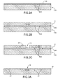
- Steps a) to g) of the process will now be described in detail.
- the method according to the invention advantageously uses a first substrate 2 made of monocrystalline silicon.
- a mask 4 is produced on the surface of the substrate 2 by deposition of a thin layer of about 100 nm.
- This layer 4 is for example silicon nitride.
- a lithography step then takes place on the layer 4 to delimit the areas of the layer 2 to be etched and an etching step of the layer 4 takes place, exposing an area 6 of the substrate 2.
- the zone 6 is made porous to a given thickness, for example by electrochemical porosification etching.
- This engraving is an engraving at the time.
- the thickness of silicon rendered porous is between 0.1 microns and 10 microns, advantageously, it is equal to about 1 micron.
- porous silicon portion is designated 8.
- porous portions are within the scope of the present invention and depends on the structure to be produced.
- the porous portion 6 has pores 6.1 of very small surface size, which improves the quality of the silicon which will grow by epitaxy on this porous portion, and larger pores 6.2 in depth, which allows selective etching or faster oxidation of the porous silicon.
- This porous portion having different pore sizes can be obtained by modifying the electrochemical etching conditions during the porosification step, for example by changing the current density.
- the desired pore size is between 2 and 50 nm, the material obtained is then of the mesoporous type.
- the mask 4 is removed, for example by chemical etching of the silicon nitride.
- step b) of epitaxial growth of a layer 10 of silicon or SiGe this layer is monocrystalline above the porous portion 6 and may be monocrystalline or polycrystalline throughout the rest of the substrate surface .
- the Silicon or Si-Ge polycrystalline can be obtained by depositing, for example, an oxide or nitride layer on the surface of the substrate before epitaxy.
- the thickness of the layer 10 is between a few tens of nm and a few tens of microns, advantageously, it is equal to about 0.25 microns.
- the layer 10 may be of semiconductor material identical to that of the first substrate or of another semiconductor material preferably having a mesh parameter close to that of the material of the first substrate.
- a first Si substrate for example an epitaxy of Si or SiGe is carried out.
- the layer 10 and the substrate 2 are separated by a dashed line.
- the element thus obtained is represented on the Figure 1B .
- the silicon portion 12 formed above the porous zone 6 will be etched to form a first suspended zone 14.
- the first suspended zone 14 is defined.
- a lithography is performed to make a mask on the surface of the layer 10 and then an etching of the portion 12 with a stop on or in the portion porous silicon 6.
- the etching is for example a deep etching by reactive ions or DRIE ("deep reactive-ion etching" in English).
- the first suspended zone 14 forms in the case of so-called M & NEMS structure the NEMS part.
- the porous portion 6 is removed or even only an oxidation thereof.
- This shrinkage can be achieved by means of wet porous silicon etching.
- This etching has the characteristic of etching the porous silicon more quickly than the "non-porous" silicon, thus by controlling the etching time, the porous silicon is removed while the suspended zone 14 has not or very little been etched.
- the duration of the engraving can be between a few seconds and a few minutes, depending on the concentration and the temperature of the etching solution used, which may be KOH, TMAH (Tetramethylammonium hydroxide), ....
- the etching lasts a few minutes in a solution of KOH at room temperature.
- the removal of the porous silicon is obtained in two steps, firstly by carrying out a thermal oxidation and then by etching the oxide formed by etching with hydrofluoric acid vapor and / or wet.
- Porous silicon oxidizes much faster than "non-porous" silicon, so by controlling the duration of the oxidation step, it is possible to oxidize virtually only porous silicon. For example, it is desired to oxidize a silicon thickness of a few tens of nm.
- the oxidation conditions are well known to those skilled in the art and will not be described in detail. According to this alternative, this etching can take place during the etching of the sacrificial layer which will be described later. The duration of the process can thus be advantageously reduced.
- a deposit 16 is made on the front face of the first substrate so as to completely or partially embed the first suspended zone 14 and to cover the front face of the first substrate.
- the material of the deposit 16 is selective with respect to the silicon, for example it is made of SiO 2 .
- the layer 16 then forms a sacrificial layer.
- This layer 16 also makes it possible to block (entirely or partially) the cavities resulting from the etching of the So porous.
- the thermal oxide around the suspended zone 14 and in the cavity forms a layer of stopping and provides increased protection during the f) machining step.
- the coating is partial or only covers the first suspended zone 14.
- a planarization step of the oxide layer 16 can take place in the case where the topology or the roughness of the surface obtained after deposition of the layer 16 is too great.
- This planarization is for example performed by chemical mechanical polishing.
- a support is then sealed or deposited on the rear face of the first substrate (step e ').
- the support is formed by a second monocrystalline silicon substrate 18 sealed on the first substrate on the front face.
- the sacrificial layer 16 is then disposed between the first substrate 2 and the second substrate 18.
- the assembly is carried out for example by direct sealing (or SDB for "Silicon Direct Bonding" in English terminology) which is a technique well known to those skilled in the art.
- direct sealing or SDB for "Silicon Direct Bonding” in English terminology
- the deposition of the support or second substrate it can be made by rolling.
- the support could be in a material different from that of the first substrate, it is even possible to consider using a glass support, for example Pyrex ® .
- This thinning makes it possible to define the thickness of the MEMS part in the case of structures called MEMS & NEMS.
- a layer of metal is deposited in order to make the electrical contacts 20, on the rear face of the first substrate 2, which forms the front face of the element obtained by sealing the first and second substrates.
- a lithography step and then an etching step are performed to form the contacts 20.
- a lithography and an engraving, of the deep-reactive ion etching (DRIE) type, for example, of the first substrate 2 are carried out so as to clear the first zone.
- the etching reaches the sacrificial layer 16 and the porous silicon if it has not been removed beforehand.
- the structuring steps of the first substrate are known steps of the MEMS & NEMS technology.
- the suspended zones 14, 17 are released for example by a wet or vapor-phase etching of the sacrificial layer 16 and porous silicon oxidized, where appropriate, with hydrofluoric acid. This is a time engraving ( figure 1H ).
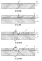
- FIGS. 2A to 2C we can see an alternative embodiment of the method for producing the Figures 1A to 1H wherein the second substrate 118 is structured prior to sealing to the first substrate.
- Such preliminary structuring can be carried out for the manufacture of CMOS circuits, in order to produce a substrate provided with electrodes, for example for exciting the active part or parts to form an electrical routing, to form one or more cavities.
- the structuring of the second substrate 118 can be done as follows:
- a photolithography step is performed to delimit the areas of the surface of the substrate to be etched and etched from the surface of the substrate to a depth of, for example, 0.5 ⁇ m.
- Engraving is an engraving with stop over time. Mechanical stops 122 are thus formed.
- a layer of SiO 2 124 is then deposited on the structured surface, this layer will form a sealing layer.
- the layer 24 is brought into contact with the sacrificial layer 16, for example by direct sealing as previously described.
- a step of thinning of the first substrate is then carried out for example by "back-grinding", which makes it possible, for example, to define the thickness of the MEMS portion in the case of a MEMS & NEMS system.
- the electrical contacts are then made in a manner similar to the method of the Figures 1A to 1H .
- the first substrate 2 is structured similarly to step f) and the suspended structures are freed by hydrofluoric acid.
- the hydrofluoric acid etches the sacrificial layer 16 and the layer 26.
- the element thus obtained is represented on the Figure 2C .
- the second substrate 118 has mechanical stops 22 downwards in the vertical direction in the representation of the Figure 2C performed prior to sealing with the first substrate.
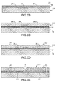
- FIGS. 3A to 3E another variant of an embodiment according to the invention can be seen in which the sacrificial layer deposited on the first substrate is structured before sealing and intermediate layers are deposited on the structured sacrificial layer before sealing.
- a lithography step takes place on the sacrificial layer 16 to delimit the zones 27 of the first layer 16 to be etched and a step of etching the layer 16 with a stop on the silicon, ie on the layer of epitaxial silicon.
- a layer of polysilicon is deposited to form, for example, a lower electrode 28.1 and an electrical route 28.2.
- a lithography step then takes place on the layer 28 and an etching step of the layer 28 takes place with a stop on the sacrificial layer 16.
- a stopping layer 30 is made, for example made of SiN which is selective with respect to the SiO 2 during the release step.
- a sealing layer 32 is deposited on the layer 30, for example made of SiO 2 .
- a planarization step of the layer 32 takes place, for example by mechanical-chemical polishing.
- the first substrate 202 thus obtained is represented on the figure 3B .
- the first substrate 202 and the second substrate 18 or 118 are sealed.
- the element thus obtained is represented on the figure 3C .
- a first thinning step of the first substrate is carried out, for example by back-grinding, followed by chemical-mechanical polishing.
- the electrical contacts 20 are then produced in a manner similar to the method of the Figures 1A to 1H .
- the first substrate 2 is structured in a manner similar to step g) and the suspended structures are released by etching the sacrificial layer 16 with hydrofluoric acid.
- the first substrate 2 before making the porous silicon portion or portions 6, for example to produce a substrate provided with an electrode, one or more electrical routes, one or more cavities ...
- the method according to the invention makes it possible to produce more than two thicknesses, by repeating steps a) to e), the intermediate sacrificial layers, ie those which do not serve as an interface layer during sealing, are then machined in defined patterns before epitaxy.
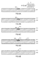
- a layer 403 of porous silicon is produced which extends over the entire surface of the substrate.
- the porous layer 403 is obtained for example by electrochemical porosification etching. This engraving is an engraving at the time.
- the thickness of silicon rendered porous is between 0.5 microns and a few tens of microns, advantageously, it is equal to about 5 microns.
- a monocrystalline silicon layer 405 is produced by epitaxial growth over the entire porous layer 403.
- This layer has, for example, a thickness of between 1 ⁇ m and a few tens of ⁇ m. The thickness of this layer defines the thickness of the MEMS portion in a MEMS & NEMS structure.
- a zone 406 made of porous silicon is produced in a manner similar to step a) of the process shown in FIGS. Figures 1A to 1H by lithography for example by means of a mask type SiN and porosification.
- a silicon layer of a semiconductor 410 is formed by epitaxy, the latter being monocrystalline on at least the porous zone 406.
- the layer 410 has a thickness of, for example, between a few hundred nm and a few tens of ⁇ m. .
- the thickness of this layer defines, for example, the thickness of the NEMS portion in a MEMS & NEMS structure.
- a lithography is carried out to delimit a first suspended structure 414 above the porous zone 406, and an etching is then performed, for example of the DRIE type, until it opens into the porous zone 406.
- element thus obtained is represented on the figure 4C .
- porous silicon is removed from zone 406 in a manner similar to the method described in connection with the Figures 1A to 1H for example by etching.
- a deposit 416 is made on the front face of the first substrate so as to completely or partially embed the first suspended zone 114 and to cover the front face of the first substrate.
- the material of the deposit 16 is selective with respect to the silicon, for example it is made of SiO 2 .
- the layer 16 then forms a sacrificial layer.
- a planarization step of the oxide layer 16 can take place in the case where the topology or the roughness of the surface obtained after deposition of the layer 16 is too great.
- This planarization is for example performed by chemical mechanical polishing.
- a support is sealed or deposited on the rear face of the first substrate.
- the support is formed by a second monocrystalline silicon substrate 118 sealed on the first substrate on the front face.
- the assembly is carried out for example by direct sealing (or SDB for "Silicon Direct Bonding" in English terminology) which is a technique well known to those skilled in the art.
- direct sealing or SDB for "Silicon Direct Bonding" in English terminology
- the deposition of the support or second substrate it can be made by rolling.
- the porous silicon layer 105 is then etched, for example by wet etching; the portion of the substrate located opposite the first element suspended relative to the porous layer 105 can then be removed. In fact, the first substrate is thinned.
- This method offers the advantage of providing good control of MEMS thickness by epitaxy.
- the variants of the production method according to the invention are not exclusive of each other and can be combined.
- the pillars have for example a width of between about 0.5 microns and 2 microns and are arranged from each other at a distance of between about 0.3 microns and 1 micron.
- a first monocrystalline silicon substrate 302 is used on which the active part will be made.
- a mask is made by photolithography on the surface of the substrate 302.
- the mask defines for example a honeycomb network as shown seen from above. on the figure 6 .
- the width of the inter-pillar zones d is, for example, between 0.3 ⁇ m and 1 ⁇ m and the distance D between two parallel faces of a pillar is for example between 0.5 ⁇ m and 2 ⁇ m.
- the width d and the distance D are represented on the Figure 5A ' .
- a step of etching the substrate 302 then takes place, for example of the DRIE type with time-out, to a depth typically between 0.5 ⁇ m and 2 ⁇ m.
- the silicon portion formed of pillars is designated by the reference 306 (detail view).
- the mask is removed.
- the layer thus formed has a thickness typically between 1 micron and a few tens of microns.
- the epitaxial layer 310 closes the zone 306.
- the epitaxial growth is carried out in a deoxidizing environment, for example under an atmosphere having a high hydrogen concentration, preferably using thrichlorosilane SiHCl 3 .
- An epitaxial layer 310 grows on the surface of the pillars and closes the cavity in which the pillars are located.
- a high-temperature annealing is carried out at a temperature close to the melting temperature of said material in the case of SiN pillars, the temperature is about 1200 ° C., which causes the pillars to collapse.
- a suspended membrane 307 is then formed above zone 306. Planarization by chemical mechanical polishing can be carried out to improve the surface condition and possibly thin the thickness of this membrane.
- the first suspended zone 314 is defined.
- a lithography is performed to make a mask on the surface of the layer 310 and then an etching of the portion 312 with a stop in the cavity.
- the etching is for example a deep etching by reactive ions or DRIE ("deep reactive-ion etching" in English).
- the first suspended zone forms, in the case of the so-called M & NEMS structure, the NEMS part ( figure 5D ).
- FIG. 6A ' represents a top view of the element of the Figure 6A .
- lithography and etching, for example by DRIE, of the epitaxial layer 510 above the abutments, is carried out.
- a first suspended structure for example the NEMS part in MEMS and NEMS technology until it opens into the cavity containing the pillars.
- the element thus formed is represented on the Figure 6C .
- a high temperature annealing step is carried out, which is sufficient to completely oxidize the pillars.
- An oxide layer 513 is also formed over the entire surface of the element.
- the NEMS portion is also oxidized, which causes during the deoxidation step a decrease in its section. This reduction in section can be anticipated by appropriately choosing the size of the NEMS etch mask and the thickness of the epitaxial layer.
- the element thus formed is represented on the Figure 6D .
- the oxide is removed by wet etching or steam for example by means of hydrofluoric acid.
- the pillars are then deleted.
- the element thus formed is represented on the figure 6E .
- This variant is particularly advantageous in the case where the pillars are sufficiently thin, for example in the case where they measure 0.6 ⁇ m side, and are spaced 0.3 microns.
- the method according to the invention it is possible not to resort to the use of SOI substrate and no longer to perform thick epitaxy. A gain in cost and time is then obtained. The duration of the process is also reduced by the fact that it is no longer necessary to carry out an important chemical mechanical polishing step after epitaxy to make up for differences in thickness between the single crystal and polycrystalline zones.
- CMOS co-integration it is also possible to perform a CMOS co-integration in three dimensions.
- the second substrate is replaced by a CMOS substrate.
- the recovery of the contacts can be done either by vias or TSV (Through-silcon via English terminology), or during sealing, by a eutectic in this case, AIGe type for example, which are well known techniques of skilled person.
- the method according to the invention is particularly suitable for producing microelectromechanical sensors and actuators and / or nanoelectromechanical systems.
Applications Claiming Priority (1)
| Application Number | Priority Date | Filing Date | Title |
|---|---|---|---|
| FR1160972A FR2983188B1 (fr) | 2011-11-30 | 2011-11-30 | Procede de realisation d'une structure comportant au moins une partie active multiepaisseur |
Publications (2)
| Publication Number | Publication Date |
|---|---|
| EP2599746A1 true EP2599746A1 (de) | 2013-06-05 |
| EP2599746B1 EP2599746B1 (de) | 2018-12-19 |
Family
ID=47221249
Family Applications (1)
| Application Number | Title | Priority Date | Filing Date |
|---|---|---|---|
| EP12194881.4A Active EP2599746B1 (de) | 2011-11-30 | 2012-11-29 | Verfahren zur Herstellung einer Struktur mit mindestens einem aus mehreren Dicken bestehenden aktiven Teil |
Country Status (4)
| Country | Link |
|---|---|
| US (1) | US8716052B2 (de) |
| EP (1) | EP2599746B1 (de) |
| JP (1) | JP6108793B2 (de) |
| FR (1) | FR2983188B1 (de) |
Cited By (6)
| Publication number | Priority date | Publication date | Assignee | Title |
|---|---|---|---|---|
| EP2952472A2 (de) | 2014-06-05 | 2015-12-09 | Commissariat à l'Énergie Atomique et aux Énergies Alternatives | Verbessertes herstellungsverfahren von hängeelementen unterschiedlicher dicke für mems- und nems-struktur |
| CN105439074A (zh) * | 2015-12-24 | 2016-03-30 | 杭州士兰微电子股份有限公司 | 空腔薄膜及其制造方法 |
| CN105502278A (zh) * | 2015-12-24 | 2016-04-20 | 杭州士兰微电子股份有限公司 | 空腔薄膜及其制造方法 |
| EP3216754A1 (de) | 2016-03-07 | 2017-09-13 | Soitec | Struktur für eine vorrichtung mit integrierten mikroelektromechanischen systemen |
| EP3257808A1 (de) * | 2016-06-17 | 2017-12-20 | Commissariat à l'énergie atomique et aux énergies alternatives | Mikroelektromechanische und/oder nanoelektromechanische vorrichtung mit bewegung ausserhalb der ebene, die mit kapazitiven mitteln zur änderung der oberfläche ausgestattet ist |
| US10315916B2 (en) | 2017-06-16 | 2019-06-11 | Commissariat A L'energie Atomique Et Aux Energies Alternatives | Microelectromechanical device with at least one translationally guided moveable element |
Families Citing this family (5)
| Publication number | Priority date | Publication date | Assignee | Title |
|---|---|---|---|---|
| US7109092B2 (en) * | 2003-05-19 | 2006-09-19 | Ziptronix, Inc. | Method of room temperature covalent bonding |
| FR3002219B1 (fr) * | 2013-02-19 | 2015-04-10 | Commissariat Energie Atomique | Procede de fabrication d'une structure micromecanique et/ou nanomecanique comportant une surface poreuse |
| CN104282547B (zh) * | 2014-06-17 | 2019-06-11 | 上海华虹宏力半导体制造有限公司 | 麦克风mems减薄工艺方法 |
| CN109399553A (zh) * | 2017-08-15 | 2019-03-01 | 无锡华润上华科技有限公司 | 一种半导体器件的制备方法 |
| JP7420369B2 (ja) * | 2019-10-21 | 2024-01-23 | 学校法人立命館 | 定量化方法、演算装置、及び、コンピュータプログラム |
Citations (3)
| Publication number | Priority date | Publication date | Assignee | Title |
|---|---|---|---|---|
| US20040065931A1 (en) * | 2000-12-22 | 2004-04-08 | Hubert Benzel | Method for producing a semiconductor component having a movable mass in particular, and semiconductor component produced according to this method |
| DE102006007729A1 (de) * | 2006-02-20 | 2007-08-23 | Robert Bosch Gmbh | Verfahren zur Herstellung eines MEMS-Substrats, entsprechendes MEMS-Substrat und MEMS-Prozess unter Verwendung des MEMS-Substrats |
| US20110147864A1 (en) * | 2008-06-10 | 2011-06-23 | Torsten Kramer | Method for manufacturing a micromechanical diaphragm structure having access from the rear of the substrate |
Family Cites Families (6)
| Publication number | Priority date | Publication date | Assignee | Title |
|---|---|---|---|---|
| EP1544163B1 (de) | 2003-12-16 | 2021-02-24 | Robert Bosch GmbH | Verfahren zur Herstellung eines Membransensors und entsprechender Membransensor |
| JP4347867B2 (ja) | 2006-07-27 | 2009-10-21 | 株式会社日立製作所 | めっき付着量制御システムおよびめっき付着量制御方法 |
| DE102008001185A1 (de) * | 2008-04-15 | 2009-10-29 | Robert Bosch Gmbh | Verfahren zur Herstellung einer mikromechanischen Membranstruktur mit feststehendem Gegenelement |
| FR2932788A1 (fr) * | 2008-06-23 | 2009-12-25 | Commissariat Energie Atomique | Procede de fabrication d'un composant electromecanique mems / nems. |
| FR2933683B1 (fr) * | 2008-07-09 | 2010-09-03 | Commissariat Energie Atomique | Structure mems/nens comportant un ancrage partiellement monocristallin et son procede de fabrication |
| FR2957339B1 (fr) * | 2010-03-10 | 2012-03-16 | Commissariat Energie Atomique | Procede de fabrication d'un microsysteme electromecanique |
-
2011
- 2011-11-30 FR FR1160972A patent/FR2983188B1/fr not_active Expired - Fee Related
-
2012
- 2012-11-29 JP JP2012260857A patent/JP6108793B2/ja not_active Expired - Fee Related
- 2012-11-29 US US13/688,746 patent/US8716052B2/en active Active
- 2012-11-29 EP EP12194881.4A patent/EP2599746B1/de active Active
Patent Citations (3)
| Publication number | Priority date | Publication date | Assignee | Title |
|---|---|---|---|---|
| US20040065931A1 (en) * | 2000-12-22 | 2004-04-08 | Hubert Benzel | Method for producing a semiconductor component having a movable mass in particular, and semiconductor component produced according to this method |
| DE102006007729A1 (de) * | 2006-02-20 | 2007-08-23 | Robert Bosch Gmbh | Verfahren zur Herstellung eines MEMS-Substrats, entsprechendes MEMS-Substrat und MEMS-Prozess unter Verwendung des MEMS-Substrats |
| US20110147864A1 (en) * | 2008-06-10 | 2011-06-23 | Torsten Kramer | Method for manufacturing a micromechanical diaphragm structure having access from the rear of the substrate |
Non-Patent Citations (2)
| Title |
|---|
| PH. ROBERT ET AL: "M&NEMS: A new approach for ultra-low cost 3D inertial sensor", 2009 IEEE SENSORS, 1 October 2009 (2009-10-01), pages 963 - 966, XP055023740, ISBN: 978-1-42-444548-6, DOI: 10.1109/ICSENS.2009.5398195 * |
| PH. ROBERT; V. NGUYEN; S. HENTZ; L. DURAFFOURG; G. JOURDAN; J. ARCAMONE; S. HARRISSON; M&NEMS: "A new approach for ultra-low cost 3D inertial sensor", IEEE SENSORS 2009 CONFERENCE, 25 October 2009 (2009-10-25) |
Cited By (12)
| Publication number | Priority date | Publication date | Assignee | Title |
|---|---|---|---|---|
| EP2952472A2 (de) | 2014-06-05 | 2015-12-09 | Commissariat à l'Énergie Atomique et aux Énergies Alternatives | Verbessertes herstellungsverfahren von hängeelementen unterschiedlicher dicke für mems- und nems-struktur |
| US9802817B2 (en) | 2014-06-05 | 2017-10-31 | Commissariat à l'énergie atomique et aux énergies alternatives | Method for making suspended elements with different thicknesses for a MEMS and NEMS structure |
| CN105439074A (zh) * | 2015-12-24 | 2016-03-30 | 杭州士兰微电子股份有限公司 | 空腔薄膜及其制造方法 |
| CN105502278A (zh) * | 2015-12-24 | 2016-04-20 | 杭州士兰微电子股份有限公司 | 空腔薄膜及其制造方法 |
| CN105439074B (zh) * | 2015-12-24 | 2017-06-16 | 杭州士兰微电子股份有限公司 | 空腔薄膜及其制造方法 |
| CN105502278B (zh) * | 2015-12-24 | 2017-11-24 | 杭州士兰微电子股份有限公司 | 空腔薄膜及其制造方法 |
| EP3216754A1 (de) | 2016-03-07 | 2017-09-13 | Soitec | Struktur für eine vorrichtung mit integrierten mikroelektromechanischen systemen |
| US10343902B2 (en) | 2016-03-07 | 2019-07-09 | Soitec | Structure for device with integrated microelectromechanical systems |
| EP3257808A1 (de) * | 2016-06-17 | 2017-12-20 | Commissariat à l'énergie atomique et aux énergies alternatives | Mikroelektromechanische und/oder nanoelektromechanische vorrichtung mit bewegung ausserhalb der ebene, die mit kapazitiven mitteln zur änderung der oberfläche ausgestattet ist |
| FR3052765A1 (fr) * | 2016-06-17 | 2017-12-22 | Commissariat Energie Atomique | Dispositif microelectromecanique et/ou nanoelectromecanique a deplacement hors-plan comportant des moyens capacitifs a variation de surface |
| US11156459B2 (en) | 2016-06-17 | 2021-10-26 | Commissariat A L'energie Atomique Et Aux Energies Alternatives | Microelectromechanical or/and nanoelectromechanical device with out-of-plane displacement having capacitive elements having a variable surface |
| US10315916B2 (en) | 2017-06-16 | 2019-06-11 | Commissariat A L'energie Atomique Et Aux Energies Alternatives | Microelectromechanical device with at least one translationally guided moveable element |
Also Published As
| Publication number | Publication date |
|---|---|
| US8716052B2 (en) | 2014-05-06 |
| FR2983188A1 (fr) | 2013-05-31 |
| US20130137245A1 (en) | 2013-05-30 |
| FR2983188B1 (fr) | 2016-07-01 |
| JP6108793B2 (ja) | 2017-04-05 |
| JP2013111746A (ja) | 2013-06-10 |
| EP2599746B1 (de) | 2018-12-19 |
Similar Documents
| Publication | Publication Date | Title |
|---|---|---|
| EP2599746B1 (de) | Verfahren zur Herstellung einer Struktur mit mindestens einem aus mehreren Dicken bestehenden aktiven Teil | |
| EP2143684B1 (de) | Herstellungsverfahren von einer MEMS-/NEMS-Struktur die eine teilweise monokristalline Verankerung besitzt | |
| EP2075222B1 (de) | Method of manufacturing mechanical components of MEMS or NEMS structures in monocrystalline silicon | |
| EP2138451B1 (de) | Verfahren zur Herstellung eines elektromechanischen MEMS-Bauteils in einem einkristallinen Material | |
| EP2138454B1 (de) | Herstellungsverfahren für ein Bauteil ausgehend von einem Substrat mit einer Opferschicht aus einkristallinem Silizium | |
| EP2599745B1 (de) | Verfahren zum Herstellen eines MEMS Bauteil mit bewegliche Teile unterschiedlicher Dicke | |
| EP1834924A2 (de) | Einkapselung in einem hermetisch abgeschlossenen Hohlraum einer mikroelektronischen Verbindung, insbesondere eines MEMS | |
| FR2863603A1 (fr) | Procede de fabrication d'un composant semi-conducteur et composant obtenu, notamment capteur a membrane | |
| EP2808297B1 (de) | Verfahren zur Herstellung eines frei hängenden Teils einer mikro- und/oder nanoelektronischen Struktur in einem monolithischen Teil eines Substrats | |
| EP2952472B1 (de) | Verbessertes herstellungsverfahren von hängeelementen unterschiedlicher dicke für mems- und nems-struktur | |
| FR2969664A1 (fr) | Procede de clivage d'un substrat | |
| WO2012028518A1 (fr) | Procédé de réalisation d'un film, par exemple monocristallin, sur un support en polymère | |
| EP3900064B1 (de) | Verfahren zum übertragen einer oberflächenschicht auf hohlräume | |
| EP2138453B1 (de) | Verfahren zur Herstellung einer elektromechanischen Struktur, die mindestens eine Stütze zur mechanischen Verstärkung umfasst | |
| EP2543625B1 (de) | Verfahren zur Herstellung eines eingebetteten Metallteils in einer Uhr | |
| EP2862836B1 (de) | Elektrochemisches Herstellungsverfahren mindestens einer porösen Zone einer mikro- und/oder nanoelektrischen Struktur | |
| EP1133684B1 (de) | Mikromechanische struktur mit einer deformierbaren membran und verfahren zu ihrer herstellung | |
| EP1263675A1 (de) | Schwebende dreidimensionale mikrointegrierte struktur und herstellungsverfahren | |
| EP2404868A1 (de) | Herstellungsverfahren einer festen Struktur eines bestimmten Volumens, in die ein mobiles Element, insbesondere ein MEMS, eingefügt werden soll | |
| FR2953819A1 (fr) | Procede de fabrication d'un composant electronique associant un systeme electromecanique et un circuit electronique. | |
| WO2002076881A1 (fr) | Procede de fabrication d'une structure a membrane micro-usinee | |
| FR2883275A1 (fr) | Composant micromecanique et procede de fabrication | |
| FR3108439A1 (fr) | Procede de fabrication d’une structure empilee | |
| FR3111628A1 (fr) | Procédé de fabrication d’un dispositif microélectronique comprenant une membrane suspendue au-dessus d’une cavité | |
| FR3048425A1 (fr) | Structure pour dispositif avec microsystemes electromecaniques integres |
Legal Events
| Date | Code | Title | Description |
|---|---|---|---|
| PUAI | Public reference made under article 153(3) epc to a published international application that has entered the european phase |
Free format text: ORIGINAL CODE: 0009012 |
|
| AK | Designated contracting states |
Kind code of ref document: A1 Designated state(s): AL AT BE BG CH CY CZ DE DK EE ES FI FR GB GR HR HU IE IS IT LI LT LU LV MC MK MT NL NO PL PT RO RS SE SI SK SM TR |
|
| AX | Request for extension of the european patent |
Extension state: BA ME |
|
| 17P | Request for examination filed |
Effective date: 20131204 |
|
| RBV | Designated contracting states (corrected) |
Designated state(s): AL AT BE BG CH CY CZ DE DK EE ES FI FR GB GR HR HU IE IS IT LI LT LU LV MC MK MT NL NO PL PT RO RS SE SI SK SM TR |
|
| STAA | Information on the status of an ep patent application or granted ep patent |
Free format text: STATUS: EXAMINATION IS IN PROGRESS |
|
| 17Q | First examination report despatched |
Effective date: 20171212 |
|
| GRAP | Despatch of communication of intention to grant a patent |
Free format text: ORIGINAL CODE: EPIDOSNIGR1 |
|
| STAA | Information on the status of an ep patent application or granted ep patent |
Free format text: STATUS: GRANT OF PATENT IS INTENDED |
|
| INTG | Intention to grant announced |
Effective date: 20180711 |
|
| GRAS | Grant fee paid |
Free format text: ORIGINAL CODE: EPIDOSNIGR3 |
|
| GRAA | (expected) grant |
Free format text: ORIGINAL CODE: 0009210 |
|
| STAA | Information on the status of an ep patent application or granted ep patent |
Free format text: STATUS: THE PATENT HAS BEEN GRANTED |
|
| AK | Designated contracting states |
Kind code of ref document: B1 Designated state(s): AL AT BE BG CH CY CZ DE DK EE ES FI FR GB GR HR HU IE IS IT LI LT LU LV MC MK MT NL NO PL PT RO RS SE SI SK SM TR |
|
| REG | Reference to a national code |
Ref country code: GB Ref legal event code: FG4D Free format text: NOT ENGLISH |
|
| REG | Reference to a national code |
Ref country code: CH Ref legal event code: EP |
|
| REG | Reference to a national code |
Ref country code: IE Ref legal event code: FG4D Free format text: LANGUAGE OF EP DOCUMENT: FRENCH |
|
| REG | Reference to a national code |
Ref country code: DE Ref legal event code: R096 Ref document number: 602012054809 Country of ref document: DE |
|
| REG | Reference to a national code |
Ref country code: AT Ref legal event code: REF Ref document number: 1078481 Country of ref document: AT Kind code of ref document: T Effective date: 20190115 |
|
| REG | Reference to a national code |
Ref country code: NL Ref legal event code: MP Effective date: 20181219 |
|
| PG25 | Lapsed in a contracting state [announced via postgrant information from national office to epo] |
Ref country code: LV Free format text: LAPSE BECAUSE OF FAILURE TO SUBMIT A TRANSLATION OF THE DESCRIPTION OR TO PAY THE FEE WITHIN THE PRESCRIBED TIME-LIMIT Effective date: 20181219 Ref country code: FI Free format text: LAPSE BECAUSE OF FAILURE TO SUBMIT A TRANSLATION OF THE DESCRIPTION OR TO PAY THE FEE WITHIN THE PRESCRIBED TIME-LIMIT Effective date: 20181219 Ref country code: BG Free format text: LAPSE BECAUSE OF FAILURE TO SUBMIT A TRANSLATION OF THE DESCRIPTION OR TO PAY THE FEE WITHIN THE PRESCRIBED TIME-LIMIT Effective date: 20190319 Ref country code: NO Free format text: LAPSE BECAUSE OF FAILURE TO SUBMIT A TRANSLATION OF THE DESCRIPTION OR TO PAY THE FEE WITHIN THE PRESCRIBED TIME-LIMIT Effective date: 20190319 Ref country code: HR Free format text: LAPSE BECAUSE OF FAILURE TO SUBMIT A TRANSLATION OF THE DESCRIPTION OR TO PAY THE FEE WITHIN THE PRESCRIBED TIME-LIMIT Effective date: 20181219 Ref country code: LT Free format text: LAPSE BECAUSE OF FAILURE TO SUBMIT A TRANSLATION OF THE DESCRIPTION OR TO PAY THE FEE WITHIN THE PRESCRIBED TIME-LIMIT Effective date: 20181219 |
|
| REG | Reference to a national code |
Ref country code: LT Ref legal event code: MG4D |
|
| REG | Reference to a national code |
Ref country code: AT Ref legal event code: MK05 Ref document number: 1078481 Country of ref document: AT Kind code of ref document: T Effective date: 20181219 |
|
| PG25 | Lapsed in a contracting state [announced via postgrant information from national office to epo] |
Ref country code: SE Free format text: LAPSE BECAUSE OF FAILURE TO SUBMIT A TRANSLATION OF THE DESCRIPTION OR TO PAY THE FEE WITHIN THE PRESCRIBED TIME-LIMIT Effective date: 20181219 Ref country code: GR Free format text: LAPSE BECAUSE OF FAILURE TO SUBMIT A TRANSLATION OF THE DESCRIPTION OR TO PAY THE FEE WITHIN THE PRESCRIBED TIME-LIMIT Effective date: 20190320 Ref country code: AL Free format text: LAPSE BECAUSE OF FAILURE TO SUBMIT A TRANSLATION OF THE DESCRIPTION OR TO PAY THE FEE WITHIN THE PRESCRIBED TIME-LIMIT Effective date: 20181219 Ref country code: RS Free format text: LAPSE BECAUSE OF FAILURE TO SUBMIT A TRANSLATION OF THE DESCRIPTION OR TO PAY THE FEE WITHIN THE PRESCRIBED TIME-LIMIT Effective date: 20181219 |
|
| PG25 | Lapsed in a contracting state [announced via postgrant information from national office to epo] |
Ref country code: NL Free format text: LAPSE BECAUSE OF FAILURE TO SUBMIT A TRANSLATION OF THE DESCRIPTION OR TO PAY THE FEE WITHIN THE PRESCRIBED TIME-LIMIT Effective date: 20181219 |
|
| PG25 | Lapsed in a contracting state [announced via postgrant information from national office to epo] |
Ref country code: PT Free format text: LAPSE BECAUSE OF FAILURE TO SUBMIT A TRANSLATION OF THE DESCRIPTION OR TO PAY THE FEE WITHIN THE PRESCRIBED TIME-LIMIT Effective date: 20190419 Ref country code: CZ Free format text: LAPSE BECAUSE OF FAILURE TO SUBMIT A TRANSLATION OF THE DESCRIPTION OR TO PAY THE FEE WITHIN THE PRESCRIBED TIME-LIMIT Effective date: 20181219 Ref country code: ES Free format text: LAPSE BECAUSE OF FAILURE TO SUBMIT A TRANSLATION OF THE DESCRIPTION OR TO PAY THE FEE WITHIN THE PRESCRIBED TIME-LIMIT Effective date: 20181219 Ref country code: PL Free format text: LAPSE BECAUSE OF FAILURE TO SUBMIT A TRANSLATION OF THE DESCRIPTION OR TO PAY THE FEE WITHIN THE PRESCRIBED TIME-LIMIT Effective date: 20181219 Ref country code: IT Free format text: LAPSE BECAUSE OF FAILURE TO SUBMIT A TRANSLATION OF THE DESCRIPTION OR TO PAY THE FEE WITHIN THE PRESCRIBED TIME-LIMIT Effective date: 20181219 |
|
| PG25 | Lapsed in a contracting state [announced via postgrant information from national office to epo] |
Ref country code: IS Free format text: LAPSE BECAUSE OF FAILURE TO SUBMIT A TRANSLATION OF THE DESCRIPTION OR TO PAY THE FEE WITHIN THE PRESCRIBED TIME-LIMIT Effective date: 20190419 Ref country code: RO Free format text: LAPSE BECAUSE OF FAILURE TO SUBMIT A TRANSLATION OF THE DESCRIPTION OR TO PAY THE FEE WITHIN THE PRESCRIBED TIME-LIMIT Effective date: 20181219 Ref country code: SK Free format text: LAPSE BECAUSE OF FAILURE TO SUBMIT A TRANSLATION OF THE DESCRIPTION OR TO PAY THE FEE WITHIN THE PRESCRIBED TIME-LIMIT Effective date: 20181219 Ref country code: EE Free format text: LAPSE BECAUSE OF FAILURE TO SUBMIT A TRANSLATION OF THE DESCRIPTION OR TO PAY THE FEE WITHIN THE PRESCRIBED TIME-LIMIT Effective date: 20181219 Ref country code: SM Free format text: LAPSE BECAUSE OF FAILURE TO SUBMIT A TRANSLATION OF THE DESCRIPTION OR TO PAY THE FEE WITHIN THE PRESCRIBED TIME-LIMIT Effective date: 20181219 |
|
| REG | Reference to a national code |
Ref country code: DE Ref legal event code: R097 Ref document number: 602012054809 Country of ref document: DE |
|
| PLBE | No opposition filed within time limit |
Free format text: ORIGINAL CODE: 0009261 |
|
| STAA | Information on the status of an ep patent application or granted ep patent |
Free format text: STATUS: NO OPPOSITION FILED WITHIN TIME LIMIT |
|
| PG25 | Lapsed in a contracting state [announced via postgrant information from national office to epo] |
Ref country code: AT Free format text: LAPSE BECAUSE OF FAILURE TO SUBMIT A TRANSLATION OF THE DESCRIPTION OR TO PAY THE FEE WITHIN THE PRESCRIBED TIME-LIMIT Effective date: 20181219 Ref country code: DK Free format text: LAPSE BECAUSE OF FAILURE TO SUBMIT A TRANSLATION OF THE DESCRIPTION OR TO PAY THE FEE WITHIN THE PRESCRIBED TIME-LIMIT Effective date: 20181219 |
|
| 26N | No opposition filed |
Effective date: 20190920 |
|
| PG25 | Lapsed in a contracting state [announced via postgrant information from national office to epo] |
Ref country code: SI Free format text: LAPSE BECAUSE OF FAILURE TO SUBMIT A TRANSLATION OF THE DESCRIPTION OR TO PAY THE FEE WITHIN THE PRESCRIBED TIME-LIMIT Effective date: 20181219 |
|
| PG25 | Lapsed in a contracting state [announced via postgrant information from national office to epo] |
Ref country code: TR Free format text: LAPSE BECAUSE OF FAILURE TO SUBMIT A TRANSLATION OF THE DESCRIPTION OR TO PAY THE FEE WITHIN THE PRESCRIBED TIME-LIMIT Effective date: 20181219 |
|
| REG | Reference to a national code |
Ref country code: CH Ref legal event code: PL |
|
| PG25 | Lapsed in a contracting state [announced via postgrant information from national office to epo] |
Ref country code: MC Free format text: LAPSE BECAUSE OF FAILURE TO SUBMIT A TRANSLATION OF THE DESCRIPTION OR TO PAY THE FEE WITHIN THE PRESCRIBED TIME-LIMIT Effective date: 20181219 Ref country code: LI Free format text: LAPSE BECAUSE OF NON-PAYMENT OF DUE FEES Effective date: 20191130 Ref country code: CH Free format text: LAPSE BECAUSE OF NON-PAYMENT OF DUE FEES Effective date: 20191130 Ref country code: LU Free format text: LAPSE BECAUSE OF NON-PAYMENT OF DUE FEES Effective date: 20191129 |
|
| REG | Reference to a national code |
Ref country code: BE Ref legal event code: MM Effective date: 20191130 |
|
| PG25 | Lapsed in a contracting state [announced via postgrant information from national office to epo] |
Ref country code: IE Free format text: LAPSE BECAUSE OF NON-PAYMENT OF DUE FEES Effective date: 20191129 |
|
| PG25 | Lapsed in a contracting state [announced via postgrant information from national office to epo] |
Ref country code: BE Free format text: LAPSE BECAUSE OF NON-PAYMENT OF DUE FEES Effective date: 20191130 |
|
| PG25 | Lapsed in a contracting state [announced via postgrant information from national office to epo] |
Ref country code: CY Free format text: LAPSE BECAUSE OF FAILURE TO SUBMIT A TRANSLATION OF THE DESCRIPTION OR TO PAY THE FEE WITHIN THE PRESCRIBED TIME-LIMIT Effective date: 20181219 |
|
| PG25 | Lapsed in a contracting state [announced via postgrant information from national office to epo] |
Ref country code: HU Free format text: LAPSE BECAUSE OF FAILURE TO SUBMIT A TRANSLATION OF THE DESCRIPTION OR TO PAY THE FEE WITHIN THE PRESCRIBED TIME-LIMIT; INVALID AB INITIO Effective date: 20121129 Ref country code: MT Free format text: LAPSE BECAUSE OF FAILURE TO SUBMIT A TRANSLATION OF THE DESCRIPTION OR TO PAY THE FEE WITHIN THE PRESCRIBED TIME-LIMIT Effective date: 20181219 |
|
| PG25 | Lapsed in a contracting state [announced via postgrant information from national office to epo] |
Ref country code: MK Free format text: LAPSE BECAUSE OF FAILURE TO SUBMIT A TRANSLATION OF THE DESCRIPTION OR TO PAY THE FEE WITHIN THE PRESCRIBED TIME-LIMIT Effective date: 20181219 |
|
| PGFP | Annual fee paid to national office [announced via postgrant information from national office to epo] |
Ref country code: GB Payment date: 20221123 Year of fee payment: 11 Ref country code: FR Payment date: 20221118 Year of fee payment: 11 Ref country code: DE Payment date: 20221121 Year of fee payment: 11 |