EP2597860A1 - Image capture device, endoscope, and manufacturing method of image capture device - Google Patents
Image capture device, endoscope, and manufacturing method of image capture device Download PDFInfo
- Publication number
- EP2597860A1 EP2597860A1 EP11809500.9A EP11809500A EP2597860A1 EP 2597860 A1 EP2597860 A1 EP 2597860A1 EP 11809500 A EP11809500 A EP 11809500A EP 2597860 A1 EP2597860 A1 EP 2597860A1
- Authority
- EP
- European Patent Office
- Prior art keywords
- image pickup
- pickup apparatus
- pickup device
- principal surface
- optical path
- Prior art date
- Legal status (The legal status is an assumption and is not a legal conclusion. Google has not performed a legal analysis and makes no representation as to the accuracy of the status listed.)
- Granted
Links
Images



Classifications
-
- H—ELECTRICITY
- H10—SEMICONDUCTOR DEVICES; ELECTRIC SOLID-STATE DEVICES NOT OTHERWISE PROVIDED FOR
- H10F—INORGANIC SEMICONDUCTOR DEVICES SENSITIVE TO INFRARED RADIATION, LIGHT, ELECTROMAGNETIC RADIATION OF SHORTER WAVELENGTH OR CORPUSCULAR RADIATION
- H10F77/00—Constructional details of devices covered by this subclass
- H10F77/40—Optical elements or arrangements
- H10F77/413—Optical elements or arrangements directly associated or integrated with the devices, e.g. back reflectors
-
- A—HUMAN NECESSITIES
- A61—MEDICAL OR VETERINARY SCIENCE; HYGIENE
- A61B—DIAGNOSIS; SURGERY; IDENTIFICATION
- A61B1/00—Instruments for performing medical examinations of the interior of cavities or tubes of the body by visual or photographical inspection, e.g. endoscopes; Illuminating arrangements therefor
- A61B1/00064—Constructional details of the endoscope body
- A61B1/00071—Insertion part of the endoscope body
- A61B1/0008—Insertion part of the endoscope body characterised by distal tip features
- A61B1/00096—Optical elements
-
- A—HUMAN NECESSITIES
- A61—MEDICAL OR VETERINARY SCIENCE; HYGIENE
- A61B—DIAGNOSIS; SURGERY; IDENTIFICATION
- A61B1/00—Instruments for performing medical examinations of the interior of cavities or tubes of the body by visual or photographical inspection, e.g. endoscopes; Illuminating arrangements therefor
- A61B1/04—Instruments for performing medical examinations of the interior of cavities or tubes of the body by visual or photographical inspection, e.g. endoscopes; Illuminating arrangements therefor combined with photographic or television appliances
- A61B1/05—Instruments for performing medical examinations of the interior of cavities or tubes of the body by visual or photographical inspection, e.g. endoscopes; Illuminating arrangements therefor combined with photographic or television appliances characterised by the image sensor, e.g. camera, being in the distal end portion
-
- A—HUMAN NECESSITIES
- A61—MEDICAL OR VETERINARY SCIENCE; HYGIENE
- A61B—DIAGNOSIS; SURGERY; IDENTIFICATION
- A61B1/00—Instruments for performing medical examinations of the interior of cavities or tubes of the body by visual or photographical inspection, e.g. endoscopes; Illuminating arrangements therefor
- A61B1/04—Instruments for performing medical examinations of the interior of cavities or tubes of the body by visual or photographical inspection, e.g. endoscopes; Illuminating arrangements therefor combined with photographic or television appliances
- A61B1/05—Instruments for performing medical examinations of the interior of cavities or tubes of the body by visual or photographical inspection, e.g. endoscopes; Illuminating arrangements therefor combined with photographic or television appliances characterised by the image sensor, e.g. camera, being in the distal end portion
- A61B1/051—Details of CCD assembly
-
- H—ELECTRICITY
- H04—ELECTRIC COMMUNICATION TECHNIQUE
- H04N—PICTORIAL COMMUNICATION, e.g. TELEVISION
- H04N23/00—Cameras or camera modules comprising electronic image sensors; Control thereof
- H04N23/50—Constructional details
- H04N23/555—Constructional details for picking-up images in sites, inaccessible due to their dimensions or hazardous conditions, e.g. endoscopes or borescopes
-
- H—ELECTRICITY
- H04—ELECTRIC COMMUNICATION TECHNIQUE
- H04N—PICTORIAL COMMUNICATION, e.g. TELEVISION
- H04N7/00—Television systems
- H04N7/18—Closed-circuit television [CCTV] systems, i.e. systems in which the video signal is not broadcast
- H04N7/183—Closed-circuit television [CCTV] systems, i.e. systems in which the video signal is not broadcast for receiving images from a single remote source
-
- H—ELECTRICITY
- H10—SEMICONDUCTOR DEVICES; ELECTRIC SOLID-STATE DEVICES NOT OTHERWISE PROVIDED FOR
- H10F—INORGANIC SEMICONDUCTOR DEVICES SENSITIVE TO INFRARED RADIATION, LIGHT, ELECTROMAGNETIC RADIATION OF SHORTER WAVELENGTH OR CORPUSCULAR RADIATION
- H10F39/00—Integrated devices, or assemblies of multiple devices, comprising at least one element covered by group H10F30/00, e.g. radiation detectors comprising photodiode arrays
- H10F39/011—Manufacture or treatment of image sensors covered by group H10F39/12
- H10F39/024—Manufacture or treatment of image sensors covered by group H10F39/12 of coatings or optical elements
-
- H—ELECTRICITY
- H10—SEMICONDUCTOR DEVICES; ELECTRIC SOLID-STATE DEVICES NOT OTHERWISE PROVIDED FOR
- H10F—INORGANIC SEMICONDUCTOR DEVICES SENSITIVE TO INFRARED RADIATION, LIGHT, ELECTROMAGNETIC RADIATION OF SHORTER WAVELENGTH OR CORPUSCULAR RADIATION
- H10F39/00—Integrated devices, or assemblies of multiple devices, comprising at least one element covered by group H10F30/00, e.g. radiation detectors comprising photodiode arrays
- H10F39/011—Manufacture or treatment of image sensors covered by group H10F39/12
- H10F39/026—Wafer-level processing
-
- H—ELECTRICITY
- H10—SEMICONDUCTOR DEVICES; ELECTRIC SOLID-STATE DEVICES NOT OTHERWISE PROVIDED FOR
- H10F—INORGANIC SEMICONDUCTOR DEVICES SENSITIVE TO INFRARED RADIATION, LIGHT, ELECTROMAGNETIC RADIATION OF SHORTER WAVELENGTH OR CORPUSCULAR RADIATION
- H10F39/00—Integrated devices, or assemblies of multiple devices, comprising at least one element covered by group H10F30/00, e.g. radiation detectors comprising photodiode arrays
- H10F39/80—Constructional details of image sensors
- H10F39/804—Containers or encapsulations
-
- H—ELECTRICITY
- H10—SEMICONDUCTOR DEVICES; ELECTRIC SOLID-STATE DEVICES NOT OTHERWISE PROVIDED FOR
- H10F—INORGANIC SEMICONDUCTOR DEVICES SENSITIVE TO INFRARED RADIATION, LIGHT, ELECTROMAGNETIC RADIATION OF SHORTER WAVELENGTH OR CORPUSCULAR RADIATION
- H10F39/00—Integrated devices, or assemblies of multiple devices, comprising at least one element covered by group H10F30/00, e.g. radiation detectors comprising photodiode arrays
- H10F39/80—Constructional details of image sensors
- H10F39/806—Optical elements or arrangements associated with the image sensors
-
- H—ELECTRICITY
- H10—SEMICONDUCTOR DEVICES; ELECTRIC SOLID-STATE DEVICES NOT OTHERWISE PROVIDED FOR
- H10F—INORGANIC SEMICONDUCTOR DEVICES SENSITIVE TO INFRARED RADIATION, LIGHT, ELECTROMAGNETIC RADIATION OF SHORTER WAVELENGTH OR CORPUSCULAR RADIATION
- H10F71/00—Manufacture or treatment of devices covered by this subclass
-
- H—ELECTRICITY
- H10—SEMICONDUCTOR DEVICES; ELECTRIC SOLID-STATE DEVICES NOT OTHERWISE PROVIDED FOR
- H10F—INORGANIC SEMICONDUCTOR DEVICES SENSITIVE TO INFRARED RADIATION, LIGHT, ELECTROMAGNETIC RADIATION OF SHORTER WAVELENGTH OR CORPUSCULAR RADIATION
- H10F77/00—Constructional details of devices covered by this subclass
- H10F77/40—Optical elements or arrangements
- H10F77/407—Optical elements or arrangements indirectly associated with the devices
Definitions
- the present invention relates to an image pickup apparatus, an endoscope and an image pickup apparatus manufacturing method, and specifically relates to an image pickup apparatus manufactured by wafer-level chip-size packaging, an endoscope including the image pickup apparatus and a method for manufacturing the image pickup apparatus.
- An image pickup apparatus includes an image pickup device substrate portion with a solid-state image pickup device formed thereon, and a cover glass portion that protects the solid-state image pickup device.
- Image pickup apparatus manufacturing methods using wafer-level chip-size packaging (WL-CSP) for downsizing and mass production of image pickup apparatuses are known.
- WL-CSP wafer-level chip-size packaging
- Japanese Patent Application Laid-Open Publication No. 2003-204053 discloses a method in which a semiconductor wafer with a large number of image pickup devices formed thereon and, e.g., a glass substrate are bonded and the resulting semiconductor wafer is subsequently cut for singulation to obtain a large number of image pickup apparatuses in a batch.
- Japanese Patent Application Laid-Open Publication No. 2002-45333 discloses a horizontal image pickup apparatus that shoots an object in a direction perpendicular to an image pickup device surface.
- a step of bonding a right angle prism to an upper face of a cover glass is necessary.
- An object of the present invention is to provide a small-size image pickup apparatus, an endoscope including a small-size image pickup apparatus and a method for manufacturing a small-size image pickup apparatus.
- An image pickup apparatus includes: a transparent substrate portion including an optical path conversion element function portion; an image pickup device substrate portion including an image pickup device on a first principal surface and a back-face electrode on a second principal surface, the back-face electrode being connected to the image pickup device via a wiring portion; and a bonding layer that bonds the transparent substrate portion and the image pickup device substrate portion that have a same outer dimension.
- an endoscope includes: an image pickup optical system including a plurality of lens portions; an image pickup apparatus including a transparent substrate portion including an optical path conversion element function portion, an image pickup device substrate portion including an image pickup device on a first principal surface and a back-face electrode on a second principal surface, the back-face electrode being connected to the image pickup device via a wiring portion, and a transparent substrate portion having an outer dimension equal to an outer dimension of the image pickup device substrate portion and being bonded to the image pickup device substrate portion via a bonding layer; and a barrel portion.
- a method for manufacturing an image pickup apparatus including: an image pickup device substrate fabricating step of fabricating an image pickup device substrate including a plurality of image pickup devices on a first principal surface and a plurality of back-face electrodes on a second principal surface, the plurality of back-face electrodes being connected to the respective image pickup devices via respective wiring portions; a bonded substrate fabricating step of fabricating a bonded substrate by bonding a transparent substrate to the first principal surface of the image pickup device substrate via a bonding layer; a prism fabricating step of fabricating an optical path conversion element by forming a groove portion in the transparent substrate on the image pickup devices, the groove portion including a perpendicular surface perpendicular to the first principal surface and an inclined surface inclined relative to the first principal surface; and a singulation step of singulating the bonded substrate into individual image pickup apparatuses.
- the image pickup apparatus 1 includes an image pickup device substrate portion 10, a bonding layer 20 and a cover glass portion 30, which is a transparent substrate portion.
- the image pickup apparatus 1 is of a horizontal type, and a light beam incident on a perpendicular surface 32 of the cover glass portion 30 from the left side in the diagram in Fig. 1 is reflected by an inclined surface 31 and reaches an image pickup device 13 via a lower face 33.
- the image pickup apparatus 1 is manufactured by wafer-level chip-size packaging. In other words, a large number of image pickup apparatuses are manufactured in a batch at the stage of a wafer and then the wafer is singulated into individual chips (image pickup apparatuses) by means of cutting (dicing) processing.
- outer dimensions (dimensions of a surface where an image pickup device is formed) of each of the image pickup device substrate portion 10, the bonding layer 20 and the cover glass portion 30 are outer dimensions, i.e., L1 and L2, of the image pickup apparatus 1.
- respective outer dimensions (bottom face dimensions) of the image pickup device substrate portion 10, the bonding layer 20 and the cover glass portion 30 as observed from above are the same.
- the image pickup device substrate portion 10 and the cover glass portion 30 have respective side faces with a same inclination angle ⁇ 1, respective outer dimensions in an L1 direction of the image pickup device substrate portion 10, the bonding layer 20 and the cover glass portion 30 are slightly different from one another to be exact. However, since the difference is slight, the respective outer dimensions of the device substrate portion 10 and the cover glass portion 30 are regarded as being the same.
- the image pickup device substrate portion 10 includes the image pickup device 13 on a first principal surface 11 and back-face electrodes 17 on a second principal surface 12, the back-face electrodes 17 being connected to the image pickup device 13 via through-wirings 16, which are wiring portions.
- the through-wirings 16 are connected to the image pickup device 13 via front-face electrodes 15 and front-face wirings (not illustrated).
- a number of microlenses 14, the number being equal to a number of pixels, are formed on an upper face of the image pickup device 13.
- the inclined surface 31 is a reflective surface of the right angle prism, and as already described, a light beam entering from the perpendicular surface 32 is reflected by the inclined surface 31, resulting in an optical path of the light beam being converted by 90 degrees, whereby the light beam enters the image pickup device 13.
- the bonding layer 20 that bonds the cover glass portion 30 to the image pickup device substrate portion 10 is provided in such a manner that an air gap 22 is formed above a region of the image pickup device substrate portion 10 where the image pickup device is formed.
- the air gap 22 is formed by the bonding layer 20 having a frame-like shape.
- the bonding layer 20 is not formed in the region where the image pickup device is formed.
- the image pickup apparatus 1 Since the image pickup apparatus 1 is manufactured by WL-CSP, a cover glass portion that protects the image pickup device 13 is essential. As already described, known horizontal image pickup apparatuses require a right angle prism to be further disposed on a cover glass portion. However, in the image pickup apparatus 1, the cover glass portion 30 has a function as a right angle prism and thus, the image pickup apparatus 1 has a small size and provides good productivity.
- the microlenses 14 formed on the image pickup device 13 highly effectively collect light.
- the image pickup device substrate 10W includes, for example, a single-crystal silicon substrate, and on the first principal surface 11, the plurality of image pickup devices 13 are formed using a semiconductor circuit fabricating technique. Note that, although e.g., CCDs or CMOSs are preferably used as the image pickup devices, separately-manufactured image pickup device chips may be disposed on the image pickup device substrate 10W. On the respective image pickup devices 13, a number of microlenses, the number being equal to a number of pixels, are formed using, for example a transparent resin.
- front-face electrodes 15 which are connected to front-face wirings (not illustrated) for power supply and signal transmission for the image pickup device 13, are formed.
- the second principal surface 12 of the image pickup device substrate 10W is subjected to, e.g., dry etching processing or wet etching processing to form through-holes that reach back faces of the respective front-face electrodes 15.
- the through-holes are formed as via holes that extend through the single-crystal silicon substrate and include respective bottom portions formed by the respective front-face electrodes 15.
- a conductor such as copper or aluminum is provided in respective inner portions and the bottom portions of the through-holes to form through-wirings 16, which are electrically connected to the respective front-face electrodes 15. Furthermore, back-face electrodes 17 connected to the respective through-wirings 16 are formed on the second principal surface 12.
- the back-face electrodes 17 are external connection electrodes for mounting, and are formed using, e.g., projecting copper bumps or solder balls.
- FIG. 3 indicates an example in which image pickup devices 13 are arranged in a grid of 6x6 on the image pickup device substrate 10W, in reality, image pickup devices 13 are arranged in a grid of 10 ⁇ 10 or more, and preferably in a grid of 20x20 or more.
- a glass substrate 30W which is a transparent substrate, is bonded to the first principal surface 11 of the image pickup device substrate 10W via a bonding layer 20W to fabricate a bonded substrate 1 W.
- an antireflective film may be formed on a lower face 33 of the glass substrate 30W.
- the bonding layer 20W is formed as a result of application of an adhesive bond in a pattern using, e.g., screen printing or ink-jetting.
- the adhesive bond is not applied to regions of the first principal surface 11 of the image pickup device substrate 10W where the image pickup devices are formed.
- the adhesive bond applied to regions in the peripheries of the image pickup devices except the regions where the image pickup devices are formed are subjected to curing processing after the lower face 33 of the glass substrate 30W are bonded to the adhesive bond.
- an ultraviolet curable resin or a thermosetting resin may be used for the adhesive bond.
- air gap 22 is a sealed space
- a surface of the blade 2 where no bevel is formed is kept to have an angle of 90 degrees relative to the first principal surface 11 during the dicing processing.
- the inclined surfaces 31 that serve as reflective surfaces of prisms and the perpendicular surfaces 32 that serve as light incident surfaces of the prisms are simultaneously formed.
- FIG. 5 indicates a blade including a straight cutting part for ease of illustration, it should be understood that normally, a circular blade, which is widely used in general, may be used.
- the bonded substrate 1W is divided into rod-like substrates 1V each including a plurality of image pickup devices via the groove portions 3.
- bottom portions of the groove portions 3 reach the second principal surface 12 of the image pickup device substrate 10W.
- the grinding processing is performed. This is because it is difficult to provide a flatness and a surface roughness acceptable for image pickup optical systems by the dicing processing using the blade 2 only.
- the grinding processing is performed until flat surfaces meeting optical specifications are provided, by a method using, e.g., a grinding solution that is similar to those used in normal prism grinding.
- the grinding processing is performed with reference to the second principal surface 12 on which the back-face electrodes 17 of the image pickup apparatuses 1 are formed, and an angle and a distance (plate thickness) between the first principal surface 11 and the second principal surface 12 are managed with high precision.
- the grinding processing may be performed for each of the image pickup apparatuses after a singulation step, which will be described later, as illustrated in Fig. 8 , it is preferable that the grinding processing be performed at the stage of the rod-like substrates 1V each including a row of image pickup apparatuses 1.
- the grinding processing of the rod-like substrates 1V is time-efficient and highly productive because processing of a plurality of image pickup apparatuses in a row is performed in a batch, and in addition, enables precisions in processing of prisms in the plurality of image pickup apparatuses to be managed to be even.
- the rod-like substrate 1V is singulated into individual image pickup apparatuses 1.
- the manufacturing method according to the present embodiment enables effective manufacturing of small-size image pickup apparatuses 1. In other words, the manufacturing method according to the present embodiment provides high productivity.
- an image pickup apparatus 1A according to a second embodiment of the present invention and a method for manufacturing the image pickup apparatus 1A will be described.
- the image pickup apparatus 1A according to the present embodiment and the method for manufacturing the image pickup apparatus 1A are similar to the image pickup apparatus 1 according to the first embodiment and the method for manufacturing the image pickup apparatus 1, and thus, components that are the same as those of the first embodiment are provided with reference numerals that are the same as those of the first embodiment and a description thereof will be omitted.
- a bonding layer 20A in the image pickup apparatus 1A As illustrated in Fig. 9 , no air gap is formed in a bonding layer 20A in the image pickup apparatus 1A. This is because an image pickup device includes no microlens. Thus, the bonding layer 20A is easy to fabricate compared to the bonding layer 20 that requires patterning.
- the image pickup apparatus 1A includes a reflective film 35 including a metal thin film on an inclined surface 31.
- the reflective film 35 enhances a reflection efficiency of the reflective surface of the prism. Provision of the reflective film 35 on the reflective surface of the prism enables observation of a bright image.
- the reflective film 35 is formed by, e.g., vapor deposition or sputtering using a metal film with high reflectivity such as aluminum or silver.
- a protection film including, e.g., SiO 2 outside the reflective film 35, for prevention of oxidation of the metal film. From the perspective of productivity, it is preferable that the reflective film 35 and the protection film be formed at the stage of rod-like substrates 1V.
- the inclined surface 31 having the reflective film 35 thereon provides enhanced light reflection efficiency.
- the image pickup apparatus 1A efficiently forms an image of a light beam from an image pickup optical system on an image pickup device 13 because of smaller reflection loss at the inclined surface 31.
- rod-like substrates 1V are fabricated by a step-cut method.
- a blade 2 forms grooves only in a glass substrate 30W.
- bottom portions of the grooves do not reach an image pickup device substrate.
- a bonded substrate 1W is not separated into rod-like substrates 1V and remains in a state of a wafer in which the groove portions 3 are formed.
- the bonded substrate 1 W is separated into rod-like substrates 1V. Note that side faces of an image pickup device substrate portion 10A are perpendicular to the first principal surface 11.
- a V-shaped groove including two reflective surfaces are formed using a blade with opposite surfaces each having an inclination of 45 degrees; and a bottom portion of the V-shaped groove and a separation part between two rod-like substrates are separated by a perpendicular surface, respectively.
- a chip size L1 of the image pickup apparatus 1A is set to be substantially equal to a height H1 of the prism, that is, a thickness of a cover glass portion 30.
- a prism is not disposed on the cover glass portion 30 but a prism is fabricated by processing the cover glass portion 30, enabling fabrication of a prism with a requisite minimum size.
- the prism in each of the image pickup apparatuses 1 and 1A includes an upper face 34.
- This is intended to facilitate handling of the rod-like substrates 1V and the image pickup apparatuses 1 and 1A.
- the image pickup apparatus 1 including the upper face 34 when the image pickup apparatus 1 is mounted on a wiring board, the mounting can be performed with reference to the upper face 34 parallel to the lower face 33, that is, the first principal surface 11.
- the image pickup apparatus 1 having the above-described structure is resistant to, e.g., chipping compared to a case where the image pickup apparatus 1 includes an acute-angled glass end face.
- FIG. 10 is a diagram illustrating a cross-sectional structure of a distal end portion of an insertion portion of the endoscope 40.
- an image pickup optical system 43 including a plurality of lens portions 41 and an image pickup apparatus 1A are fixed by a barrel portion 46.
- the inside of the barrel portion 46 is charged with a non-conducive resin filler having high thermal conductivity.
- a cable 45 is connected to a wiring board 44 on which the image pickup apparatus 1A is mounted via back-face electrodes 17.
- the image pickup optical system 43 is fixed after alignment (optical position adjustment).
- an optical path of an optical image from the image pickup optical system 43 is converted by 90 degrees by an inclined surface 31, whereby the optical image is formed on a pixel area of the image pickup device 13.
- the cover glass portion 30, which is essential as a protective member is a right angle prism having an optical path conversion function, and thus, the endoscope 40 enables reduction in diameter and is less invasive. Furthermore, the endoscope 40 is low in cost because of the high productivity.
- the reflective film described in the second embodiment may be used in the image pickup apparatus 1 according to the first embodiment, or the image pickup apparatus 1 according to the first embodiment may be installed in the endoscope according to the third embodiment.
Landscapes
- Health & Medical Sciences (AREA)
- Life Sciences & Earth Sciences (AREA)
- Surgery (AREA)
- Engineering & Computer Science (AREA)
- Nuclear Medicine, Radiotherapy & Molecular Imaging (AREA)
- Medical Informatics (AREA)
- Veterinary Medicine (AREA)
- Biophysics (AREA)
- Biomedical Technology (AREA)
- Optics & Photonics (AREA)
- Pathology (AREA)
- Radiology & Medical Imaging (AREA)
- Public Health (AREA)
- Molecular Biology (AREA)
- Heart & Thoracic Surgery (AREA)
- General Health & Medical Sciences (AREA)
- Physics & Mathematics (AREA)
- Animal Behavior & Ethology (AREA)
- Signal Processing (AREA)
- Multimedia (AREA)
- Solid State Image Pick-Up Elements (AREA)
- Instruments For Viewing The Inside Of Hollow Bodies (AREA)
- Studio Devices (AREA)
- Endoscopes (AREA)
- Manufacturing & Machinery (AREA)
- Transforming Light Signals Into Electric Signals (AREA)
Abstract
Description
- The present invention relates to an image pickup apparatus, an endoscope and an image pickup apparatus manufacturing method, and specifically relates to an image pickup apparatus manufactured by wafer-level chip-size packaging, an endoscope including the image pickup apparatus and a method for manufacturing the image pickup apparatus.
- Electronic endoscopes, camera-equipped mobile phones and digital cameras, etc., that include an image pickup apparatus including a solid-state image pickup device such as a CCD or a CMOS have widely been used. An image pickup apparatus includes an image pickup device substrate portion with a solid-state image pickup device formed thereon, and a cover glass portion that protects the solid-state image pickup device.
- Image pickup apparatus manufacturing methods using wafer-level chip-size packaging (WL-CSP) for downsizing and mass production of image pickup apparatuses are known. For example, Japanese Patent Application Laid-Open Publication No.
2003-204053 - Also, Japanese Patent Application Laid-Open Publication No.
2002-45333 - In other words, since known horizontal image pickup apparatuses require a step of bonding a prism to each of image pickup apparatuses obtained as a result of singulation after the image pickup apparatuses are manufactured in a batch by WL-CSP, the productivity is sometimes not good. Furthermore, for image pickup apparatuses obtained by WL-CSP, a cover glass is essential for protecting an image pickup device. However, a dimension in a height direction (direction perpendicular to an image pickup element surface) of an image pickup apparatus is increased by the amount of a thickness of the cover glass. Thus, where a horizontal image pickup apparatus manufactured by WL-CSP is mounted in a distal end of an endoscope, the size of the distal end of the endoscope may be increased.
- An object of the present invention is to provide a small-size image pickup apparatus, an endoscope including a small-size image pickup apparatus and a method for manufacturing a small-size image pickup apparatus.
- An image pickup apparatus according to an embodiment of the present invention includes: a transparent substrate portion including an optical path conversion element function portion; an image pickup device substrate portion including an image pickup device on a first principal surface and a back-face electrode on a second principal surface, the back-face electrode being connected to the image pickup device via a wiring portion; and a bonding layer that bonds the transparent substrate portion and the image pickup device substrate portion that have a same outer dimension.
- Also, an endoscope according to another embodiment of the present invention includes: an image pickup optical system including a plurality of lens portions; an image pickup apparatus including a transparent substrate portion including an optical path conversion element function portion, an image pickup device substrate portion including an image pickup device on a first principal surface and a back-face electrode on a second principal surface, the back-face electrode being connected to the image pickup device via a wiring portion, and a transparent substrate portion having an outer dimension equal to an outer dimension of the image pickup device substrate portion and being bonded to the image pickup device substrate portion via a bonding layer; and a barrel portion.
- Also, a method for manufacturing an image pickup apparatus according to still another embodiment of the present invention, the method including: an image pickup device substrate fabricating step of fabricating an image pickup device substrate including a plurality of image pickup devices on a first principal surface and a plurality of back-face electrodes on a second principal surface, the plurality of back-face electrodes being connected to the respective image pickup devices via respective wiring portions; a bonded substrate fabricating step of fabricating a bonded substrate by bonding a transparent substrate to the first principal surface of the image pickup device substrate via a bonding layer; a prism fabricating step of fabricating an optical path conversion element by forming a groove portion in the transparent substrate on the image pickup devices, the groove portion including a perpendicular surface perpendicular to the first principal surface and an inclined surface inclined relative to the first principal surface; and a singulation step of singulating the bonded substrate into individual image pickup apparatuses.
-
-
Fig. 1 is an outer appearance diagram of an image pickup apparatus according to a first embodiment; -
Fig. 2 is an exploded view of the image pickup apparatus according to the first embodiment; -
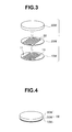
Fig. 3 is a diagram illustrating a bonded substrate fabricating step for the image pickup apparatus according to the first embodiment; -
Fig. 4 is an outer appearance diagram illustrating a bonded substrate of the image pickup apparatus according to the first embodiment; -
Fig. 5 is a perspective diagram illustrating a prism fabricating step for the image pickup apparatus according to the first embodiment; -
Fig. 6 is a cross-sectional structural diagram illustrating the prism fabricating step for the image pickup apparatus according to the first embodiment; -
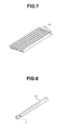
Fig. 7 is a perspective diagram illustrating the prism fabricating step for the image pickup apparatus according to the first embodiment; -
Fig. 8 is a perspective diagram illustrating a singulation step for the image pickup apparatus according to the first embodiment; -
Fig. 9 is a cross-sectional structural diagram illustrating an image pickup apparatus according to a second embodiment; and -
Fig. 10 is a cross-sectional structural diagram illustrating an endoscope including an image pickup apparatus according to a third embodiment. - An
image pickup apparatus 1 according to a first embodiment of the present invention and a method for manufacturing theimage pickup apparatus 1 will be described below with reference to the drawings. First, a structure of theimage pickup apparatus 1 according to the present embodiment will be described. As illustrated inFigs. 1 and 2 , theimage pickup apparatus 1 includes an image pickupdevice substrate portion 10, abonding layer 20 and acover glass portion 30, which is a transparent substrate portion. Theimage pickup apparatus 1 is of a horizontal type, and a light beam incident on aperpendicular surface 32 of thecover glass portion 30 from the left side in the diagram inFig. 1 is reflected by aninclined surface 31 and reaches animage pickup device 13 via alower face 33. - As described later, the
image pickup apparatus 1 is manufactured by wafer-level chip-size packaging. In other words, a large number of image pickup apparatuses are manufactured in a batch at the stage of a wafer and then the wafer is singulated into individual chips (image pickup apparatuses) by means of cutting (dicing) processing. Thus, as illustrated inFig. 1 , outer dimensions (dimensions of a surface where an image pickup device is formed) of each of the image pickupdevice substrate portion 10, thebonding layer 20 and thecover glass portion 30 are outer dimensions, i.e., L1 and L2, of theimage pickup apparatus 1. In other words, respective outer dimensions (bottom face dimensions) of the image pickupdevice substrate portion 10, thebonding layer 20 and thecover glass portion 30 as observed from above are the same. Note that since in theimage pickup apparatus 1, the image pickupdevice substrate portion 10 and thecover glass portion 30 have respective side faces with a same inclination angle θ1, respective outer dimensions in an L1 direction of the image pickupdevice substrate portion 10, thebonding layer 20 and thecover glass portion 30 are slightly different from one another to be exact. However, since the difference is slight, the respective outer dimensions of thedevice substrate portion 10 and thecover glass portion 30 are regarded as being the same. - The image pickup
device substrate portion 10 includes theimage pickup device 13 on a firstprincipal surface 11 and back-face electrodes 17 on a secondprincipal surface 12, the back-face electrodes 17 being connected to theimage pickup device 13 via through-wirings 16, which are wiring portions. The through-wirings 16 are connected to theimage pickup device 13 via front-face electrodes 15 and front-face wirings (not illustrated). On an upper face of theimage pickup device 13, a number ofmicrolenses 14, the number being equal to a number of pixels, are formed. - The
cover glass portion 30 has a protection member function that protects theimage pickup device 13. Furthermore, in theimage pickup apparatus 1, thecover glass portion 30 includes theperpendicular surface 32 perpendicular to the firstprincipal surface 11 of the image pickupdevice substrate portion 10 and aninclined surface 31 inclined by 45 degrees relative to the firstprincipal surface 11 of the image pickupdevice substrate portion 10, and is an optical path conversion element function portion that converts a path of incident light and makes the light exit in a direction different from an incident direction. In other words, inFig. 1 , θ1 = 45 degrees and 02 = 90 degrees, and thecover glass portion 30 provides a right angle prism. Theinclined surface 31 is a reflective surface of the right angle prism, and as already described, a light beam entering from theperpendicular surface 32 is reflected by theinclined surface 31, resulting in an optical path of the light beam being converted by 90 degrees, whereby the light beam enters theimage pickup device 13. - Furthermore, the
bonding layer 20 that bonds thecover glass portion 30 to the image pickupdevice substrate portion 10 is provided in such a manner that anair gap 22 is formed above a region of the image pickupdevice substrate portion 10 where the image pickup device is formed. In other words, between the region of the image pickupdevice substrate portion 10 where the image pickup device is formed and thecover glass portion 30, theair gap 22 is formed by thebonding layer 20 having a frame-like shape. In other words, thebonding layer 20 is not formed in the region where the image pickup device is formed. - Since the
image pickup apparatus 1 is manufactured by WL-CSP, a cover glass portion that protects theimage pickup device 13 is essential. As already described, known horizontal image pickup apparatuses require a right angle prism to be further disposed on a cover glass portion. However, in theimage pickup apparatus 1, thecover glass portion 30 has a function as a right angle prism and thus, theimage pickup apparatus 1 has a small size and provides good productivity. - Furthermore, in the
image pickup apparatus 1 including theair gap 22, themicrolenses 14 formed on theimage pickup device 13 highly effectively collect light. - Next, a method for manufacturing the
image pickup apparatus 1 will be described with reference toFigs. 3 to 8 . - An image
pickup device substrate 10W including a plurality ofimage pickup devices 13 on a firstprincipal surface 11 and a plurality of back-face electrodes 17 on a secondprincipal surface 12, the plurality of back-face electrodes 17 being connected to the respectiveimage pickup devices 13 via respective through-wirings 16, is fabricated. - The image
pickup device substrate 10W includes, for example, a single-crystal silicon substrate, and on the firstprincipal surface 11, the plurality ofimage pickup devices 13 are formed using a semiconductor circuit fabricating technique. Note that, although e.g., CCDs or CMOSs are preferably used as the image pickup devices, separately-manufactured image pickup device chips may be disposed on the imagepickup device substrate 10W. On the respectiveimage pickup devices 13, a number of microlenses, the number being equal to a number of pixels, are formed using, for example a transparent resin. - On the first
principal surface 11 of the imagepickup device substrate 10W, front-face electrodes 15, which are connected to front-face wirings (not illustrated) for power supply and signal transmission for theimage pickup device 13, are formed. Then, the secondprincipal surface 12 of the imagepickup device substrate 10W is subjected to, e.g., dry etching processing or wet etching processing to form through-holes that reach back faces of the respective front-face electrodes 15. In other words, the through-holes are formed as via holes that extend through the single-crystal silicon substrate and include respective bottom portions formed by the respective front-face electrodes 15. - A conductor such as copper or aluminum is provided in respective inner portions and the bottom portions of the through-holes to form through-
wirings 16, which are electrically connected to the respective front-face electrodes 15. Furthermore, back-face electrodes 17 connected to the respective through-wirings 16 are formed on the secondprincipal surface 12. The back-face electrodes 17 are external connection electrodes for mounting, and are formed using, e.g., projecting copper bumps or solder balls. - Note that for the wiring portions connecting the
image pickup device 13 of the firstprincipal surface 11 and the back-face electrodes 17 of the secondprincipal surface 12, side-face wirings may be used instead of the through-wirings 16. - Note that although
Fig. 3 indicates an example in whichimage pickup devices 13 are arranged in a grid of 6x6 on the imagepickup device substrate 10W, in reality,image pickup devices 13 are arranged in a grid of 10×10 or more, and preferably in a grid of 20x20 or more. - As illustrated in
Figs. 3 and 4 , aglass substrate 30W, which is a transparent substrate, is bonded to the firstprincipal surface 11 of the imagepickup device substrate 10W via abonding layer 20W to fabricate a bondedsubstrate 1 W. Note that an antireflective film may be formed on alower face 33 of theglass substrate 30W. - The
bonding layer 20W is formed as a result of application of an adhesive bond in a pattern using, e.g., screen printing or ink-jetting. In other words, the adhesive bond is not applied to regions of the firstprincipal surface 11 of the imagepickup device substrate 10W where the image pickup devices are formed. The adhesive bond applied to regions in the peripheries of the image pickup devices except the regions where the image pickup devices are formed are subjected to curing processing after thelower face 33 of theglass substrate 30W are bonded to the adhesive bond. For the adhesive bond, an ultraviolet curable resin or a thermosetting resin may be used. - Note that although where the bonded substrate fabricating step is performed in a vacuum, no air exist in the
air gap 22, which is a sealed space, the term "air gap" is used for convenience. - As illustrated in
Figs. 5 and 6 , anupper face 34 of theglass substrate 30W on the image pickup devices is subjected to dicing processing using ablade 2 with a bevel of 45 degrees (θ1 = 45 degrees) on one side to formgroove portions 3 each including aperpendicular surface 32 perpendicular to the firstprincipal surface 11 and aninclined surface 31 inclined relative to the firstprincipal surface 11. In other words, a surface of theblade 2 where no bevel is formed is kept to have an angle of 90 degrees relative to the firstprincipal surface 11 during the dicing processing. As a result of the formation of thegroove portions 3 using theblade 2, theinclined surfaces 31 that serve as reflective surfaces of prisms and theperpendicular surfaces 32 that serve as light incident surfaces of the prisms are simultaneously formed. - Although
Fig. 5 indicates a blade including a straight cutting part for ease of illustration, it should be understood that normally, a circular blade, which is widely used in general, may be used. - Note that as illustrated in
Fig. 7 , in the method for manufacturing theimage pickup apparatus 1 according to the present embodiment, in the prism fabricating step, simultaneously with the prism fabrication, the bondedsubstrate 1W is divided into rod-like substrates 1V each including a plurality of image pickup devices via thegroove portions 3. In other words, bottom portions of thegroove portions 3 reach the secondprincipal surface 12 of the imagepickup device substrate 10W. - After the prism fabricating step, grinding processing of the
inclined surfaces 31 of the bondedsubstrate 1W, which serve as the reflective surfaces of the prisms, and theperpendicular surfaces 32 of the bondedsubstrate 1W, which serve as the incident surfaces, is performed. This is because it is difficult to provide a flatness and a surface roughness acceptable for image pickup optical systems by the dicing processing using theblade 2 only. The grinding processing is performed until flat surfaces meeting optical specifications are provided, by a method using, e.g., a grinding solution that is similar to those used in normal prism grinding. The grinding processing is performed with reference to the secondprincipal surface 12 on which the back-face electrodes 17 of theimage pickup apparatuses 1 are formed, and an angle and a distance (plate thickness) between the firstprincipal surface 11 and the secondprincipal surface 12 are managed with high precision. - Although the grinding processing may be performed for each of the image pickup apparatuses after a singulation step, which will be described later, as illustrated in
Fig. 8 , it is preferable that the grinding processing be performed at the stage of the rod-like substrates 1V each including a row ofimage pickup apparatuses 1. The grinding processing of the rod-like substrates 1V is time-efficient and highly productive because processing of a plurality of image pickup apparatuses in a row is performed in a batch, and in addition, enables precisions in processing of prisms in the plurality of image pickup apparatuses to be managed to be even. - As illustrated in
Fig. 8 , in a singulation step, the rod-like substrate 1V is singulated into individualimage pickup apparatuses 1. - The manufacturing method according to the present embodiment enables effective manufacturing of small-size
image pickup apparatuses 1. In other words, the manufacturing method according to the present embodiment provides high productivity. - Next, an
image pickup apparatus 1A according to a second embodiment of the present invention and a method for manufacturing theimage pickup apparatus 1A will be described. Theimage pickup apparatus 1A according to the present embodiment and the method for manufacturing theimage pickup apparatus 1A are similar to theimage pickup apparatus 1 according to the first embodiment and the method for manufacturing theimage pickup apparatus 1, and thus, components that are the same as those of the first embodiment are provided with reference numerals that are the same as those of the first embodiment and a description thereof will be omitted. - As illustrated in
Fig. 9 , no air gap is formed in abonding layer 20A in theimage pickup apparatus 1A. This is because an image pickup device includes no microlens. Thus, thebonding layer 20A is easy to fabricate compared to thebonding layer 20 that requires patterning. - Furthermore, the
image pickup apparatus 1A includes areflective film 35 including a metal thin film on aninclined surface 31. Thereflective film 35 enhances a reflection efficiency of the reflective surface of the prism. Provision of thereflective film 35 on the reflective surface of the prism enables observation of a bright image. Thereflective film 35 is formed by, e.g., vapor deposition or sputtering using a metal film with high reflectivity such as aluminum or silver. Furthermore, it is preferable to form a protection film including, e.g., SiO2 outside thereflective film 35, for prevention of oxidation of the metal film. From the perspective of productivity, it is preferable that thereflective film 35 and the protection film be formed at the stage of rod-like substrates 1V. - The
inclined surface 31 having thereflective film 35 thereon provides enhanced light reflection efficiency. In other words, theimage pickup apparatus 1A efficiently forms an image of a light beam from an image pickup optical system on animage pickup device 13 because of smaller reflection loss at theinclined surface 31. - In the case of the
image pickup apparatus 1A, rod-like substrates 1V are fabricated by a step-cut method. In other words, in a prism fabricating step, ablade 2 forms grooves only in aglass substrate 30W. In other words, bottom portions of the grooves do not reach an image pickup device substrate. Thus, after the prism fabricating step, a bondedsubstrate 1W is not separated into rod-like substrates 1V and remains in a state of a wafer in which thegroove portions 3 are formed. Then, by means of dicing processing in a separation step after the prism fabricating step, the bondedsubstrate 1 W is separated into rod-like substrates 1V. Note that side faces of an image pickupdevice substrate portion 10A are perpendicular to the firstprincipal surface 11. - Also, it is possible that: first, a V-shaped groove including two reflective surfaces are formed using a blade with opposite surfaces each having an inclination of 45 degrees; and a bottom portion of the V-shaped groove and a separation part between two rod-like substrates are separated by a perpendicular surface, respectively.
- Note that as illustrated in
Fig. 9 , as with theimage pickup apparatus 1, a chip size L1 of theimage pickup apparatus 1A is set to be substantially equal to a height H1 of the prism, that is, a thickness of acover glass portion 30. In other words, in the case of theimage pickup apparatuses cover glass portion 30 but a prism is fabricated by processing thecover glass portion 30, enabling fabrication of a prism with a requisite minimum size. - Note that as illustrated in, e.g.,
Fig. 1 , in the case of theimage pickup apparatuses glass substrate 30W are not subjected to the processing for providing the inclined surfaces 31. In other words, the prism in each of theimage pickup apparatuses upper face 34. This is intended to facilitate handling of the rod-like substrates 1V and theimage pickup apparatuses image pickup apparatus 1 including theupper face 34, when theimage pickup apparatus 1 is mounted on a wiring board, the mounting can be performed with reference to theupper face 34 parallel to thelower face 33, that is, the firstprincipal surface 11. Furthermore, theimage pickup apparatus 1 having the above-described structure is resistant to, e.g., chipping compared to a case where theimage pickup apparatus 1 includes an acute-angled glass end face. - Next, an
endoscope 40 including theimage pickup apparatus 1A will be described as a third embodiment.Fig. 10 is a diagram illustrating a cross-sectional structure of a distal end portion of an insertion portion of theendoscope 40. As illustrated inFig. 10 , in theendoscope 40 with theimage pickup apparatus 1A incorporated in the distal end portion of the insertion portion, an image pickupoptical system 43 including a plurality oflens portions 41 and animage pickup apparatus 1A are fixed by abarrel portion 46. The inside of thebarrel portion 46 is charged with a non-conducive resin filler having high thermal conductivity. Acable 45 is connected to awiring board 44 on which theimage pickup apparatus 1A is mounted via back-face electrodes 17. - Anterior to a
cover glass portion 30, which provides a prism in theimage pickup apparatus 1, the image pickupoptical system 43 is fixed after alignment (optical position adjustment). Thus, an optical path of an optical image from the image pickupoptical system 43 is converted by 90 degrees by aninclined surface 31, whereby the optical image is formed on a pixel area of theimage pickup device 13. - In the
endoscope 40 including, e.g., the image pickup apparatus. 1A in the distal end portion of the insertion portion, thecover glass portion 30, which is essential as a protective member, is a right angle prism having an optical path conversion function, and thus, theendoscope 40 enables reduction in diameter and is less invasive. Furthermore, theendoscope 40 is low in cost because of the high productivity. - The present invention is not limited to the above-described embodiments and modifications and the like, and various modifications and alternation and the like are possible without departing from the spirit of the present invention. For example, the reflective film described in the second embodiment may be used in the
image pickup apparatus 1 according to the first embodiment, or theimage pickup apparatus 1 according to the first embodiment may be installed in the endoscope according to the third embodiment. - The present application claims the priority of Japanese Patent Application No.
2010-166009
Claims (16)
- An image pickup apparatus comprising:a transparent substrate portion including an optical path conversion element function portion;an image pickup device substrate portion including an image pickup device on a first principal surface and a back-face electrode on a second principal surface, the back-face electrode being connected to the image pickup device via a wiring portion; anda bonding layer that bonds the transparent substrate portion and the image pickup device substrate portion that have a same outer dimension.
- The image pickup apparatus according to claim 1, wherein the transparent substrate portion includes a perpendicular surface perpendicular to the first principal surface and an inclined surface inclined relative to the first principal surface, and the inclined surface includes a reflective surface of the optical path conversion element function portion.
- The image pickup apparatus according to claim 2, wherein the optical path conversion element function portion includes a right angle prism, the inclined surface of which is inclined by 45 degrees relative to the first principal surface.
- The image pickup apparatus according to claim 3, wherein the image pickup apparatus is manufactured by wafer-level chip-size packaging.
- The image pickup apparatus according to claim 4, wherein a reflective film is provided on the inclined surface.
- An endoscope comprising:an image pickup optical system including a plurality of lens portions;an image pickup apparatus including a transparent substrate portion including an optical path conversion element function portion, an image pickup device substrate portion including an image pickup device on a first principal surface and a back-face electrode on a second principal surface, the back-face electrode being connected to the image pickup device via a wiring portion, and a transparent substrate portion having an outer dimension equal to an outer dimension of the image pickup device substrate portion and being bonded to the image pickup device substrate portion via a bonding layer; anda barrel portion.
- The endoscope according to claim 6, wherein the transparent substrate portion includes a perpendicular surface perpendicular to the first principal surface and an inclined surface inclined relative to the first principal surface, and the inclined surface includes a reflective surface of the optical path conversion element function portion.
- The endoscope according to claim 7, wherein the optical path conversion element function portion includes a right angle prism, the inclined surface of which is inclined by 45 degrees relative to the first principal surface.
- The endoscope according to claim 8, wherein the image pickup apparatus is manufactured by wafer-level chip-size packaging.
- The endoscope according to claim 9, wherein a reflective film is provided on the inclined surface.
- A method for manufacturing an image pickup apparatus, the method comprising:an image pickup device substrate fabricating step of fabricating an image pickup device substrate including a plurality of image pickup devices on a first principal surface and a plurality of back-face electrodes on a second principal surface, the plurality of back-face electrodes being connected to the respective image pickup devices via respective wiring portions;a bonded substrate fabricating step of fabricating a bonded substrate by bonding a transparent substrate to the first principal surface of the image pickup device substrate via a bonding layer;a prism fabricating step of fabricating an optical path conversion element by forming a groove portion in the transparent substrate on the image pickup devices, the groove portion including a perpendicular surface perpendicular to the first principal surface and an inclined surface inclined relative to the first principal surface; anda singulation step of singulating the bonded substrate into individual image pickup apparatuses.
- The method for manufacturing an image pickup apparatus according to claim 11, wherein the optical path conversion element includes a right angle prism, the inclined surface of which is inclined by 45 degrees relative to the first principal surface.
- The method for manufacturing an image pickup apparatus according to claim 12, wherein the prism fabricating step serves as a division step of dicing the bonded substrate via the groove portion into rod-like substrates each including a plurality of image pickup devices.
- The method for manufacturing an image pickup apparatus according to claim 13, further comprising a grinding step of grinding the inclined surface and the perpendicular surface of the optical path conversion element.
- The method for manufacturing an image pickup apparatus according to claim 14, wherein the bonded substrate fabricating step includes bonding each of regions in peripheries of the image pickup devices to the transparent substrate via the bonding layer to form an air gap between each of regions where the image pickup devices are formed and the transparent substrate.
- The method for manufacturing an image pickup apparatus according to claim 15, further comprising a reflective film forming step of forming a reflective film on the inclined surface.
Applications Claiming Priority (2)
| Application Number | Priority Date | Filing Date | Title |
|---|---|---|---|
| JP2010166009A JP5701532B2 (en) | 2010-07-23 | 2010-07-23 | Manufacturing method of imaging apparatus |
| PCT/JP2011/062956 WO2012011326A1 (en) | 2010-07-23 | 2011-06-06 | Image capture device, endoscope, and manufacturing method of image capture device |
Publications (3)
| Publication Number | Publication Date |
|---|---|
| EP2597860A1 true EP2597860A1 (en) | 2013-05-29 |
| EP2597860A4 EP2597860A4 (en) | 2014-07-30 |
| EP2597860B1 EP2597860B1 (en) | 2017-04-12 |
Family
ID=45496755
Family Applications (1)
| Application Number | Title | Priority Date | Filing Date |
|---|---|---|---|
| EP11809500.9A Active EP2597860B1 (en) | 2010-07-23 | 2011-06-06 | Image capture device, endoscope, and manufacturing method of image capture device |
Country Status (4)
| Country | Link |
|---|---|
| US (1) | US9281423B2 (en) |
| EP (1) | EP2597860B1 (en) |
| JP (1) | JP5701532B2 (en) |
| WO (1) | WO2012011326A1 (en) |
Cited By (1)
| Publication number | Priority date | Publication date | Assignee | Title |
|---|---|---|---|---|
| WO2017077051A1 (en) * | 2015-11-06 | 2017-05-11 | Ams Ag | Optical package and method of producing an optical package |
Families Citing this family (13)
| Publication number | Priority date | Publication date | Assignee | Title |
|---|---|---|---|---|
| CA2941578A1 (en) | 2010-09-08 | 2012-03-15 | Covidien Lp | Catheter with imaging assembly |
| EP3150106B1 (en) * | 2011-12-29 | 2024-03-27 | Cook Medical Technologies LLC | Space-optimized visualization catheter having a camera train holder in a catheter with off-centered lumens |
| JP5941753B2 (en) * | 2012-05-28 | 2016-06-29 | 富士フイルム株式会社 | Electronic endoscope apparatus, imaging module, and imaging lens molding method |
| US9517184B2 (en) | 2012-09-07 | 2016-12-13 | Covidien Lp | Feeding tube with insufflation device and related methods therefor |
| USD716841S1 (en) | 2012-09-07 | 2014-11-04 | Covidien Lp | Display screen with annotate file icon |
| US9198835B2 (en) | 2012-09-07 | 2015-12-01 | Covidien Lp | Catheter with imaging assembly with placement aid and related methods therefor |
| USD717340S1 (en) | 2012-09-07 | 2014-11-11 | Covidien Lp | Display screen with enteral feeding icon |
| USD735343S1 (en) | 2012-09-07 | 2015-07-28 | Covidien Lp | Console |
| JP6157211B2 (en) * | 2013-05-16 | 2017-07-05 | オリンパス株式会社 | Manufacturing method of imaging apparatus |
| JP6435663B2 (en) * | 2014-06-30 | 2018-12-12 | 凸版印刷株式会社 | Method for manufacturing solid-state imaging device |
| TWI696244B (en) * | 2019-08-21 | 2020-06-11 | 富元精密科技股份有限公司 | Circuit arrangement structure of edge of glass substrate and manufacturing method thereof |
| TWI727813B (en) * | 2020-05-27 | 2021-05-11 | 富元精密科技股份有限公司 | Glass substrate structure of light-emitting diode |
| JP2025022671A (en) * | 2023-08-03 | 2025-02-14 | オリンパスメディカルシステムズ株式会社 | Imaging module, endoscope, and method for manufacturing imaging module |
Family Cites Families (23)
| Publication number | Priority date | Publication date | Assignee | Title |
|---|---|---|---|---|
| JPH03279908A (en) * | 1990-03-28 | 1991-12-11 | Asahi Optical Co Ltd | Tip part of sideward view type endoscope |
| JP3209345B2 (en) * | 1991-02-04 | 2001-09-17 | 大日本印刷株式会社 | Transmissive screen and mold for producing Fresnel lens sheet |
| JP3252002B2 (en) * | 1993-02-06 | 2002-01-28 | 株式会社堀場製作所 | Method for manufacturing branching / condensing element in multi-element pyroelectric detector |
| JPH08116042A (en) * | 1994-10-18 | 1996-05-07 | Olympus Optical Co Ltd | Solid-state imaging device and manufacturing method thereof |
| JP3742514B2 (en) * | 1998-10-16 | 2006-02-08 | オリンパス株式会社 | Imaging device |
| JPH11352413A (en) * | 1999-04-27 | 1999-12-24 | Olympus Optical Co Ltd | Endoscope |
| US7813789B2 (en) * | 1999-06-15 | 2010-10-12 | Given Imaging Ltd. | In-vivo imaging device, optical system and method |
| JP2002045333A (en) | 2000-08-01 | 2002-02-12 | Fuji Photo Optical Co Ltd | Endoscopic photographing device |
| US7154549B2 (en) * | 2000-12-18 | 2006-12-26 | Fuji Photo Film Co., Ltd. | Solid state image sensor having a single-layered electrode structure |
| JP2003204053A (en) | 2001-03-05 | 2003-07-18 | Canon Inc | Imaging module, method of manufacturing the imaging module, and digital camera |
| JP4443865B2 (en) * | 2002-06-24 | 2010-03-31 | 富士フイルム株式会社 | Solid-state imaging device and manufacturing method thereof |
| JP5030360B2 (en) * | 2002-12-25 | 2012-09-19 | オリンパス株式会社 | Method for manufacturing solid-state imaging device |
| US7855727B2 (en) * | 2004-09-15 | 2010-12-21 | Gyrus Acmi, Inc. | Endoscopy device supporting multiple input devices |
| US8872906B2 (en) * | 2005-01-05 | 2014-10-28 | Avantis Medical Systems, Inc. | Endoscope assembly with a polarizing filter |
| EP2463910A3 (en) * | 2005-03-25 | 2012-08-15 | Fujifilm Corporation | Manufacturing method of a solid state imaging device |
| US20090053850A1 (en) * | 2005-03-25 | 2009-02-26 | Fujifilm Corporation | Method of manufacturing solid state imaging device |
| WO2006115147A1 (en) * | 2005-04-25 | 2006-11-02 | Asahi Glass Company, Limited | Imaging lens |
| US8208047B2 (en) * | 2005-12-16 | 2012-06-26 | Thomson Licensing | Imager and imaging method for digital cinematography |
| JP2009210874A (en) * | 2008-03-05 | 2009-09-17 | Canon Inc | Imaging apparatus |
| US8823859B2 (en) * | 2008-10-08 | 2014-09-02 | Olympus Corporation | Image pickup unit, optical unit, and manufacturing method for the image pickup unit |
| JP5165524B2 (en) * | 2008-10-10 | 2013-03-21 | シャープ株式会社 | Wafer scale lens, wafer scale module, and electronic device |
| JP2010166009A (en) | 2009-01-19 | 2010-07-29 | Canon Inc | Exposure apparatus, and method of manufacturing device |
| JP6017107B2 (en) * | 2009-12-28 | 2016-10-26 | ソニー株式会社 | Image sensor, manufacturing method thereof, and sensor device |
-
2010
- 2010-07-23 JP JP2010166009A patent/JP5701532B2/en active Active
-
2011
- 2011-06-06 WO PCT/JP2011/062956 patent/WO2012011326A1/en not_active Ceased
- 2011-06-06 EP EP11809500.9A patent/EP2597860B1/en active Active
-
2013
- 2013-01-23 US US13/747,806 patent/US9281423B2/en active Active
Cited By (3)
| Publication number | Priority date | Publication date | Assignee | Title |
|---|---|---|---|---|
| WO2017077051A1 (en) * | 2015-11-06 | 2017-05-11 | Ams Ag | Optical package and method of producing an optical package |
| CN108271423A (en) * | 2015-11-06 | 2018-07-10 | ams有限公司 | Optical package and method of producing optical package |
| US10847664B2 (en) | 2015-11-06 | 2020-11-24 | Ams Ag | Optical package and method of producing an optical package |
Also Published As
| Publication number | Publication date |
|---|---|
| US20130128020A1 (en) | 2013-05-23 |
| EP2597860A4 (en) | 2014-07-30 |
| JP5701532B2 (en) | 2015-04-15 |
| WO2012011326A1 (en) | 2012-01-26 |
| EP2597860B1 (en) | 2017-04-12 |
| US9281423B2 (en) | 2016-03-08 |
| JP2012029049A (en) | 2012-02-09 |
Similar Documents
| Publication | Publication Date | Title |
|---|---|---|
| EP2597860B1 (en) | Image capture device, endoscope, and manufacturing method of image capture device | |
| US9214592B2 (en) | Method of making interposer package for CMOS image sensor | |
| US9373660B2 (en) | Method of forming a low profile image sensor package with an image sensor substrate, a support substrate and a printed circuit board | |
| US9373653B2 (en) | Stepped package for image sensor | |
| US8092734B2 (en) | Covers for microelectronic imagers and methods for wafer-level packaging of microelectronics imagers | |
| KR101420934B1 (en) | Wire bond interposer package for cmos image sensor and method of making same | |
| JP5498684B2 (en) | Semiconductor module and manufacturing method thereof | |
| WO2010086926A1 (en) | Optical device and method for manufacturing same | |
| JP6787378B2 (en) | Interposer board | |
| US20110169118A1 (en) | Optical device, method of manufacturing the same, and electronic apparatus | |
| CN102647564A (en) | Solid-state imaging device, manufacturing method thereof, and electronic device | |
| US9190443B2 (en) | Low profile image sensor | |
| JP5965984B2 (en) | Imaging device | |
| CN104051489B (en) | Little profile imaging sensor | |
| HK1201987B (en) | Low profile image sensor | |
| HK1196181A (en) | Low profile image sensor package and method | |
| HK1196181B (en) | Low profile image sensor package and method |
Legal Events
| Date | Code | Title | Description |
|---|---|---|---|
| PUAI | Public reference made under article 153(3) epc to a published international application that has entered the european phase |
Free format text: ORIGINAL CODE: 0009012 |
|
| 17P | Request for examination filed |
Effective date: 20130123 |
|
| AK | Designated contracting states |
Kind code of ref document: A1 Designated state(s): AL AT BE BG CH CY CZ DE DK EE ES FI FR GB GR HR HU IE IS IT LI LT LU LV MC MK MT NL NO PL PT RO RS SE SI SK SM TR |
|
| DAX | Request for extension of the european patent (deleted) | ||
| A4 | Supplementary search report drawn up and despatched |
Effective date: 20140626 |
|
| RIC1 | Information provided on ipc code assigned before grant |
Ipc: A61B 1/00 20060101ALI20140620BHEP Ipc: H01L 27/146 20060101ALI20140620BHEP Ipc: H04N 5/369 20110101ALI20140620BHEP Ipc: H04N 5/225 20060101AFI20140620BHEP Ipc: A61B 1/05 20060101ALI20140620BHEP |
|
| 17Q | First examination report despatched |
Effective date: 20160303 |
|
| GRAP | Despatch of communication of intention to grant a patent |
Free format text: ORIGINAL CODE: EPIDOSNIGR1 |
|
| INTG | Intention to grant announced |
Effective date: 20161013 |
|
| RAP1 | Party data changed (applicant data changed or rights of an application transferred) |
Owner name: OLYMPUS CORPORATION |
|
| GRAS | Grant fee paid |
Free format text: ORIGINAL CODE: EPIDOSNIGR3 |
|
| GRAA | (expected) grant |
Free format text: ORIGINAL CODE: 0009210 |
|
| AK | Designated contracting states |
Kind code of ref document: B1 Designated state(s): AL AT BE BG CH CY CZ DE DK EE ES FI FR GB GR HR HU IE IS IT LI LT LU LV MC MK MT NL NO PL PT RO RS SE SI SK SM TR |
|
| REG | Reference to a national code |
Ref country code: GB Ref legal event code: FG4D |
|
| RIN1 | Information on inventor provided before grant (corrected) |
Inventor name: FUJIMORI NORIYUKI |
|
| REG | Reference to a national code |
Ref country code: CH Ref legal event code: EP |
|
| REG | Reference to a national code |
Ref country code: IE Ref legal event code: FG4D |
|
| REG | Reference to a national code |
Ref country code: AT Ref legal event code: REF Ref document number: 884875 Country of ref document: AT Kind code of ref document: T Effective date: 20170515 |
|
| REG | Reference to a national code |
Ref country code: DE Ref legal event code: R096 Ref document number: 602011036974 Country of ref document: DE |
|
| REG | Reference to a national code |
Ref country code: NL Ref legal event code: MP Effective date: 20170412 |
|
| REG | Reference to a national code |
Ref country code: LT Ref legal event code: MG4D |
|
| REG | Reference to a national code |
Ref country code: AT Ref legal event code: MK05 Ref document number: 884875 Country of ref document: AT Kind code of ref document: T Effective date: 20170412 |
|
| PG25 | Lapsed in a contracting state [announced via postgrant information from national office to epo] |
Ref country code: NL Free format text: LAPSE BECAUSE OF FAILURE TO SUBMIT A TRANSLATION OF THE DESCRIPTION OR TO PAY THE FEE WITHIN THE PRESCRIBED TIME-LIMIT Effective date: 20170412 |
|
| PG25 | Lapsed in a contracting state [announced via postgrant information from national office to epo] |
Ref country code: AT Free format text: LAPSE BECAUSE OF FAILURE TO SUBMIT A TRANSLATION OF THE DESCRIPTION OR TO PAY THE FEE WITHIN THE PRESCRIBED TIME-LIMIT Effective date: 20170412 Ref country code: NO Free format text: LAPSE BECAUSE OF FAILURE TO SUBMIT A TRANSLATION OF THE DESCRIPTION OR TO PAY THE FEE WITHIN THE PRESCRIBED TIME-LIMIT Effective date: 20170712 Ref country code: FI Free format text: LAPSE BECAUSE OF FAILURE TO SUBMIT A TRANSLATION OF THE DESCRIPTION OR TO PAY THE FEE WITHIN THE PRESCRIBED TIME-LIMIT Effective date: 20170412 Ref country code: HR Free format text: LAPSE BECAUSE OF FAILURE TO SUBMIT A TRANSLATION OF THE DESCRIPTION OR TO PAY THE FEE WITHIN THE PRESCRIBED TIME-LIMIT Effective date: 20170412 Ref country code: ES Free format text: LAPSE BECAUSE OF FAILURE TO SUBMIT A TRANSLATION OF THE DESCRIPTION OR TO PAY THE FEE WITHIN THE PRESCRIBED TIME-LIMIT Effective date: 20170412 Ref country code: LT Free format text: LAPSE BECAUSE OF FAILURE TO SUBMIT A TRANSLATION OF THE DESCRIPTION OR TO PAY THE FEE WITHIN THE PRESCRIBED TIME-LIMIT Effective date: 20170412 Ref country code: GR Free format text: LAPSE BECAUSE OF FAILURE TO SUBMIT A TRANSLATION OF THE DESCRIPTION OR TO PAY THE FEE WITHIN THE PRESCRIBED TIME-LIMIT Effective date: 20170713 |
|
| PG25 | Lapsed in a contracting state [announced via postgrant information from national office to epo] |
Ref country code: PL Free format text: LAPSE BECAUSE OF FAILURE TO SUBMIT A TRANSLATION OF THE DESCRIPTION OR TO PAY THE FEE WITHIN THE PRESCRIBED TIME-LIMIT Effective date: 20170412 Ref country code: LV Free format text: LAPSE BECAUSE OF FAILURE TO SUBMIT A TRANSLATION OF THE DESCRIPTION OR TO PAY THE FEE WITHIN THE PRESCRIBED TIME-LIMIT Effective date: 20170412 Ref country code: RS Free format text: LAPSE BECAUSE OF FAILURE TO SUBMIT A TRANSLATION OF THE DESCRIPTION OR TO PAY THE FEE WITHIN THE PRESCRIBED TIME-LIMIT Effective date: 20170412 Ref country code: BG Free format text: LAPSE BECAUSE OF FAILURE TO SUBMIT A TRANSLATION OF THE DESCRIPTION OR TO PAY THE FEE WITHIN THE PRESCRIBED TIME-LIMIT Effective date: 20170712 Ref country code: IS Free format text: LAPSE BECAUSE OF FAILURE TO SUBMIT A TRANSLATION OF THE DESCRIPTION OR TO PAY THE FEE WITHIN THE PRESCRIBED TIME-LIMIT Effective date: 20170812 Ref country code: SE Free format text: LAPSE BECAUSE OF FAILURE TO SUBMIT A TRANSLATION OF THE DESCRIPTION OR TO PAY THE FEE WITHIN THE PRESCRIBED TIME-LIMIT Effective date: 20170412 |
|
| REG | Reference to a national code |
Ref country code: DE Ref legal event code: R097 Ref document number: 602011036974 Country of ref document: DE |
|
| PG25 | Lapsed in a contracting state [announced via postgrant information from national office to epo] |
Ref country code: MC Free format text: LAPSE BECAUSE OF FAILURE TO SUBMIT A TRANSLATION OF THE DESCRIPTION OR TO PAY THE FEE WITHIN THE PRESCRIBED TIME-LIMIT Effective date: 20170412 Ref country code: DK Free format text: LAPSE BECAUSE OF FAILURE TO SUBMIT A TRANSLATION OF THE DESCRIPTION OR TO PAY THE FEE WITHIN THE PRESCRIBED TIME-LIMIT Effective date: 20170412 Ref country code: EE Free format text: LAPSE BECAUSE OF FAILURE TO SUBMIT A TRANSLATION OF THE DESCRIPTION OR TO PAY THE FEE WITHIN THE PRESCRIBED TIME-LIMIT Effective date: 20170412 Ref country code: CZ Free format text: LAPSE BECAUSE OF FAILURE TO SUBMIT A TRANSLATION OF THE DESCRIPTION OR TO PAY THE FEE WITHIN THE PRESCRIBED TIME-LIMIT Effective date: 20170412 Ref country code: SK Free format text: LAPSE BECAUSE OF FAILURE TO SUBMIT A TRANSLATION OF THE DESCRIPTION OR TO PAY THE FEE WITHIN THE PRESCRIBED TIME-LIMIT Effective date: 20170412 Ref country code: RO Free format text: LAPSE BECAUSE OF FAILURE TO SUBMIT A TRANSLATION OF THE DESCRIPTION OR TO PAY THE FEE WITHIN THE PRESCRIBED TIME-LIMIT Effective date: 20170412 |
|
| REG | Reference to a national code |
Ref country code: CH Ref legal event code: PL |
|
| PLBE | No opposition filed within time limit |
Free format text: ORIGINAL CODE: 0009261 |
|
| STAA | Information on the status of an ep patent application or granted ep patent |
Free format text: STATUS: NO OPPOSITION FILED WITHIN TIME LIMIT |
|
| PG25 | Lapsed in a contracting state [announced via postgrant information from national office to epo] |
Ref country code: IT Free format text: LAPSE BECAUSE OF FAILURE TO SUBMIT A TRANSLATION OF THE DESCRIPTION OR TO PAY THE FEE WITHIN THE PRESCRIBED TIME-LIMIT Effective date: 20170412 Ref country code: SM Free format text: LAPSE BECAUSE OF FAILURE TO SUBMIT A TRANSLATION OF THE DESCRIPTION OR TO PAY THE FEE WITHIN THE PRESCRIBED TIME-LIMIT Effective date: 20170412 |
|
| 26N | No opposition filed |
Effective date: 20180115 |
|
| REG | Reference to a national code |
Ref country code: IE Ref legal event code: MM4A |
|
| GBPC | Gb: european patent ceased through non-payment of renewal fee |
Effective date: 20170712 |
|
| REG | Reference to a national code |
Ref country code: FR Ref legal event code: ST Effective date: 20180228 |
|
| PG25 | Lapsed in a contracting state [announced via postgrant information from national office to epo] |
Ref country code: LI Free format text: LAPSE BECAUSE OF NON-PAYMENT OF DUE FEES Effective date: 20170630 Ref country code: IE Free format text: LAPSE BECAUSE OF NON-PAYMENT OF DUE FEES Effective date: 20170606 Ref country code: CH Free format text: LAPSE BECAUSE OF NON-PAYMENT OF DUE FEES Effective date: 20170630 Ref country code: GB Free format text: LAPSE BECAUSE OF NON-PAYMENT OF DUE FEES Effective date: 20170712 Ref country code: LU Free format text: LAPSE BECAUSE OF NON-PAYMENT OF DUE FEES Effective date: 20170606 |
|
| PG25 | Lapsed in a contracting state [announced via postgrant information from national office to epo] |
Ref country code: FR Free format text: LAPSE BECAUSE OF NON-PAYMENT OF DUE FEES Effective date: 20170630 Ref country code: SI Free format text: LAPSE BECAUSE OF FAILURE TO SUBMIT A TRANSLATION OF THE DESCRIPTION OR TO PAY THE FEE WITHIN THE PRESCRIBED TIME-LIMIT Effective date: 20170412 |
|
| REG | Reference to a national code |
Ref country code: BE Ref legal event code: MM Effective date: 20170630 |
|
| PG25 | Lapsed in a contracting state [announced via postgrant information from national office to epo] |
Ref country code: BE Free format text: LAPSE BECAUSE OF NON-PAYMENT OF DUE FEES Effective date: 20170630 |
|
| PG25 | Lapsed in a contracting state [announced via postgrant information from national office to epo] |
Ref country code: MT Free format text: LAPSE BECAUSE OF NON-PAYMENT OF DUE FEES Effective date: 20170606 |
|
| PG25 | Lapsed in a contracting state [announced via postgrant information from national office to epo] |
Ref country code: HU Free format text: LAPSE BECAUSE OF FAILURE TO SUBMIT A TRANSLATION OF THE DESCRIPTION OR TO PAY THE FEE WITHIN THE PRESCRIBED TIME-LIMIT; INVALID AB INITIO Effective date: 20110606 |
|
| PG25 | Lapsed in a contracting state [announced via postgrant information from national office to epo] |
Ref country code: CY Free format text: LAPSE BECAUSE OF NON-PAYMENT OF DUE FEES Effective date: 20170412 |
|
| PG25 | Lapsed in a contracting state [announced via postgrant information from national office to epo] |
Ref country code: MK Free format text: LAPSE BECAUSE OF FAILURE TO SUBMIT A TRANSLATION OF THE DESCRIPTION OR TO PAY THE FEE WITHIN THE PRESCRIBED TIME-LIMIT Effective date: 20170412 |
|
| PG25 | Lapsed in a contracting state [announced via postgrant information from national office to epo] |
Ref country code: TR Free format text: LAPSE BECAUSE OF FAILURE TO SUBMIT A TRANSLATION OF THE DESCRIPTION OR TO PAY THE FEE WITHIN THE PRESCRIBED TIME-LIMIT Effective date: 20170412 |
|
| PG25 | Lapsed in a contracting state [announced via postgrant information from national office to epo] |
Ref country code: PT Free format text: LAPSE BECAUSE OF FAILURE TO SUBMIT A TRANSLATION OF THE DESCRIPTION OR TO PAY THE FEE WITHIN THE PRESCRIBED TIME-LIMIT Effective date: 20170412 |
|
| PG25 | Lapsed in a contracting state [announced via postgrant information from national office to epo] |
Ref country code: AL Free format text: LAPSE BECAUSE OF FAILURE TO SUBMIT A TRANSLATION OF THE DESCRIPTION OR TO PAY THE FEE WITHIN THE PRESCRIBED TIME-LIMIT Effective date: 20170412 |
|
| REG | Reference to a national code |
Ref country code: DE Ref legal event code: R079 Ref document number: 602011036974 Country of ref document: DE Free format text: PREVIOUS MAIN CLASS: H04N0005225000 Ipc: H04N0023000000 |
|
| P01 | Opt-out of the competence of the unified patent court (upc) registered |
Effective date: 20230528 |
|
| PGFP | Annual fee paid to national office [announced via postgrant information from national office to epo] |
Ref country code: DE Payment date: 20250618 Year of fee payment: 15 |