EP2595464A2 - USB application device and method for assembling USB application device - Google Patents
USB application device and method for assembling USB application device Download PDFInfo
- Publication number
- EP2595464A2 EP2595464A2 EP11194961.6A EP11194961A EP2595464A2 EP 2595464 A2 EP2595464 A2 EP 2595464A2 EP 11194961 A EP11194961 A EP 11194961A EP 2595464 A2 EP2595464 A2 EP 2595464A2
- Authority
- EP
- European Patent Office
- Prior art keywords
- circuit board
- pins
- electrical
- segment
- application device
- Prior art date
- Legal status (The legal status is an assumption and is not a legal conclusion. Google has not performed a legal analysis and makes no representation as to the accuracy of the status listed.)
- Withdrawn
Links
Images


Classifications
-
- H—ELECTRICITY
- H05—ELECTRIC TECHNIQUES NOT OTHERWISE PROVIDED FOR
- H05K—PRINTED CIRCUITS; CASINGS OR CONSTRUCTIONAL DETAILS OF ELECTRIC APPARATUS; MANUFACTURE OF ASSEMBLAGES OF ELECTRICAL COMPONENTS
- H05K5/00—Casings, cabinets or drawers for electric apparatus
- H05K5/02—Details
- H05K5/0256—Details of interchangeable modules or receptacles therefor, e.g. cartridge mechanisms
- H05K5/026—Details of interchangeable modules or receptacles therefor, e.g. cartridge mechanisms having standardized interfaces
- H05K5/0278—Details of interchangeable modules or receptacles therefor, e.g. cartridge mechanisms having standardized interfaces of USB type
-
- H—ELECTRICITY
- H01—ELECTRIC ELEMENTS
- H01R—ELECTRICALLY-CONDUCTIVE CONNECTIONS; STRUCTURAL ASSOCIATIONS OF A PLURALITY OF MUTUALLY-INSULATED ELECTRICAL CONNECTING ELEMENTS; COUPLING DEVICES; CURRENT COLLECTORS
- H01R13/00—Details of coupling devices of the kinds covered by groups H01R12/70 or H01R24/00 - H01R33/00
- H01R13/66—Structural association with built-in electrical component
- H01R13/665—Structural association with built-in electrical component with built-in electronic circuit
- H01R13/6658—Structural association with built-in electrical component with built-in electronic circuit on printed circuit board
-
- H—ELECTRICITY
- H01—ELECTRIC ELEMENTS
- H01R—ELECTRICALLY-CONDUCTIVE CONNECTIONS; STRUCTURAL ASSOCIATIONS OF A PLURALITY OF MUTUALLY-INSULATED ELECTRICAL CONNECTING ELEMENTS; COUPLING DEVICES; CURRENT COLLECTORS
- H01R43/00—Apparatus or processes specially adapted for manufacturing, assembling, maintaining, or repairing of line connectors or current collectors or for joining electric conductors
- H01R43/20—Apparatus or processes specially adapted for manufacturing, assembling, maintaining, or repairing of line connectors or current collectors or for joining electric conductors for assembling or disassembling contact members with insulating base, case or sleeve
Definitions
- the present invention generally relates to a transmission interface device, and more particularly to a universal serial bus (USB) application device.
- USB universal serial bus
- USB transmission interface Since a USB transmission interface provides some advantages such as convenience, expandability and high transmission speed in use to users, it is popularly applied to various computer peripherals, information appliances (IAs) or 3C consumer electronics (computer, communications and consumer-electronics). Therefore, the USB transmission interface has become an indispensable transmission interface tool in work and family life to people today. Accordingly, a USB device having the USB transmission interface is popularly applied to storage or memory devices (such as flash devices, MP3 players) and wireless receivers as well.
- storage or memory devices such as flash devices, MP3 players
- the wireless receivers are popularly applied to computer peripheral devices, such as a mouse, a keyboard and so on, for receiving signals sent by wireless peripheral devices.
- the wireless receiver popularly used at present connects with a computer by using a USB transmission interface.
- the wireless peripheral device is disposed with a transmitter therein. Therefore, commands of the wireless peripheral device operated by a user are capable of being sent to the receiver connecting with the computer with a form of wireless signal, and then further transmitted to the computer. As a result, the wireless peripheral device is able to be operated.
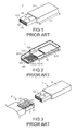
- FIG. 1 illustrates an external structural view of a conventional receiver
- FIG. 2 illustrates an internal structural view of a conventional receiver
- FIG. 3 illustrates a structural view of a connecting socket of a conventional receiver.
- the conventional receiver 1 comprises a circuit board 10, a body 11 I and a metal case 12.
- the body 11 has a carrying plate 111, the circuit board 10 is disposed within the body 11 and a front end 101 of the circuit board 10 is exposed outside the body 11, and the front end 101 of the circuit board 10 is disposed on the carrying plate 111.
- the front end 101 of the circuit board 10 is disposed with a plurality of electrical pins 1011, 1012, 1013 and 1014, and the electrical pins 1011, 1012, 1013 and 1014 are respectively a VCC power source circuit, a GND power source circuit, a D+ data transmission circuit and a D- data transmission circuit, wherein the D+ data transmission circuit and the D- data transmission circuit are used for data transmission, while the VCC power source circuit and the GND power source circuit are used for receiving an operating circuit provided by a female connecting socket 2 (as illustrated in FIG. 3 ) or a power supply.
- the metal case 12 encloses the front end 101 of the circuit board 10 in a manner of surrounding, so as to protect the circuit board 10.
- an inserting space 112 is formed between the front end 101 of the circuit board 10 and the metal 12, and thus the plurality of electrical pins 1011, 1012, 1013 and 1014 are exposed to the inserting space 112.
- the inserting space 112 is used for providing a space for fitting the conventional receiver 1 into the female connecting socket 2.
- the plurality of electrical pins 1011, 1012, 1013 and 1014 on the circuit board 10 connect with a plurality of connecting pins 21 of the female connecting socket 2 as illustrated in FIG. 3 .
- the circuit board 10 disposed within the body 11 further comprises a control circuit 102 and a memory unit 103.
- the memory unit 103 is used for storing data.
- two ends of the control circuit 102 respectively connect with the memory unit 103 and the plurality of electrical pins 1011, 1012, 1013 and 1014 as a control device for transmitting or storing data there-between.
- a portion of the body 11 of the conventional receiver 1 except the metal case 12 is defined as a holding portion, and users are capable of holding the conventional receiver 1 via the holding portion.
- a length of the holding portion of the conventional receiver 1 is L1
- the length of the holding portion depends on an arrangement of various electrical elements disposed on the circuit board 10 within the body 11.
- the conventional receiver 1 is received within the wireless peripheral device, and the holding portion of the conventional receiver 1 has a certain length, and thus the wireless peripheral device must have a certain volume for receiving the conventional receiver 1.
- the method for assembling the conventional receiver 1 comprises the following steps. First, the plurality of electrical pins 1011, 1012, 1013 and 1014 are respectively connected with the front end 101 of the circuit board 10 by a welding technology, and the control circuit 102 and the memory unit 103 are disposed on the circuit board 10 after that. Next, the circuit board 10 is disposed within the body 11. Finally, the metal case 12 is fit onto the front end 101 of the circuit board 10.
- the present invention is directed to a USB application device with a smaller volume.
- the present invention is further directed to a simpler method for assembling a USB application device.
- the present invention provides a USB application device capable of fitting into a female connecting socket, wherein the female connecting socket comprises a plurality of connecting pins, and the USB application device comprises:
- the present invention further comprises a case fitting onto the body, so as to form an inserting space between the case and the body.
- At least one of the plurality of electrical elements is disposed within the space formed between the pins plate and the circuit board.
- the body comprises:
- the body further comprises a hook portion disposed to a front end of the carrying portion and capable of supporting the circuit board, wherein the hook portion has an incline capable of guiding the circuit board to be put into the body.
- At least one of the plurality of electrical elements is disposed on a second end of at least one of the plurality of first electrical pins, and the second end is partly exposed within the space formed between the pins plate and the circuit board.
- At least one of the first electrical pins comprises an extending structure protruding from a second end of the at least one of the first electrical pins, and at least one of the plurality of electrical elements is capable of being disposed thereon.
- At least one of the first end and a second end of each one of the first electrical pins is mounted on the first surface of the circuit board by a surface mounted technology or a soldering technology.
- At least one of the plurality of first electrical pins comprises a first fixing segment, a second fixing segment, a first extending segment, a second extending segment and a contacting segment.
- the first fixing segment is the first end of each one of the first electrical pins
- the second fixing segment is a second end of each one of the first electrical pins.
- Both of the first extending segment and the second extending segment are located between the first surface of the circuit board and the body, and a first surface of the contacting segment is exposed by the body.
- the first surface of the contacting segment is capable of contacting with the connecting pins.
- a first bending structure is formed between the first extending segment and the contacting segment, while a second bending structure is formed between the second extending segment and the contacting segment, wherein the pins plate encloses the first extending segment and the second extending segment, while the pins plate partly encloses the contacting segment.
- the circuit board comprises a plurality of extending wires, and each one of the extending wires corresponds to one of the first electrical pins.
- Both of each one of the first fixing segments and each one of the second fixing segments connect with the circuit board and are adjacent to a front end of the circuit board, while each one of the extending wires connects with at least one of the corresponding one of the first fixing segments and the corresponding one of the second fixing segments and disposed along a direction extending toward a rear end of the circuit board, wherein the extending wires are directly formed on the circuit board.
- At least one of the plurality of first electrical pins comprises a fixing segment, a first extending segment, a second extending segment, a contacting segment and an incurvation segment.
- the fixing segment is the first end of at least one of the first electrical pins
- the incurvation segment is a second end of the at least one of the first electrical pins and partly exposed within the space formed between the pins plate and the circuit board without connecting with the circuit board.
- Both of the first extending segment and the second extending segment are located between the first surface of the circuit board and the body, and a first surface of the contacting segment is exposed by the body, wherein the first surface of the contacting segment is capable of contacting with the connecting pins.
- a first bending structure is formed between the first extending segment and the contacting segment, a second bending structure is formed between the second extending segment and the contacting segment, while a third bending structure is formed between the second extending segment and the incurvation segment, wherein the pins plate encloses the first extending segment and the second extending segment, while the pins plate partly encloses the contacting segment and the incurvation segment.
- the circuit board comprises a plurality of extending wires, and each one of the extending wires corresponds to one of the first electrical pins.
- Each of the fixing segments connects with the circuit board and is adjacent to a front end of the circuit board, while each one of the extending wires connects with the corresponding one of the fixing segments and is disposed along a direction extending toward a rear end of the circuit board, wherein the extending wires are directly formed on the circuit board.
- the USB application device of the present invention further comprises a plurality of second electrical pins disposed on the first surface of the circuit board and capable of contacting with a plurality of another connecting pins of the female connecting socket, wherein the plurality of first electrical pins form as a USB 2.0 transmission interface, while the plurality of first electrical pins and the plurality of second electrical pins form as a USB 3.0 transmission interface together.
- the USB application device of the present invention further comprises a plurality of third electrical pins disposed on a second surface of the circuit board and capable of contacting with the plurality of connecting pins of the female connecting socket, wherein the plurality of third electrical pins form as another USB 2.0 transmission interface, and thus both side of the USB application device are able to be plugged in.
- the pins plate partly enclosing the plurality of first electrical pins is formed by an embedded injection molding technology, and thus the pins plate partly encloses the plurality of the first electrical pins.
- the present invention further provides a method for assembling a USB application device, wherein the USB application device comprises a body and a circuit board, and the method comprises:
- the first end of each one of the first electrical pins disposed on the circuit board is mounted on the first surface of the circuit board by a surface mounted technology or a soldering technology.
- the circuit board comprises a plurality of extending wires, and each one of the extending wires corresponds to one of the first electrical pins.
- the first end of each one of the first electrical pins connects with the circuit board and is adjacent to a front end of the circuit board, while each one of the extending wires connects with the corresponding one of the first end and is disposed along a direction extending toward a rear end of the circuit board, wherein the extending wires are directly formed on the circuit board.
- the pins plate partly enclosing the plurality of first electrical pins is formed by an embedded injection molding technology.
- the body comprises a bottom and a carrying portion, and the carrying portion has a carrying portion aperture.
- the step of disposing the circuit board within the body comprises:
- the body comprises a hook portion and the hook portion has an incline.
- the step of turning the first end of the circuit board over comprises contacting the first end of the circuit board with the hook portion and then turning the first end over along the incline of the hook portion, so as to locate the first end of the circuit board within the body.
- the body comprises a bottom, a carrying portion and a plurality of column structures, and the carrying portion has a carrying portion aperture.
- the step of disposing the circuit board within the body comprises:
- the method further comprises fitting a case onto the body after disposing the circuit board within the body.
- the method further comprises disposing at least one of the plurality of electrical elements within the space formed between the pins plate and the circuit board when disposing the plurality of electrical elements and the plurality of first electrical pins on the circuit board.
- the method further comprises disposing at least one of the plurality of electrical elements to a second end of at least one of the plurality of first electrical pins after providing the pins plate and the pins plate partly enclosing the plurality of first electrical pins.
- the method further comprises disposing at least one of the plurality of electrical elements to a location adjacent to a second end of at least one of the plurality of first electrical pins after providing the pins plate and the pins plate partly enclosing the plurality of first electrical pins.
- FIG. 1 illustrates an external structural view of a conventional receiver.
- FIG. 2 illustrates an internal structural view of a conventional receiver.
- FIG. 3 illustrates a structural view of a connecting socket of a conventional receiver.
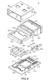
- FIG. 4 illustrates a structural explosion view of a USB application device according to a first preferred embodiment of the present invention.
- FIG. 5 illustrates an external structural view of a USB application device according to a first preferred embodiment of the present invention.
- FIG. 6 illustrates a structural cross-sectional view of a USB application device according to a first preferred embodiment of the present invention.
- FIG. 7 illustrates a block diagram of a method for assembling a USB application device according to a first preferred embodiment of the present invention.
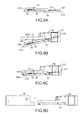
- FIG. 8A to FIG. 8D illustrate a structural side view of assembling a USB application device according to a first preferred embodiment of the present invention.
- FIG. 9 illustrates a structural explosion view of a USB application device from another angle of view according to a second preferred embodiment of the present invention.
- FIG. 10 illustrates an external structural view of a USB application device according to a second preferred embodiment of the present invention.
- FIG. 11 illustrates a structural cross-sectional view of a USB application device according to a second preferred embodiment of the present invention.
- FIG. 12 illustrates a block diagram of a method for assembling a USB application device according to a second preferred embodiment of the present invention.
- FIG. 13A to FIG. 13C illustrate a structural side view of assembling a USB application device according to a second preferred embodiment of the present invention.
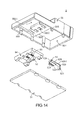
- FIG. 14 illustrates a structural explosion view of a USB application device from another angle of view according to a third preferred embodiment of the present invention.
- FIG. 15 illustrates a structural cross-sectional view of a USB application device according to a third preferred embodiment of the present invention.
- FIG. 16 illustrates a block diagram of a method for assembling a USB application device according to a third preferred embodiment of the present invention.
- FIG. 4 illustrates a structural explosion view of a USB application device according to a first preferred embodiment of the present invention.
- the USB application device 3 comprises a body 30, a circuit board 31, a plurality of first electrical pins 32, a plurality of electrical elements 33, a pins plate 34 and a case 35.
- the body 30 comprises a body opening 301, a carrying portion 302 and a hook portion 305, wherein the body opening 301 is disposed on a bottom 304 of the body 30, and thus a second surface 312 of the circuit board 31 is exposed by the body opening 301, while the carrying portion 302 is formed by extending from the body 30 toward a front end 303 of the body 30, and the carrying portion 302 has a carrying portion aperture 3021.
- the hook portion 305 is disposed to a front end 3022 of the carrying portion 302, and the hook portion 305 has an incline 3051.
- the circuit board 31 comprises a plurality of extending wires 315.
- Each of the extending wires 315 corresponds to one of the first electrical pins 32, and each one of the extending wires 315 is located on a first surface 311 of the circuit board 31 and disposed along a direction extending toward a second end 314 of the circuit board 31, wherein the plurality of extending wires 315 are directly formed on the first surface 311 of the circuit board 31.
- the first surface 311 is the upper surface of the circuit board 31
- the second surface 312 is the lower surface of the circuit board 31
- the second end 314 is the rear end of the circuit board 31.
- the plurality of electrical elements 33 are disposed to the first surface 311 of the circuit board 31.
- the pins plate 34 has a plurality of pins plate apertures 341 corresponding to the plurality of first electrical pins 32, wherein each one of the first electrical pins 32 is partly enclosed by the pins plate 34 and partly exposed outside the pins plate 34 by the corresponding one of the pins plate apertures 341.
- a first end 321 of each one of the first electrical pins 32 connects with the circuit board 31, passes over the first surface 311 of the circuit board 31 and extends toward the pins plate 34 in suspension, i.e.
- each one of the first electrical pins 32 crosses over at least one electrical element 33 of the plurality of electrical elements 33 on the circuit board 31.
- a space 36 is formed between the pins plate 34 partly enclosing each one of the first electrical pins 32 and the circuit board 31 (referring to FIG. 6 ), and thus at least one electrical element 33 of the plurality of electrical elements 33 can be disposed within the space 36.
- the pins plate 34 partly enclosing the plurality of first electrical pins 32 is formed by putting the plurality of first electrical pins 32 within a mold cavity to process an embedded injection molding technology, and the first ends 321 of the first electrical pins 32 and the second ends 322 of the first electrical pins 32 are exposed without being enclosed.
- the first ends 321 of the first electrical pins 32 are the front ends of the first electrical pins 32, while the second ends 322 of the first electrical pins 32 are the rear ends of the first electrical pins 32.
- the case 35 is capable of protecting the circuit board 31.
- the case 35 is made of metal materials.
- the case can also be made of plastic materials.
- FIG. 5 illustrates an external structural view of a USB application device according to a first preferred embodiment of the present invention
- FIG. 6 illustrates a structural cross-sectional view of a USB application device according to a first preferred embodiment of the present invention.
- the circuit board 31 is disposed within the body 30, and the pins plate 34 is put into the carrying portion aperture 3021 to combine the pins plate 34 with the body 30. Therefore, the pins plate 34 is exposed outside the carrying portion aperture 3021, and thus the plurality of first electrical pins 32, which is partly enclosed by the pins plate 34, can be partly exposed outside the body 30.
- each one of the first electrical pins 32 is defined as a first fixing segment 321 (i.e. the first end thereof), a second fixing segment 322 (i.e. the second end thereof), a first extending segment 323, a second extending segment 324 and a contacting segment 325.
- Both of the first fixing segment 321 and the second fixing segment 322 are exposed outside the pins plate 34 and are mounted on the circuit board 31 by a surface mounted technology (SMT), and the first fixing segment 321 and the second fixing segment 322 are adjacent to a first end 313 of the circuit board 31, wherein the first end 313 is the front end of the circuit board 31.
- SMT surface mounted technology
- FIG. 7 illustrates a block diagram of a method for assembling a USB application device according to a first preferred embodiment of the present invention
- FIG. 8A to FIG. 8D illustrate a structural side view of assembling a USB application device according to a first preferred embodiment of the present invention.
- the method for assembling the USB application device 3 comprises the following steps.
- a step S1 is providing a pins plate 34, wherein the pins plate 34 partly encloses a plurality of first electrical pins 32 as illustrated in FIG. 4 .
- the step S3 can further comprise a step S3-1 and a step S3-2.
- the step S3-1 is inserting the circuit board 31 into the bottom 304 of the body 30, and thus a second end 314 of the circuit board 31 passing through the bottom 304 and being put into the body 30 as illustrated in FIG. 8B .
- the step S3-2 is turning a first end 313 of the circuit board 31 over, and thus the first end 313 of the circuit board 31 passing through the bottom 304 and located within the body 30, and putting the pins plate 34 into the carrying portion aperture 3021 to combine the pins plate 34 with the body 30, and thus the plurality of first electrical pins 32 partly exposed by the body 30.
- FIG. 9 illustrates a structural explosion view of a USB application device from another angle of view according to a second preferred embodiment of the present invention.
- the USB application device 4 comprises a body 40, a circuit board 41, a plurality of first electrical pins 42, a plurality of electrical elements 43, a pins plate 44 and a plurality of third electrical pins 45.
- the body 40 comprises a body opening 401, a carrying portion 402 and a plurality of column structures 405.
- the body opening 401 is disposed on a bottom 404 of the body 40, so that a second surface 412 of the circuit board 41 is exposed by the body opening 401.
- the carrying portion 402 is formed by extending from the body 40 toward a front end 403 of the body 40, and the carrying portion 402 has a carrying portion aperture 4021.
- the plurality of column structures 405 are disposed at two opposite sides of a bottom 404 of the body 40, and the circuit board 41 has a plurality of notches 415.
- the plurality of notches 415 correspond to the plurality of column structures 405, and thus the circuit board 41 is capable of being directly inserted into the body 40 from the bottom 404 of the body 40 by matching up the plurality of notches 415 and the plurality of column structures 405.
- FIG. 10 illustrates an external structural view of a USB application device according to a second preferred embodiment of the present invention
- FIG. 11 illustrates a structural cross-sectional view of a USB application device according to a second preferred embodiment of the present invention.
- the circuit board 41 is disposed within the body 40, and the pins plate 44 are put into the carrying portion aperture 4021, so as to combine the pins plate 44 with the body 40.
- the pins plate 44 is exposed outside the carrying portion aperture 4021, and thus the plurality of first electrical pins 42, which are partly enclosed by the pins plate 44, can be partly exposed outside the body 40.
- the USB application device 4 is a thin type USB application device.
- a first surface 4251 of the contacting segment 425 is exposed by the body 40, and thus the first surface 4251 of the contacting segment 425 is able to contact with the connecting pins 21 of the female connecting socket 2 (referring to FIG. 3 ).
- a first bending structure 426 is formed between the first extending segment 423 and the contacting segment 425
- a second bending structure 427 is formed between the second extending segment 424 and the contacting segment 425, wherein the first bending structure 426 and the second bending structure 427 connect with the contacting segment 425 with an angle close to perpendicular or equal to perpendicular.
- the incurvation segment 422 is formed by extending from the second extending segment 424 without connecting with the circuit board 41.
- the incurvation segment 422 is partly exposed within a space 46 formed between the pins plate 44 and the circuit board 41, and thus at least one electrical element 44 of the plurality of electrical elements 44 is able to be disposed on the incurvation segment 422 (i.e. the second end 422 of the first electrical pin 42).
- a third bending structure 428 is formed between the second extending segment 424 and the incurvation segment 422.
- the pins plate 44 encloses the first extending segment 423 and the second extending segment 424, while the pins plate 44 partly encloses the contacting segment 425 and the incurvation segment 422.
- FIG. 12 illustrates a block diagram of a method for assembling a USB application device according to a second preferred embodiment of the present invention
- FIG. 13A to FIG. 13C illustrate a structural side view of assembling a USB application device according to a second preferred embodiment of the present invention.
- the method for assembling the USB application device 4 comprises the following steps.
- a step S1' is providing a pins plate 44, wherein the pins plate 44 partly encloses a plurality of first electrical pins 42.
- a step S2' is disposing at least one electrical element 43 of a plurality of electrical elements 43 to a second end 422 of at least one first electrical pin 42 of a plurality of first electrical pins 42.
- a step S3' is disposing the plurality of electrical elements 43 and the plurality of first electrical pins 42 on the circuit board 41, wherein a first end 421 of each one of the first electrical pins 42 connects with the circuit board 41, and each one of the first electrical pins 42 passes over a first surface 411 of the circuit board 41 and thus extends in suspension, so as to form a space 46 between the pins plate 44 and the circuit board 41.
- a step S4' is disposing the circuit board 41 within the body 40 and combining the pins plate 44 with the body 40, so that the plurality of first electrical pins 42 being partly exposed by the body 40.
- FIG. 14 illustrates a structural explosion view of a USB application device from another angle of view according to a third preferred embodiment of the present invention
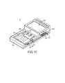
- FIG. 15 illustrates a structural cross-sectional view of a USB application device according to a third preferred embodiment of the present invention
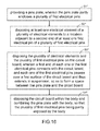
- FIG. 16 illustrates a block diagram of a method for assembling a USB application device according to a third preferred embodiment of the present invention.
- the USB application device 5 comprises a body 50, a circuit board 51, a plurality of first electrical pins 52, a plurality of electrical elements 53, a pins plate 54 and a plurality of second electrical pins 55.
- the body 50 comprises a body opening 501, a carrying portion 502 and a plurality of column structures 505, and the carrying portion 502 comprises a carrying portion aperture 5021 and a plurality of apertures 5022.
- each one of the first electrical pins 52 is defined as a first fixing segment 521 (i.e. the first end thereof), an incurvation segment 522 (i.e. the second end thereof), a first extending segment 523, a second extending segment 524 and a contacting segment 525.
- the structure of the USB application device 5 of the present preferred embodiment is substantially similar to that of the USB application device 4 of the second preferred embodiment and is omitted herein.
- At least one first electrical pin 52 of the plurality of first electrical pins 52 of the USB application device 5 of the present preferred embodiment further comprises an extending structure 5221, which is protruding from the incurvation segment 522 of the first electrical pin 52 (i.e. the second end thereof), and at least one electrical element 53 of the plurality of electrical elements 53 is capable of being disposed thereon.
- the extending structure 5221 is formed by protruding from a side edge of the incurvation segment 522, so that the electrical element 53 disposed on the extending structure 5221 will not be just located under the incurvation segment 522.
- the electrical element 53 can be disposed within a space 56 formed between the pins plate 54 and the circuit board 50, and the electrical element 53 can be disposed on the extending structure 5221 on the first electrical pin 52 as well.
- the length of the circuit board 51 can further be reduced due to the location available for disposing the electrical element 53 is increased. In a word, the volume of the USB application device 5 is reduced.
- the body 50 of the USB application device 5 of the present preferred embodiment further comprises a plurality of apertures 5022, and the plurality of apertures 5022 are adjacent to the carrying portion aperture 5021 and capable of being passed through by the plurality of second electrical pins 55 correspondingly.
- each one of the second electrical pins 55 is partly exposed by the corresponding aperture 5022.
- the plurality of first electrical pins 52 form as a USB 2.0 transmission interface
- the plurality of first electrical pins 52 and the plurality of second electrical pins 55 form as a USB 3.0 transmission interface together.
- the method for assembling the USB application device 5 of the present preferred embodiment comprises the following steps.
- a step S1* is providing a pins plate 54, wherein the pins plate 54 partly encloses a plurality of first electrical pins 52.
- a step S2* is disposing at least a electrical element 53 of a plurality of electrical elements 53 to a location 5221 adjacent to a second end 522 of at least a first electrical pin 52 of a plurality of first electrical pins 52.
- a step S3* is disposing the plurality of electrical elements 53 and the plurality of first electrical pins 52 on the circuit board 51, wherein a first end 521 of each one of the first electrical pins 52 connects with the circuit board 51, and each one of the first electrical pins 52 passes over a first surface 511 of the circuit board 51 and thus extends in suspension, so as to form a space 56 between the pins plate 54 and the circuit board 51.
- a step S4* is disposing the circuit board 51 within the body 50 and combining the pins plate 54 with the body 50, so that the plurality of first electrical pins 52 being partly exposed by the body 50 as illustrated in FIG. 15 .
- the method for assembling the USB application device 5 of the present preferred embodiment is substantially similar to the method for assembling the USB application device 4 of the second preferred embodiment, besides replacing the step S2' of the second preferred embodiment by using the step S2*, and the location 5221 adjacent to the second end 522 thereof is the extending structure 5221 formed by protruding from a side edge of the incurvation segment 522.
- the plurality of first electrical pins form as a stereoscopic structure due to the plurality of first electrical pins of the USB application device of the present invention are bent, and thus a space is formed between the circuit board and the plurality of first electrical pins for disposing the plurality of electrical elements therein or for other purpose.
- the electrical element of the USB application device of the present invention can be disposed to a portion of the first electrical pin being incurvated as well, i.e. the incurvation segment.
- the plurality of electrical elements originally disposed to the rear end of the circuit board can be moved to at least one of the three locations include the space between the plurality of first electrical pins and the circuit board, the incurvation segment and the extending structure. Therefore, the rear end of the circuit board does not need to be used anymore and can be omitted, and thus the length of the conventional circuit board can be reduced. As a result, the volume of the receiver can be further reduced.
- the plurality of electrical pins are previously disposed on the pins plate. Therefore, all of the first electrical pins are capable of being disposed on the circuit board by aligning the first electrical pins only one time during the process of combining the plurality of first electrical pins and the circuit board.
- the combination of the first electrical pins and the pins plate is designed accurately in order to contact with the plurality of connecting pins of the female connecting socket, and thus the plurality of first electrical pins are not likely to be askew or misaligned.
- the USB application device of the present invention can be used for various fields comprising storage or memory devices (such as flash devices, MP3 players), USB connecting plugs formed by combining with wires, and various receivers, wherein the various receivers comprise wireless mouse receivers, wireless keyboard receivers, Wi-Fi wireless network receivers and so on.
- storage or memory devices such as flash devices, MP3 players
- USB connecting plugs formed by combining with wires and various receivers, wherein the various receivers comprise wireless mouse receivers, wireless keyboard receivers, Wi-Fi wireless network receivers and so on.
Landscapes
- Engineering & Computer Science (AREA)
- Microelectronics & Electronic Packaging (AREA)
- Coupling Device And Connection With Printed Circuit (AREA)
Applications Claiming Priority (1)
| Application Number | Priority Date | Filing Date | Title |
|---|---|---|---|
| TW100142338A TWI459208B (zh) | 2011-11-18 | 2011-11-18 | 通用串列匯流排應用裝置以及通用串列匯流排應用裝置之組裝方法 |
Publications (1)
| Publication Number | Publication Date |
|---|---|
| EP2595464A2 true EP2595464A2 (en) | 2013-05-22 |
Family
ID=45400980
Family Applications (1)
| Application Number | Title | Priority Date | Filing Date |
|---|---|---|---|
| EP11194961.6A Withdrawn EP2595464A2 (en) | 2011-11-18 | 2011-12-21 | USB application device and method for assembling USB application device |
Country Status (4)
| Country | Link |
|---|---|
| US (1) | US8734182B2 (zh) |
| EP (1) | EP2595464A2 (zh) |
| JP (2) | JP2013109743A (zh) |
| TW (1) | TWI459208B (zh) |
Families Citing this family (7)
| Publication number | Priority date | Publication date | Assignee | Title |
|---|---|---|---|---|
| CN102496804A (zh) * | 2011-11-22 | 2012-06-13 | 华为终端有限公司 | Usb连接器及电子设备 |
| US9728917B2 (en) * | 2013-05-07 | 2017-08-08 | Alan L. Pocrass | High profile USB connector |
| JP6645413B2 (ja) * | 2016-12-15 | 2020-02-14 | 豊田合成株式会社 | 電子装置 |
| JP6559723B2 (ja) * | 2017-01-27 | 2019-08-14 | 矢崎総業株式会社 | 照明ユニット |
| USD891433S1 (en) | 2018-11-04 | 2020-07-28 | Kien Hoe Daniel Chin | USB adapter apparatus |
| USD885391S1 (en) | 2018-11-04 | 2020-05-26 | Kien Hoe Daniel Chin | USB adapter apparatus |
| US10797449B2 (en) * | 2019-03-05 | 2020-10-06 | Niceconn Technology Co., Ltd. | Connector having one-piece housing |
Family Cites Families (24)
| Publication number | Priority date | Publication date | Assignee | Title |
|---|---|---|---|---|
| US5364280A (en) * | 1993-07-16 | 1994-11-15 | Molex Incorporated | Printed circuit board connector assembly |
| US7249978B1 (en) * | 2005-10-24 | 2007-07-31 | Super Talent Electronics, Inc. | Reduced-length, low-profile USB device and card-like carrier |
| JP2001296708A (ja) * | 2000-04-13 | 2001-10-26 | Jst Mfg Co Ltd | トナーカートリッジ用コネクタ |
| CN2585308Y (zh) * | 2002-10-25 | 2003-11-05 | 互亿科技股份有限公司 | 兼具防水和导光性能的资讯装置 |
| TW565026U (en) * | 2003-01-24 | 2003-12-01 | C One Technology Corp | Small connector device |
| US7118646B2 (en) * | 2004-03-15 | 2006-10-10 | Delphi Technologies, Inc. | Method of manufacturing a sealed electronic module |
| TWM266601U (en) * | 2004-10-22 | 2005-06-01 | Chen Guo Liang | Card insertion type connector |
| JP4434121B2 (ja) * | 2005-09-30 | 2010-03-17 | Tdk株式会社 | コネクタ |
| TW200849747A (en) * | 2007-06-15 | 2008-12-16 | Transcend Information Inc | USB connector device, connector module and manufacturing method |
| US7618293B2 (en) * | 2007-11-02 | 2009-11-17 | Hon Hai Precision Ind. Co., Ltd. | Extension to electrical connector with improved housing structures |
| TW201014495A (en) * | 2008-09-19 | 2010-04-01 | Fih Hong Kong Ltd | Connector shell structure and electronic device using the same |
| TW201017369A (en) * | 2008-10-22 | 2010-05-01 | Kye Systems Corp | USB device |
| TWM364982U (en) * | 2008-12-22 | 2009-09-11 | nai-qian Zhang | Connector with storage function |
| TWM364253U (en) * | 2009-04-17 | 2009-09-01 | Good Way Technology Co Ltd | USB information device |
| JP2010267260A (ja) * | 2009-04-20 | 2010-11-25 | Moser Baer India Ltd | 小型メモリ装置 |
| JP2010267484A (ja) * | 2009-05-14 | 2010-11-25 | Mitsubishi Electric Corp | 信号等化器 |
| US7717717B1 (en) * | 2009-06-26 | 2010-05-18 | Joseph Lai | User-friendly USB connector |
| US8323057B2 (en) * | 2010-08-13 | 2012-12-04 | Molex Incorporated | Receptacle connector |
| US20120071032A1 (en) * | 2010-09-17 | 2012-03-22 | Tsai Chou-Hsien | Electrical receptacle |
| CN102412473B (zh) * | 2010-09-21 | 2014-07-02 | 富士康(昆山)电脑接插件有限公司 | 线缆连接器组件 |
| CN102412456B (zh) * | 2010-09-21 | 2014-09-24 | 富士康(昆山)电脑接插件有限公司 | 电连接器 |
| TW201214884A (en) * | 2010-09-27 | 2012-04-01 | Chou-Hsien Tsai | Electrical receptacle |
| TWM412498U (en) * | 2011-05-12 | 2011-09-21 | Power Quotient Int Co Ltd | USB connector |
| TWI525951B (zh) * | 2011-09-09 | 2016-03-11 | 致伸科技股份有限公司 | 通用串列匯流排應用裝置以及通用串列匯流排應用裝置之組裝方法 |
-
2011
- 2011-11-18 TW TW100142338A patent/TWI459208B/zh not_active IP Right Cessation
- 2011-12-21 EP EP11194961.6A patent/EP2595464A2/en not_active Withdrawn
- 2011-12-21 JP JP2011280042A patent/JP2013109743A/ja active Pending
-
2012
- 2012-03-09 US US13/417,011 patent/US8734182B2/en not_active Expired - Fee Related
-
2016
- 2016-06-24 JP JP2016125039A patent/JP6190004B2/ja active Active
Non-Patent Citations (1)
| Title |
|---|
| None |
Also Published As
| Publication number | Publication date |
|---|---|
| TW201321990A (zh) | 2013-06-01 |
| US20130130517A1 (en) | 2013-05-23 |
| JP2016181283A (ja) | 2016-10-13 |
| JP2013109743A (ja) | 2013-06-06 |
| US8734182B2 (en) | 2014-05-27 |
| JP6190004B2 (ja) | 2017-08-30 |
| TWI459208B (zh) | 2014-11-01 |
Similar Documents
| Publication | Publication Date | Title |
|---|---|---|
| US8734182B2 (en) | USB application device and method for assembling USB application device | |
| JP6284991B2 (ja) | 外部接点を有する双配向電子コネクタ | |
| EP2425502B1 (en) | Connector arrangement | |
| US8430690B2 (en) | USB application device and method for assembling USB application device | |
| TWM582251U (zh) | Connector set with built-in locking mechanism and socket connector thereof | |
| CN203813095U (zh) | 电连接器之插座 | |
| US9190781B2 (en) | Stacking connector having detection function | |
| US20080050971A1 (en) | Adaptor and wireless communication module | |
| TWM458687U (zh) | 具訊號處理ic的usb連接器及usb傳輸線 | |
| US9455528B1 (en) | Multi-plug USB connector with swappable tip | |
| US9270038B1 (en) | Multi-plug USB connector with swappable tip | |
| US7231236B2 (en) | Integrated antenna and input/output port for a wireless communication device | |
| US20070072491A1 (en) | Integrated signal connecting port | |
| TWI445264B (zh) | 連接器插座及其製造方法 | |
| KR101348141B1 (ko) | 멀티형 리셉터클 커넥터 및 이에 적용되는 플러그 커넥터 | |
| TWM531072U (zh) | 卡連接器 | |
| CN201774000U (zh) | 端子及使用该端子的电连接器 | |
| KR102286609B1 (ko) | 유에스비 커넥터와 그 제조 방법 및 이를 구비하는 전자 기기 | |
| CN219801409U (zh) | 具有多个接地路径所形成屏蔽机制的连接器 | |
| CN104134909B (zh) | 连接器 | |
| CN217468973U (zh) | 具有导引结构的连接器组及其插头连接器与插座连接器 | |
| TWI625013B (zh) | Dual-purpose connector plug and USB cable with dual-purpose connector plug | |
| TWM631762U (zh) | 具有導引結構的連接器組及其插頭連接器與插座連接器 | |
| KR20040077018A (ko) | 인쇄회로기판 실장형 유에스비 미니비 플러그 | |
| TWM529306U (zh) | 雙用途連接插頭及具有雙用途連接插頭的usb連接線 |
Legal Events
| Date | Code | Title | Description |
|---|---|---|---|
| PUAI | Public reference made under article 153(3) epc to a published international application that has entered the european phase |
Free format text: ORIGINAL CODE: 0009012 |
|
| AK | Designated contracting states |
Kind code of ref document: A2 Designated state(s): AL AT BE BG CH CY CZ DE DK EE ES FI FR GB GR HR HU IE IS IT LI LT LU LV MC MK MT NL NO PL PT RO RS SE SI SK SM TR |
|
| AX | Request for extension of the european patent |
Extension state: BA ME |
|
| STAA | Information on the status of an ep patent application or granted ep patent |
Free format text: STATUS: THE APPLICATION IS DEEMED TO BE WITHDRAWN |
|
| 18D | Application deemed to be withdrawn |
Effective date: 20170701 |