EP2595185A2 - Vorrichtung mit einem integrierten Schaltkreis - Google Patents
Vorrichtung mit einem integrierten Schaltkreis Download PDFInfo
- Publication number
- EP2595185A2 EP2595185A2 EP12004724.6A EP12004724A EP2595185A2 EP 2595185 A2 EP2595185 A2 EP 2595185A2 EP 12004724 A EP12004724 A EP 12004724A EP 2595185 A2 EP2595185 A2 EP 2595185A2
- Authority
- EP
- European Patent Office
- Prior art keywords
- contact
- terminal
- connection
- connection contact
- capacitor
- Prior art date
- Legal status (The legal status is an assumption and is not a legal conclusion. Google has not performed a legal analysis and makes no representation as to the accuracy of the status listed.)
- Granted
Links
Images

Classifications
-
- H—ELECTRICITY
- H10—SEMICONDUCTOR DEVICES; ELECTRIC SOLID-STATE DEVICES NOT OTHERWISE PROVIDED FOR
- H10W—GENERIC PACKAGES, INTERCONNECTIONS, CONNECTORS OR OTHER CONSTRUCTIONAL DETAILS OF DEVICES COVERED BY CLASS H10
- H10W72/00—Interconnections or connectors in packages
-
- H—ELECTRICITY
- H10—SEMICONDUCTOR DEVICES; ELECTRIC SOLID-STATE DEVICES NOT OTHERWISE PROVIDED FOR
- H10W—GENERIC PACKAGES, INTERCONNECTIONS, CONNECTORS OR OTHER CONSTRUCTIONAL DETAILS OF DEVICES COVERED BY CLASS H10
- H10W70/00—Package substrates; Interposers; Redistribution layers [RDL]
- H10W70/40—Leadframes
- H10W70/475—Capacitors in combination with leadframes
-
- H—ELECTRICITY
- H10—SEMICONDUCTOR DEVICES; ELECTRIC SOLID-STATE DEVICES NOT OTHERWISE PROVIDED FOR
- H10W—GENERIC PACKAGES, INTERCONNECTIONS, CONNECTORS OR OTHER CONSTRUCTIONAL DETAILS OF DEVICES COVERED BY CLASS H10
- H10W70/00—Package substrates; Interposers; Redistribution layers [RDL]
- H10W70/40—Leadframes
- H10W70/481—Leadframes for devices being provided for in groups H10D8/00 - H10D48/00
-
- H—ELECTRICITY
- H10—SEMICONDUCTOR DEVICES; ELECTRIC SOLID-STATE DEVICES NOT OTHERWISE PROVIDED FOR
- H10W—GENERIC PACKAGES, INTERCONNECTIONS, CONNECTORS OR OTHER CONSTRUCTIONAL DETAILS OF DEVICES COVERED BY CLASS H10
- H10W72/00—Interconnections or connectors in packages
- H10W72/50—Bond wires
- H10W72/541—Dispositions of bond wires
- H10W72/5449—Dispositions of bond wires not being orthogonal to a side surface of the chip, e.g. fan-out arrangements
-
- H—ELECTRICITY
- H10—SEMICONDUCTOR DEVICES; ELECTRIC SOLID-STATE DEVICES NOT OTHERWISE PROVIDED FOR
- H10W—GENERIC PACKAGES, INTERCONNECTIONS, CONNECTORS OR OTHER CONSTRUCTIONAL DETAILS OF DEVICES COVERED BY CLASS H10
- H10W90/00—Package configurations
- H10W90/701—Package configurations characterised by the relative positions of pads or connectors relative to package parts
- H10W90/751—Package configurations characterised by the relative positions of pads or connectors relative to package parts of bond wires
- H10W90/756—Package configurations characterised by the relative positions of pads or connectors relative to package parts of bond wires between a chip and a stacked lead frame, conducting package substrate or heat sink
Definitions
- the invention relates to a device with an integrated circuit according to the preamble of patent claim 1.
- an integrated circuit device includes an integrated circuit incorporated in a circuit package, a plurality of terminals, and a discrete capacitor integrated in the circuit package.
- a first connection contact for the voltage supply and a second connection contact are connected to a reference potential.
- the object of the invention is to provide a device which further develops the prior art.
- an apparatus comprising an integrated circuit and a circuit package having a first terminal contact and a second terminal contact and a third terminal contact, wherein the first terminal contact and the second terminal contact and the third terminal contact are led out of the circuit housing, and the first terminal contact is designed as a voltage supply terminal and the second terminal contact is designed as a reference potential terminal and the first terminal contact and the second terminal contact are connected within the circuit housing to the integrated circuit and the third terminal contact in the circuit housing as a signal transmission terminal is connected to the integrated circuit, and a first capacitor and a second capacitor, wherein the first capacitor and the second capacitor are integrated into the circuit housing and the first capacitor to the first terminal and the second capacitor is connected to the third terminal contact, wherein a fourth terminal and a fifth terminal are provided, and the fourth terminal and the fifth terminal are respectively led out of the circuit housing, and the first capacitor is connected to the fourth terminal and the second capacitor is connected to the fifth terminal.
- first capacitor forms a connection between the first connection contact and the fourth connection contact.
- second capacitor forms a connection between the third connection contact and the fifth connection contact.
- each of the first connection contact, the second connection contact, the third connection contact, the fourth connection contact and the fifth connection contact are different connection contacts.
- An advantage is that the integration of capacitors, which are not already connected to the respective second terminal of the respective capacitor with a reference potential, preferably to the ground potential, can open up additional applications for the device, without resulting in an integration of the capacitors affect the measuring program or measuring routines. Due to the advantageous connection of the capacitors, the measuring times at the connection contacts of the supply voltage and the reference potential, especially in a final test of the circuits in a comparison to the measuring times of the respective terminals without connected integrated capacitors are not extended. Also, measurements in the high-frequency range, for example, above 1 MHz, the measurement results are not distorted by the integrated capacitors. Furthermore, the integrated capacitors can be connected to the reference potential as well as to other external circuit components both before and after the final test measurement. By additionally inserting freely configurable connection contacts in the present case, the flexibility of the device can be considerably increased.
- the device is characterized in that the fourth connection contact between the first connection contact and the second connection contact is arranged, and the fifth connection contact between the second connection contact and the third connection contact is arranged.
- the second terminal contact and / or the fourth terminal contact and / or the fifth terminal contact outside the circuit housing in a first third of the outside of the circuit housing formed overall length of the terminal contacts are shorted together.
- the second connection contact and / or the fourth terminal contact and / or the fifth terminal contact outside the circuit housing in a third third of the outside of the circuit housing formed overall length of the terminal contacts shorted together.
- a particular advantage of the embodiments is that by connecting the terminal contacts, a different functionality of the device arises in comparison to the previous developments.
- the other functionality is, for example, that the integrated capacitors, in contrast to the test mode, i. E. in an operation with capacitors connected only on one side, the capacitors now act as interference suppression filters on the supply voltage. It is advantageous that the functionality can be produced at any time. Investigations have shown that the device can be delivered without the short circuit, the second connection contact and / or the fourth connection contact and / or the fifth connection contact and thereby provides a user with a high degree of flexibility in terms of circuitry. In this case, it is particularly advantageous that, despite the introduction of two additional connection contacts, a cost saving is created by means of a reduced outlay in the test of the circuits during the production.
- the picture of the FIG. 1 1 shows a schematic view of a first embodiment of a device 1 comprising a circuit housing 5 and a circuit 10 integrated within the circuit housing 5.
- the connection contacts 41, 42, 43, 44, 45 are arranged in a row and parallel to each other.
- the first connection contact 41 is followed, from left to right, by the fourth connection contact 44, hereinafter the second connection contact 42, hereafter the fifth connection contact 45 and, lastly, the third connection contact 43.
- the first connection contact 41 is in the circuit housing 5 via a first bonding wire 51 a first contact surface 61 is connected to the integrated circuit 10.
- the second terminal contact 42 is connected in the circuit housing 5 via a second bonding wire 52 to a second contact surface 62 on the integrated circuit 10.
- the third connection contact 43 is connected in the circuit housing 5 via a third bonding wire 53 to a third contact surface 63 on the integrated circuit 10.
- a first capacitor 31 and a second capacitor 32 are also integrated.
- the first capacitor 31 is connected to the first connection contact 41 and to the fourth connection contact 44.
- the second capacitor 32 is connected to the third terminal contact 43 and to the fifth terminal contact 45.
- a further embodiment of the device 1 is shown. The following are just the differences from the illustration of FIG. 1 explained.
- a wire bridge 70 is formed at right angles between the connection contacts 42, 44, 45. The wire bridge 70 establishes a short circuit between the fourth connection contact 44, the third connection contact 43 and the fifth connection contact 45.
- a wire bridge 70 is formed parallel to the circuit housing 5.
- the wire bridge 70 establishes a short circuit between the fourth connection contact 44, the third connection contact 43 and the fifth connection contact 45 and is formed, for example, from a metal strip.
- the metal strip is directly connected, for example, by soldering to the second connection contact 42 and the fourth connection contact 44 and the fifth connection contact 45.
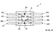
- FIG. 4 a further embodiment of the device 1 is shown.
- the circuit housing 5 now has a sixth connection contact 46, a seventh connection contact 47 and an eighth connection contact 48.
- the terminal contacts 41, 48, 47, and 45 are disposed on opposite sides of the circuit housing 5 with respect to the terminal contacts 44, 46, 42, and 43.
- the additional connection contacts 46, 47, 48 are preferably designed as signal connections for integrated circuit 10.
- terminals are arranged quite differently depending on the design of the circuit housing and not in a row. Accordingly, can be in other circuit packages capacitors and in particular integrate further passive components with additional connection contacts according to the present inventive idea in the circuit housing.
- FIG. 5 is a device according to the prior art, as already mentioned in the introduction, depicted in abstracted form.
Landscapes
- Semiconductor Integrated Circuits (AREA)
- Details Of Connecting Devices For Male And Female Coupling (AREA)
- Engineering & Computer Science (AREA)
- Power Engineering (AREA)
Abstract
Description
- Die Erfindung betrifft eine Vorrichtung mit einem integrierten Schaltkreis gemäß dem Oberbegriff des Patentanspruchs 1.
- Aus der
JP 57118661 A - Des Weiteren ist aus der Druckschrift
DE 101 02 440 C1 ein Schaltkreisgehäuse für eine integrierte Schaltung und einen zusätzlich in das Schaltkreisgehäuse integrierten diskreten Kondensator bekannt. - Vor diesem Hintergrund besteht die Aufgabe der Erfindung darin, eine Vorrichtung anzugeben, die den Stand der Technik weiterbildet.
- Die Aufgabe wird durch eine Vorrichtung mit den Merkmalen des Patentanspruchs 1 gelöst. Vorteilhafte Ausgestaltungen der Erfindung sind in den Unteransprüchen enthalten.
- Gemäß dem Gegenstand der Erfindung wird eine Vorrichtung bereitgestellt, aufweisend einen integrierten Schaltkreis und ein Schaltkreisgehäuse mit einem ersten Anschlusskontakt und einem zweiten Anschlusskontakt und einem dritten Anschlusskontakt, wobei der erste Anschlusskontakt und der zweite Anschlusskontakt und der dritte Anschlusskontakt aus dem Schaltkreisgehäuse herausgeführt sind, und der erste Anschlusskontakt als Spannungsversorgungsanschluss und der zweite Anschlusskontakt als Bezugspotentialanschluss ausgebildet ist und der erste Anschlusskontakt und der zweite Anschlusskontakt innerhalb des Schaltkreisgehäuses mit dem integrierten Schaltkreis verbunden sind und der dritte Anschlusskontakt im Schaltkreisgehäuse als Signalübertragungsanschluss mit dem integrierten Schaltkreis verschaltet ist, sowie einen ersten Kondensator und einen zweiten Kondensator, wobei der erste Kondensator und der zweite Kondensator in das Schaltkreisgehäuse integriert sind und der erste Kondensator an den ersten Anschlusskontakt und der zweite Kondensator an den dritten Anschlusskontakt angeschlossen ist, wobei ein vierter Anschlusskontakt und ein fünfter Anschlusskontakt vorgesehen sind und der vierte Anschlusskontakt und der fünfte Anschlusskontakt jeweils aus dem Schaltkreisgehäuse herausgeführt sind, und der erste Kondensator an den vierten Anschlusskontakt und der zweite Kondensator an den fünften Anschlusskontakt angeschlossen sind.
- Es sei angemerkt, dass der erste Kondensator eine Verbindung zwischen dem ersten Anschlusskontakt und dem vierten Anschlusskontakt bildet. Weiterhin bildet der zweite Kondensator eine Verbindung zwischen dem dritten Anschlusskontakt und dem fünften Anschlusskontakt. Ferner handelt es sich jeweils bei dem ersten Anschlusskontakt, dem zweiten Anschlusskontakt, dem dritten Anschlusskontakt, dem vierten Anschlusskontakt und dem fünften Anschlusskontakt um unterschiedliche Anschlusskontakte.
- Ein Vorteil ist, dass durch die Integration von Kondensatoren, welche nicht bereits mit dem jeweiligen zweiten Anschluss des jeweiligen Kondensators mit einem Bezugspotential, vorzugsweise mit dem Massepotential, verschaltet sind, sich zusätzliche Anwendungen für die Vorrichtung erschließen lassen, ohne dass sich eine Integration der Kondensatoren auf das Messprogramm bzw. die Messroutinen auswirken. Durch die vorteilhafte Anschlussweise der Kondensatoren werden die Messzeiten an den Anschlusskontakten der Versorgungsspannung und dem Bezugspotential insbesondere bei einem Final Test der Schaltkreise bei einem Vergleich zu den Messzeiten der jeweiligen Anschlusskontakte ohne angeschlossene integrierte Kondensatoren nicht verlängert. Auch werden bei Messungen im hochfrequenten Bereich, beispielsweise oberhalb 1 MHz, die Messergebnisse durch die integrierten Kondensatoren nicht verfälscht. Des Weiteren lassen sich die integrierten Kondensatoren sowohl vor, als auch nach der Final Testmessung noch mit dem Bezugspotential als auch mit weiteren externen Schaltungskomponenten verbinden. Indem vorliegend zusätzlich frei konfigurierbare Anschlusskontakte eingefügt werden, lässt sich die Flexibilität der Vorrichtung erheblich steigern.
- In einer Ausführungsform besteht zwischen dem vierten Anschlusskontakt und dem integrierten Schaltkreis innerhalb des Schaltkreisgehäuses kein elektrischer Anschluss. Gemäß einer anderen Ausführungsform ist zwischen dem fünften Anschlusskontakt und dem integrierten Schaltkreis innerhalb des Schaltkreisgehäuses kein elektrischer Anschluss ausgebildet. Ein Vorteil der beiden vorangestellten Ausführungsformen, d.h. mittels des einseitigen Anschlusses besteht darin, dass ein Test des integrierten Schaltkreises, ohne Auswirkungen auf den integrierten Schaltkreis durch die Integration des ersten Kondensators und oder des zweiten Kondensators durchführen lässt. Hierzu wird in einem ersten Schritt ausschließlich der erste Anschlusskontakt und / oder der zweite Anschlusskontakt und / oder der dritte Anschlusskontakt an eine Testeinrichtung angeschlossen.
- In einer Weiterbildung ist die Vorrichtung dadurch gekennzeichnet, dass der vierte Anschlusskontakt zwischen dem ersten Anschlusskontakt und dem zweiten Anschlusskontakt angeordnet ist, und der fünfte Anschlusskontakt zwischen dem zweiten Anschlusskontakt und dem dritten Anschlusskontakt angeordnet ist. Ein Vorteil der Anordnung liegt in einer einfachen Verbindungsmöglichkeit des zweiten als Bezugspotentialanschluss ausgeführten Anschlusskontakts mit dem vierten Anschlusskontakt und / oder dem fünften Anschlusskontakt. Durch das unmittelbare Aufeinanderfolgen der drei Anschlusskontakte lassen sich beispielsweise einfache gerade Drahtabschnitte oder Drahtbrücken zu einem Verbinden der unmittelbar benachbarten Anschlusskontakte verwenden, ohne eine Ausbildung von speziell geformten Drähten für ein Ausblenden von nicht zu verbindenden Anschlusskontakten.
- Gemäß einer anderen Ausführungsform sind der zweite Anschlusskontakt und / oder der vierte Anschlusskontakt und / oder der fünfte Anschlusskontakt außerhalb des Schaltkreisgehäuses in einem ersten Drittel der außerhalb des Schaltkreisgehäuses ausgebildeten Gesamtlänge der Anschlusskontakten miteinander kurzgeschlossen. Alternativ oder zusätzlich sind der zweite Anschlusskontakt und / oder der vierte Anschlusskontakt und / oder der fünfte Anschlusskontakt außerhalb des Schaltkreisgehäuses in einem dritten Drittel der außerhalb des Schaltkreisgehäuses ausgebildeten Gesamtlänge der Anschlusskontakten miteinander kurzgeschlossen.
- Ein besonderer Vorteil der Ausführungsformen ist es, dass durch das Verbinden der Anschlusskontakte eine andere Funktionalität der Vorrichtung im Vergleich zu den vorhergehenden Weiterbildungen entsteht. Die andere Funktionalität besteht beispielsweise darin, dass die integrierten Kondensatoren, im Gegensatz zum Testbetrieb, d.h. in einem Betrieb mit nur einseitig angeschlossenen Kondensatoren, die Kondensatoren nunmehr als Entstörfilter auf die Versorgungsspannung wirken. Vorteilhaft ist dabei, dass sich die Funktionalität jederzeit herstellen lässt. Untersuchungen haben gezeigt, dass sich die Vorrichtung ohne den Kurzschluss, des zweiten Anschlusskontaktes und / oder des vierten Anschlusskontaktes und / oder des fünften Anschlusskontaktes ausliefern lässt und hierdurch einem Anwender eine hohe schaltungstechnische Flexibilität zur Verfügung stellt. Besonders vorteilhaft ist hierbei, dass bei der Herstellung trotz der Einführung von zwei zusätzlichen Anschlusskontakten eine Kosteneinsparung mittels eines reduzierten Aufwandes bei dem Test der Schaltkreise entsteht.
- Die Erfindung wird nachfolgend unter Bezugnahme auf die Zeichnungen näher erläutert. Hierbei werden gleichartige Teile mit identischen Bezeichnungen beschriftet. Die dargestellte Ausführungsformen sind stark schematisiert, d.h. die Abstände und laterale und vertikale Erstreckung sind nicht maßstäblich und weisen, sofern nicht anders angegeben auch keine ableitbare geometrische Relation zueinander auf. Darin zeigen die:
- Figur 1
- eine schematische Ansicht auf eine erste erfindungsgemäße Ausführungsform der Vorrichtung,
- Figur 2
- eine schematische Ansicht auf eine zweite erfindungsgemäße Ausführungsform der Vorrichtung,
- Figur 3
- eine schematische Ansicht auf eine dritte erfindungsgemäße Ausführungsform der Vorrichtung,
- Figur 4
- eine schematische Ansicht auf eine vierte erfindungsgemäße Ausführungsform der Vorrichtung,
- Figur 5
- eine schematische Ansicht auf eine Vorrichtung gemäß dem Stand der Technik.
- Die Abbildung der
Figur 1 zeigt eine schematische Ansicht einer ersten Ausführungsform einer Vorrichtung 1, aufweisend ein Schaltkreisgehäuse 5 und einen innerhalb des Schaltkreisgehäuses 5 integrierten- Schaltkreis 10. Aus dem Schaltkreisgehäuse 5 sind ein erster Anschlusskontakt 41 und ein zweiter Anschlusskontakt 42 und ein dritter Anschlusskontakt 43 und ein vierter Anschlusskontakt 44 und ein fünfter Anschlusskontakt 45 herausgeführt. Die Anschlusskontakte 41, 42, 43, 44, 45 sind in einer Reihe und parallel zueinander angeordnet. Auf den ersten Anschlusskontakt 41 folgt, von links nach rechts, der vierte Anschlusskontakt 44, hiernach der zweite Anschlusskontakt 42, hiernach der fünfte Anschlusskontakt 45 und als letztes der dritte Anschlusskontakt 43. Der erste Anschlusskontakt 41 ist im Schaltkreisgehäuse 5 über einen ersten Bonddraht 51 an eine erste Kontaktfläche 61 auf dem integrierten Schaltkreis 10 angeschlossen. Der zweite Anschlusskontakt 42 ist im Schaltkreisgehäuse 5 über einen zweiten Bonddraht 52 an eine zweite Kontaktfläche 62 auf dem integrierten Schaltkreis 10 angeschlossen. Der dritte Anschlusskontakt 43 ist im Schaltkreisgehäuse 5 über einen dritten Bonddraht 53 an eine dritte Kontaktfläche 63 auf dem integrierten Schaltkreis 10 angeschlossen. In das Schaltkreisgehäuse sind außerdem ein erster Kondensator 31 und ein zweiter Kondensator 32 integriert. Der erste Kondensator 31 ist an den ersten Anschlusskontakt 41 und an den vierten Anschlusskontakt 44 angeschlossen. Der zweite Kondensator 32 ist an den dritten Anschlusskontakt 43 und an den fünften Anschlusskontakt 45 angeschlossen. - In der Abbildung der
Figur 2 ist eine weitere Ausführungsform der Vorrichtung 1 dargestellt. Im Folgenden werden nur die Unterschiede zu der Abbildung derFigur 1 erläutert. Am unteren Ende, d.h. im dritten Drittel der Anschlusskontakte 42, 44, 45 ist eine Drahtbrücke 70 rechtwinklig zwischen den Anschlusskontakten 42, 44, 45 ausgebildet. Die Drahtbrücke 70 stellt einen Kurzschluss zwischen dem vierten Anschlusskontakt 44, dem dritten Anschlusskontakt 43 und dem fünften Anschlusskontakt 45 her. - In der Abbildung der
Figur 3 ist eine weitere Ausführungsform der Vorrichtung 1 dargestellt. Im Folgenden werden nur die Unterschiede zu der Abbildung derFigur 1 erläutert. Außerhalb des Schaltkreisgehäuses 5, unmittelbar an der Stelle der Herausführung der Anschlusskontakte 42, 44, 45, d.h. in einem ersten Drittel, ist eine Drahtbrücke 70 parallel zu dem Schaltkreisgehäuse 5 ausgebildet. Die Drahtbrücke 70 stellt einen Kurzschluss zwischen dem vierten Anschlusskontakt 44, dem dritten Anschlusskontakt 43 und dem fünften Anschlusskontakt 45 her und ist beispielsweise aus einem Metallstreifen ausgebildet. Der Metallstreifen ist beispielsweise durch eine Lötung mit dem zweiten Anschlusskontakt 42 und dem vierten Anschlusskontakt 44 und dem fünften Anschlusskontakt 45 unmittelbar verbunden. - In der Abbildung der
Figur 4 ist eine weitere Ausführungsform der Vorrichtung 1 dargestellt. Im Folgenden werden nur die Unterschiede zu der Abbildung der vorangegangen Figuren erläutert. Demgemäß wird eine weitere Form des Schaltkreisgehäuses 5 angeführt. Das Schaltkreisgehäuse 5 weist nunmehr einen sechsten Anschlusskontakt 46, einen siebten Anschlusskontakt 47 und einen achten Anschlusskontakt 48 auf. Ferner sind die Anschlusskontakte 41, 48, 47 und 45 in Bezug auf die Anschlusskontakte 44, 46, 42 und 43 auf gegenüberliegenden Seiten des Schaltkreisgehäuses 5 angeordnet. Die zusätzlichen Anschlusskontakte 46, 47, 48 sind bevorzugt als Signalanschlüsse für integrierten Schaltkreis 10 ausgeführt. - Es versteht sich, dass die Anschlusskontakte je nach Ausführung der Schaltkreisgehäuse ganz unterschiedlich und nicht in einer Reihe angeordnet sind. Demgemäß lassen sich auch in weiteren Schaltkreisgehäusen Kondensatoren und insbesondere auch weitere passive Bauelemente mit zusätzlichen Anschlusskontakten entsprechend der vorliegenden erfinderischen Idee in das Schaltkreisgehäuse integrieren.
- In der
Figur 5 ist eine Vorrichtung nach dem Stand der Technik, wie bereits in der Beschreibungseinleitung erwähnt, in abstrahierter Form abgebildet. -
- 1
- Vorrichtung
- 5
- Schaltkreisgehäuse
- 10
- integrierter Schaltkreis, Halbleiterchip
- 31
- Erster Kondensator
- 32
- Zweiter Kondensator
- 41
- Erster Anschlüsskontakt
- 42
- Zweiter Anschlusskontakt
- 43
- Dritter Anschlusskontakt
- 44
- Vierter Anschlusskontakt
- 46
- Sechster Anschlusskontakt
- 47
- Siebter Anschlusskontakt
- 48
- Achter Anschlusskontakt
- 45
- Fünfter Anschlusskontakt
- 51
- Erster Bonddraht
- 52
- Zweiter Bonddraht .
- 53
- Dritter Bonddraht
- 61
- Erste Kontaktfläche
- 62
- Zweite Kontaktfläche
- 63
- Dritte Kontaktfläche
- 70
- Drahtbrücke
Claims (6)
- Vorrichtung (1) aufweisend,
einen integrierten Schaltkreis (10) und ein Schaltkreisgehäuse (5) mit einem ersten Anschlusskontakt (41) und einem zweiten Anschlusskontakt (42) und einem dritten Anschlusskontakt (43), wobei der erste Anschlusskontakt (41) und der zweite Anschlusskontakt (42) und der dritte Anschlusskontakt (43) aus dem Schaltkreisgehäuse (5) herausgeführt sind, und der erste Anschlusskontakt (41) als Spannungsversorgungsanschluss und der zweite Anschlusskontakt (42) als Bezugspotentialanschluss ausgebildet ist und der erste Anschlusskontakt (41) und der zweite Anschlusskontakt (42) innerhalb des Schaltkreisgehäuses (5) mit dem integrierten Schaltkreis (10) verbunden sind und der dritte Anschlusskontakt (43) im Schaltkreisgehäuse (5) als Signalübertragungsanschluss mit dem integrierten Schaltkreis (10) verschaltet ist, sowie einen ersten Kondensator (31) und einen zweiten Kondensator (32), wobei der erste Kondensator (31) und der zweite Kondensator (32) in das Schaltkreisgehäuse (5) integriert sind und der erste Kondensator (31) an den ersten Anschlusskontakt (41) und der zweite Kondensator (32) an den dritten Anschlusskontakt (43) angeschlossen ist,
dadurch gekennzeichnet, dass
ein vierter Anschlusskontakt (44) und ein fünfter Anschlusskontakt (45) vorgesehen sind und der vierte Anschlusskontakt (44) und der fünfte Anschlusskontakt (45) jeweils aus dem Schaltkreisgehäuse (5) herausgeführt sind, und
der erste Kondensator (31) an den vierten Anschlusskontakt (44) und der zweite Kondensator (32) an den fünften Anschlusskontakt (46) angeschlossen sind. - Vorrichtung (1) nach Anspruch 1, dadurch gekennzeichnet, dass zwischen dem vierten Anschlusskontakt (44) und dem integrierten Schaltkreis (10) kein elektrischer Anschluss innerhalb des Schaltkreisgehäuses (5) besteht.
- Vorrichtung (1) nach einem der vorangehenden Ansprüche, dadurch gekennzeichnet, dass zwischen dem fünften Anschlusskontakt (45) und dem integrierten Schaltkreis (10) kein elektrischer Anschluss innerhalb des Schaltkreisgehäuses (5) besteht.
- Vorrichtung (1) nach einem der vorangehenden Ansprüche, dadurch gekennzeichnet, dass der vierte Anschlusskontakt (44) zwischen dem ersten Anschlusskontakt (41) und dem zweiten Anschlusskontakt (42) angeordnet ist, und der fünfte Anschlusskontakt (45) zwischen dem zweiten Anschlusskontakt (42) und dem dritten Anschlusskontakt (43) angeordnet ist.
- Vorrichtung (1) nach einem der vorangehenden Ansprüche, dadurch gekennzeichnet, dass der zweite Anschlusskontakt (42) und der vierte Anschlusskontakt (44) und der fünfte Anschlusskontakt (45) außerhalb des Schaltkreisgehäuses (5) in einem ersten Drittel der außerhalb des Schaltkreisgehäuses (5) ausgebildeten Gesamtlänge der Anschlusskontakten (42, 44, 45) miteinander kurzgeschlossen sind.
- Vorrichtung (1) nach einem der vorangehenden Ansprüche, dadurch gekennzeichnet, dass der zweite Anschlusskontakt (42) und der vierte Anschlusskontakt (44) und der fünfte Anschlusskontakt (45) außerhalb des Schaltkreisgehäuses (5) in einem dritten Drittel der außerhalb des Schaltkreisgehäuses (5) ausgebildeten Gesamtlänge der Anschlusskontakten (42, 44, 45) miteinander kurzgeschlossen sind.
Applications Claiming Priority (1)
| Application Number | Priority Date | Filing Date | Title |
|---|---|---|---|
| DE102011118932A DE102011118932A1 (de) | 2011-11-21 | 2011-11-21 | Vorrichtung mit einem integrierten Schaltkreis |
Publications (3)
| Publication Number | Publication Date |
|---|---|
| EP2595185A2 true EP2595185A2 (de) | 2013-05-22 |
| EP2595185A3 EP2595185A3 (de) | 2013-11-20 |
| EP2595185B1 EP2595185B1 (de) | 2016-01-20 |
Family
ID=46464984
Family Applications (1)
| Application Number | Title | Priority Date | Filing Date |
|---|---|---|---|
| EP12004724.6A Active EP2595185B1 (de) | 2011-11-21 | 2012-06-21 | Vorrichtung mit einem integrierten Schaltkreis |
Country Status (3)
| Country | Link |
|---|---|
| US (1) | US9019717B2 (de) |
| EP (1) | EP2595185B1 (de) |
| DE (1) | DE102011118932A1 (de) |
Families Citing this family (2)
| Publication number | Priority date | Publication date | Assignee | Title |
|---|---|---|---|---|
| DE102014016519B3 (de) * | 2014-11-10 | 2015-09-10 | Micronas Gmbh | Verfahren zur Erhöhung der Zuverlässigkeit von Messswertaufnehmern |
| DE102015006051B4 (de) | 2015-05-15 | 2021-06-17 | Tdk-Micronas Gmbh | Masseband mit einer Magnetfeldmesseinrichtung und Verfahren zur Messung eines durch das Masseband fließenden Stroms mit der Magnetfeldeinrichtung |
Citations (2)
| Publication number | Priority date | Publication date | Assignee | Title |
|---|---|---|---|---|
| JPS57118661A (en) | 1981-01-14 | 1982-07-23 | Fujitsu Ltd | Integrated circuit for noise prevention |
| DE10102440C1 (de) | 1998-12-10 | 2002-05-08 | X2Y Attenuators Llc | Schaltungsanordnung zum Entstören von integrierten Schaltkreisen |
Family Cites Families (3)
| Publication number | Priority date | Publication date | Assignee | Title |
|---|---|---|---|---|
| JP3513063B2 (ja) * | 1999-12-01 | 2004-03-31 | 株式会社日立製作所 | 内燃機関用点火装置 |
| US7808074B2 (en) * | 2005-07-08 | 2010-10-05 | Infineon Technologies Ag | Advanced leadframe having predefined bases for attaching passive components |
| JP4883145B2 (ja) * | 2008-10-30 | 2012-02-22 | 株式会社デンソー | 半導体装置 |
-
2011
- 2011-11-21 DE DE102011118932A patent/DE102011118932A1/de not_active Withdrawn
-
2012
- 2012-06-21 EP EP12004724.6A patent/EP2595185B1/de active Active
- 2012-11-21 US US13/683,286 patent/US9019717B2/en active Active
Patent Citations (2)
| Publication number | Priority date | Publication date | Assignee | Title |
|---|---|---|---|---|
| JPS57118661A (en) | 1981-01-14 | 1982-07-23 | Fujitsu Ltd | Integrated circuit for noise prevention |
| DE10102440C1 (de) | 1998-12-10 | 2002-05-08 | X2Y Attenuators Llc | Schaltungsanordnung zum Entstören von integrierten Schaltkreisen |
Also Published As
| Publication number | Publication date |
|---|---|
| US20130128483A1 (en) | 2013-05-23 |
| EP2595185B1 (de) | 2016-01-20 |
| DE102011118932A1 (de) | 2013-05-23 |
| US9019717B2 (en) | 2015-04-28 |
| EP2595185A3 (de) | 2013-11-20 |
Similar Documents
| Publication | Publication Date | Title |
|---|---|---|
| EP3349344A2 (de) | Filteranordnung | |
| DE9107385U1 (de) | Mehrpoliger Steckverbinder für elektronische Signalleitungen | |
| DE10048290A1 (de) | Induktiver Sensor | |
| EP2378552A1 (de) | Leistungshalbleitermodul mit Anschlusselementen | |
| WO2017186406A1 (de) | Koppelelement für ein kapazitives füllstansdmesgerät | |
| DE19961791C2 (de) | Anordnung zum Testen von Chips mittels einer gedruckten Schaltungsplatte | |
| WO2014139696A1 (de) | Elektronisches bauelement | |
| EP2595185B1 (de) | Vorrichtung mit einem integrierten Schaltkreis | |
| EP1940207A2 (de) | Elektrische Vorrichtung mit einem Trägerelement mit zumindest einer speziellen Anschlussfläche und einem oberflächenmontierten Bauelement | |
| DE102013221239B4 (de) | Steuerungseinrichtung | |
| DE112015003374T5 (de) | Schaltungsanordnung | |
| DE102011100487A1 (de) | Integriertes passives Bauelement | |
| WO2008022632A1 (de) | Elektrisches bauelement, insbesondere messwiderstand sowie verfahren zur herstellung eines derartigen elektrischen bauelements | |
| DE102012213804A1 (de) | Belastungsminimierende elektrische Durchkontaktierung | |
| EP3656022B1 (de) | Steckverbindung mit einem hilfskontakt | |
| DE102011100485B4 (de) | Integriertes passives Bauelement sowie dessen Verwendung | |
| DE102014113362A1 (de) | Kontaktanordnungen und Verfahren zum Erkennen eines unkorrekten mechanischen Kontaktierens von Kontaktstrukturen | |
| DE2637894C3 (de) | Vorrichtung zum Verbinden der Anschlußstifte eines Meßobjekts mit den Anschlußleitungen einer Meßschaltung | |
| DE102016212258A1 (de) | Kombination, umfassend einen Stecker und eine Fädelhilfe, Fädelhilfe, Anordnung und Verfahren zum Anbringen eines Steckers an einer Leiterplatte | |
| EP2830400A1 (de) | Nutzen mit mehreren Leiterplatten und Verfahren zu seiner Herstellung | |
| EP2618430A1 (de) | Elektrisches Verbindungselement sowie Verbund eines elektrischen Verbindungsele-ments mit einem Bauelement | |
| DE10047897B4 (de) | Elektronische Baueinheit mit einer als Leadframe ausgebildeten Montageplatte und darauf befestigten SMD-Bauteilen | |
| DE102014202158A1 (de) | Komponententräger, Anordnung eines Komponententrägers und Verfahren zur Herstellung einer solchen Anordnung | |
| DE102004055955B4 (de) | Anordnung zum Kontaktieren einer in einem Gehäuse integrierten Schaltung | |
| DE102011108078A1 (de) | Leiterplatte und Verfahren zum Testen von in der Leiterplatte eingebetteten Bauelementen |
Legal Events
| Date | Code | Title | Description |
|---|---|---|---|
| PUAI | Public reference made under article 153(3) epc to a published international application that has entered the european phase |
Free format text: ORIGINAL CODE: 0009012 |
|
| AK | Designated contracting states |
Kind code of ref document: A2 Designated state(s): AL AT BE BG CH CY CZ DE DK EE ES FI FR GB GR HR HU IE IS IT LI LT LU LV MC MK MT NL NO PL PT RO RS SE SI SK SM TR |
|
| AX | Request for extension of the european patent |
Extension state: BA ME |
|
| PUAL | Search report despatched |
Free format text: ORIGINAL CODE: 0009013 |
|
| AK | Designated contracting states |
Kind code of ref document: A3 Designated state(s): AL AT BE BG CH CY CZ DE DK EE ES FI FR GB GR HR HU IE IS IT LI LT LU LV MC MK MT NL NO PL PT RO RS SE SI SK SM TR |
|
| AX | Request for extension of the european patent |
Extension state: BA ME |
|
| RIC1 | Information provided on ipc code assigned before grant |
Ipc: H01L 23/495 20060101AFI20131017BHEP |
|
| 17P | Request for examination filed |
Effective date: 20140304 |
|
| RBV | Designated contracting states (corrected) |
Designated state(s): AL AT BE BG CH CY CZ DE DK EE ES FI FR GB GR HR HU IE IS IT LI LT LU LV MC MK MT NL NO PL PT RO RS SE SI SK SM TR |
|
| GRAP | Despatch of communication of intention to grant a patent |
Free format text: ORIGINAL CODE: EPIDOSNIGR1 |
|
| GRAS | Grant fee paid |
Free format text: ORIGINAL CODE: EPIDOSNIGR3 |
|
| INTG | Intention to grant announced |
Effective date: 20150814 |
|
| GRAA | (expected) grant |
Free format text: ORIGINAL CODE: 0009210 |
|
| AK | Designated contracting states |
Kind code of ref document: B1 Designated state(s): AL AT BE BG CH CY CZ DE DK EE ES FI FR GB GR HR HU IE IS IT LI LT LU LV MC MK MT NL NO PL PT RO RS SE SI SK SM TR |
|
| REG | Reference to a national code |
Ref country code: GB Ref legal event code: FG4D Free format text: NOT ENGLISH |
|
| REG | Reference to a national code |
Ref country code: CH Ref legal event code: EP |
|
| REG | Reference to a national code |
Ref country code: IE Ref legal event code: FG4D Free format text: LANGUAGE OF EP DOCUMENT: GERMAN |
|
| REG | Reference to a national code |
Ref country code: AT Ref legal event code: REF Ref document number: 772077 Country of ref document: AT Kind code of ref document: T Effective date: 20160215 |
|
| REG | Reference to a national code |
Ref country code: DE Ref legal event code: R096 Ref document number: 502012005752 Country of ref document: DE |
|
| REG | Reference to a national code |
Ref country code: LT Ref legal event code: MG4D Ref country code: NL Ref legal event code: MP Effective date: 20160120 |
|
| REG | Reference to a national code |
Ref country code: FR Ref legal event code: PLFP Year of fee payment: 5 |
|
| PG25 | Lapsed in a contracting state [announced via postgrant information from national office to epo] |
Ref country code: NL Free format text: LAPSE BECAUSE OF FAILURE TO SUBMIT A TRANSLATION OF THE DESCRIPTION OR TO PAY THE FEE WITHIN THE PRESCRIBED TIME-LIMIT Effective date: 20160120 |
|
| PG25 | Lapsed in a contracting state [announced via postgrant information from national office to epo] |
Ref country code: HR Free format text: LAPSE BECAUSE OF FAILURE TO SUBMIT A TRANSLATION OF THE DESCRIPTION OR TO PAY THE FEE WITHIN THE PRESCRIBED TIME-LIMIT Effective date: 20160120 Ref country code: FI Free format text: LAPSE BECAUSE OF FAILURE TO SUBMIT A TRANSLATION OF THE DESCRIPTION OR TO PAY THE FEE WITHIN THE PRESCRIBED TIME-LIMIT Effective date: 20160120 Ref country code: IT Free format text: LAPSE BECAUSE OF FAILURE TO SUBMIT A TRANSLATION OF THE DESCRIPTION OR TO PAY THE FEE WITHIN THE PRESCRIBED TIME-LIMIT Effective date: 20160120 Ref country code: NO Free format text: LAPSE BECAUSE OF FAILURE TO SUBMIT A TRANSLATION OF THE DESCRIPTION OR TO PAY THE FEE WITHIN THE PRESCRIBED TIME-LIMIT Effective date: 20160420 Ref country code: GR Free format text: LAPSE BECAUSE OF FAILURE TO SUBMIT A TRANSLATION OF THE DESCRIPTION OR TO PAY THE FEE WITHIN THE PRESCRIBED TIME-LIMIT Effective date: 20160421 Ref country code: ES Free format text: LAPSE BECAUSE OF FAILURE TO SUBMIT A TRANSLATION OF THE DESCRIPTION OR TO PAY THE FEE WITHIN THE PRESCRIBED TIME-LIMIT Effective date: 20160120 |
|
| PG25 | Lapsed in a contracting state [announced via postgrant information from national office to epo] |
Ref country code: SE Free format text: LAPSE BECAUSE OF FAILURE TO SUBMIT A TRANSLATION OF THE DESCRIPTION OR TO PAY THE FEE WITHIN THE PRESCRIBED TIME-LIMIT Effective date: 20160120 Ref country code: LV Free format text: LAPSE BECAUSE OF FAILURE TO SUBMIT A TRANSLATION OF THE DESCRIPTION OR TO PAY THE FEE WITHIN THE PRESCRIBED TIME-LIMIT Effective date: 20160120 Ref country code: PT Free format text: LAPSE BECAUSE OF FAILURE TO SUBMIT A TRANSLATION OF THE DESCRIPTION OR TO PAY THE FEE WITHIN THE PRESCRIBED TIME-LIMIT Effective date: 20160520 Ref country code: LT Free format text: LAPSE BECAUSE OF FAILURE TO SUBMIT A TRANSLATION OF THE DESCRIPTION OR TO PAY THE FEE WITHIN THE PRESCRIBED TIME-LIMIT Effective date: 20160120 Ref country code: PL Free format text: LAPSE BECAUSE OF FAILURE TO SUBMIT A TRANSLATION OF THE DESCRIPTION OR TO PAY THE FEE WITHIN THE PRESCRIBED TIME-LIMIT Effective date: 20160120 Ref country code: RS Free format text: LAPSE BECAUSE OF FAILURE TO SUBMIT A TRANSLATION OF THE DESCRIPTION OR TO PAY THE FEE WITHIN THE PRESCRIBED TIME-LIMIT Effective date: 20160120 Ref country code: IS Free format text: LAPSE BECAUSE OF FAILURE TO SUBMIT A TRANSLATION OF THE DESCRIPTION OR TO PAY THE FEE WITHIN THE PRESCRIBED TIME-LIMIT Effective date: 20160520 |
|
| REG | Reference to a national code |
Ref country code: DE Ref legal event code: R097 Ref document number: 502012005752 Country of ref document: DE |
|
| PG25 | Lapsed in a contracting state [announced via postgrant information from national office to epo] |
Ref country code: DK Free format text: LAPSE BECAUSE OF FAILURE TO SUBMIT A TRANSLATION OF THE DESCRIPTION OR TO PAY THE FEE WITHIN THE PRESCRIBED TIME-LIMIT Effective date: 20160120 Ref country code: EE Free format text: LAPSE BECAUSE OF FAILURE TO SUBMIT A TRANSLATION OF THE DESCRIPTION OR TO PAY THE FEE WITHIN THE PRESCRIBED TIME-LIMIT Effective date: 20160120 |
|
| PLBE | No opposition filed within time limit |
Free format text: ORIGINAL CODE: 0009261 |
|
| STAA | Information on the status of an ep patent application or granted ep patent |
Free format text: STATUS: NO OPPOSITION FILED WITHIN TIME LIMIT |
|
| PG25 | Lapsed in a contracting state [announced via postgrant information from national office to epo] |
Ref country code: CZ Free format text: LAPSE BECAUSE OF FAILURE TO SUBMIT A TRANSLATION OF THE DESCRIPTION OR TO PAY THE FEE WITHIN THE PRESCRIBED TIME-LIMIT Effective date: 20160120 Ref country code: SM Free format text: LAPSE BECAUSE OF FAILURE TO SUBMIT A TRANSLATION OF THE DESCRIPTION OR TO PAY THE FEE WITHIN THE PRESCRIBED TIME-LIMIT Effective date: 20160120 Ref country code: RO Free format text: LAPSE BECAUSE OF FAILURE TO SUBMIT A TRANSLATION OF THE DESCRIPTION OR TO PAY THE FEE WITHIN THE PRESCRIBED TIME-LIMIT Effective date: 20160120 Ref country code: SK Free format text: LAPSE BECAUSE OF FAILURE TO SUBMIT A TRANSLATION OF THE DESCRIPTION OR TO PAY THE FEE WITHIN THE PRESCRIBED TIME-LIMIT Effective date: 20160120 |
|
| 26N | No opposition filed |
Effective date: 20161021 |
|
| PG25 | Lapsed in a contracting state [announced via postgrant information from national office to epo] |
Ref country code: MC Free format text: LAPSE BECAUSE OF FAILURE TO SUBMIT A TRANSLATION OF THE DESCRIPTION OR TO PAY THE FEE WITHIN THE PRESCRIBED TIME-LIMIT Effective date: 20160120 |
|
| REG | Reference to a national code |
Ref country code: CH Ref legal event code: PL |
|
| PG25 | Lapsed in a contracting state [announced via postgrant information from national office to epo] |
Ref country code: BG Free format text: LAPSE BECAUSE OF FAILURE TO SUBMIT A TRANSLATION OF THE DESCRIPTION OR TO PAY THE FEE WITHIN THE PRESCRIBED TIME-LIMIT Effective date: 20160420 Ref country code: SI Free format text: LAPSE BECAUSE OF FAILURE TO SUBMIT A TRANSLATION OF THE DESCRIPTION OR TO PAY THE FEE WITHIN THE PRESCRIBED TIME-LIMIT Effective date: 20160120 |
|
| REG | Reference to a national code |
Ref country code: DE Ref legal event code: R082 Ref document number: 502012005752 Country of ref document: DE Representative=s name: KOCH-MUELLER PATENTANWALTSGESELLSCHAFT MBH, DE Ref country code: DE Ref legal event code: R081 Ref document number: 502012005752 Country of ref document: DE Owner name: TDK-MICRONAS GMBH, DE Free format text: FORMER OWNER: MICRONAS GMBH, 79108 FREIBURG, DE |
|
| REG | Reference to a national code |
Ref country code: IE Ref legal event code: MM4A |
|
| PG25 | Lapsed in a contracting state [announced via postgrant information from national office to epo] |
Ref country code: LI Free format text: LAPSE BECAUSE OF NON-PAYMENT OF DUE FEES Effective date: 20160630 Ref country code: CH Free format text: LAPSE BECAUSE OF NON-PAYMENT OF DUE FEES Effective date: 20160630 |
|
| PG25 | Lapsed in a contracting state [announced via postgrant information from national office to epo] |
Ref country code: IE Free format text: LAPSE BECAUSE OF NON-PAYMENT OF DUE FEES Effective date: 20160621 |
|
| REG | Reference to a national code |
Ref country code: FR Ref legal event code: PLFP Year of fee payment: 6 |
|
| REG | Reference to a national code |
Ref country code: AT Ref legal event code: HC Ref document number: 772077 Country of ref document: AT Kind code of ref document: T Owner name: TDK-MICRONAS GMBH, DE Effective date: 20180201 |
|
| PG25 | Lapsed in a contracting state [announced via postgrant information from national office to epo] |
Ref country code: CY Free format text: LAPSE BECAUSE OF FAILURE TO SUBMIT A TRANSLATION OF THE DESCRIPTION OR TO PAY THE FEE WITHIN THE PRESCRIBED TIME-LIMIT Effective date: 20160120 Ref country code: HU Free format text: LAPSE BECAUSE OF FAILURE TO SUBMIT A TRANSLATION OF THE DESCRIPTION OR TO PAY THE FEE WITHIN THE PRESCRIBED TIME-LIMIT; INVALID AB INITIO Effective date: 20120621 |
|
| REG | Reference to a national code |
Ref country code: FR Ref legal event code: PLFP Year of fee payment: 7 |
|
| PG25 | Lapsed in a contracting state [announced via postgrant information from national office to epo] |
Ref country code: LU Free format text: LAPSE BECAUSE OF NON-PAYMENT OF DUE FEES Effective date: 20160621 Ref country code: MT Free format text: LAPSE BECAUSE OF FAILURE TO SUBMIT A TRANSLATION OF THE DESCRIPTION OR TO PAY THE FEE WITHIN THE PRESCRIBED TIME-LIMIT Effective date: 20160120 Ref country code: TR Free format text: LAPSE BECAUSE OF FAILURE TO SUBMIT A TRANSLATION OF THE DESCRIPTION OR TO PAY THE FEE WITHIN THE PRESCRIBED TIME-LIMIT Effective date: 20160120 Ref country code: MK Free format text: LAPSE BECAUSE OF FAILURE TO SUBMIT A TRANSLATION OF THE DESCRIPTION OR TO PAY THE FEE WITHIN THE PRESCRIBED TIME-LIMIT Effective date: 20160120 |
|
| REG | Reference to a national code |
Ref country code: FR Ref legal event code: CD Owner name: TDK-MICRONAS GMBH, DE Effective date: 20180717 |
|
| PG25 | Lapsed in a contracting state [announced via postgrant information from national office to epo] |
Ref country code: AL Free format text: LAPSE BECAUSE OF FAILURE TO SUBMIT A TRANSLATION OF THE DESCRIPTION OR TO PAY THE FEE WITHIN THE PRESCRIBED TIME-LIMIT Effective date: 20160120 |
|
| REG | Reference to a national code |
Ref country code: BE Ref legal event code: HC Owner name: TDK-MICRONAS GMBH; DE Free format text: DETAILS ASSIGNMENT: CHANGE OF OWNER(S), CHANGEMENT DE NOM DU PROPRIETAIRE; FORMER OWNER NAME: MICRONAS GMBH Effective date: 20181026 |
|
| PGFP | Annual fee paid to national office [announced via postgrant information from national office to epo] |
Ref country code: FR Payment date: 20190619 Year of fee payment: 8 |
|
| PGFP | Annual fee paid to national office [announced via postgrant information from national office to epo] |
Ref country code: GB Payment date: 20190619 Year of fee payment: 9 |
|
| PGFP | Annual fee paid to national office [announced via postgrant information from national office to epo] |
Ref country code: BE Payment date: 20200625 Year of fee payment: 9 |
|
| PGFP | Annual fee paid to national office [announced via postgrant information from national office to epo] |
Ref country code: AT Payment date: 20200619 Year of fee payment: 9 |
|
| GBPC | Gb: european patent ceased through non-payment of renewal fee |
Effective date: 20200621 |
|
| PG25 | Lapsed in a contracting state [announced via postgrant information from national office to epo] |
Ref country code: GB Free format text: LAPSE BECAUSE OF NON-PAYMENT OF DUE FEES Effective date: 20200621 Ref country code: FR Free format text: LAPSE BECAUSE OF NON-PAYMENT OF DUE FEES Effective date: 20200630 |
|
| REG | Reference to a national code |
Ref country code: AT Ref legal event code: MM01 Ref document number: 772077 Country of ref document: AT Kind code of ref document: T Effective date: 20210621 |
|
| REG | Reference to a national code |
Ref country code: BE Ref legal event code: MM Effective date: 20210630 |
|
| PG25 | Lapsed in a contracting state [announced via postgrant information from national office to epo] |
Ref country code: AT Free format text: LAPSE BECAUSE OF NON-PAYMENT OF DUE FEES Effective date: 20210621 |
|
| PG25 | Lapsed in a contracting state [announced via postgrant information from national office to epo] |
Ref country code: BE Free format text: LAPSE BECAUSE OF NON-PAYMENT OF DUE FEES Effective date: 20210630 |
|
| PGFP | Annual fee paid to national office [announced via postgrant information from national office to epo] |
Ref country code: DE Payment date: 20250618 Year of fee payment: 14 |
|
| REG | Reference to a national code |
Ref country code: DE Ref legal event code: R079 Ref document number: 502012005752 Country of ref document: DE Free format text: PREVIOUS MAIN CLASS: H01L0023495000 Ipc: H10W0070400000 |