EP2589153B1 - Sigma-delta-adc mit prüfschaltung - Google Patents
Sigma-delta-adc mit prüfschaltung Download PDFInfo
- Publication number
- EP2589153B1 EP2589153B1 EP11727990.1A EP11727990A EP2589153B1 EP 2589153 B1 EP2589153 B1 EP 2589153B1 EP 11727990 A EP11727990 A EP 11727990A EP 2589153 B1 EP2589153 B1 EP 2589153B1
- Authority
- EP
- European Patent Office
- Prior art keywords
- test
- sigma
- signal
- voltage
- delta
- Prior art date
- Legal status (The legal status is an assumption and is not a legal conclusion. Google has not performed a legal analysis and makes no representation as to the accuracy of the status listed.)
- Not-in-force
Links
Images

Classifications
-
- H—ELECTRICITY
- H03—ELECTRONIC CIRCUITRY
- H03M—CODING; DECODING; CODE CONVERSION IN GENERAL
- H03M3/00—Conversion of analogue values to or from differential modulation
- H03M3/30—Delta-sigma modulation
- H03M3/378—Testing
-
- H—ELECTRICITY
- H03—ELECTRONIC CIRCUITRY
- H03M—CODING; DECODING; CODE CONVERSION IN GENERAL
- H03M3/00—Conversion of analogue values to or from differential modulation
- H03M3/30—Delta-sigma modulation
- H03M3/458—Analogue/digital converters using delta-sigma modulation as an intermediate step
Definitions
- the present invention relates to a sigma-delta analog to digital converter (ADC), and also to a method of testing a sigma-delta ADC.
- ADC analog to digital converter
- BIST built-in self test circuitry provides a means of testing integrated circuits after manufacture.
- BIST circuitry is implemented on-chip and thus generally forms part of the final product. It allows test signals to be generated and applied to parts of a circuit under test (CUT), and the results verified automatically on-chip.
- CUT circuit under test
- Analogue parts of integrated circuits are far more costly to test than the digital parts, due in part to the continuous range of values of the input signals that should be tested. Thus, while analogue parts of integrated circuits usually form only 10-15% of the total area, testing these parts can account for over 50% of the testing cost, which includes the cost of providing test equipment capable of generating the necessary test sequences, and the time required for performing the tests.
- ADCs are an example of an analogue component that is often found in the analogue part of integrated circuits, and Sigma-delta ADCs are a popular choice of ADC due to their relatively low quantization noise and low cost in terms of chip area.
- testing a sigma-delta ADC involves applying a high resolution test signal, the values of which should generally be 2 to 3 bits larger than the resolution of the converter, such that any distortion measured at the output originates only from the CUT. Therefore, a sophisticated waveform generator is usually required.
- advances in sigma-delta ADCs has enabled them to have increased dynamic ranges, and thus the test signal should be capable of testing over these higher ranges. There is a problem in providing a solution that can be implemented as a BIST and that meets these requirements.
- US patent application published as US 2005/0030209 relates to an apparatus for testing signal processor including an integrator and a control section.
- United States patent US 6,907,374 relates to a self-calibrating sigma-delta converter which functions in a calibration mode and in an operational mode.
- United States patent US 7,062,401 relates to a circuit and a method for testing oversampled analog-to-digital converters.
- a sigma-delta switched capacitor analog to digital converter comprising: an input line for receiving a signal to be converted; and switching circuitry adapted to apply, during a test mode of said sigma-delta ADC, a ternary test signal to said input line by periodically selecting, based on a digital test control signal, one of first, second or third test voltages to be applied to said input line.
- said sigma-delta ADC further comprises first, second and third inputs for respectively receiving said first, second and third test voltages.
- said sigma-delta ADC is a differential converter
- said first, second and third test voltages are differential voltages
- each of said first, second and third inputs comprises a pair of differential input terminals across which said first, second and third differential test voltages are applied respectively.
- the sigma-delta ADC further comprises a fourth input for receiving an analog input signal, wherein said switching circuitry is arranged to apply said analog input signal to said input line during a normal mode of said sigma-delta ADC.
- the sigma-delta ADC further comprises a first switch coupled between said first input and said input line, a second switch coupled between said second input and said input line, and a third switch coupled between said third input and said input line, wherein said digital test control signal comprises first, second and third control signals adapted to control said first, second and third switches respectively.
- said first test voltage corresponds to a voltage difference between a first voltage level and a second voltage level applied to differential inputs of said first switch
- said third test voltage corresponds to a voltage difference between said second voltage level and said first voltage level applied to differential inputs of said second switch.
- said first voltage level is equal to a positive reference voltage applied to a first feedback block of said sigma-delta ADC
- said second voltage level is equal to a negative reference voltage applied to a second feedback block of said sigma-delta ADC.
- said second test voltage is a differential zero voltage applied to both terminals of a pair of sampling capacitors of said sigma-delta ADC.
- an integrated circuit comprising the above sigma-delta ADC, and control circuitry adapted to generate said digital test control signal.
- said control circuitry comprises a sigma-delta modulator for applying sigma-delta modulation to an analog test signal, said sigma-delta modulator comprising two comparators for detecting when the value of said modulated signal is in one of three ranges.
- said control circuitry is adapted to generate said digital test control signal based on a binary test signal.
- said control circuitry comprises a delay element adapted to generate a delayed version of the binary test signal, and logic for generating said digital test control signal based on the binary test signal and the delayed version of the binary test signal.
- said delay element is a linear feedback shift register arranged to store the binary sequence of said binary test signal.
- the integrated circuit further comprises a memory storing said binary test signal.
- a method of testing a sigma-delta switched capacitor analog to digital converter comprising applying, during a test mode, a ternary test signal to an input line of said sigma delta ADC.
- the ternary test signal consists of three different voltage levels.
- a digital test control signal is for example used to control the injection of said three voltage levels to said sigma delta ADC such that they are applied one at a time to said input line.
- said sigma-delta ADC is a differential converter and said ternary test signal comprises first, second and third differential voltage levels.
- said second differential voltage level is a differential zero voltage.
- said binary test signal is generated based on one of: a binary test signal; and an analog test signal.
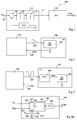
- Figure 1 illustrates an example of a sigma-delta ADC 100 comprising a sigma-delta modulator 102 and a decimation filter 104.
- the modulator 102 comprises a subtractor 106, which subtracts a feedback signal from the input signal voltage V in provided on an input line 107.
- the output of the subtractor 106 is coupled to an integrator 108, which integrates this signal and provides the result to a 1-bit quantization unit 110.
- the quantization unit 110 uses a single threshold value to provide a binary output, which is the sigma-delta modulated signal.
- This signal is provided on an output line 111, coupled to a digital to analog converter (DAC) 112.
- DAC 112 generates an analog level based on the sigma-delta modulated signal, and provides this analog level on the feedback line to the subtractor 106.
- DAC digital to analog converter
- the sigma-delta modulator 102 provides a stream of bits having a spectral power determined by the level of the input signal V in , wherein the higher the input signal, the higher the power and quantization noise.
- the output of the quantization unit 110 on line 111 is provided to the decimation filter 104, which filters the noise and down converts the high frequency bit stream into a high resolution digital code at the Nyquist rate. In particular, this involves applying an averaging filter function and a rate reduction function simultaneously to generate the high resolution digital code.
- Figure 2 shows an example of an integrated circuit 200 comprising the sigma-delta ADC 100 of Figure 1 , and external test equipment 202 for testing the ADC 100.
- the test equipment provides a high resolution analog test waveform on an input line 204 to the ADC 100, and receives the n-bit output on a line 206 from the ADC.
- the arrangement of Figure 2 is not a BIST solution, and has the drawback that the test equipment is necessarily complex in order to generate the high resolution analog waveform. Furthermore, for cost reasons, the number of test equipment 202 will generally be limited, and downloading to the test equipment the large number of n-bit digital values from the output of the converter 100 takes a relatively long time. Thus testing a large number of integrated circuits using this arrangement will be very time consuming.
- Figure 3 illustrates an alternative arrangement that has been proposed, in which an integrated circuit 300 comprises the sigma-delta ADC 100, and receives a binary test signal V BIN .
- the test equipment 302 generates a digital 1-bit signal on an input line 304 to the integrated circuit 300.
- the input line 304 is coupled to a DAC 306, which converts the digital signal into the binary test signal V BIN by substituting the logic high and logic low levels of the digital signal with desired voltage amplitudes.
- the use of a purely digital test signal does not necessitate an analog filter at the input of the sigma-delta ADC since the converter architecture rejects the high frequency noise contained in the bit stream.
- Figure 3 could be adapted to become a BIST solution if the digital test signal on line 304 is stored or generated on-chip, and the n-bit output of the sigma-delta ADC 100 analysed on-chip.
- Figure 4A illustrates a sigma-delta ADC 400 comprising a sigma-delta modulator 401 having input circuitry 402 and a modulation block 403.
- ADC 400 also comprises a decimation filter 404. Rather than an analogue or binary test signal, a ternary test signal is applied to the converter during a test mode.
- the input circuitry 402 provides to the rest of the modulation block 403, on a line 405, an analog input voltage V in during a normal mode of operation, or a ternary test signal during a test mode of operation.
- the input circuitry receives the analog input voltage V in on an input 406, and a digital test control signal D test at an input 407.
- the digital test control signal D test is used to generate the ternary test signal by controlling the selection between three test voltages to be applied to the input line 405.
- the three test voltages are voltage levels V A , V 0 , and V B , provided on lines 408, 410 and 412 to the input circuitry.
- Voltage levels V A and V B are for example positive and negative test voltage levels, and V 0 is a neutral voltage.
- test voltage levels V A and V B may for example have equal absolute magnitudes in the case of a differential implementation, as will be described in more detail below with reference to Figure 5 .
- the magnitude of test voltages V A and V B are for example chosen based on the desired amplitude of the test signal.
- the digital test control signal D test encodes, for example on two or three bit lines, the information indicating which of the three test voltage levels, V A , V 0 and V B , the ternary test signal is to have at any time.
- Figure 4B illustrates the input circuitry 402 of the sigma-delta modulator 401 of Figure 4A in more detail according to one embodiment.
- the input circuitry 402 for example comprises switching blocks 420, 422 and 424.
- Switching block 420 receives a binary signal D 1
- switching block 422 receives a binary signal D 0
- switching block 424 receives a binary signal D -1 .
- the binary signals D 1 , D 0 and D -1 form the digital test data signal D test of Figure 4A .
- the outputs of switches 420, 422, 424 are all coupled to line 405. Only one of the binary signals D 1 , D 0 and D -1 is asserted at any one time, indicating which of the three test voltage levels V A , V 0 and V B should be applied at that time to line 405.
- each of the switching blocks couples the corresponding voltage level V A , V 0 , V B to line 405 when the corresponding binary signal D 1 , D 0 , D -1 is asserted, for example by a logic "1".
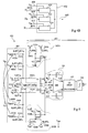
- Figure 5 illustrates the modulator 401 of Figure 4A in more detail according to one embodiment in which the converter is a second-order switched capacitor differential converter.
- the sigma-delta modulator 401 comprises, in addition to the input circuitry 402, an integrator 501, a feedback stage comprising digital to analog converters 502A and 502B, a sigma-delta modulator second stage 503, and a quantization unit 504.
- the integrator 501 comprises an operational amplifier 505 having differential inputs 506, 508 and differential outputs 510, 512, the output 510 being coupled to the input 506 via a capacitor C i + , and the output 512 being coupled to the input 508 via a capacitor C i - .
- the input 506 is coupled via a switch 516 and a sampling capacitor C s + to a line 405A, which is in turn coupled to the positive input of the integrator 501 via a switch 517A.
- the input 508 is coupled via a switch 518 and a sampling capacitor C s - to a line 405B, which is in turn coupled to the negative input of the integrator 501 via a switch 517B.
- a node 520 between switch 516 and capacitor C s + is coupled to a common mode voltage V cm , via a switch 521, and a node 522 between switch 518 and capacitor C s - is coupled to voltage V cm via a switch 523.
- the integrator 501 comprises switches 527A and 527B coupled between the inputs lines 405A, 405B respectively and voltage V cm .
- DAC 502A of the feedback stage comprises a switch 524A coupled between a high reference voltage V ref + and a node 525A, and a switch 526A coupled between a low reference voltage V ref - and the node 525A.
- Node 525A is also coupled to the node 520 of integrator 501 via a capacitor C dac + , and to voltage V cm via a switch 528A.
- DAC 502B comprises a switch 524B coupled between a high reference voltage V ref + and a node 525B, and a switch 526B coupled between a low reference voltage V ref - and node 525B.
- Node 525B is coupled to node 522 of integrator 501 via a capacitor C dac - and to voltage V cm via switch 528B.
- the input circuitry 402 comprises switches 532A and 532B coupled between a low test voltage V BIST - and the input lines 405A and 405B respectively, and switches 534A and 534B coupled between a high test voltage V BIST + and the input lines 405A and 405B respectively.
- the input circuitry 402 also comprises the switches 517A, 517B, 527A, 527B of the integrator 501, in that these switches are adapted to additionally receive control signals for controlling the test mode, as will be explained in more detail below.
- the input circuitry 402 could comprise separate switches to the switches 527A, 527B for coupling the lines 405A, 405B to the differential ground voltage.
- the differential outputs of the integrator 501 on lines 510 and 512 are coupled to corresponding inputs of the sigma-delta modulator second stage 503.
- This second stage 503 for example comprises a further integrator and DACs identical to integrator 501 and DACs 502A, 502B.
- the differential outputs of modulator 503 are coupled to corresponding inputs of the quantization unit 504, which provides the output signal S 0, 1 , which is the sigma-delta modulated signal.
- the common mode voltage V cm is the differential ground voltage.
- the test voltage level V A is generated by the voltage difference between V BIST- and V BIST+ , in other words it is equal to V BIST+ - V BIST- .
- the test voltage V B is generated by the voltage difference between VBIST+ and V BIST- , in other words it is equal to V BIST- - V BIST+ .
- test voltage levels V A , V 0 and V B could be generated based on only a single voltage level V BIST , and a common mode voltage V cm .
- the digital control signals to the various switches in Figure 5 comprise the following signals:
- the switches 516 and 518 of the integrator 501 are controlled by signal ⁇ 2 , while switches 521 and 523 are controlled by the signal ⁇ 1 .
- the switches 528A, 528B of the DACs 502A and 502B are controlled by the signal ⁇ 2 , while the switches 524A and 526A are conducting when both ⁇ 1 and S 0 are high, and switches 526A and 524B are conducting when both ⁇ 1 and S 1 are high.
- the switches 517A and 517B of the integrator 501 are each conducting when the signals ⁇ 1 and T 0 are high.
- the switches 532A and 534B of the input circuitry 402 are conducting when signals ⁇ 1 , T 1 , and D -1 are all high.
- the switches 534A and 532B of the input circuitry 402 are conducting when signals ⁇ 1 , T 1 , and D 1 are all high.
- the switches 536A and 536B of the integrator 501 are conducting when signal ⁇ 2 is high, or when signals ⁇ 1 , T 1 and D 0 are all high.
- the signal T 0 is high.
- the input voltages V in + , V in - are sampled to capacitors C s + , C s - , and at the same time, inverted feedback voltages are sampled by the DACs 502A, 502B onto the capacitors C dac + and C dac - respectively.
- the input lines 405A, 405B are grounded to the same common mode voltage V cm , and the inverted feedback voltages on capacitors C dac + and C dac - are added to the sampled voltage on capacitors C s + , C s - at the inputs 506, 508 of the operational amplifier 504. In this way, the feedback voltages are effectively subtracted from the input voltages before integration.
- the DACs 502A, 502B operate as in the normal mode, but the input circuitry 402 of the modulator 401 applies a ternary test voltage.
- the switches 527A and 527B are no longer just used for coupling the input lines 405A, 405B to ground during the integration phase, but also provide the differential zero test voltage V 0 during the sampling phase by coupling both lines 405A and 405B to the same voltage, in this case the common mode voltage V cm .
- the test voltages V A and V B are provided by the additional four switches 532A, 532B, 534A, 534B.
- the input lines 405A, 405B could simply be coupled to the inputs V in- and V in+ , which could be shortcircuited. In this case, only switches 517A, 517B will be activated when the voltage V 0 is to be applied.
- switches 532A,B and 534A,B could be coupled to the V in+ and V in- input nodes before the switches 517A and 517B, in other words to the input line 406 of Figure 4A .
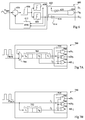
- Figure 6 illustrates an example of circuitry 600 for generating, based on an analog test signal V test , the digital test control signal D test , in this example comprising the three control signals D 1 , D 0 and D -1 used in the embodiment of Figure 5 .
- the circuitry 600 is for example implemented by an appropriate computer-aided tool separate to the chip containing the sigma-delta ADC to be tested, and the sequences of the signals D 1 , D 0 and D -1 may for example be stored in a memory embedded on-chip with the sigma-delta modulator to be tested, or stored to a memory of the test equipment such that it can be sent directly to the sigma-delta modulator to be tested via a low-cost test equipment during a testing phase.
- the circuitry 600 comprises a multi-bit sigma-delta modulator 602, for example provided by an ideal computer-aided simulation, comprising a subtractor 604, which subtracts a feedback voltage from the input voltage, and provides the result to an integrator 606.
- the integrator 606 provides the result to a pair of quantization units 608, 610, each having a different quantization level.
- the outputs of the quantization units 608, 610 are provided to a three-state DAC 612, which provides the feedback voltage to subtractor 604 based on these outputs.
- quantization unit 608 has a higher threshold than unit 610
- the unit 608 is used to determine the cut-off between when the differential zero test voltage V 0 and test voltage V A of the ternary test signal is applied
- the unit 610 is used to determine the cut-off between when the differential zero test voltage V 0 and test voltage V B of the ternary test signal are applied.
- a logic block 614 receives the outputs from the quantization units 608, 610, and generates the three control signals D 1 , D 0 and D -1 based on these outputs.
- the signal D 1 is equal to the output of quantization unit 608, D -1 is equal to the inverse of the output of quantization unit 608 provided by an inverter 616, and D 0 is equal to the AND function, provided by an AND gate 618, between the inverse of the output of quantization unit 608 provided by an inverter 620, and the output of quantization unit 610.
- circuitry 600 could be use to generate a binary test signal, provided to the on-chip circuitry of Figures 7A or 7B , which will now be described.
- Figures 7A and 7B illustrate alternative examples of circuitry for generating the digital test control signals D 1 , D 0 and D -1 , in this example based on a binary test signal D BIN , which is for example stored in a memory on the chip containing the sigma-delta ADC to be tested, or supplied by a low-cost test equipment during a test phase.
- the digital test control signal is generated by adding the values of the binary test signal D BIN to a delayed version of the binary test signal.
- a register 702 is comprised of flip-flops r 1 to r n , where n is equal to the number N of values in the binary test sequence.
- the values are initially loaded to the register 702 via a multiplexer 704, which is initially controlled to select the binary test signal D BIN .
- the binary sequence of the binary test signal D BIN for example has a length of N samples at the frequency F clk .
- the frequency Fclk is for example the same frequency as the clocking frequency of the sigma-delta ADC under test, or at a different frequency.
- the multiplexer 704 is controlled to select a feedback from the output of the register 702, such that register 702 becomes a linear feedback shift register (LFSR) that circulates the binary test sequence.
- LFSR linear feedback shift register
- the digital test control signals D 1 , D -1 and D 0 are generated by a logic block 705 based on the data value J 1 in flip-flop r 1 at the output of the register, and on the data value J 2 in a flip-flop r ⁇ , which is one or more flip-flops before flip-flop r 1 .
- the value of ⁇ is for example equal or greater than 1.
- Logic block 705 comprises an AND gate 706, which generates signal D 1 by performing the AND function on signals J 1 and J 2 , an XOR gate 708, which generates the signal D 0 by performing the XOR function on signals J 1 and J 2 , and a NOR gate 710, which generates the signal D -1 by performing a NOR function on the signals J 1 and J 2 .
- signal D 1 is high when J 1 and J 2 are both high
- signal D -1 is high when J 1 and J 2 are both low
- signal D 0 is high if only one or the other of the signals J 1 , J 2 is high.
- Figure 7B illustrates an alternative embodiment 752 in which the binary test signal D BIN directly provides the signal J 1 , and the signal J 2 is provided by the output of a register 752 having only ⁇ registers r 1 to r ⁇ .
- the same logic block 705 as in Figure 7A is for example used to generate the signals D 1 , D 0 and D -1 respectively based on J 1 and J 2 .
- An advantage of the embodiment of Figure 7B is that the register 752 is smaller than the register 702 of Figure 7A , and thus the area overhead is lower.
- the binary sequence is supplied periodically for example by repeatedly sending it from the memory of an external low-cost test equipment, or by generating it repeatedly by a digital resonator.
- the amplitude A T of the ternary signal is reduced according to a cosine function of the delay ⁇ , and the phase difference between the binary and ternary signals varies linearly with ⁇ .
- the ternary signal can be shown to have almost half the quantization noise power with respect to its binary counter part.
- Figure 8 illustrates and example of the binary signals J 1 and J 2 of Figure 7A or 7B , and the corresponding digital test control signals D 1 , D 0 and D -1 , and an example of a resulting ternary test signal generated based on these control signals, and having the test voltage levels V A , V B and V 0 .
- FIG. 9 illustrates an integrated circuit 900 comprising a sigma-delta ADC and BIST.
- a sigma-delta modulator 902 which for example comprises the modulator 401 with input circuitry 402 of Figure 5 , receives an analog signal on an input line 904, and a digital test control signal D test on an input line 906.
- the modulator 902 also receives a timing signal F clk used for generating the phase signals ⁇ 1 and ⁇ 2 of Figure 5 , and the signal T indicating the activation of the test mode.
- a block 908 provides the reference voltage V ref + and V ref -, and the test voltages V BIST+ and V BIST- of Figure 5 .
- the 1-bit output of the modulator 902 is provided to a two-input multiplexer 910, the other input being provided by a control block 912 via a delay block 914.
- Control block 912 in this example corresponds to the circuitry 700 of Figure 7A , and comprises the register 702, multiplexer 704, and logic block 705, although in alternative embodiments other circuit arrangements could be used.
- the multiplexer 704 has an input coupled to an on-chip pin access 916 for loading a binary sequence into the register 702 for example from an external test equipment (not shown).
- the delay block 914 receives the signal J 1 from the output of the register 702.
- the output of multiplexer 910 is coupled to a decimation filter 920, which also receives the timing signal F clk , and which provides an output on an output line 922 of n+3 bits in parallel for generating a high resolution reference signal.
- the output line 922 is coupled to a reference memory 924, which stores a reference sequence, and a response memory 926, which stores a response sequence.
- the reference and response sequences are compared by a block 928, which provides a result on an output line 930.
- the binary test sequence is loaded into the register 702. It is then provided to the delay block 914, which introduces a delay Z -(L+ ⁇ ) , where L is the order of the sigma-delta converter, for example equal to 2.
- L is the order of the sigma-delta converter, for example equal to 2.
- the block 914 introduces a three-cycle delay, such that the code values at the output of decimation filter are synchronised with the corresponding output code values of the sigma-delta modulator 902 under test.
- the digital multiplexer 910 is controlled to couple the output of the delay block 914 to the decimation filter 920.
- the values, after filtering by the decimation filter 920, from the delay element 914 are stored in the reference memory 924.
- the same binary test sequence loaded into the register 702 is provided to the sigma-delta modulator 902 under test.
- the digital multiplexer 910 is controlled to couple the output of the ADC 902 to the decimation filter 920, and the values, after filtering by the decimation filter 920, from the converter 902 are stored in the response memory 926.
- the analysis block 928 then analyses the sequences in memories 924 and 926 to determine whether the test is successful, for example using a sine wave fitting algorithm.
- a sine wave fitting algorithm is for example discussed in the publication titled " A Stereo Audio ⁇ ADC Architecture with Embedded SNDR Self-Test", L.Rolindez et al.
- SNR signal-to-noise-ratio
- SNDR signal-to-noise-and-distortion-ratio
- the delay parameter ⁇ is for example selected to have a particular optimized value for each amplitude value of the ternary test signal.
- the ternary test signal ideally has a high SNDR (signal-to-noise-and-distortion-ratio) and a low power.
- the SNDR and power for given values of ⁇ and the amplitude can be determined, and used to select the optimal value of ⁇ .
- An advantage of embodiments described herein in which a ternary test signal is applied to test a sigma-delta ADC is that such a signal has a reduced quantization noise and a better resolution of the test when compared to a binary signal. This allows dynamic performance measurements close to the full input dynamic range of the sigma-delta ADC under test. Furthermore, no filter is needed at the input of the sigma-delta ADC to filter the ternary signal as the converter architecture rejects the high frequency noise present in the ternary stream. Also, the ternary test sequence may be generated or stored on-chip, thereby permitting a full BIST solution.
- the digital test control signal D test for the ternary test stream is generated based on a binary test signal in a simple fashion.
- the amplitude and phase of the ternary test signal can be controlled in a simple manner.
- test signal having three states better emphasizes non-linearity in the integrator stage than a binary test signal, due to the extra state.
- ternary test signal could be generated based on a binary test signal, or by other means.
- the three signals D 1 , D 0 and D -1 could be replaced by a 2-bit signal for example having the value "00" when the low test voltage V BIST- is to be selected, the value “01” or “10” when the common mode test voltage V cm is to be selected, or the value "11" when the high test signal V BIST+ is to be selected.
- Figure 5 is a second-order converter, it will be apparent to those skilled in the art that the principles described herein could be applied to any sigma-delta modulator architecture, having any number of stages, any feedback DAC architecture, and producing any number of bits.
Landscapes
- Engineering & Computer Science (AREA)
- Theoretical Computer Science (AREA)
- Compression, Expansion, Code Conversion, And Decoders (AREA)
- Analogue/Digital Conversion (AREA)
Claims (18)
- Ein sigma-delta geschalteter Kondensator analog zu digital Konverter (ADC), wobei der Konverter Folgendes aufweist:einen Eingangsleitung (405) zum Empfangen eines zu konvertierenden Signals; dadurch gekennzeichnet, dass er Folgendes aufweist:einen Umschalt-Schaltkreis (402), der geeignet ist, während eines Testmodus des sigma-delta ADCs, ein ternäres Testsignal an die Eingangsleitung (405) anzulegen, durch periodisches Auswählen, basierend auf einem digitalen Teststeuersignal (Dtest), einer von einer ersten, zweiten oder dritten Testspannung (VA, V0, VB), die an die Eingangsleitung (405) anzulegen ist.
- Der sigma-delta ADC nach Anspruch 1, wobei der ADC ferner Folgendes aufweist:erste, zweite und dritte Eingänge (408, 410, 412) um entsprechende erste, zweite und dritte Testspannungen (VA, V0, VB) zu empfangen.
- Der sigma-delta ADC nach Anspruch 2, wobei der sigma-delta ADC ein differentieller Konverter ist, wobei die erste, zweite und dritte Testspannung (VA, V0, VB) differentielle Spannungen sind und wobei jeder der ersten, zweiten und dritten Eingänge (408, 410, 412) ein Paar von differentiellen Eingangsanschlüssen (408A, 408B, 410A, 410B, 412A, 412B) aufweist, über die die erste, zweite und dritte differentielle Testspannung (VA, V0, VB) entsprechend angelegt wird.
- Der sigma-delta ADC nach Anspruch 2 oder 3, wobei der ADC ferner einen vierten Eingang (406) aufweist zum Empfangen eines analogen Eingangssignals (Vin), wobei der Umschalt-Schaltkreis (402) derart angeordnet ist, dass er das analoge Eingangssignal (Vin) an die Eingangsleitung (405) während eines Normalmodus des sigma-delta ADC anlegt.
- Der sigma-delta ADC nach einem der Ansprüche 2 bis 4, wobei der Umschalt-Schaltkreis (402) einen ersten Schalter (420, 534A, B) aufweist, der zwischen den ersten Eingang (408) und die Eingangsleitung (405) gekoppelt ist, einen zweiten Schalter (422, 517A, B, 527A, B) aufweist, der zwischen den zweiten Eingang (410) und die Eingangsleitung (405) gekoppelt ist, und einen dritten Schalter (424, 532A, B) aufweist, der zwischen den dritten Eingang (412) und die Eingangsleitung (405) gekoppelt ist, wobei das digitale Teststeuersignal (Dtest) erste, zweite und dritte Steuersignale (D-1, D0, D1) aufweist, die geeignet sind den ersten, zweiten und dritten Schalter entsprechend zu steuern.
- Der sigma-delta ADC nach Anspruch 5, wobei die erste Testspannung (VA) einer Spannungsdifferenz zwischen einem ersten Spannungspegel (VBIST+) und einem zweiten Spannungspegel (VBIST-) entspricht, die an die differentiellen Eingänge (408A, 408B) des ersten Schalters angelegt werden, und wobei die dritte Testspannung (VB) einer Spannungsdifferenz zwischen dem zweiten Spannungspegel und dem ersten Spannungspegel entspricht, die an die differentiellen Eingänge (412A, 412B) des zweiten Schalters angelegt werden.
- Der sigma-delta ADC nach Anspruch 6, wobei der erste Spannungspegel (VBIST+) gleich einer positiven Referenzspannung (Vref+) ist, die an einen ersten Rückmeldungsblock (502A) des sigma-delta ADCs angelegt wird, und wobei der zweite Spannungspegel (VBIST-) gleich einer negativen Referenzspannung (Vref-) ist, die an einen zweiten Rückmeldungsblock (502B) des sigma-delta ADCs angelegt wird.
- Der sigma-delta ADC nach einem der Ansprüche 1 bis 7, wobei die zweite Testspannung (V0) eine differentielle Null Spannung ist, die an beide Anschlüsse eines Paars von Samplingkondensatoren (Cs +, Cs -) des sigma-delta ADCs angelegt wird.
- Ein integrierter Schaltkreis, wobei der Schaltkreis den sigma-delta ADC nach einem der Ansprüche 1 bis 8 aufweist und Steuerelektronik (600, 700, 750) die geeignet ist das digitale Teststeuersignal (Dtest) zu erzeugen.
- Der integrierte Schaltkreis nach Anspruch 9, wobei die Steuerelektronik (600, 700, 750) einen sigma-delta Modulator (602) aufweist, zum Anlegen einer sigma-delta Modulation an ein analoges Testsignal (Vtest), wobei der sigma-delta Modulator zwei Komparatoren (608, 610) aufweist zum Detektieren, wann der Wert des analogen Testsignals (Vtest) in einem von drei Bereichen ist.
- Der integrierte Schaltkreis nach Anspruch 9, wobei die Steuerelektronik (600, 700, 750) geeignet ist das digitale Teststeuersignal (Dtest) basierend auf einem binären Testsignal (DBIN) zu erzeugen.
- Der integrierte Schaltkreis nach Anspruch 11, wobei die Steuerelektronik (600, 700, 750) ein Verzögerungselement (702, 752) aufweist, das geeignet ist eine verzögerte Version des binären Testsignals (DBIN) zu erzeugen, und Logik (706, 708, 710) zum Erzeugen des digitalen Teststeuersignals (Dtest) basierend auf dem binären Testsignal (DBIN) und der verzögerten Version des binären Testsignals.
- Der integrierte Schaltkreis nach Anspruch 12, wobei das Verzögerungselement (702) ein lineares Rückmeldungsschieberegister ist, das geeignet ist die binäre Sequenz des binären Testsignals (DBIN) zu speichern.
- Der integrierte Schaltkreis nach einem der Ansprüche 11 oder 12, wobei der Schaltkreis ferner einen Speicher (916) aufweist, der das binäre Testsignal (DBIN) speichert.
- Ein Verfahren zum Testen eines sigma-delta geschalteten Kondensator analog zu digital Konverters (ADC), dadurch gekennzeichnet, dass es das Anlegen, während eines Testmodus, eines ternären Testsignals an eine Eingangsleitung (405) des sigma-delta ADCs aufweist, durch periodisches Auswählen, basierend auf einem digitalen Teststeuersignal (Dtest), einer von einer ersten, zweiten oder dritten Testspannung (VA, V0, VB), die an die Eingangsleitung anzulegen ist.
- Das Verfahren nach Anspruch 15, wobei der sigma-delta ADC ein differentieller Konverter ist, und das ternäre Testsignal erste, zweite und dritte differentielle Spannungspegel (VA, V0, VB) aufweist.
- Das Verfahren nach Anspruch 16, wobei der zweite differentielle Spannungspegel (V0) eine differentielle Null Spannung ist.
- Das Verfahren nach Anspruch 15 oder 16, wobei das digitale Teststeuersignal erzeugt wird, basierend auf einem des Folgenden:einem binären Testsignal (DBIN), undeinem analogen Testsignal (Vtest).
Applications Claiming Priority (2)
| Application Number | Priority Date | Filing Date | Title |
|---|---|---|---|
| FR1002741A FR2962273B1 (fr) | 2010-06-30 | 2010-06-30 | Convertisseur analogique-numerique sigma-delta muni d'un circuit de test |
| PCT/EP2011/060863 WO2012001019A1 (en) | 2010-06-30 | 2011-06-28 | Sigma-delta adc with test circuitry |
Publications (2)
| Publication Number | Publication Date |
|---|---|
| EP2589153A1 EP2589153A1 (de) | 2013-05-08 |
| EP2589153B1 true EP2589153B1 (de) | 2016-06-15 |
Family
ID=43536652
Family Applications (1)
| Application Number | Title | Priority Date | Filing Date |
|---|---|---|---|
| EP11727990.1A Not-in-force EP2589153B1 (de) | 2010-06-30 | 2011-06-28 | Sigma-delta-adc mit prüfschaltung |
Country Status (5)
| Country | Link |
|---|---|
| US (1) | US8830098B2 (de) |
| EP (1) | EP2589153B1 (de) |
| CN (1) | CN103201956B (de) |
| FR (1) | FR2962273B1 (de) |
| WO (1) | WO2012001019A1 (de) |
Families Citing this family (12)
| Publication number | Priority date | Publication date | Assignee | Title |
|---|---|---|---|---|
| DE102012111586B4 (de) * | 2012-11-29 | 2014-10-30 | Infineon Technologies Ag | Verfahren und Vorrichtungen zum Testen von Analog-Digital-Wandlern |
| CN103995169B (zh) * | 2014-04-25 | 2016-07-20 | 嘉兴泰鼎光电集成电路有限公司 | 芯片内部节点电压的测试电路 |
| US9401728B2 (en) * | 2014-12-16 | 2016-07-26 | Freescale Semiconductor, Inc. | Test signal generator for sigma-delta ADC |
| US9350381B1 (en) * | 2014-12-16 | 2016-05-24 | Freescale Semiconductor Inc. | Circuit generating an analog signal using a part of a sigma-delta ADC |
| CN104963676A (zh) * | 2015-06-25 | 2015-10-07 | 中国石油天然气股份有限公司 | 一种钻井防碰预警装置及方法 |
| US11106705B2 (en) | 2016-04-20 | 2021-08-31 | Zestfinance, Inc. | Systems and methods for parsing opaque data |
| CN107544020B (zh) * | 2016-06-29 | 2021-02-05 | 恩智浦美国有限公司 | 用于∑-△调制器的内建自测试电路 |
| US9780803B1 (en) * | 2016-09-15 | 2017-10-03 | Stmicroelectronics International N.V. | Apparatus for built-in self-test (BIST) of a Nyquist rate analog-to-digital converter (ADC) circuit |
| US12000886B2 (en) * | 2017-12-04 | 2024-06-04 | Aktiebolaget Skf | Self-test circuit and a method of checking the integrity of a signal through a signal path |
| US10461771B2 (en) * | 2018-03-20 | 2019-10-29 | Texas Instruments Incorporated | Sigma-delta analog-to-digital converter with multiple counters |
| CN112737584B (zh) * | 2020-12-31 | 2023-08-01 | 中国电子科技集团公司第十四研究所 | 一种片内全集成电容失配校准电路 |
| CN112630626B (zh) * | 2021-03-05 | 2021-10-22 | 光梓信息科技(上海)有限公司 | 片上自测试系统及方法 |
Family Cites Families (8)
| Publication number | Priority date | Publication date | Assignee | Title |
|---|---|---|---|---|
| GB2349756B (en) * | 1999-05-06 | 2003-05-14 | Sony Uk Ltd | Signal processors |
| US6907374B1 (en) * | 2003-03-19 | 2005-06-14 | Zilog, Inc. | Self-calibrating sigma-delta analog-to-digital converter |
| KR100513384B1 (ko) * | 2003-08-04 | 2005-09-07 | 삼성전자주식회사 | 신호 처리장치의 테스트 장치 및 테스트 방법 |
| US7062401B1 (en) * | 2005-01-11 | 2006-06-13 | Lsi Logic Corporation | Low circuit overhead built in self test for oversampled ADC's |
| TWI270254B (en) * | 2005-09-16 | 2007-01-01 | Univ Nat Chiao Tung | Reprogrammable switched-capacitor input circuit for receiving digital test stimulus signal in analog test |
| US7773020B2 (en) * | 2007-02-15 | 2010-08-10 | Analog Devices, Inc. | Analog to digital converter |
| US7495589B1 (en) * | 2007-09-17 | 2009-02-24 | Texas Instruments Incorporated | Circuit and method for gain error correction in ADC |
| US7741981B1 (en) * | 2008-12-30 | 2010-06-22 | Hong Kong Applied Science And Technology Research Institute Co., Ltd. | Dual-use comparator/op amp for use as both a successive-approximation ADC and DAC |
-
2010
- 2010-06-30 FR FR1002741A patent/FR2962273B1/fr not_active Expired - Fee Related
-
2011
- 2011-06-28 CN CN201180041389.9A patent/CN103201956B/zh not_active Expired - Fee Related
- 2011-06-28 US US13/807,632 patent/US8830098B2/en not_active Expired - Fee Related
- 2011-06-28 EP EP11727990.1A patent/EP2589153B1/de not_active Not-in-force
- 2011-06-28 WO PCT/EP2011/060863 patent/WO2012001019A1/en not_active Ceased
Non-Patent Citations (1)
| Title |
|---|
| None * |
Also Published As
| Publication number | Publication date |
|---|---|
| FR2962273A1 (fr) | 2012-01-06 |
| WO2012001019A1 (en) | 2012-01-05 |
| CN103201956B (zh) | 2016-04-27 |
| FR2962273B1 (fr) | 2012-07-27 |
| CN103201956A (zh) | 2013-07-10 |
| US8830098B2 (en) | 2014-09-09 |
| US20130201046A1 (en) | 2013-08-08 |
| EP2589153A1 (de) | 2013-05-08 |
Similar Documents
| Publication | Publication Date | Title |
|---|---|---|
| US8830098B2 (en) | Sigma-delta ADC with test circuitry | |
| CN106888018B (zh) | Dac时序失配误差的数字测量 | |
| EP1819044B1 (de) | Mehrpegelquantisierer mit Current-Mode-DEM-Schaltmatrizen und separater DEM-Entscheidungslogik für einen Multibit-Sigma-Delta-Modulator | |
| EP1418674B1 (de) | Wandler, Schaltung und Verfahren zur Kompensation von Ungenauigkeiten in eienem Sigma Delta Wandler | |
| US9401728B2 (en) | Test signal generator for sigma-delta ADC | |
| CN107835020B (zh) | 用于内置自测尼奎斯特速率模数转换器电路的设备 | |
| US7760121B2 (en) | Dual data weighted average dynamic element matching in analog-to-digital converters | |
| JP4543209B2 (ja) | デジタルディザを用いる多段変換器 | |
| US11251807B1 (en) | Wide bandwidth ADC with inherent anti-aliasing and high DC precision | |
| US6111529A (en) | Accurate gain calibration of analog to digital converters | |
| US5905453A (en) | Dithered sigma delta modulator having programmable full scale range adjustment | |
| US20160173121A1 (en) | Circuit generating an analog signal using a part of a sigma-delta adc | |
| US10056916B2 (en) | Analog/digital conversion with analog filtering | |
| US10897232B2 (en) | Multi-level capacitive digital-to-analog converter for use in a sigma-delta modulator | |
| JP4940101B2 (ja) | Δςデータ変換装置およびδςデータ変換装置の検査方法 | |
| US8836549B2 (en) | Use of logic circuit embedded into comparator for foreground offset cancellation | |
| JP2009534874A (ja) | オフセットを用いるシグマ−デルタ変調 | |
| US6903672B1 (en) | Apparatus for and method of performing an analog to digital conversion | |
| WO2007009912A1 (en) | Method for testing analog-to-digital converters | |
| CN120825170A (zh) | 双模式可切换的逐次逼近模数转换器及切换方法 | |
| Delic-Ibukic et al. | Continuous gain calibration of parallel delta sigma A/D converters | |
| Rivoir | Low-cost analog signal generation using a pulse-density modulated digital ATE channel | |
| Ankur et al. | A novel on-chip mismatch measurement technique for Nyquist rate ADCs | |
| Loumeau et al. | A time-interleaved chopper-stabilized Delta-Sigma analog to digital converter | |
| Ting et al. | Oscillator-based reconfigurable sinusoidal signal generator for ADC BIST |
Legal Events
| Date | Code | Title | Description |
|---|---|---|---|
| PUAI | Public reference made under article 153(3) epc to a published international application that has entered the european phase |
Free format text: ORIGINAL CODE: 0009012 |
|
| 17P | Request for examination filed |
Effective date: 20130129 |
|
| AK | Designated contracting states |
Kind code of ref document: A1 Designated state(s): AL AT BE BG CH CY CZ DE DK EE ES FI FR GB GR HR HU IE IS IT LI LT LU LV MC MK MT NL NO PL PT RO RS SE SI SK SM TR |
|
| RIN1 | Information on inventor provided before grant (corrected) |
Inventor name: STRATIGOPOULOS, HARALAMPOS Inventor name: MIR, SALVADOR Inventor name: DUBOIS, MATTHIEU |
|
| DAX | Request for extension of the european patent (deleted) | ||
| 17Q | First examination report despatched |
Effective date: 20150504 |
|
| RAP1 | Party data changed (applicant data changed or rights of an application transferred) |
Owner name: STMICROELECTRONICS INTERNATIONAL N.V. |
|
| GRAP | Despatch of communication of intention to grant a patent |
Free format text: ORIGINAL CODE: EPIDOSNIGR1 |
|
| INTG | Intention to grant announced |
Effective date: 20160322 |
|
| GRAS | Grant fee paid |
Free format text: ORIGINAL CODE: EPIDOSNIGR3 |
|
| GRAA | (expected) grant |
Free format text: ORIGINAL CODE: 0009210 |
|
| AK | Designated contracting states |
Kind code of ref document: B1 Designated state(s): AL AT BE BG CH CY CZ DE DK EE ES FI FR GB GR HR HU IE IS IT LI LT LU LV MC MK MT NL NO PL PT RO RS SE SI SK SM TR |
|
| REG | Reference to a national code |
Ref country code: CH Ref legal event code: EP Ref country code: GB Ref legal event code: FG4D |
|
| REG | Reference to a national code |
Ref country code: FR Ref legal event code: PLFP Year of fee payment: 6 |
|
| REG | Reference to a national code |
Ref country code: IE Ref legal event code: FG4D |
|
| REG | Reference to a national code |
Ref country code: AT Ref legal event code: REF Ref document number: 806966 Country of ref document: AT Kind code of ref document: T Effective date: 20160715 |
|
| REG | Reference to a national code |
Ref country code: DE Ref legal event code: R096 Ref document number: 602011027437 Country of ref document: DE |
|
| REG | Reference to a national code |
Ref country code: LT Ref legal event code: MG4D |
|
| REG | Reference to a national code |
Ref country code: NL Ref legal event code: MP Effective date: 20160615 |
|
| PG25 | Lapsed in a contracting state [announced via postgrant information from national office to epo] |
Ref country code: FI Free format text: LAPSE BECAUSE OF FAILURE TO SUBMIT A TRANSLATION OF THE DESCRIPTION OR TO PAY THE FEE WITHIN THE PRESCRIBED TIME-LIMIT Effective date: 20160615 Ref country code: LT Free format text: LAPSE BECAUSE OF FAILURE TO SUBMIT A TRANSLATION OF THE DESCRIPTION OR TO PAY THE FEE WITHIN THE PRESCRIBED TIME-LIMIT Effective date: 20160615 Ref country code: NO Free format text: LAPSE BECAUSE OF FAILURE TO SUBMIT A TRANSLATION OF THE DESCRIPTION OR TO PAY THE FEE WITHIN THE PRESCRIBED TIME-LIMIT Effective date: 20160915 |
|
| REG | Reference to a national code |
Ref country code: AT Ref legal event code: MK05 Ref document number: 806966 Country of ref document: AT Kind code of ref document: T Effective date: 20160615 |
|
| PG25 | Lapsed in a contracting state [announced via postgrant information from national office to epo] |
Ref country code: SE Free format text: LAPSE BECAUSE OF FAILURE TO SUBMIT A TRANSLATION OF THE DESCRIPTION OR TO PAY THE FEE WITHIN THE PRESCRIBED TIME-LIMIT Effective date: 20160615 Ref country code: NL Free format text: LAPSE BECAUSE OF FAILURE TO SUBMIT A TRANSLATION OF THE DESCRIPTION OR TO PAY THE FEE WITHIN THE PRESCRIBED TIME-LIMIT Effective date: 20160615 Ref country code: HR Free format text: LAPSE BECAUSE OF FAILURE TO SUBMIT A TRANSLATION OF THE DESCRIPTION OR TO PAY THE FEE WITHIN THE PRESCRIBED TIME-LIMIT Effective date: 20160615 Ref country code: LV Free format text: LAPSE BECAUSE OF FAILURE TO SUBMIT A TRANSLATION OF THE DESCRIPTION OR TO PAY THE FEE WITHIN THE PRESCRIBED TIME-LIMIT Effective date: 20160615 Ref country code: RS Free format text: LAPSE BECAUSE OF FAILURE TO SUBMIT A TRANSLATION OF THE DESCRIPTION OR TO PAY THE FEE WITHIN THE PRESCRIBED TIME-LIMIT Effective date: 20160615 Ref country code: GR Free format text: LAPSE BECAUSE OF FAILURE TO SUBMIT A TRANSLATION OF THE DESCRIPTION OR TO PAY THE FEE WITHIN THE PRESCRIBED TIME-LIMIT Effective date: 20160916 |
|
| PG25 | Lapsed in a contracting state [announced via postgrant information from national office to epo] |
Ref country code: BE Free format text: LAPSE BECAUSE OF NON-PAYMENT OF DUE FEES Effective date: 20160630 |
|
| PG25 | Lapsed in a contracting state [announced via postgrant information from national office to epo] |
Ref country code: SK Free format text: LAPSE BECAUSE OF FAILURE TO SUBMIT A TRANSLATION OF THE DESCRIPTION OR TO PAY THE FEE WITHIN THE PRESCRIBED TIME-LIMIT Effective date: 20160615 Ref country code: IS Free format text: LAPSE BECAUSE OF FAILURE TO SUBMIT A TRANSLATION OF THE DESCRIPTION OR TO PAY THE FEE WITHIN THE PRESCRIBED TIME-LIMIT Effective date: 20161015 Ref country code: RO Free format text: LAPSE BECAUSE OF FAILURE TO SUBMIT A TRANSLATION OF THE DESCRIPTION OR TO PAY THE FEE WITHIN THE PRESCRIBED TIME-LIMIT Effective date: 20160615 Ref country code: CZ Free format text: LAPSE BECAUSE OF FAILURE TO SUBMIT A TRANSLATION OF THE DESCRIPTION OR TO PAY THE FEE WITHIN THE PRESCRIBED TIME-LIMIT Effective date: 20160615 Ref country code: IT Free format text: LAPSE BECAUSE OF FAILURE TO SUBMIT A TRANSLATION OF THE DESCRIPTION OR TO PAY THE FEE WITHIN THE PRESCRIBED TIME-LIMIT Effective date: 20160615 Ref country code: EE Free format text: LAPSE BECAUSE OF FAILURE TO SUBMIT A TRANSLATION OF THE DESCRIPTION OR TO PAY THE FEE WITHIN THE PRESCRIBED TIME-LIMIT Effective date: 20160615 |
|
| REG | Reference to a national code |
Ref country code: CH Ref legal event code: PL |
|
| PG25 | Lapsed in a contracting state [announced via postgrant information from national office to epo] |
Ref country code: PT Free format text: LAPSE BECAUSE OF FAILURE TO SUBMIT A TRANSLATION OF THE DESCRIPTION OR TO PAY THE FEE WITHIN THE PRESCRIBED TIME-LIMIT Effective date: 20161017 Ref country code: PL Free format text: LAPSE BECAUSE OF FAILURE TO SUBMIT A TRANSLATION OF THE DESCRIPTION OR TO PAY THE FEE WITHIN THE PRESCRIBED TIME-LIMIT Effective date: 20160615 Ref country code: ES Free format text: LAPSE BECAUSE OF FAILURE TO SUBMIT A TRANSLATION OF THE DESCRIPTION OR TO PAY THE FEE WITHIN THE PRESCRIBED TIME-LIMIT Effective date: 20160615 Ref country code: BE Free format text: LAPSE BECAUSE OF FAILURE TO SUBMIT A TRANSLATION OF THE DESCRIPTION OR TO PAY THE FEE WITHIN THE PRESCRIBED TIME-LIMIT Effective date: 20160615 Ref country code: SM Free format text: LAPSE BECAUSE OF FAILURE TO SUBMIT A TRANSLATION OF THE DESCRIPTION OR TO PAY THE FEE WITHIN THE PRESCRIBED TIME-LIMIT Effective date: 20160615 Ref country code: AT Free format text: LAPSE BECAUSE OF FAILURE TO SUBMIT A TRANSLATION OF THE DESCRIPTION OR TO PAY THE FEE WITHIN THE PRESCRIBED TIME-LIMIT Effective date: 20160615 |
|
| REG | Reference to a national code |
Ref country code: DE Ref legal event code: R097 Ref document number: 602011027437 Country of ref document: DE |
|
| REG | Reference to a national code |
Ref country code: IE Ref legal event code: MM4A |
|
| PG25 | Lapsed in a contracting state [announced via postgrant information from national office to epo] |
Ref country code: MC Free format text: LAPSE BECAUSE OF FAILURE TO SUBMIT A TRANSLATION OF THE DESCRIPTION OR TO PAY THE FEE WITHIN THE PRESCRIBED TIME-LIMIT Effective date: 20160615 |
|
| PLBE | No opposition filed within time limit |
Free format text: ORIGINAL CODE: 0009261 |
|
| STAA | Information on the status of an ep patent application or granted ep patent |
Free format text: STATUS: NO OPPOSITION FILED WITHIN TIME LIMIT |
|
| PG25 | Lapsed in a contracting state [announced via postgrant information from national office to epo] |
Ref country code: LI Free format text: LAPSE BECAUSE OF NON-PAYMENT OF DUE FEES Effective date: 20160630 Ref country code: CH Free format text: LAPSE BECAUSE OF NON-PAYMENT OF DUE FEES Effective date: 20160630 |
|
| REG | Reference to a national code |
Ref country code: FR Ref legal event code: PLFP Year of fee payment: 7 |
|
| 26N | No opposition filed |
Effective date: 20170316 |
|
| PG25 | Lapsed in a contracting state [announced via postgrant information from national office to epo] |
Ref country code: IE Free format text: LAPSE BECAUSE OF NON-PAYMENT OF DUE FEES Effective date: 20160628 Ref country code: DK Free format text: LAPSE BECAUSE OF FAILURE TO SUBMIT A TRANSLATION OF THE DESCRIPTION OR TO PAY THE FEE WITHIN THE PRESCRIBED TIME-LIMIT Effective date: 20160615 |
|
| PG25 | Lapsed in a contracting state [announced via postgrant information from national office to epo] |
Ref country code: SI Free format text: LAPSE BECAUSE OF FAILURE TO SUBMIT A TRANSLATION OF THE DESCRIPTION OR TO PAY THE FEE WITHIN THE PRESCRIBED TIME-LIMIT Effective date: 20160615 |
|
| REG | Reference to a national code |
Ref country code: FR Ref legal event code: PLFP Year of fee payment: 8 |
|
| PG25 | Lapsed in a contracting state [announced via postgrant information from national office to epo] |
Ref country code: CY Free format text: LAPSE BECAUSE OF FAILURE TO SUBMIT A TRANSLATION OF THE DESCRIPTION OR TO PAY THE FEE WITHIN THE PRESCRIBED TIME-LIMIT Effective date: 20160615 Ref country code: HU Free format text: LAPSE BECAUSE OF FAILURE TO SUBMIT A TRANSLATION OF THE DESCRIPTION OR TO PAY THE FEE WITHIN THE PRESCRIBED TIME-LIMIT; INVALID AB INITIO Effective date: 20110628 |
|
| PG25 | Lapsed in a contracting state [announced via postgrant information from national office to epo] |
Ref country code: MK Free format text: LAPSE BECAUSE OF FAILURE TO SUBMIT A TRANSLATION OF THE DESCRIPTION OR TO PAY THE FEE WITHIN THE PRESCRIBED TIME-LIMIT Effective date: 20160615 Ref country code: TR Free format text: LAPSE BECAUSE OF FAILURE TO SUBMIT A TRANSLATION OF THE DESCRIPTION OR TO PAY THE FEE WITHIN THE PRESCRIBED TIME-LIMIT Effective date: 20160615 Ref country code: LU Free format text: LAPSE BECAUSE OF NON-PAYMENT OF DUE FEES Effective date: 20160628 Ref country code: MT Free format text: LAPSE BECAUSE OF NON-PAYMENT OF DUE FEES Effective date: 20160630 |
|
| PG25 | Lapsed in a contracting state [announced via postgrant information from national office to epo] |
Ref country code: BG Free format text: LAPSE BECAUSE OF FAILURE TO SUBMIT A TRANSLATION OF THE DESCRIPTION OR TO PAY THE FEE WITHIN THE PRESCRIBED TIME-LIMIT Effective date: 20160615 |
|
| PG25 | Lapsed in a contracting state [announced via postgrant information from national office to epo] |
Ref country code: AL Free format text: LAPSE BECAUSE OF FAILURE TO SUBMIT A TRANSLATION OF THE DESCRIPTION OR TO PAY THE FEE WITHIN THE PRESCRIBED TIME-LIMIT Effective date: 20160615 |
|
| PGFP | Annual fee paid to national office [announced via postgrant information from national office to epo] |
Ref country code: DE Payment date: 20210519 Year of fee payment: 11 Ref country code: FR Payment date: 20210519 Year of fee payment: 11 |
|
| PGFP | Annual fee paid to national office [announced via postgrant information from national office to epo] |
Ref country code: GB Payment date: 20210519 Year of fee payment: 11 |
|
| REG | Reference to a national code |
Ref country code: DE Ref legal event code: R119 Ref document number: 602011027437 Country of ref document: DE |
|
| GBPC | Gb: european patent ceased through non-payment of renewal fee |
Effective date: 20220628 |
|
| PG25 | Lapsed in a contracting state [announced via postgrant information from national office to epo] |
Ref country code: FR Free format text: LAPSE BECAUSE OF NON-PAYMENT OF DUE FEES Effective date: 20220630 |
|
| PG25 | Lapsed in a contracting state [announced via postgrant information from national office to epo] |
Ref country code: GB Free format text: LAPSE BECAUSE OF NON-PAYMENT OF DUE FEES Effective date: 20220628 Ref country code: DE Free format text: LAPSE BECAUSE OF NON-PAYMENT OF DUE FEES Effective date: 20230103 |