EP2587584A2 - Temperaturdetektionsvorrichtung und Batteriesatz - Google Patents
Temperaturdetektionsvorrichtung und Batteriesatz Download PDFInfo
- Publication number
- EP2587584A2 EP2587584A2 EP12190247.2A EP12190247A EP2587584A2 EP 2587584 A2 EP2587584 A2 EP 2587584A2 EP 12190247 A EP12190247 A EP 12190247A EP 2587584 A2 EP2587584 A2 EP 2587584A2
- Authority
- EP
- European Patent Office
- Prior art keywords
- temperature
- signal
- battery pack
- temperature detection
- output
- Prior art date
- Legal status (The legal status is an assumption and is not a legal conclusion. Google has not performed a legal analysis and makes no representation as to the accuracy of the status listed.)
- Granted
Links
- 238000001514 detection method Methods 0.000 title claims abstract description 270
- 230000005856 abnormality Effects 0.000 claims description 127
- 239000000725 suspension Substances 0.000 claims description 11
- 230000001360 synchronised effect Effects 0.000 claims description 2
- 238000000034 method Methods 0.000 description 41
- 230000002159 abnormal effect Effects 0.000 description 14
- 230000007257 malfunction Effects 0.000 description 9
- 238000005259 measurement Methods 0.000 description 6
- 230000007423 decrease Effects 0.000 description 5
- HBBGRARXTFLTSG-UHFFFAOYSA-N Lithium ion Chemical compound [Li+] HBBGRARXTFLTSG-UHFFFAOYSA-N 0.000 description 3
- 238000010586 diagram Methods 0.000 description 3
- 229910001416 lithium ion Inorganic materials 0.000 description 3
- 239000000126 substance Substances 0.000 description 3
- 230000002401 inhibitory effect Effects 0.000 description 2
- PXHVJJICTQNCMI-UHFFFAOYSA-N Nickel Chemical compound [Ni] PXHVJJICTQNCMI-UHFFFAOYSA-N 0.000 description 1
- OJIJEKBXJYRIBZ-UHFFFAOYSA-N cadmium nickel Chemical compound [Ni].[Cd] OJIJEKBXJYRIBZ-UHFFFAOYSA-N 0.000 description 1
- 239000003990 capacitor Substances 0.000 description 1
- 238000006243 chemical reaction Methods 0.000 description 1
- 230000001419 dependent effect Effects 0.000 description 1
- WABPQHHGFIMREM-UHFFFAOYSA-N lead(0) Chemical compound [Pb] WABPQHHGFIMREM-UHFFFAOYSA-N 0.000 description 1
- 239000000203 mixture Substances 0.000 description 1
- 229910000652 nickel hydride Inorganic materials 0.000 description 1
Images


Classifications
-
- H—ELECTRICITY
- H01—ELECTRIC ELEMENTS
- H01M—PROCESSES OR MEANS, e.g. BATTERIES, FOR THE DIRECT CONVERSION OF CHEMICAL ENERGY INTO ELECTRICAL ENERGY
- H01M10/00—Secondary cells; Manufacture thereof
- H01M10/42—Methods or arrangements for servicing or maintenance of secondary cells or secondary half-cells
- H01M10/48—Accumulators combined with arrangements for measuring, testing or indicating the condition of cells, e.g. the level or density of the electrolyte
- H01M10/486—Accumulators combined with arrangements for measuring, testing or indicating the condition of cells, e.g. the level or density of the electrolyte for measuring temperature
-
- H—ELECTRICITY
- H01—ELECTRIC ELEMENTS
- H01M—PROCESSES OR MEANS, e.g. BATTERIES, FOR THE DIRECT CONVERSION OF CHEMICAL ENERGY INTO ELECTRICAL ENERGY
- H01M10/00—Secondary cells; Manufacture thereof
- H01M10/42—Methods or arrangements for servicing or maintenance of secondary cells or secondary half-cells
- H01M10/425—Structural combination with electronic components, e.g. electronic circuits integrated to the outside of the casing
- H01M2010/4271—Battery management systems including electronic circuits, e.g. control of current or voltage to keep battery in healthy state, cell balancing
-
- H—ELECTRICITY
- H01—ELECTRIC ELEMENTS
- H01M—PROCESSES OR MEANS, e.g. BATTERIES, FOR THE DIRECT CONVERSION OF CHEMICAL ENERGY INTO ELECTRICAL ENERGY
- H01M2220/00—Batteries for particular applications
- H01M2220/30—Batteries in portable systems, e.g. mobile phone, laptop
-
- Y—GENERAL TAGGING OF NEW TECHNOLOGICAL DEVELOPMENTS; GENERAL TAGGING OF CROSS-SECTIONAL TECHNOLOGIES SPANNING OVER SEVERAL SECTIONS OF THE IPC; TECHNICAL SUBJECTS COVERED BY FORMER USPC CROSS-REFERENCE ART COLLECTIONS [XRACs] AND DIGESTS
- Y02—TECHNOLOGIES OR APPLICATIONS FOR MITIGATION OR ADAPTATION AGAINST CLIMATE CHANGE
- Y02E—REDUCTION OF GREENHOUSE GAS [GHG] EMISSIONS, RELATED TO ENERGY GENERATION, TRANSMISSION OR DISTRIBUTION
- Y02E60/00—Enabling technologies; Technologies with a potential or indirect contribution to GHG emissions mitigation
- Y02E60/10—Energy storage using batteries
Definitions
- the present invention relates to a temperature detection device that detects a temperature inside of a battery pack, and the battery pack including the temperature detection device therein.
- a general battery pack for electric power tool using a battery which is repeatedly chargeable (hereinafter, simply referred to as "battery pack"), such as a lithium-ion rechargeable battery, includes a temperature detection element (such as a thermistor, and the like) that detects a temperature inside of the battery pack, as disclosed in Japanese Unexamined Patent Application Publication No. 2000-278878 .
- the battery is a main object of temperature detection in the battery pack, it is considered to be necessary to detect temperatures of items other than the battery, for example, a temperature of a control circuit that controls charge and discharge of the battery.
- a temperature of a control circuit that controls charge and discharge of the battery.
- it is considered to use a plurality of thermistors to detect the temperature of a battery. That is to say, it is possibly considered to provide a plurality of thermistors in the battery pack, depending on a configuration or a function of the battery pack.
- the thermistor is an electronic component (element)
- the thermistor itself occupies a certain physical space.
- the thermistor obviously requires a lead wire for connection between the thermistor and the control circuit. Therefore, use of the thermistor involves influences such as size increase or cost increase of the battery pack. Such influences become greater as a number of the thermistors increases.
- the temperature of the battery is detected by using a more simple and reasonable method, instead of using the thermistor, thereby achieving simplification in an overall structure of the battery pack and cost reduction in the battery pack.
- a temperature detection needs to be performed separately at a plurality of positions; such a case would be, for example, a case where it is desired to separately detect a temperature of the battery and a temperature of a control circuit, or in a case of a battery constituted of a plurality of battery groups, it is desired to separately detect a temperature of each of the battery groups.
- the temperature of the battery is detected by performing the temperature detection of part of or all of the plurality of positions by using a more simple and reasonable method, instead of using the thermistor, thereby achieving simplification in an overall structure of the battery pack and cost reduction in the battery pack.
- a temperature inside of a battery pack when detecting a temperature inside of a battery pack, it is desired to detect the temperature by another temperature detection method different from a method of using a dedicated temperature detection element such as a thermistor and the like.
- a temperature detection device in one aspect of the present invention is a device that is provided in a battery pack for electric power tool and detects a temperature inside of the battery pack.
- the temperature detection device includes a signal output circuit and an output signal-based temperature detection unit.
- the signal output circuit is configured to output an output signal for use other than for indicating an ambient temperature thereof. A state of the output signal changes depending on the ambient temperature.
- the output signal-based temperature detection unit is configured to detect the temperature inside of the battery pack based on the state of the output signal from the signal output circuit.
- the output signal-based temperature detection unit detects the temperature inside of the battery pack based on the state of the output signal.
- the temperature inside of the battery pack can be detected by another temperature detection method which is different from the method of using the dedicated temperature detection element such as a thermistor and the like.
- the ambient temperature may include a temperature of the signal output circuit. If it is necessary to detect respective temperatures of a plurality of positions (for example, two positions) inside the battery pack, a plurality of (for example, two) aforementioned temperature detection devices may be provided separately at the respective positions, thereby detecting the respective temperatures.
- the temperature detection device of the present invention may further include, in addition to the output signal-based temperature detection unit, a temperature detection signal-based temperature detection unit.
- the temperature detection signal-based temperature detection unit includes a temperature detection element adapted to output a temperature detection signal indicating an ambient temperature thereof, and is configured to detect the temperature inside of the battery pack based on the temperature detection signal from the temperature detection element.
- the temperature detection device configured as above includes two temperature detection units: the output signal-based temperature detection unit that detects a temperature by utilizing a characteristic (temperature characteristic) of the signal output circuit; and the temperature detection signal-based temperature detection unit that detects a temperature based on the temperature detection signal from the temperature detection element.
- the ambient temperature may include a temperature of the temperature detection element.
- an output signal-based detected temperature which is a temperature detected by the output signal-based temperature detection unit
- a temperature detection signal-based detected temperature which is a temperature detected by the temperature detection signal-based temperature detection unit
- the temperature detection device may include a detected temperature-based abnormality determination unit.
- the detected temperature-based abnormality determination unit is configured to determine that an abnormality occurs in the battery pack when there occurs one of: a case in which at least one of the output signal-based detected temperature and the temperature detection signal-based detected temperature is equal to or greater than a predetermined temperature upper-limit value; and a case in which at least one of the output signal-based detected temperature and the temperature detection signal-based detected temperature is equal to or less than a predetermined temperature lower-limit value which is less than the temperature upper-limit value.
- the temperature detection device configured as above, it becomes possible to, for example, detect that the temperature of the battery exceeds or falls below a rated temperature range, thereby determining that an abnormality occurs in the battery pack, or to detect overheat in circuits and so on other than the battery (e.g., the aforementioned signal output circuit and so on), thereby determining that an abnormality occurs in the battery pack. That is, abnormalities in respective parts in the battery pack can be detected based on the respective detected temperatures.
- the temperature detection device may include a change rate-based abnormality determination unit.
- the change rate-based abnormality determination unit is configured to determine that an abnormality occurs in the battery pack when at least one of a change rate of the output signal-based detected temperature and a change rate of the temperature detection signal-based detected temperature is equal to or greater than a predetermined change-rate upper-limit value.
- the at least one of the aforementioned change rates of the detected temperatures is equal to or greater than the change rate upper-limit value, it is expected that the temperature of the battery pack has been rapidly increasing due to some abnormalities. Accordingly, such a rapid increase of the at least one of the aforementioned detected temperatures is detected to determine that an abnormality occurs in the battery pack, thereby making it possible to protect the battery pack from overheat.
- the temperature detection device may include a threshold value-based abnormality determination unit.
- the threshold value-based abnormality determination unit is configured to compare the output signal-based detected temperature with the temperature detection signal-based detected temperature, and determine that an abnormality occurs in at least one of the signal output circuit and the temperature detection element when a difference between the output signal-based detected temperature and the temperature detection signal-based detected temperature is equal to or greater than a predetermined detected-temperature difference threshold value.
- the temperature detection device configured as above, whether or not an abnormality occurs in the signal output circuit and the temperature detection element can be easily and adequately determined based on the comparison between the aforementioned detected temperatures.
- An abnormality in the signal output circuit may mean any abnormalities.
- the abnormality in the signal output circuit may include any abnormalities, in which a normal output signal cannot be obtained, such as an abnormality of the signal output circuit itself, disconnection or short circuit of a wire connected to the signal output circuit, adherence of foreign substances to a wire, and so on.
- An abnormality in the temperature detection element may mean any abnormalities.
- the abnormality in the temperature detection element may include any abnormalities, in which a normal temperature detection signal cannot be obtained, such as an abnormality of the temperature detection element itself, disconnection or short circuit of a wire connected to the temperature detection element, adherence of foreign substances to a wire, and so on.
- the threshold value-based abnormality determination unit may be configured to determine that an abnormality occurs in the temperature detection element when a difference between the output signal-based detected temperature and the temperature detection signal-based detected temperature is equal to or greater than the detected-temperature difference threshold value.
- this temperature detection device is especially useful in the following cases: for example, in a case where importance of the temperature detection signal-based detected temperature is higher than that of the output signal-based detected temperature, or in a case where, although it is basically sufficient to detect the temperature inside of the battery pack by using the temperature detection signal-based temperature detection unit only, it is necessary to detect an abnormality in the temperature detection element.
- the temperature detection device may further include a protection command output unit.
- the protection command output unit outputs a protection command when any of the aforementioned abnormality determination units determines that an abnormality occurs.
- the protection command is at least one of a command to protect the battery pack by executing one of limitation and suspension of discharge from the battery pack, and a command to protect the battery pack by executing one of limitation and suspension of charge to the battery pack.
- the temperature detection device configured as above, if an abnormality arises in the temperature inside of the battery pack during discharge from or charge to the battery pack, the discharge or the charge is limited or suspended. Thereby, the battery pack can be protected from the abnormality associated with the discharge or charge.
- the output signal may include signals in various forms, a status of which varies depending on an ambient temperature of the signal output circuit.
- the output signal may be set such that an output level of the output signal changes at a predetermined timing which changes depending on the ambient temperature of the signal output circuit.
- the signal output circuit may be configured to, for example, output at least a predetermined pulse signal as the output signal, and the pulse signal may have a characteristic in which a pulse width of the pulse signal changes depending on the ambient temperature of the signal output circuit.
- the output signal-based temperature detection unit may be configured to detect the temperature inside of the battery pack based on the pulse width of the pulse signal.
- the output signal-based temperature detection unit can easily and reliably detect the output signal-based detected temperature based on the pulse width of the pulse signal.
- the signal output circuit may be configured in any manner.
- the signal output circuit may include a clock generation circuit configured to output a clock signal having a predetermined frequency.
- the signal output circuit may be configured to output the pulse signal at a timing synchronized with the clock signal from the clock generation circuit.
- the clock generation circuit may have a characteristic in which the frequency of the clock signal changes depending on a temperature of the clock generation circuit.
- the timing of level change (i.e., pulse width) of the aforementioned pulse signal changes depending on the temperature, accordingly. Therefore, if the clock generation circuit is configured in the above-described manner in which the frequency of the clock signal changes depending on the ambient temperature of the signal output circuit, the temperature inside of the battery pack can be detected by effectively using the change in the frequency of the clock signal.
- a battery pack for electric power tool includes a battery having at least one battery cell and the above-described temperature detection device.
- the battery pack configured as above makes it possible to easily and adequately determine an abnormality inside of the battery pack when such an abnormality appears as an abnormality of the temperature. Thus, based on results of such a determination, various protection operations can be performed. Accordingly, a highly reliable battery pack can be provided.
- a battery pack 1 of the present embodiment is detachably attached to an electric power tool main body (hereinafter, also simply referred to as "main body") 40 (see FIG. 2 ).
- the battery pack 1 is configured to supply direct current (DC) power to the main body 40, while being attached to the main body 40.
- the battery pack 1 is detachably attached to a battery charger 50 (see FIG. 3 ).
- the battery pack 1 is configured to be chargeable by the battery charger 50 while being attached to the battery charger 50.
- the battery pack 1 is provided with a battery 2 and a control board 10 therein.
- the battery 2 includes a plurality of (10 in the present embodiment) battery cells (hereinafter, simply referred to as "cell") 21 to 30.
- the battery 2 is constituted as follows: two cells are connected in parallel to form a pair of cells, i.e., one "cell group”; five pairs of such cells, i.e., five "cell groups” are connected in series; and thereby, a configuration of five cell groups in series and two cells in parallel is formed.
- Each of the cells 21 to 30 in the present embodiment is a lithium-ion rechargeable battery that generates DC voltage of 3.6 V on a standalone basis. Therefore, the battery 2, as a whole, of the present embodiment generates a voltage of DC 18 V (hereinafter, the voltage generated by the battery 2 is referred to as "battery voltage"). In other embodiments, the battery 2 may be configured to generate DC voltages other than DC 18 V.
- the control board 10 is disposed above the battery 2.
- a battery control circuit 4 (see FIG. 2 ) is provided mainly on an upper surface thereof (a surface opposite to a surface facing the battery 2). Accordingly, a microcomputer 5 and a voltage detection IC 6 both of which constitute the battery control circuit 4 are mounted on the upper surface of the control board 10.
- the battery pack 1 further includes a thermistor 3.
- the thermistor 3 is disposed in contact with a side face of the cell 27 and connected to the control board 10 via the flexible board 20. Therefore, wires for electrical connection between the thermistor 3 and the control board 10 (the battery control circuit 4) are formed in the flexible board 20.
- a connector portion 15 is formed in an upper portion of the battery pack 1.
- the connector portion 15 is provided for electrical connection to the main body 40 or the battery charger 50.
- the connector portion 15 is provided with power supply terminal portions (a positive electrode terminal 11 and a negative electrode terminal 12) and a signal terminal portion 13 which are for connection to the battery 2 or the control board 10 in the battery pack 1.
- the battery pack 1 When the battery pack 1 constituted as above is attached to the main body 40, the battery pack 1 is electrically connected to an internal circuit of the main body 40 through the positive electrode terminal 11, the negative electrode terminal 12, and the signal terminal portion 13, to thereby become capable of supplying DC power to the main body 40 or transmitting/receiving various signals (see FIG. 2 ).
- the battery pack 1 when the battery pack 1 is attached to the battery charger 50, the battery pack 1 is electrically connected to an internal circuit of the battery charger 50 through the positive electrode terminal 11, the negative electrode terminal 12, and the signal terminal portion 13, to thereby become capable of receiving DC power for charging from the battery charger 50 or transmitting/receiving various signals (see FIG. 3 ).
- the battery pack 1 When the battery pack 1 is connected to the main body 40, the battery pack 1 is also electrically connected to the main body 40, as shown in FIG. 2 .
- An electric configuration of the main body 40 and an electric configuration of the battery pack 1 will be explained in detail with reference to FIG. 2 .
- the main body 40 of the present embodiment is configured as a so-called driver drill.
- a drill chuck (which is not shown) is rotationally driven by a drive motor M1.
- the main body 40 includes a positive electrode terminal 31, a negative electrode terminal 32, and a signal terminal 33.
- the positive electrode terminal 31 and the negative electrode terminal 32 are to be connected, respectively, to the positive electrode terminal 11 and the negative electrode terminal 12 of the battery pack 1.
- the signal terminal 33 is to be connected to a signal terminal 13A of the signal terminal portion 13 in the battery pack 1.
- the positive electrode terminal 31 is connected to one end of the drive motor M1 through a main switch 36 and a positive power supply line L2A.
- the negative electrode terminal 32 is connected to the other end of the drive motor M1, through a transistor Q3 for controlling conduction to the drive motor M1 and a negative power supply line L2B.
- a diode (a so-called flywheel diode) D1 is connected to the drive motor M1.
- the diode D1 is provided to suppress back electromotive force of the drive motor M1 by flowing back, to the positive power supply line L2A, an electric current flowing through the drive motor M1 when the transistor Q3 is turned off.
- An N-channel MOSFET is used as the transistor Q3.
- a trigger switch (not shown) is provided in the main body 40.
- the trigger switch is to be operated by a user of the electric power tool to drive or stop the drive motor M1.
- the main switch 36 is turned on/off in conjunction with the above-described trigger switch. Specifically, the main switch 36 is turned on when the trigger switch is pulled, while the main switch 36 is turned off when the trigger switch is released.
- the negative electrode terminal 32 is connected to a ground of the main body 40.
- the ground of the main body 40 is connected to a negative power supply line L1B of the battery pack 1 (thus to a negative electrode terminal 2B of the battery 2) through the negative electrode terminal 32.
- the positive power supply line L2A is connected to a positive power supply line L1A of the battery pack 1 (thus to a positive electrode terminal 2A of the battery 2) through the positive electrode terminal 31.
- the main body 40 also includes a control power supply circuit 34 which generates a power supply voltage Vcc for driving the internal circuit, and an input/output circuit 35 which inputs/outputs signals from/to the battery pack 1.
- the control power supply circuit 34 is configured to lower the battery voltage (DC 18 V in the present embodiment) inputted from the positive power supply line L2A to a predetermined constant voltage (for example, DC 5 V), and supply this lowered voltage (DC 5 V) to various internal circuits as the power supply voltage Vcc to activate the internal circuits of the main body 40 when the main switch 36 is in an ON state.
- a predetermined constant voltage for example, DC 5 V
- the input/output circuit 35 includes a transistor Q4 and resistors R6, R7, R8, and R9.
- the transistor Q4 of the present embodiment is an NPN bipolar transistor. A base of the transistor Q4 is connected to the signal terminal 33 through the resistor R7 while being connected to the ground through the resistor R8.
- the power supply voltage Vcc is applied to the signal terminal 33 through the resistor R6.
- the power supply voltage Vcc is also applied to a collector of the transistor Q4 through the resistor R9.
- the collector of the transistor Q4 is connected to a gate of the transistor Q3.
- An emitter of the transistor Q4 is connected to the ground.
- Resistance values of the resistors R6, R7, and R8 are set such that, when the power supply voltage Vcc has reached a predetermined voltage after the main switch 36 is turned on, the transistor Q4 is turned on to thereby make an electric potential of the signal terminal 33 become a level in a vicinity of the power supply voltage Vcc (i.e., a high level).
- the gate of the transistor Q3 is connected to the ground through the transistor Q4. Thereby, the transistor Q3 is brought into an OFF state and a current-carrying path between the negative electrode terminal 32 and the drive motor M1 is interrupted.
- the transistor Q4 When the electric potential of the signal terminal 33 becomes a level in a vicinity of the ground (i.e., a low level; for example, 0 V), the transistor Q4 is turned off. In this state, the power supply voltage Vcc is applied to the gate of the transistor Q3 through the resistor R9, and thereby, the transistor Q3 is turned on; consequently, the current-carrying path is formed between the negative electrode terminal 32 and the drive motor M1.
- the battery pack 1 includes: the positive electrode terminal 11 and the negative electrode terminal 12; four signal terminals, i.e., the signal terminals 13A, 13B, 13C, and 13D provided in the signal terminal portion 13; the battery 2; the thermistor 3; and the battery control circuit 4.
- the positive electrode terminal 2A of the battery 2 is connected to the positive electrode terminal 11 through the positive power supply line L1A.
- the negative electrode terminal 2B of the battery 2 is connected to the negative electrode terminal 12 through the negative power supply line L1B.
- the signal terminals 13B, 13C, and 13D are provided for respective connections to later-explained signal terminal 53A, 53B, and 53C of the battery charger 50 when the battery pack 1 is attached to the battery charger 50.
- Each of the signal terminals 13B, 13C, and 13D is in an open state when the battery pack 1 is attached to the main body 40.
- the battery control circuit 4 mainly includes the microcomputer 5, the voltage detection IC 6, a current measurement circuit 7, a switch operation detection circuit 8, a battery charger detection circuit 9, a transistor Q2, a control power supply circuit 16, a shutdown switch 17, and a voltage detection diode D2 (hereinafter, simply referred to as "diode D2").
- the current measurement circuit 7 detects a current flowing through the positive power supply line L1A or the negative power supply line L1B, and outputs to the microcomputer 5 a current detection signal having a voltage value corresponding to the detected current.
- the voltage detection IC 6 measures voltages V1 to V5 of the aforementioned five cell groups constituting the battery 2 in sequence, and periodically outputs to the microcomputer 5 battery-voltage detection signals in a predetermined format including the measured voltages.
- a battery voltage of the battery 2 is inputted to the voltage detection IC 6.
- the inputted battery voltage is lowered to a preset power-supply voltage by an internal regulator (not shown) in the voltage detection IC 6.
- the voltage detection IC 6 is operated with the lowered power-supply voltage as a power source.
- the above-described configuration of the electric power source in which the battery voltage is lowered by the internal regulator to generate the power-supply voltage is merely one example.
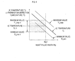
- FIGS. 4A to 4C show waveforms of the battery-voltage detection signals outputted from the voltage detection IC 6 to the microcomputer 5.
- the battery-voltage detection signal includes a reset pulse P having a predetermined pulse width (reset pulse width Wp) and cell voltage signals outputted in sequence at a predetermined timing after output of the reset pulse P.
- a voltage of high level (for example, DC 3.3 V) is outputted from the voltage detection IC 6 to the microcomputer 5.
- the reset pulse P is a binary signal in which the level of the voltage becomes a low level in the reset pulse width Wp.
- the cell voltage signal is not a binary signal, but an analog voltage signal corresponding to a voltage of each of the cell groups.
- one-half of the measured voltage value of each of the cell groups is outputted as the cell voltage signal.
- the cell voltage signal is outputted in the following order: a first cell voltage V1 which is a voltage of the cell group composed of the cells 21 and 22; a second cell voltage V2 which is a voltage of the cell group composed of the cells 23 and 24; a third cell voltage V3 which is a voltage of the cell group composed of the cells 25 and 26; a fourth cell voltage V4 which is a voltage of the cell group composed of the cells 27 and 28; and a fifth cell voltage V5 which is a voltage of the cell group composed of the cells 29 and 30.
- the voltage detection IC 6 includes an oscillator 18 which generates a clock signal CK.
- a timing of outputting the battery-voltage detection signal i.e., a timing of a rise in the reset pulse P, a timing of starting output of the cell voltage signal, and so on is in synchronization with the clock signal CK.
- the reset pulse width Wp is set to be 158 clocks (i.e., 158 cycles of the clock signal CK). Moreover, not only a time interval from when the reset pulse P is outputted to when output of the cell voltage signal is started, but also an output interval of each of the cell voltages V1 to V5 which constitute the cell voltage signal, is defined by a number of the clock signals CK (a number of clocks). Therefore, if a frequency of the clock signal CK (clock frequency) is constant, the reset pulse width Wp, a timing of output of the cell voltage signal, and the output interval of each of the cell voltages V1 to V5 are always constant.
- the oscillator 18 in the present embodiment is configured as a so-called CR oscillator using a resistor and a capacitor, the oscillator 18 is highly dependent on temperature and therefore, the clock frequency changes depending on a temperature inside of the battery pack 1 (specifically, a temperature of the voltage detection IC 6, and more specifically, a temperature of the oscillator 18).
- the clock frequency is 10 KHz at a temperature of 20°C; however, the clock frequency becomes higher as the temperature exceeds 20°C. On the other hand, the clock frequency becomes lower as the temperature decreases below 20°C.
- the reset pulse width Wp is about 15.8 msec as shown in FIG. 4B .
- the reset pulse width Wp becomes shorter such as about 13 msec, as shown in FIG. 4A , due to an increase of the clock frequency.
- the temperature is low, for example, minus 30°C, the reset pulse width Wp becomes longer such as about 19 msec, as shown in FIG. 4C , due to a decrease of the clock frequency.
- FIG. 5A shows one example of a reset pulse width VS temperature characteristic indicating a relationship between the reset pulse width Wp and the temperature. As shown in FIG. 5A , the reset pulse width Wp decreases substantially in a linear manner as the temperature increases.
- the microcomputer 5 detects the temperature, as will be described later, based on the reset pulse width Wp of the reset pulse P from the voltage detection IC 6. It can be said that the temperature detected based on the reset pulse width Wp directly represents the temperature of the oscillator 18. Moreover, it can be said that the temperature detected based on the reset pulse width Wp represents, in a broader sense, the temperature of the voltage detection IC 6 and represents, in a yet broader sense, the temperature inside of the battery pack 1. In the following description, therefore, the temperature detected by the microcomputer 5 based on the reset pulse width Wp is referred to as "IC temperature Tc".
- the thermistor 3 is provided to detect specifically a temperature of the battery 2 among the temperatures inside of the battery pack 1.
- the thermistor 3 is provided inside the battery 2 (specifically, on a side surface of the cell 27) as described above.
- One end of the thermistor 3 is connected to a ground in the battery control circuit 4.
- the other end of the thermistor 3 is connected to the microcomputer 5 in the battery control circuit 4.
- the power-supply voltage Vdd is applied to the other end of the thermistor 3 via a resistor R1.
- the power-supply voltage Vdd is divided by the thermistor 3 and the resistor R1, and the divided value is inputted to the microcomputer 5 as "thermistor-detection voltage Vt".
- the thermistor 3 is a known temperature detection element whose resistance value changes depending on temperatures.
- the thermistor 3 is an NTC (Negative Temperature Coefficient) thermistor whose resistance value decreases substantially in a linear manner as the temperature increases.
- the thermistor 3 may be a PTC (Positive Temperature Coefficient) thermistor whose resistance value increases substantially in a linear manner as the temperature increases.
- FIG. 5B shows one example of a thermistor-detection voltage VS temperature characteristic indicating a relationship between the thermistor-detection voltage Vt from the thermistor 3 and the temperature. Based on the thermistor-detection voltage VS temperature characteristic, the microcomputer 5 calculates a temperature corresponding to the thermistor-detection voltage Vt, as "thermistor-detection temperature Tt".
- the thermistor-detection temperature Tt detected by the thermistor 3 directly represents the temperature of the battery 2. Moreover, it can be said that, in a broader sense, the thermistor-detection temperature Tt detected by the thermistor 3 indirectly represents a temperature of the control board 10 in a vicinity of the battery 2, and in a yet broader sense, represents the temperature inside of the battery pack 1.
- the switch operation detection circuit 8 detects that the trigger switch (not shown) provided in the main body 40 is operated by the user.
- the switch operation detection circuit 8 includes a transistor Q1 and resistors R2, R3, and R4.
- the transistor Q1 is an NPN bipolar transistor. A base of the transistor Q1 is connected to the signal terminal 13A through the resistor R2 while being connected to the ground of the battery pack 1 through the resistor R3. An emitter of the transistor Q1 is connected to the ground.
- the ground of the battery pack 1 is connected to the negative power supply line L1B. Therefore, when the battery pack 1 is attached to the main body 40, the ground of the battery pack 1 and the ground of the main body 40 have a same electric potential to each other, and each of these grounds has a same electric potential as a negative electrode of the battery 2.
- a collector of the transistor Q1 is connected to the microcomputer 5 and also connected, through the resistor R4, to an output path of the power supply voltage Vdd from the control power supply circuit 16.
- the control power supply circuit 16 receives the battery voltage (DC 18 V) from the battery 2 or a power supply voltage Vee (for example, DC 5 V) from the battery charger 50, to generate a constant power supply voltage Vdd (for example, DC 3.3 V). Then, the control power supply circuit 16 performs power supply to various electronic circuits, including the battery control circuit 4, in the battery pack 1.
- the control power supply circuit 16 is constituted by, for example, a switching power circuit and the like.
- the power supply from the battery 2 to the control power supply circuit 16 is performed through the shutdown switch 17 and a back-flow inhibiting diode D3.
- the power supply from the battery charger 50 to the control power supply circuit 16 is performed through the signal terminal 13C and a back-flow inhibiting diode D4.
- the control power supply circuit 16 When the battery charger 50 is not connected to the control power supply circuit 16, in other words when the power-supply voltage Vee is not supplied to the control power supply circuit 16 from the battery charger 50 via the signal terminal 13C, the control power supply circuit 16 lowers the voltage of the battery 2 to generate the power-supply voltage Vdd.
- the control power supply circuit 16 lowers the supplied power-supply voltage Vee to generate the power-supply voltage Vdd.
- the shutdown switch 17 is normally in an ON state.
- the shutdown switch 17 is turned off in an overdischarge state where the voltage of the battery 2 decreases below a predetermined voltage level.
- the microcomputer 5 monitors the voltages V1 to V5 of the cell groups constituting the battery 2 or an overall voltage of the battery 2, based on the battery-voltage detection signal from the voltage detection IC 6. Then, in a case where at least one of the voltages V1 to V5 becomes equal to or less than a predetermined cell-voltage threshold value or in a case where the overall voltage of the battery 2 becomes equal to or less than a predetermined battery-voltage threshold value, the battery control circuit 4 determines that the battery 2 is in the overdischarge state, and turns off the shutdown switch 17.
- the shutdown switch 17 When the shutdown switch 17 is turned off, an electric power from the battery 2 is not supplied to the control power supply circuit 16. Consequently, output of the power-supply voltage Vdd from the control power supply circuit 16 is suspended, and thus, operation of the battery control circuit 4 is suspended.
- the shutdown switch 17, which has been turned off, is turned on when the battery pack 1 is connected to the battery charger 50, as will be explained later.
- the transistor Q2 is an N-channel MOSFET. A drain of the transistor Q2 is connected to the signal terminal 13A. Furthermore, a source of the transistor Q2 is connected to the ground. A gate of the transistor Q2 is connected to the microcomputer 5.
- the transistor Q2 is turned on/off by an output signal (a discharge control signal, which will be explained later) from the microcomputer 5.
- an output signal (a discharge control signal, which will be explained later) from the microcomputer 5.
- the main switch 36 ON
- the transistor Q2 is in an OFF state
- a high level signal corresponding to the power supply voltage Vcc in the main body 40 is inputted from the signal terminal 33 of the main body 40 to the signal terminal 13A of the battery pack 1.
- the transistor Q1 in the switch operation detection circuit 8 is brought into an ON state, and an input signal from the switch operation detection circuit 8 to the microcomputer 5 becomes low level.
- the trigger switch is not operated (the main switch 36: OFF)
- the electric potential of the signal terminal 33 of the main body 40 is low level (a ground potential); then, the transistor Q1 in the switch operation detection circuit 8 is brought into an OFF state, and the input signal from the switch operation detection circuit 8 to the microcomputer 5 becomes high level.
- the battery charger detection circuit 9 is configured in a same manner as the switch operation detection circuit 8. Specifically, the battery charger detection circuit 9 is configured such that when the battery pack 1 is attached to the battery charger 50 and a high level signal (in the present embodiment, the power-supply voltage Vee of DC 5 V) is inputted from the battery charger 50 to the signal terminal 13C, the battery charger detection circuit 9 inputs, to the microcomputer 5, a detection signal indicating that the battery pack 1 is attached to the battery charger 50.
- a high level signal in the present embodiment, the power-supply voltage Vee of DC 5 V
- the battery charger detection circuit 9 inputs a high level signal corresponding to the power supply voltage Vdd to the microcomputer 5 through a pull-up resistor (not shown).
- a transistor (not shown) connected to a signal path to the microcomputer 5 is brought into an ON state, and this signal path is connected to the ground to make an output to the microcomputer 5 low level.
- the microcomputer 5 can detect that the trigger switch has been operated in the main body 40 to which the battery pack 1 is attached, based on the input signal from the switch operation detection circuit 8. Also, the microcomputer 5 can detect that the battery pack 1 has been attached to the battery charger 50 based on the input signal from the battery charger detection circuit 9.
- An anode of the diode D2 is connected to the microcomputer 5.
- a cathode of the diode D2 is connected to the signal terminal 13D.
- the power-supply voltage Vdd is applied to the anode of the diode D2 through a pull-up resistor R5.
- the cathode of the diode D2 is, as shown in FIG. 3 , connected to the ground in the battery charger 50 through the signal terminal 13D and the signal terminal 53C.
- a forward voltage (hereinafter, referred to as "diode voltage") Vf of the diode D2 is inputted to the microcomputer 5.
- the ground of the battery pack 1 and the ground of the battery charger 50 are electrically connected to each other through the negative electrode terminal 12 and a negative electrode terminal 52.
- the battery pack 1 and the battery charger 50 are also connected electrically to each other, as shown in FIG. 3 .
- the battery charger 50 includes a positive electrode terminal 51, the negative electrode terminal 52, and the signal terminals 53A, 53B, and 53C.
- the positive electrode terminal 51 and the negative electrode terminal 52 are provided for connecting, respectively, to the positive electrode terminal 11 and the negative electrode terminal 12 of the battery pack 1.
- the signal terminals 53A, 53B, and 53C are provided for connecting, respectively, to the signal terminals 13B, 13C, and 13D of the battery pack 1.
- the battery charger 50 includes a rectifier circuit 55, a charging switching power supply circuit 56, a main control unit (MCU) 57, and a controlling switching power supply circuit 58.
- the rectifier circuit 55 rectifies alternate current (AC) power supplied from an AC power source such as a commercial power source. Such a rectified output from the rectifier circuit 55 is outputted to the charging switching power supply circuit 56 and the controlling switching power supply circuit 58.
- AC alternate current
- the charging switching power supply circuit 56 is a switching circuit that performs charging to the battery 2 based on the output from the rectifier circuit 55; the charging switching power supply circuit 56 is drive-controlled by the MCU 57.
- the MCU 57 is constituted by a microcomputer, in the same manner as in the microcomputer 5 in the battery pack 1.
- the MCU 57 acquires a control signal (analog voltage signal) from the microcomputer 5 in the battery control circuit 4 through the signal terminals 13A and 53A and controls patterns of charging to the battery 2 (charge current, charge voltage, etc.) by drive-controlling the charging switching power supply circuit 56 in accordance with the control signal.
- the controlling switching power supply circuit 58 generates the power supply voltage Vee (DC 5 V in the present embodiment, as already described above) for operating an internal circuit inside the battery charger 50, such as the MCU 57 and the like.
- the ground of the battery charger 50 is connected to the negative electrode terminal 2B of the battery 2, through the negative electrode terminal 52 and the negative electrode terminal 12.
- a charge voltage generated in the charging switching power supply circuit 56 is applied to the positive electrode terminal 2A of the battery 2, through the positive electrode terminal 51 and the positive electrode terminal 11.
- the power supply voltage Vee generated in the controlling switching power supply circuit 58 is applied.
- a high level signal corresponding the power supply voltage Vee is inputted to the battery charger detection circuit 9 through the signal terminals 53B and 13C. Then, a signal level of a detection signal inputted from the battery charger detection circuit 9 to the microcomputer 5 changes from high level to low level.
- the microcomputer 5 monitors detection signals from the switch operation detection circuit 8 and the battery charger detection circuit 9.
- the microcomputer 5 makes the discharge control signal high level to turn on the transistor Q2 and allows discharge from the battery 2 to the drive motor M1.
- the transistor Q2 when the transistor Q2 is brought into an ON state, the transistor Q4 in the input/output circuit 35 in the main body 40 is brought into an OFF state and the transistor Q3 provided on the current path to the drive motor M1 is brought into an ON state; consequently, a current flows through the drive motor M1 to rotate the drive motor M1.
- the microcomputer 5 When the microcomputer 5 makes the discharge control signal high level as such and allows the discharge from the battery 2 to the drive motor M1 (i.e., during the discharge from the battery 2), the microcomputer 5 executes various protection processes that monitor the battery 2 so as to protect the battery 2 from overdischarge and the like.
- a discharge current limitation process As the aforementioned various protection processes, a discharge current limitation process, an overdischarge limitation process, and a battery temperature limitation process are performed. These three processes limit the discharge from the battery 2 to the drive motor M1 based on detection results by the voltage detection IC 6, the current measurement circuit 7, and the thermistor 3.
- the discharge current limitation process performs various limitations which include, for example, following limitations: it is periodically and cumulatively detected whether or not overcurrent is flowing based on the discharge current detected in the current measurement circuit 7 during the discharge, and if the overcurrent is flowing, it is periodically and cumulatively detected what level the overcurrent is, etc.; then, depending on results of the detection, the discharge is allowed, suspended, or others.
- the overdischarge limitation process suspends the discharge from the battery 2 to the drive motor M1 in the following manner: based on the battery voltage detected in the voltage detection IC 6 during the discharge, if at least one cell group of the cell groups has a voltage equal to or less than a preset cell-voltage threshold value or if a voltage of the battery 2 is equal to or less than a preset battery-voltage threshold value, it is determined that the battery 2 is in the overdischarge state; then, the discharge control signal is made low level, thereby suspending the discharge from the battery 2 to the drive motor M1.
- an above-described process for turning off the shutdown switch 17 is also performed if it is determined that the battery 2 is in the overdischarge state.
- an output state (a timing of level change, etc.) of the battery-voltage detection signal outputted from the voltage detection IC 6 changes depending on a temperature. Therefore, every time the battery-voltage detection signal is inputted to the microcomputer 5 from the voltage detection IC 6, the microcomputer 5 measures the reset pulse width Wp of the reset pulse P, corrects the battery-voltage detection signal based on results of the measurement, and obtain each of the cell voltages V1-V5 of the respective cell groups.
- the discharge control signal is made low level, thereby suspending the discharge from the battery 2 to the drive motor M1.
- the microcomputer 5 Since the microcomputer 5 continues to output the discharge control signal (high level) unless it is determined that an abnormality such as overcurrent is occurred in the above-described limitation processes, the microcomputer 5 cannot detect an OFF state of the main switch 36 (in other words, a suspension of operation of the trigger switch) through the switch operation detection circuit 8.
- the microcomputer 5 while the discharge control signal is high level, the microcomputer 5 periodically makes the discharge control signal low level for a very short period of time, to monitor the detection signal from the switch operation detection circuit 8 at this low level of the discharge control signal. Thereby, the microcomputer 5 determines an operation state of the main switch 36.
- the microcomputer 5 when the detection signal from the battery charger detection circuit 9 becomes low level as a result of attachment of the battery pack 1 to the battery charger 50, the microcomputer 5 outputs various information indicating a status (battery voltage, battery capacity, ant the like) of the battery 2 to the MCU 57 of the battery charger 50 through the signal terminals 13B and 53A. Thereafter, when charge from the battery charger 50 to the battery 2 is started, the microcomputer 5 executes a charge control process for battery protection.
- the power-supply voltage Vdd is not supplied to the microcomputer 5, thereby suspending an operation of the microcomputer 5.
- the battery charger 50 is connected to the battery pack 1
- the power-supply voltage Vee in the battery charger 50 is supplied to the battery pack 1.
- the power-supply voltage Vdd is generated to make the microcomputer 5 start operating again.
- the microcomputer 5 starts operating again by the supply of the power-supply voltage Vdd, the microcomputer 5 turns on the shutdown switch 17 again.
- the microcomputer 5 realizes two functions, which will be explained below, based on the diode voltage Vf detected by the diode D2.
- One of the two functions is to detect an output abnormality of the control power supply circuit 16.
- the control power supply circuit 16 lowers the power-supply voltage Vee (DC 5 V) from the battery charger 50 to the power-supply voltage Vdd (DC 3.3 V) when the battery pack 1 is connected to the battery charger 50.
- the power-supply voltage Vdd which is 3.3 V in a normal state, may become 5 V in an abnormal state.
- the microcomputer 5 of the present embodiment recognizes each of the cell voltages V1 to V5 as follows: an "AD value” (a value which has been AD converted) of the cell voltage, which is inputted from the voltage detection IC 6, of each of the cell voltages V1 to V5 is divided by an "AD value" of the power-supply voltage Vdd; and a result of the division is recognized as a cell voltage of each of the cell voltages V1 to V5.
- an AD conversion is performed by, for example, an 8-bit (0-255) AD converter.
- the microcomputer 5 erroneously recognizes the cell voltage as having a value lower than an actual value. Since it is not desirable that the cell voltage becomes overvoltage, it is vital to detect the aforementioned malfunction in the control power supply circuit 16. In order to detect the malfunction, the diode D2 is used.
- the microcomputer 5 When the microcomputer 5 recognizes the diode voltage Vf as the numerical value of "47", the microcomputer 5 determines that the power-supply voltage Vdd has a normal value without any malfunctions, etc.
- the microcomputer 5 When the microcomputer 5 recognizes the diode voltage Vf as the numerical value of "31", the microcomputer 5 determines that the power-supply voltage Vdd has an abnormal value due to a malfunction, etc. in the control power supply circuit 16.
- the diode voltage Vf of the diode D2 is normally 0.6 V.
- the diode voltage Vf may vary due to various factors such as individual differences of elements or ambient temperature, etc. If, for example, there is a possibility in which the diode voltage Vf varies in a range of 0.5 V to 0.7 V, the numerical value recognized by the microcomputer 5 would also varies, as illustrated in FIG. 6 .
- the numerical value of the diode voltage Vf recognized by the microcomputer 5 varies in a range of "39" to "54".
- the power-supply voltage Vdd is abnormal (for example, 5 V)
- the numerical value of the diode voltage Vf recognized by the microcomputer 5 varies in a range of "26" to "36".
- the microcomputer 5 determines that the power-supply voltage Vdd is normal. On the other hand, if the numerical value recognized as the diode voltage Vf deviates from the range of "39" to "54", the microcomputer 5 determines that the power-supply voltage Vdd is abnormal and that a malfunction occurs.
- the numerical value recognition of the diode voltage Vf by the microcomputer 5 and a determination of whether or not a malfunction exists based on such a recognized numerical value are performed, for example, when the battery pack 1 is connected to the battery charger 50 (i.e., when this connection is recognized by the microcomputer 5).
- the other of the two functions realized by the microcomputer 5 by using the diode D2 is to correct an analog control signal which the microcomputer 5 outputs to the battery charger 50 during charge.
- the microcomputer 5 of the battery pack 1 and the microcomputer (MCU) 57 of the battery charger 50 are connected to each other via the respective signal terminals 13B and 53A. While the battery charger 50 is connected to the battery pack 1, the microcomputer 5 outputs a control signal for controlling the battery charger 50, to the MCU 57 via the signal terminals 13B and 53A.
- a ground potential of the microcomputer 5 becomes higher than a ground potential of the MCU 57 due to various factors, for example, a contact resistance between the negative electrode terminals 12 and 52.
- the MCU 57 may recognize that a value of the control signal outputted from the microcomputer 5 is different from the voltage value outputted from the microcomputer 5.
- the microcomputer 5 outputs, for example, a voltage of 3 V as the control signal, the MCU 57 may recognize that the control signal has 3.1 V. Therefore, the microcomputer 5 cannot correctly control the battery charger 50.
- the microcomputer 5 detects the IC temperature Tc based on the battery-voltage detection signal from the voltage detection IC 6 (specifically, based on the reset pulse width Wp). In addition, the microcomputer 5 executes a thermistor abnormality determination process. The thermistor abnormality determination process is to determine whether or not a malfunction exists in the thermistor 3 based on the detected IC temperature Tc.
- the thermistor 3 is provided in the battery 2, and the voltage detection IC 6 is disposed on the control board 10 located at an upper part of the battery 2. Therefore, it is expected that the thermistor-detection temperature Tt detected by the thermistor 3 and the IC temperature Tc detected based on the reset pulse width Wp from the voltage detection IC 6 are not completely the same as each other, but are not greatly different from each other and are relatively closer to each other.
- the thermistor-detection temperature Tt is greatly different from the IC temperature Tt, it is considered that the thermistor-detection temperature Tt is abnormal, in other words, the thermistor 3 is in an abnormal state.
- the microcomputer 5 determines whether or not the thermistor-detection temperature Tt is within a normal range (and therefore, whether or not the thermistor 3 is normal) based on the IC temperature Tc; if the thermistor 3 is abnormal, charge and/or discharge are limited or suspended.
- an abnormality in the thermistor 3 does not only mean an abnormality of the thermistor 3 itself.
- disconnection or short circuit of a wire connecting the thermistor 3 with the control board 10 is also included in the abnormality in the thermistor 3.
- an abnormality in which a normal detection signal cannot be obtained due to adherence of foreign substances to a wire from the thermistor 3 to the microcomputer 5, and so on is included in the abnormality in the thermistor 3.
- the abnormality in the thermistor 3 means any abnormalities which causes the correct thermistor-detection voltage corresponding to a temperature not to be inputted from the thermistor 3.
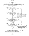
- FIGS. 7A and 7B the thermistor abnormality determination process executed by the microcomputer 5 is shown.
- the input triggers the microcomputer 5 to execute the thermistor abnormality determination process.
- the microcomputer 5 When the thermistor abnormality determination process is stared, the microcomputer 5 first measures the reset pulse width Wp of the reset pulse P (S110). Based on the reset pulse width VS temperature characteristic illustrated in FIG. 5A , the IC temperature Tc corresponding to the measured reset pulse width Wp is calculated (S120).
- the thermistor-detection voltage Vt is obtained from the thermistor 3 (S130). Then, based on the thermistor voltage VS temperature characteristic illustrated in FIG. 5B , the thermistor-detection temperature Tt corresponding to the obtained thermistor-detection voltage Vt is calculated (S140).
- a maximum value Tt_max and a minimum value Tt_min in a temperature range which is expected to be the thermistor-detection temperature Tt are calculated (estimated) respectively based on the IC temperature Tc (S150).
- a map is pre-set in which respective characteristics of the maximum value Tt_max and the minimum value Tt_min of the expected thermistor-detection temperature Tt are mapped to the characteristic of the IC temperature Tc. For example, if the reset pulse width Wp is "Wp1" and the IC temperature Tc corresponding to Wp1 is "Tc1", the maximum value Tt_max and the minimum value Tt_min corresponding to an IC temperature Tc1 are calculated, respectively, as Tt_max1 and Tt_min1, based on the map.
- the microcomputer 5 calculates the maximum value Tt_max and the minimum value Tt_min corresponding to the IC temperature Tc, by using the map.
- the maximum value Tt_max and the minimum value Tt_min may be calculated by other ways (for example, by a numerical operation, etc.).
- the thermistor-detection temperature Tt is less than the maximum value Tt_max (S160). In this case, if the thermistor-detection temperature Tt is less than the maximum value Tt_max (S160: YES), it is subsequently determined whether or not the thermistor-detection temperature Tt is greater than the minimum value Tt_min (S170). If the thermistor-detection temperature Tt is greater than the minimum value Tt_min (S170: YES), the thermistor 3 is determined not to be abnormal (i.e., to be normal)(S180) and the thermistor abnormality determination process is terminated.
- the thermistor-detection temperature Tt is equal to or greater than the maximum value Tt_max (S160: NO) or if the thermistor-detection temperature Tt is equal to or less than the minimum value Tt_min (S170: NO), it is determined that some abnormality exists in the thermistor 3 (S190).
- a command to suspend (or limit) the charge is outputted (S220).
- the suspension (or limitation) of the charge is achieved by transmitting a command signal to suspend the charge or reduce the charge current, to the battery charger 50 through the signal terminal 13B.
- the microcomputer 5 detects the IC temperature Tc by using a temperature dependence of the battery-voltage detection signal outputted from the voltage detection IC 6 (specifically, a temperature dependence of the reset pulse width Wp). Then, the microcomputer 5 detects whether or not an abnormality exists in the thermistor 3 based on the detected IC temperature Tc. Therefore, in the present embodiment, it is possible to provide the battery pack 1 having a higher liability and capable of detecting whether or not an abnormality exists in the thermistor 3.
- the IC temperature Tc is detected, not by using an independent temperature-detection element like a thermistor, but by using the voltage detection IC 6 originally provided in the battery pack 1. That is to say, it is not necessary to separately provide a temperature-detection element in order to detect the IC temperature Tc (and therefore, to detect whether or not an abnormality exists in the thermistor 3), and this detection can be achieved by effectively utilizing an already existing configuration.
- the detection of the IC temperature Tc is achieved by a simple way in which the detection is performed based on the reset pulse width Wp from the voltage detection IC 6.
- the IC temperature Tc is obtained by the calculation based on the reset pulse width Wp, such an obtained temperature may be less accurate than the thermistor-detection temperature Tt obtained by the thermistor 3.
- the microcomputer 5 cannot detect the abnormal state based on the detection signal (the thermistor-detection voltage Vt) from the thermistor 3.
- the microcomputer 5 can determine whether or not the voltage detection IC 6 is normal based on a state of the battery-voltage detection signal inputted to the microcomputer 5 (for example, based on whether or not the reset pulse is periodically inputted).
- the voltage detection IC 6 is normal; therefore, the IC temperature Tc based on the reset pulse width Wp is considered to be a reliable value. Accordingly, as long as the voltage detection IC 6 operates normally, whether or not an abnormality exists in the thermistor 3 is reliably determined based on the IC temperature Tc.
- the battery pack 1 corresponds to an example of a battery pack of the present invention and the battery control circuit 4 corresponds to an example of a temperature detection device of the present invention.
- the voltage detection IC 6 corresponds to an example of a signal output circuit of the present invention
- the microcomputer 5 corresponds to an example of an output signal-based temperature detection unit of the present invention, an example of a temperature detection signal-based temperature detection unit of the present invention, an example of a threshold value-based abnormality determination unit of the present invention, and an example of a protection command output unit of the present invention
- the oscillator 18 corresponds to an example of a clock generation circuit of the present invention
- the thermistor 3 corresponds to an example of a temperature detection element of the present invention
- each of a difference between the maximum value Tt_max and the IC temperature Tc and a difference between the minimum value Tt_min and the IC temperature Tc corresponds to an example of a detected-temperature difference threshold value of the present invention.
- the thermistor-detection temperature Tt is equal to or greater than the maximum value Tt_max (S160: NO) or if the thermistor-detection temperature Tt is equal to or less than the minimum value Tt_min (S170: NO).
- the microcomputer 5 performs a various protection operations based on the detected temperature by the thermistor 3, and the IC temperature Tc is used only to determine whether or not an abnormality occurs in the thermistor 3; however, such various protection operations may be performed based on the IC temperature Tc.
- various control processes may be performed by using, as needed, respective temperatures of two positions, i.e., the IC temperature Tc and the thermistor-detection temperature Tt.
- a number of positions are not limited to the aforementioned two locations but may be any number of positions inside the battery pack 1.
- it may be configured such that, in a case where the IC temperature Tc and the thermistor-detection temperature Tt are compared with each other and a difference between the IC temperature Tc and the thermistor-detection temperature Tt is equal to or greater than a predetermined detected-temperature difference threshold value, it is determined that at least one of the aforementioned two temperatures is abnormal (i.e., at least one of the voltage detection IC 6 and the thermistor 3 is abnormal).
- a temperature inside the battery pack 1 may be monitored based on the IC temperature Tc, so as to perform the various protection operations based on the IC temperature Tc.
- the thermistor-detection temperature Tt and the IC temperature Tc can be also used as follows.
- a temperature abnormality determination function may be provided, and in this function, when at least one of the thermistor-detection temperature Tt and the IC temperature Tc becomes equal to or greater than a predetermined temperature upper-limit value or becomes equal to or less than a predetermined temperature lower-limit value which is lower than the temperature upper-limit value, an abnormality is determined to occur in the battery pack 1.
- a temperature-change rate abnormality determination function may be provided.
- a change rate ⁇ Tt of the thermistor-detection temperature Tt and a change rate ⁇ Tc of the IC temperature Tc are calculated, and when at least one of the two change rates ⁇ Tt and ⁇ Tc becomes equal to or greater than a predetermined change rate upper-limit value, an abnormality is determined to occur in the battery pack 1.
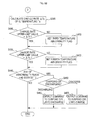
- FIGS. 9A and 9B show one example of a battery temperature abnormality determination process executed by a microcomputer in a battery pack provided with the temperature abnormality determination function and the temperature-change rate abnormality determination function.
- the microcomputer in the battery pack can periodically execute the battery temperature abnormality determination process, for example, in parallel to the thermistor abnormality determination process in FIGS. 7A and 7B .
- the thermistor-detection temperature Tt and the IC temperature Tc are obtained (S310).
- the thermistor-detection temperature Tt and the IC temperature Tc can be obtained, for example, by calculation in the same procedures as those in S110 to S140 in the thermistor abnormality determination process in FIGS. 7A and 7B .
- the microcomputer 5 determines whether or not the obtained thermistor-detection temperature Tt is less than a predetermined temperature upper-limit value (S320), and then whether or not the obtained thermistor-detection temperature Tt is greater than a predetermined temperature lower-limit value (S330). In this case, if the thermistor-detection temperature Tt is equal to or greater than the temperature upper-limit value (S320: NO), or equal to or less than the temperature lower-limit value (S330: NO), a first temperature abnormality flag is set (S340).
- the microcomputer 5 determines whether or not the obtained IC temperature Tc is below the predetermined temperature upper-limit value (S350), and then, whether or not the obtained IC temperature Tc is greater than the predetermined temperature lower-limit value (S360).
- a second temperature abnormality flag is set (S370).
- the microcomputer 5 calculates a change rate ⁇ Tt of the thermistor-detection temperature Tt (S380) and a change rate ⁇ Tc of the IC temperature Tc (S390). These change rates ⁇ Tt and ⁇ Tc can be calculated, for example, by calculating a rate of change (difference) from the temperatures Tt and Tc obtained in S310 during previous execution of the battery temperature abnormality determination process, to the temperatures Tt and Tc obtained in the battery temperature abnormality determination process this time.
- the microcomputer 5 determines whether or not the change rate ⁇ Tt of the thermistor-detection temperature Tt is less than a predetermined change rate upper-limit value (S400). If the change rate ⁇ Tt is equal to or greater than the change rate upper-limit value (S400: NO), the microcomputer 5 sets a third temperature abnormality flag (S410).
- the microcomputer 5 determines whether or not the change rate ⁇ Tc of the IC temperature Tc is less than the predetermined change rate upper-limit value (S420).
- the microcomputer 5 sets a fourth temperature abnormality flag (S430).
- the microcomputer 5 determines whether or not at least one of the aforementioned four abnormality flags has been set (S440). If any of the four abnormality flags has not been set (S440: NO), the microcomputer 5 terminates the battery temperature abnormality determination process. On the other hand, if any of the four abnormality flags has been set, the microcomputer 5 proceeds to the subsequent S450 onwards, and to suspend or limit corresponding operations of charge or discharge depending on whether the charge to the battery 2 or the discharge from the battery 2 is performed.
- the processes in S450 onwards are the same as those in S200 onwards in the thermistor abnormality determination process in FIGS. 7A and 7B .
- the microcomputer 5 executes the battery temperature abnormality determination process in FIGS. 9A and 9B in the above-explained manner.
- the following abnormality detection becomes possible: for example, if the temperature of the battery 2 exceeds or falls below a rated temperature range, an abnormality is determined to exist by detecting such an excess or such a fall; also, an abnormality is determined to exist by detecting overheat in other circuits (e.g., the battery control circuit 4, etc.) than the battery 2.
- the abnormality is determined to exist, if the charge to the battery 2 or the discharge from the battery 2 is performed, the discharge or charge may be suspended or limited.
- the microcomputer 5 corresponds to an example of a detected temperature-based abnormality determination unit of the present invention, an example of a change rate-based abnormality determination unit of the present invention, and an example of a protection command output unit of the present invention.
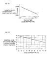
- the diode voltage (forward voltage) Vf of the diode D2 has a temperature dependence, as in the case of the reset pulse width Wp. As illustrated in FIG. 10A , the diode voltage Vf changes substantially in a linearly manner in accordance with the temperature (diode temperature) of the diode D2 itself. Specifically, as the diode temperature becomes higher, the diode voltage Vf becomes smaller. Accordingly, the numerical value (AD value) of the diode voltage Vf, which is to be recognized by the microcomputer 5, changes in accordance with the diode temperature, as shown in FIG. 10B .
- the diode temperature is estimated from the diode voltage Vf; based on the estimated diode temperature, it is possible to detect whether or not an abnormality exists in the thermistor.
- the aforementioned abnormality detection of whether or not an abnormality exists in the output voltage (the power-supply voltage Vdd) of the control power supply circuit 16 based on the diode voltage Vf, is firstly executed.
- the diode temperature is estimated based on the diode voltage Vf at a time of this determination.
- the estimated diode temperature is compared with the thermistor-detection temperature Tt. If a difference between the estimated diode temperature and the thermistor-detection temperature Tt is within a predetermined range, it can be determined that the thermistor 3 is normal. On the other hand, the difference goes beyond the predetermined range, it can be determined that the thermistor 3 is abnormal.
- the abnormality detection of the thermistor 3 based on the diode voltage Vf can be performed by utilizing circuits and the like originally provided in the battery pack 1, in other words, the originally provided diode D2, as in the case of the abnormality detection based on the reset pulse width Wp.
- the battery 2 is the lithium-ion rechargeable battery.
- the battery 2 may be other rechargeable batteries for example, a nickel -hydride rechargeable battery, a nickel-cadmium rechargeable battery or the like.
- the present invention may be applied to any electric power tool other than a driver drill.
- a brushed DC motor is employed as the drive motor M1.
- a brushless DC motor or an AC motor may be employed as the drive motor M1.
Landscapes
- Engineering & Computer Science (AREA)
- Manufacturing & Machinery (AREA)
- Chemical & Material Sciences (AREA)
- Chemical Kinetics & Catalysis (AREA)
- Electrochemistry (AREA)
- General Chemical & Material Sciences (AREA)
- Secondary Cells (AREA)
- Battery Mounting, Suspending (AREA)
- Charge And Discharge Circuits For Batteries Or The Like (AREA)
Applications Claiming Priority (1)
| Application Number | Priority Date | Filing Date | Title |
|---|---|---|---|
| JP2011237270A JP5951959B2 (ja) | 2011-10-28 | 2011-10-28 | 温度検出装置及びバッテリパック |
Publications (3)
| Publication Number | Publication Date |
|---|---|
| EP2587584A2 true EP2587584A2 (de) | 2013-05-01 |
| EP2587584A3 EP2587584A3 (de) | 2015-05-06 |
| EP2587584B1 EP2587584B1 (de) | 2017-01-18 |
Family
ID=47073357
Family Applications (1)
| Application Number | Title | Priority Date | Filing Date |
|---|---|---|---|
| EP12190247.2A Not-in-force EP2587584B1 (de) | 2011-10-28 | 2012-10-26 | Temperaturdetektionsvorrichtung und Batteriesatz |
Country Status (5)
| Country | Link |
|---|---|
| US (1) | US20130108904A1 (de) |
| EP (1) | EP2587584B1 (de) |
| JP (1) | JP5951959B2 (de) |
| CN (1) | CN103090983A (de) |
| RU (1) | RU2012145792A (de) |
Cited By (2)
| Publication number | Priority date | Publication date | Assignee | Title |
|---|---|---|---|---|
| EP3346574A1 (de) * | 2017-01-10 | 2018-07-11 | HTC Corporation | Tragbare elektronische vorrichtung, ladesystem, verbinder und ladeverwaltungsverfahren dafür |
| US10950912B2 (en) | 2017-06-14 | 2021-03-16 | Milwaukee Electric Tool Corporation | Arrangements for inhibiting intrusion into battery pack electrical components |
Families Citing this family (39)
| Publication number | Priority date | Publication date | Assignee | Title |
|---|---|---|---|---|
| JP4807443B2 (ja) * | 2009-07-08 | 2011-11-02 | トヨタ自動車株式会社 | 二次電池の温度推定装置 |
| JP5554622B2 (ja) * | 2010-04-21 | 2014-07-23 | 株式会社マキタ | 電動工具用装置 |
| CN105705370B (zh) * | 2013-08-06 | 2018-03-23 | 睿能创意公司 | 基于电能储存装置热简况调节电动车系统 |
| CN103427123B (zh) * | 2013-08-26 | 2015-08-19 | 青岛海信电子设备股份有限公司 | 一种最大化使用电池容量的方法及手持终端 |
| CN103594753B (zh) * | 2013-10-19 | 2015-12-09 | 深圳市朗科智能电气股份有限公司 | 一种锂离子动力电池多点温控保护方法及装置 |
| JP6227420B2 (ja) | 2014-01-09 | 2017-11-08 | 株式会社マキタ | 電動工具用電池パック |
| DE102014208865A1 (de) * | 2014-05-12 | 2015-11-12 | Robert Bosch Gmbh | Verfahren zum Ermitteln der Temperatur einer Batterie |
| US9689753B2 (en) * | 2014-05-22 | 2017-06-27 | Roche Diabetes Care, Inc. | Handheld analyte meter with recharging control for improved analyte testing |
| JP6315417B2 (ja) | 2014-05-30 | 2018-04-25 | 日立工機株式会社 | 電動工具及び電池パック |
| JP2016022566A (ja) * | 2014-07-23 | 2016-02-08 | 株式会社マキタ | 電動機械器具 |
| JP6211493B2 (ja) | 2014-09-10 | 2017-10-11 | 矢崎総業株式会社 | 温度検出装置 |
| US20190149061A1 (en) * | 2015-07-14 | 2019-05-16 | Renun Mechanical & Electrical Co., Ltd | Power source device of electric tool |
| JP6767198B2 (ja) * | 2015-11-30 | 2020-10-14 | 株式会社マキタ | バッテリ装置及び充電装置 |
| JP2017133995A (ja) * | 2016-01-29 | 2017-08-03 | サンデンシステムエンジニアリング株式会社 | 温度測定装置 |
| JP6703265B2 (ja) * | 2016-06-27 | 2020-06-03 | 富士通株式会社 | ニューラルネットワーク装置及びニューラルネットワーク装置の制御方法 |
| US20180097376A1 (en) * | 2016-10-03 | 2018-04-05 | Hybrid Power Solutions Inc. | Battery pack and method of operation therefor |
| JP6760029B2 (ja) * | 2016-12-09 | 2020-09-23 | 株式会社デンソー | 温度センサ |
| JP6941787B2 (ja) * | 2017-01-23 | 2021-09-29 | パナソニックIpマネジメント株式会社 | 接触不良検出システム |
| GB2551081B (en) | 2017-08-18 | 2018-12-19 | O2Micro Inc | Fault detection for battery management systems |
| CN107678465A (zh) * | 2017-11-07 | 2018-02-09 | 厦门盈趣科技股份有限公司 | 温度控制系统及方法 |
| EP3490052B1 (de) * | 2017-11-24 | 2019-10-02 | Samsung SDI Co., Ltd. | Temperatursensorwärmekontakttestverfahren und -schaltung |
| CN109986967A (zh) * | 2017-12-30 | 2019-07-09 | 北京长城华冠汽车科技股份有限公司 | 一种电动汽车动力电池的均衡电路的故障诊断系统及其诊断方法 |
| CN108760083A (zh) * | 2018-07-03 | 2018-11-06 | 汉能移动能源控股集团有限公司 | 一种太阳能组件的工作温度检测方法及系统和异常预警及系统 |
| CN109000816B (zh) * | 2018-07-17 | 2020-05-22 | 环鸿电子(昆山)有限公司 | 电池温度感测电路 |
| CN109659635B (zh) * | 2019-01-21 | 2023-11-03 | 安徽安凯汽车股份有限公司 | 一种温度显示装置 |
| CN114883672B (zh) * | 2019-06-27 | 2025-04-29 | 奥动新能源汽车科技有限公司 | 电池包的安全处理装置、电力储能装置及其控制方法 |
| CN112490522A (zh) * | 2019-09-12 | 2021-03-12 | 北京小米移动软件有限公司 | 电池保护模组及方法、电池、移动终端 |
| CN111426724B (zh) * | 2019-10-23 | 2022-08-19 | 蜂巢能源科技有限公司 | 测试电极材料安全性能的方法 |
| DE102019216608A1 (de) * | 2019-10-29 | 2021-04-29 | Thyssenkrupp Ag | Batteriemodul mit Überwachung des thermischen Durchgehens von einzelnen Zellen |
| KR102321120B1 (ko) * | 2019-11-07 | 2021-11-03 | 송과모터스 주식회사 | 배터리팩의 보호 방법 및 이를 위한 장치 |
| CN110940924B (zh) * | 2019-12-17 | 2022-11-22 | 格力博(江苏)股份有限公司 | 一种电池包诊断方法以及电池包诊断装置 |
| DE102020104194A1 (de) * | 2020-02-18 | 2021-08-19 | Knorr-Bremse Systeme für Nutzfahrzeuge GmbH | Vorrichtung zur temperaturbestimmung |
| US12487132B2 (en) * | 2020-05-29 | 2025-12-02 | Samsung Sdi Co., Ltd. | Temperature-dependent resistor network for temperature anomaly monitoring in a battery system |
| JP7388318B2 (ja) * | 2020-09-02 | 2023-11-29 | トヨタ自動車株式会社 | 電源装置 |
| JP7239542B2 (ja) * | 2020-11-16 | 2023-03-14 | 矢崎総業株式会社 | 導電モジュール |
| JP7586753B2 (ja) * | 2021-03-30 | 2024-11-19 | 本田技研工業株式会社 | バッテリユニット |
| CA3157172A1 (en) | 2021-04-27 | 2022-10-27 | Techtronic Cordless Gp | Battery temperature based tool power reduction |
| CN115694364A (zh) * | 2021-07-27 | 2023-02-03 | 精工爱普生株式会社 | 电路装置以及振荡器 |
| US12466047B2 (en) | 2023-03-22 | 2025-11-11 | Milwaukee Electric Tool Corporation | Power tools including a plurality of temperature sensors |
Citations (2)
| Publication number | Priority date | Publication date | Assignee | Title |
|---|---|---|---|---|
| JP2000278878A (ja) | 1999-03-26 | 2000-10-06 | Makita Corp | 充電装置及び充電方式 |
| JP2001211559A (ja) | 2000-01-24 | 2001-08-03 | Makita Corp | 充電装置 |
Family Cites Families (17)
| Publication number | Priority date | Publication date | Assignee | Title |
|---|---|---|---|---|
| JPS5770417A (en) * | 1980-10-21 | 1982-04-30 | Citizen Watch Co Ltd | Temperature detecting device |
| FR2584344B1 (fr) * | 1985-07-03 | 1988-12-02 | Michelin & Cie | Circuit de codage de la valeur de deux grandeurs mesurees dans un pneumatique et dispositif de surveillance des pneumatiques utilisant un tel circuit |
| JPH02118425A (ja) * | 1988-06-17 | 1990-05-02 | Ricoh Co Ltd | 温度検出装置 |
| JP2961853B2 (ja) * | 1990-09-26 | 1999-10-12 | ソニー株式会社 | 二次電池の保護装置 |
| US5504416A (en) * | 1993-12-15 | 1996-04-02 | Unitrode Corporation | Battery charger circuit including battery temperature control |
| US6524739B1 (en) * | 1998-08-25 | 2003-02-25 | Matsushita Electric Industrial Co., Ltd. | Secondary battery |
| JP2000175371A (ja) * | 1998-12-04 | 2000-06-23 | Hitachi Koki Co Ltd | 電池の充電装置 |
| JP2000329620A (ja) * | 1999-05-20 | 2000-11-30 | Kokusai Electric Co Ltd | 温度検出回路 |
| US6137269A (en) * | 1999-09-01 | 2000-10-24 | Champlin; Keith S. | Method and apparatus for electronically evaluating the internal temperature of an electrochemical cell or battery |
| JP2006119048A (ja) * | 2004-10-22 | 2006-05-11 | Sanyo Electric Co Ltd | 温度算出装置 |
| US7514904B2 (en) * | 2005-12-20 | 2009-04-07 | Caterpillar Inc. | System and method for determining battery temperature |
| WO2007104325A1 (de) * | 2006-03-14 | 2007-09-20 | Bayerische Motoren Werke Aktiengesellschaft | Energiespeicher-diagnoseschaltung |
| JP5209512B2 (ja) * | 2009-01-16 | 2013-06-12 | 株式会社マキタ | 電動工具用バッテリ監視システム、電動工具用バッテリパック、及び電動工具用充電器 |
| JP5470961B2 (ja) * | 2009-03-26 | 2014-04-16 | 株式会社豊田中央研究所 | 二次電池の制御装置 |
| JP4807443B2 (ja) * | 2009-07-08 | 2011-11-02 | トヨタ自動車株式会社 | 二次電池の温度推定装置 |
| CN101634595B (zh) * | 2009-08-20 | 2011-06-29 | 南京航空航天大学 | 一种高精度铂电阻测温系统及基于该系统的测温方法 |
| JP5554622B2 (ja) * | 2010-04-21 | 2014-07-23 | 株式会社マキタ | 電動工具用装置 |
-
2011
- 2011-10-28 JP JP2011237270A patent/JP5951959B2/ja not_active Expired - Fee Related
-
2012
- 2012-07-10 CN CN2012102384469A patent/CN103090983A/zh active Pending
- 2012-10-26 EP EP12190247.2A patent/EP2587584B1/de not_active Not-in-force
- 2012-10-26 US US13/661,289 patent/US20130108904A1/en not_active Abandoned
- 2012-10-26 RU RU2012145792/07A patent/RU2012145792A/ru not_active Application Discontinuation
Patent Citations (2)
| Publication number | Priority date | Publication date | Assignee | Title |
|---|---|---|---|---|
| JP2000278878A (ja) | 1999-03-26 | 2000-10-06 | Makita Corp | 充電装置及び充電方式 |
| JP2001211559A (ja) | 2000-01-24 | 2001-08-03 | Makita Corp | 充電装置 |
Cited By (3)
| Publication number | Priority date | Publication date | Assignee | Title |
|---|---|---|---|---|
| EP3346574A1 (de) * | 2017-01-10 | 2018-07-11 | HTC Corporation | Tragbare elektronische vorrichtung, ladesystem, verbinder und ladeverwaltungsverfahren dafür |
| US10950912B2 (en) | 2017-06-14 | 2021-03-16 | Milwaukee Electric Tool Corporation | Arrangements for inhibiting intrusion into battery pack electrical components |
| US11031651B2 (en) | 2017-06-14 | 2021-06-08 | Milwaukee Electric Tool Corporation | Arrangements for inhibiting intrusion into battery pack electrical components |
Also Published As
| Publication number | Publication date |
|---|---|
| RU2012145792A (ru) | 2014-05-10 |
| CN103090983A (zh) | 2013-05-08 |
| EP2587584B1 (de) | 2017-01-18 |
| JP2013097901A (ja) | 2013-05-20 |
| EP2587584A3 (de) | 2015-05-06 |
| JP5951959B2 (ja) | 2016-07-13 |
| US20130108904A1 (en) | 2013-05-02 |
Similar Documents
| Publication | Publication Date | Title |
|---|---|---|
| EP2587584B1 (de) | Temperaturdetektionsvorrichtung und Batteriesatz | |
| EP2562894B1 (de) | Vorrichtung zur ermittlung der innentemperatur einer batterie für ein stromwerkzeug und vorrichtung für ein stromwerkzeug | |
| US9859548B2 (en) | Shared control of thermistor and dual purpose thermistor line | |
| JP5225559B2 (ja) | 電池パックの異常判定方法および電池パック | |
| US9203249B2 (en) | Battery pack for electric power tool, control circuit, and program | |
| JP4692674B2 (ja) | 充電装置 | |
| US8885307B2 (en) | Heat generation amount estimation unit for battery for electric power tool, and apparatus for electric power tool | |
| CN205609700U (zh) | 电池连接系统以及电池组 | |
| US8432136B2 (en) | Battery pack, battery charger, and battery pack system | |
| CN104104128B (zh) | 电动设备系统及电池组 | |
| JP6628501B2 (ja) | 充電制御装置、充電器及び充電システム | |
| JP5390925B2 (ja) | 電池パック | |
| US20110050175A1 (en) | Battery Pack | |
| EP1788687A1 (de) | Wiederaufladbare Batterieeinheit für eine Elektrowerkzeugmaschine | |
| US9465079B2 (en) | Battery pack | |
| CN106253365B (zh) | 充电器 | |
| JP2008277136A (ja) | 電池パック、電池回路、及び充電システム | |
| US10377239B2 (en) | Auxiliary battery status determination device and auxiliary battery status determination method |
Legal Events
| Date | Code | Title | Description |
|---|---|---|---|
| PUAI | Public reference made under article 153(3) epc to a published international application that has entered the european phase |
Free format text: ORIGINAL CODE: 0009012 |
|
| AK | Designated contracting states |
Kind code of ref document: A2 Designated state(s): AL AT BE BG CH CY CZ DE DK EE ES FI FR GB GR HR HU IE IS IT LI LT LU LV MC MK MT NL NO PL PT RO RS SE SI SK SM TR |
|
| AX | Request for extension of the european patent |
Extension state: BA ME |
|
| PUAL | Search report despatched |
Free format text: ORIGINAL CODE: 0009013 |
|
| AK | Designated contracting states |
Kind code of ref document: A3 Designated state(s): AL AT BE BG CH CY CZ DE DK EE ES FI FR GB GR HR HU IE IS IT LI LT LU LV MC MK MT NL NO PL PT RO RS SE SI SK SM TR |
|
| AX | Request for extension of the european patent |
Extension state: BA ME |
|
| RIC1 | Information provided on ipc code assigned before grant |
Ipc: G01R 31/36 20060101ALI20150331BHEP Ipc: H01M 10/48 20060101AFI20150331BHEP Ipc: H01M 10/42 20060101ALN20150331BHEP |
|
| 17P | Request for examination filed |
Effective date: 20151104 |
|
| RBV | Designated contracting states (corrected) |
Designated state(s): AL AT BE BG CH CY CZ DE DK EE ES FI FR GB GR HR HU IE IS IT LI LT LU LV MC MK MT NL NO PL PT RO RS SE SI SK SM TR |
|
| GRAP | Despatch of communication of intention to grant a patent |
Free format text: ORIGINAL CODE: EPIDOSNIGR1 |
|
| RIC1 | Information provided on ipc code assigned before grant |
Ipc: H01M 10/42 20060101ALN20160808BHEP Ipc: H01M 10/48 20060101AFI20160808BHEP Ipc: G01R 31/36 20060101ALI20160808BHEP |
|
| INTG | Intention to grant announced |
Effective date: 20160914 |
|
| GRAS | Grant fee paid |
Free format text: ORIGINAL CODE: EPIDOSNIGR3 |
|
| GRAA | (expected) grant |
Free format text: ORIGINAL CODE: 0009210 |
|
| AK | Designated contracting states |
Kind code of ref document: B1 Designated state(s): AL AT BE BG CH CY CZ DE DK EE ES FI FR GB GR HR HU IE IS IT LI LT LU LV MC MK MT NL NO PL PT RO RS SE SI SK SM TR |
|
| REG | Reference to a national code |
Ref country code: GB Ref legal event code: FG4D |
|
| REG | Reference to a national code |
Ref country code: CH Ref legal event code: EP |
|
| REG | Reference to a national code |
Ref country code: AT Ref legal event code: REF Ref document number: 863378 Country of ref document: AT Kind code of ref document: T Effective date: 20170215 |
|
| REG | Reference to a national code |
Ref country code: IE Ref legal event code: FG4D |
|
| REG | Reference to a national code |
Ref country code: DE Ref legal event code: R096 Ref document number: 602012027933 Country of ref document: DE |
|
| REG | Reference to a national code |
Ref country code: NL Ref legal event code: MP Effective date: 20170118 |
|
| REG | Reference to a national code |
Ref country code: LT Ref legal event code: MG4D |
|
| REG | Reference to a national code |
Ref country code: AT Ref legal event code: MK05 Ref document number: 863378 Country of ref document: AT Kind code of ref document: T Effective date: 20170118 |
|
| PG25 | Lapsed in a contracting state [announced via postgrant information from national office to epo] |
Ref country code: NL Free format text: LAPSE BECAUSE OF FAILURE TO SUBMIT A TRANSLATION OF THE DESCRIPTION OR TO PAY THE FEE WITHIN THE PRESCRIBED TIME-LIMIT Effective date: 20170118 |
|
| PG25 | Lapsed in a contracting state [announced via postgrant information from national office to epo] |
Ref country code: LT Free format text: LAPSE BECAUSE OF FAILURE TO SUBMIT A TRANSLATION OF THE DESCRIPTION OR TO PAY THE FEE WITHIN THE PRESCRIBED TIME-LIMIT Effective date: 20170118 Ref country code: HR Free format text: LAPSE BECAUSE OF FAILURE TO SUBMIT A TRANSLATION OF THE DESCRIPTION OR TO PAY THE FEE WITHIN THE PRESCRIBED TIME-LIMIT Effective date: 20170118 Ref country code: NO Free format text: LAPSE BECAUSE OF FAILURE TO SUBMIT A TRANSLATION OF THE DESCRIPTION OR TO PAY THE FEE WITHIN THE PRESCRIBED TIME-LIMIT Effective date: 20170418 Ref country code: IS Free format text: LAPSE BECAUSE OF FAILURE TO SUBMIT A TRANSLATION OF THE DESCRIPTION OR TO PAY THE FEE WITHIN THE PRESCRIBED TIME-LIMIT Effective date: 20170518 Ref country code: FI Free format text: LAPSE BECAUSE OF FAILURE TO SUBMIT A TRANSLATION OF THE DESCRIPTION OR TO PAY THE FEE WITHIN THE PRESCRIBED TIME-LIMIT Effective date: 20170118 Ref country code: GR Free format text: LAPSE BECAUSE OF FAILURE TO SUBMIT A TRANSLATION OF THE DESCRIPTION OR TO PAY THE FEE WITHIN THE PRESCRIBED TIME-LIMIT Effective date: 20170419 |
|
| PG25 | Lapsed in a contracting state [announced via postgrant information from national office to epo] |
Ref country code: RS Free format text: LAPSE BECAUSE OF FAILURE TO SUBMIT A TRANSLATION OF THE DESCRIPTION OR TO PAY THE FEE WITHIN THE PRESCRIBED TIME-LIMIT Effective date: 20170118 Ref country code: AT Free format text: LAPSE BECAUSE OF FAILURE TO SUBMIT A TRANSLATION OF THE DESCRIPTION OR TO PAY THE FEE WITHIN THE PRESCRIBED TIME-LIMIT Effective date: 20170118 Ref country code: SE Free format text: LAPSE BECAUSE OF FAILURE TO SUBMIT A TRANSLATION OF THE DESCRIPTION OR TO PAY THE FEE WITHIN THE PRESCRIBED TIME-LIMIT Effective date: 20170118 Ref country code: PL Free format text: LAPSE BECAUSE OF FAILURE TO SUBMIT A TRANSLATION OF THE DESCRIPTION OR TO PAY THE FEE WITHIN THE PRESCRIBED TIME-LIMIT Effective date: 20170118 Ref country code: BG Free format text: LAPSE BECAUSE OF FAILURE TO SUBMIT A TRANSLATION OF THE DESCRIPTION OR TO PAY THE FEE WITHIN THE PRESCRIBED TIME-LIMIT Effective date: 20170418 Ref country code: LV Free format text: LAPSE BECAUSE OF FAILURE TO SUBMIT A TRANSLATION OF THE DESCRIPTION OR TO PAY THE FEE WITHIN THE PRESCRIBED TIME-LIMIT Effective date: 20170118 Ref country code: ES Free format text: LAPSE BECAUSE OF FAILURE TO SUBMIT A TRANSLATION OF THE DESCRIPTION OR TO PAY THE FEE WITHIN THE PRESCRIBED TIME-LIMIT Effective date: 20170118 Ref country code: PT Free format text: LAPSE BECAUSE OF FAILURE TO SUBMIT A TRANSLATION OF THE DESCRIPTION OR TO PAY THE FEE WITHIN THE PRESCRIBED TIME-LIMIT Effective date: 20170518 |
|
| REG | Reference to a national code |
Ref country code: DE Ref legal event code: R097 Ref document number: 602012027933 Country of ref document: DE |
|
| PG25 | Lapsed in a contracting state [announced via postgrant information from national office to epo] |
Ref country code: RO Free format text: LAPSE BECAUSE OF FAILURE TO SUBMIT A TRANSLATION OF THE DESCRIPTION OR TO PAY THE FEE WITHIN THE PRESCRIBED TIME-LIMIT Effective date: 20170118 Ref country code: CZ Free format text: LAPSE BECAUSE OF FAILURE TO SUBMIT A TRANSLATION OF THE DESCRIPTION OR TO PAY THE FEE WITHIN THE PRESCRIBED TIME-LIMIT Effective date: 20170118 Ref country code: EE Free format text: LAPSE BECAUSE OF FAILURE TO SUBMIT A TRANSLATION OF THE DESCRIPTION OR TO PAY THE FEE WITHIN THE PRESCRIBED TIME-LIMIT Effective date: 20170118 Ref country code: SK Free format text: LAPSE BECAUSE OF FAILURE TO SUBMIT A TRANSLATION OF THE DESCRIPTION OR TO PAY THE FEE WITHIN THE PRESCRIBED TIME-LIMIT Effective date: 20170118 Ref country code: IT Free format text: LAPSE BECAUSE OF FAILURE TO SUBMIT A TRANSLATION OF THE DESCRIPTION OR TO PAY THE FEE WITHIN THE PRESCRIBED TIME-LIMIT Effective date: 20170118 |
|
| PLBE | No opposition filed within time limit |
Free format text: ORIGINAL CODE: 0009261 |
|
| STAA | Information on the status of an ep patent application or granted ep patent |
Free format text: STATUS: NO OPPOSITION FILED WITHIN TIME LIMIT |
|
| PG25 | Lapsed in a contracting state [announced via postgrant information from national office to epo] |
Ref country code: SM Free format text: LAPSE BECAUSE OF FAILURE TO SUBMIT A TRANSLATION OF THE DESCRIPTION OR TO PAY THE FEE WITHIN THE PRESCRIBED TIME-LIMIT Effective date: 20170118 Ref country code: DK Free format text: LAPSE BECAUSE OF FAILURE TO SUBMIT A TRANSLATION OF THE DESCRIPTION OR TO PAY THE FEE WITHIN THE PRESCRIBED TIME-LIMIT Effective date: 20170118 |
|
| 26N | No opposition filed |
Effective date: 20171019 |
|
| PG25 | Lapsed in a contracting state [announced via postgrant information from national office to epo] |
Ref country code: SI Free format text: LAPSE BECAUSE OF FAILURE TO SUBMIT A TRANSLATION OF THE DESCRIPTION OR TO PAY THE FEE WITHIN THE PRESCRIBED TIME-LIMIT Effective date: 20170118 |
|
| PG25 | Lapsed in a contracting state [announced via postgrant information from national office to epo] |
Ref country code: MC Free format text: LAPSE BECAUSE OF FAILURE TO SUBMIT A TRANSLATION OF THE DESCRIPTION OR TO PAY THE FEE WITHIN THE PRESCRIBED TIME-LIMIT Effective date: 20170118 |
|
| REG | Reference to a national code |
Ref country code: CH Ref legal event code: PL |
|
| GBPC | Gb: european patent ceased through non-payment of renewal fee |
Effective date: 20171026 |
|
| REG | Reference to a national code |
Ref country code: IE Ref legal event code: MM4A |
|
| REG | Reference to a national code |
Ref country code: FR Ref legal event code: ST Effective date: 20180629 |
|
| PG25 | Lapsed in a contracting state [announced via postgrant information from national office to epo] |
Ref country code: LU Free format text: LAPSE BECAUSE OF NON-PAYMENT OF DUE FEES Effective date: 20171026 Ref country code: GB Free format text: LAPSE BECAUSE OF NON-PAYMENT OF DUE FEES Effective date: 20171026 Ref country code: LI Free format text: LAPSE BECAUSE OF NON-PAYMENT OF DUE FEES Effective date: 20171031 Ref country code: CH Free format text: LAPSE BECAUSE OF NON-PAYMENT OF DUE FEES Effective date: 20171031 |
|
| REG | Reference to a national code |
Ref country code: BE Ref legal event code: MM Effective date: 20171031 |
|
| PG25 | Lapsed in a contracting state [announced via postgrant information from national office to epo] |
Ref country code: FR Free format text: LAPSE BECAUSE OF NON-PAYMENT OF DUE FEES Effective date: 20171031 Ref country code: BE Free format text: LAPSE BECAUSE OF NON-PAYMENT OF DUE FEES Effective date: 20171031 |
|
| PG25 | Lapsed in a contracting state [announced via postgrant information from national office to epo] |
Ref country code: MT Free format text: LAPSE BECAUSE OF NON-PAYMENT OF DUE FEES Effective date: 20171026 |
|
| PG25 | Lapsed in a contracting state [announced via postgrant information from national office to epo] |
Ref country code: IE Free format text: LAPSE BECAUSE OF NON-PAYMENT OF DUE FEES Effective date: 20171026 |
|
| PG25 | Lapsed in a contracting state [announced via postgrant information from national office to epo] |
Ref country code: HU Free format text: LAPSE BECAUSE OF FAILURE TO SUBMIT A TRANSLATION OF THE DESCRIPTION OR TO PAY THE FEE WITHIN THE PRESCRIBED TIME-LIMIT; INVALID AB INITIO Effective date: 20121026 |
|
| PG25 | Lapsed in a contracting state [announced via postgrant information from national office to epo] |
Ref country code: CY Free format text: LAPSE BECAUSE OF NON-PAYMENT OF DUE FEES Effective date: 20170118 |
|
| PG25 | Lapsed in a contracting state [announced via postgrant information from national office to epo] |
Ref country code: MK Free format text: LAPSE BECAUSE OF FAILURE TO SUBMIT A TRANSLATION OF THE DESCRIPTION OR TO PAY THE FEE WITHIN THE PRESCRIBED TIME-LIMIT Effective date: 20170118 |
|
| PGFP | Annual fee paid to national office [announced via postgrant information from national office to epo] |
Ref country code: DE Payment date: 20191015 Year of fee payment: 8 |
|
| PG25 | Lapsed in a contracting state [announced via postgrant information from national office to epo] |
Ref country code: TR Free format text: LAPSE BECAUSE OF FAILURE TO SUBMIT A TRANSLATION OF THE DESCRIPTION OR TO PAY THE FEE WITHIN THE PRESCRIBED TIME-LIMIT Effective date: 20170118 |
|
| PG25 | Lapsed in a contracting state [announced via postgrant information from national office to epo] |
Ref country code: AL Free format text: LAPSE BECAUSE OF FAILURE TO SUBMIT A TRANSLATION OF THE DESCRIPTION OR TO PAY THE FEE WITHIN THE PRESCRIBED TIME-LIMIT Effective date: 20170118 |
|
| REG | Reference to a national code |
Ref country code: DE Ref legal event code: R119 Ref document number: 602012027933 Country of ref document: DE |
|
| PG25 | Lapsed in a contracting state [announced via postgrant information from national office to epo] |
Ref country code: DE Free format text: LAPSE BECAUSE OF NON-PAYMENT OF DUE FEES Effective date: 20210501 |