EP2587548A1 - Solar cell - Google Patents
Solar cell Download PDFInfo
- Publication number
- EP2587548A1 EP2587548A1 EP11798087.0A EP11798087A EP2587548A1 EP 2587548 A1 EP2587548 A1 EP 2587548A1 EP 11798087 A EP11798087 A EP 11798087A EP 2587548 A1 EP2587548 A1 EP 2587548A1
- Authority
- EP
- European Patent Office
- Prior art keywords
- light
- electrode
- type impurity
- receiving surface
- solar cell
- Prior art date
- Legal status (The legal status is an assumption and is not a legal conclusion. Google has not performed a legal analysis and makes no representation as to the accuracy of the status listed.)
- Withdrawn
Links
- 238000009792 diffusion process Methods 0.000 claims abstract description 204
- 239000012535 impurity Substances 0.000 claims abstract description 185
- XUIMIQQOPSSXEZ-UHFFFAOYSA-N Silicon Chemical compound [Si] XUIMIQQOPSSXEZ-UHFFFAOYSA-N 0.000 claims abstract description 62
- 229910052710 silicon Inorganic materials 0.000 claims abstract description 62
- 239000010703 silicon Substances 0.000 claims abstract description 62
- 239000000758 substrate Substances 0.000 claims abstract description 62
- 238000000034 method Methods 0.000 description 21
- 238000005215 recombination Methods 0.000 description 13
- 230000006798 recombination Effects 0.000 description 13
- 239000002253 acid Substances 0.000 description 12
- 238000006073 displacement reaction Methods 0.000 description 12
- 238000006243 chemical reaction Methods 0.000 description 11
- OAICVXFJPJFONN-UHFFFAOYSA-N Phosphorus Chemical compound [P] OAICVXFJPJFONN-UHFFFAOYSA-N 0.000 description 10
- NRNCYVBFPDDJNE-UHFFFAOYSA-N pemoline Chemical compound O1C(N)=NC(=O)C1C1=CC=CC=C1 NRNCYVBFPDDJNE-UHFFFAOYSA-N 0.000 description 10
- 229910052698 phosphorus Inorganic materials 0.000 description 10
- 239000011574 phosphorus Substances 0.000 description 10
- 239000000523 sample Substances 0.000 description 10
- 238000004519 manufacturing process Methods 0.000 description 8
- 230000008878 coupling Effects 0.000 description 7
- 238000010168 coupling process Methods 0.000 description 7
- 238000005859 coupling reaction Methods 0.000 description 7
- 230000007423 decrease Effects 0.000 description 5
- XHXFXVLFKHQFAL-UHFFFAOYSA-N phosphoryl trichloride Chemical compound ClP(Cl)(Cl)=O XHXFXVLFKHQFAL-UHFFFAOYSA-N 0.000 description 4
- 229910052581 Si3N4 Inorganic materials 0.000 description 3
- 230000015572 biosynthetic process Effects 0.000 description 3
- 239000000969 carrier Substances 0.000 description 3
- 230000003247 decreasing effect Effects 0.000 description 3
- 238000011156 evaluation Methods 0.000 description 3
- HQVNEWCFYHHQES-UHFFFAOYSA-N silicon nitride Chemical compound N12[Si]34N5[Si]62N3[Si]51N64 HQVNEWCFYHHQES-UHFFFAOYSA-N 0.000 description 3
- KRHYYFGTRYWZRS-UHFFFAOYSA-N Fluorane Chemical compound F KRHYYFGTRYWZRS-UHFFFAOYSA-N 0.000 description 2
- 241000238631 Hexapoda Species 0.000 description 2
- 229910019213 POCl3 Inorganic materials 0.000 description 2
- 230000002860 competitive effect Effects 0.000 description 2
- 230000000694 effects Effects 0.000 description 2
- 238000005516 engineering process Methods 0.000 description 2
- 238000005530 etching Methods 0.000 description 2
- 238000010304 firing Methods 0.000 description 2
- 230000000873 masking effect Effects 0.000 description 2
- 238000000206 photolithography Methods 0.000 description 2
- 238000007639 printing Methods 0.000 description 2
- 238000007650 screen-printing Methods 0.000 description 2
- 239000012808 vapor phase Substances 0.000 description 2
- 238000010306 acid treatment Methods 0.000 description 1
- 150000001875 compounds Chemical class 0.000 description 1
- 239000000470 constituent Substances 0.000 description 1
- 229910021419 crystalline silicon Inorganic materials 0.000 description 1
- 239000011521 glass Substances 0.000 description 1
- BHEPBYXIRTUNPN-UHFFFAOYSA-N hydridophosphorus(.) (triplet) Chemical compound [PH] BHEPBYXIRTUNPN-UHFFFAOYSA-N 0.000 description 1
- 238000002955 isolation Methods 0.000 description 1
- 238000004949 mass spectrometry Methods 0.000 description 1
- 239000000203 mixture Substances 0.000 description 1
- 230000004048 modification Effects 0.000 description 1
- 238000012986 modification Methods 0.000 description 1
- 239000004065 semiconductor Substances 0.000 description 1
Images




Classifications
-
- H—ELECTRICITY
- H10—SEMICONDUCTOR DEVICES; ELECTRIC SOLID-STATE DEVICES NOT OTHERWISE PROVIDED FOR
- H10F—INORGANIC SEMICONDUCTOR DEVICES SENSITIVE TO INFRARED RADIATION, LIGHT, ELECTROMAGNETIC RADIATION OF SHORTER WAVELENGTH OR CORPUSCULAR RADIATION
- H10F77/00—Constructional details of devices covered by this subclass
- H10F77/20—Electrodes
- H10F77/206—Electrodes for devices having potential barriers
- H10F77/211—Electrodes for devices having potential barriers for photovoltaic cells
- H10F77/215—Geometries of grid contacts
-
- H—ELECTRICITY
- H10—SEMICONDUCTOR DEVICES; ELECTRIC SOLID-STATE DEVICES NOT OTHERWISE PROVIDED FOR
- H10F—INORGANIC SEMICONDUCTOR DEVICES SENSITIVE TO INFRARED RADIATION, LIGHT, ELECTROMAGNETIC RADIATION OF SHORTER WAVELENGTH OR CORPUSCULAR RADIATION
- H10F10/00—Individual photovoltaic cells, e.g. solar cells
- H10F10/10—Individual photovoltaic cells, e.g. solar cells having potential barriers
- H10F10/14—Photovoltaic cells having only PN homojunction potential barriers
-
- H—ELECTRICITY
- H10—SEMICONDUCTOR DEVICES; ELECTRIC SOLID-STATE DEVICES NOT OTHERWISE PROVIDED FOR
- H10F—INORGANIC SEMICONDUCTOR DEVICES SENSITIVE TO INFRARED RADIATION, LIGHT, ELECTROMAGNETIC RADIATION OF SHORTER WAVELENGTH OR CORPUSCULAR RADIATION
- H10F71/00—Manufacture or treatment of devices covered by this subclass
- H10F71/121—The active layers comprising only Group IV materials
-
- H—ELECTRICITY
- H10—SEMICONDUCTOR DEVICES; ELECTRIC SOLID-STATE DEVICES NOT OTHERWISE PROVIDED FOR
- H10F—INORGANIC SEMICONDUCTOR DEVICES SENSITIVE TO INFRARED RADIATION, LIGHT, ELECTROMAGNETIC RADIATION OF SHORTER WAVELENGTH OR CORPUSCULAR RADIATION
- H10F77/00—Constructional details of devices covered by this subclass
- H10F77/20—Electrodes
- H10F77/206—Electrodes for devices having potential barriers
- H10F77/211—Electrodes for devices having potential barriers for photovoltaic cells
-
- Y—GENERAL TAGGING OF NEW TECHNOLOGICAL DEVELOPMENTS; GENERAL TAGGING OF CROSS-SECTIONAL TECHNOLOGIES SPANNING OVER SEVERAL SECTIONS OF THE IPC; TECHNICAL SUBJECTS COVERED BY FORMER USPC CROSS-REFERENCE ART COLLECTIONS [XRACs] AND DIGESTS
- Y02—TECHNOLOGIES OR APPLICATIONS FOR MITIGATION OR ADAPTATION AGAINST CLIMATE CHANGE
- Y02E—REDUCTION OF GREENHOUSE GAS [GHG] EMISSIONS, RELATED TO ENERGY GENERATION, TRANSMISSION OR DISTRIBUTION
- Y02E10/00—Energy generation through renewable energy sources
- Y02E10/50—Photovoltaic [PV] energy
- Y02E10/547—Monocrystalline silicon PV cells
-
- Y—GENERAL TAGGING OF NEW TECHNOLOGICAL DEVELOPMENTS; GENERAL TAGGING OF CROSS-SECTIONAL TECHNOLOGIES SPANNING OVER SEVERAL SECTIONS OF THE IPC; TECHNICAL SUBJECTS COVERED BY FORMER USPC CROSS-REFERENCE ART COLLECTIONS [XRACs] AND DIGESTS
- Y02—TECHNOLOGIES OR APPLICATIONS FOR MITIGATION OR ADAPTATION AGAINST CLIMATE CHANGE
- Y02P—CLIMATE CHANGE MITIGATION TECHNOLOGIES IN THE PRODUCTION OR PROCESSING OF GOODS
- Y02P70/00—Climate change mitigation technologies in the production process for final industrial or consumer products
- Y02P70/50—Manufacturing or production processes characterised by the final manufactured product
Definitions
- the present invention relates to a solar cell, and more particularly to a structure of a light-receiving surface side of a solar cell.
- a solar cell is an element that converts solar energy directly into electrical energy. Since the solar cell easily harmonizes with the environment and its energy source is solar energy, it can be said that its energy source is infinite. Furthermore, the solar cell is also advantageous in having a long life.
- the solar cell includes a crystalline silicon solar cell, a compound semiconductor solar cell, and the like.
- Fig. 9 is a schematic plan view of a solar cell described in conventional Non-Patent Literature 1 ( Thomas Lauermann et al., "INSECT: AN INLINE SELECTIVE EMITTER CONCEPT WITH HIGH EFFICIENCIES AT COMPETITIVE PROCESS COSTS IMPROVED WITH INKJET MASKING TECHNOLOGY.”, 24th EU PVSEC Hamburg, September 21-25, 2009 ) as seen from the light-receiving surface side, and Fig. 10 is a schematic sectional view taken along the line X-X of Fig. 9 . As shown in Fig.
- a light-receiving surface electrode 208 formed of a subgrid electrode 210 and a main grid electrode 211 crossing subgrid electrode 210.
- An antireflection film 207 is also formed on the light-receiving surface of solar cell 201.
- an uneven structure 203 as a textured structure is formed on the light-receiving surface of a p-type silicon substrate 202 of solar cell 201, and an n-type impurity diffusion region 204 is formed all over the light-receiving surface of p-type silicon substrate 202.
- N-type impurity diffusion region 204 has an n-type impurity first diffusion region 205 and an n-type impurity second diffusion region 206.
- the concentration of an n-type impurity in the surface of n-type impurity first diffusion region 205 is lower than the concentration of the n-type impurity in the surface of n-type impurity second diffusion region 206.
- n-type impurity diffusion region 204 The light-receiving surface of n-type impurity diffusion region 204 is covered with antireflection film 207, and subgrid electrode 210 is formed to be in contact with n-type impurity second diffusion region 206.
- a rear electrode 209 is formed on the rear surface of p-type silicon substrate 202 on the opposite side of the light-receiving surface.
- N-type impurity diffusion region 204 is formed by doping the light-receiving surface of p-type silicon substrate 202 with the n-type impurity. At this time, from the viewpoint of reducing contact resistance between light-receiving surface electrode 208 and n-type impurity diffusion region 204, it is preferable that the concentration of the n-type impurity in n-type impurity diffusion region 204 be high.
- the concentration of the n-type impurity in n-type impurity diffusion region 204 be low.
- n-type impurity diffusion region 204 by making the concentration of the n-type impurity in n-type impurity second diffusion region 206 as a region in contact with light-receiving surface electrode 208 higher than that in n-type impurity first diffusion region 205 as a remaining region, solar cell 201 is obtained in which recombination of electron and hole in n-type impurity first diffusion region 205 is reduced while minimizing contact resistance between light-receiving surface electrode 208 and n-type impurity second diffusion region 206.
- NPL 1 also discloses a method for manufacturing solar cell 201 described above by a simple method that a complicated step, such as photolithography, is not required.
- FIG. 11(a) to 11(f) Schematic sectional views illustrating the method for manufacturing solar cell 201 described in conventional NPL 1 are shown in Figs. 11(a) to 11(f) .
- Figs. 11(a) to 11(f) Schematic sectional views illustrating the method for manufacturing solar cell 201 described in conventional NPL 1 are shown in Figs. 11(a) to 11(f) .
- Figs. 11(a) to 11(f) Schematic sectional views illustrating the method for manufacturing solar cell 201 described in conventional NPL 1 are shown in Figs. 11(a) to 11(f) .
- Figs. 11(a) to 11(f) the method for manufacturing solar cell 201 described in conventional NPL 1 will be explained.
- uneven structure 203 is formed on a surface on the side to be a light-receiving surface (hereinafter referred to as a "light-receiving surface") of p-type silicon substrate 202.
- n-type impurity diffusion region 204 is an impurity diffusion layer, the concentration gradient is formed in which a phosphorus concentration gradually decreases from the light-receiving surface of p-type silicon substrate 202 toward the inside.
- an acid-resistant mask 251 is formed in a region of the light-receiving surface of p-type silicon substrate 202 of uneven structure 203 where light-receiving surface electrode 208 is to be disposed.
- etching is performed on the light-receiving surface side of p-type silicon substrate 202. Accordingly, a portion of n-type impurity diffusion region 204 that is not protected by acid-resistant mask 251 is etched to form n-type impurity first diffusion region 205. Since a portion of n-type impurity diffusion region 204 that is protected by acid-resistant mask 251 is not etched at this time, n-type impurity second diffusion region 206 having a surface lower in sheet resistance than the surface of n-type impurity first diffusion region 205 is formed. This is because the concentration gradient in which the phosphorus concentration gradually decreases from the light-receiving surface of p-type silicon substrate 202 toward the inside is formed as described above.
- acid-resistant mask 251 is removed from the light-receiving surface of p-type silicon substrate 202 to form antireflection film 207 made of a silicon nitride film on the light-receiving surface of p-type silicon substrate 202.
- light-receiving surface electrode 208 is formed to come into contact with n-type impurity second diffusion region 206 exposed by removing a part of antireflection films 207, and rear electrode 209 is formed on the rear surface of p-type silicon substrate 202, thereby forming solar cell 201.
- FIG. 12(a) A schematic plan view of p-type silicon substrate 202 as seen from the light-receiving surface side with antireflection film 207 formed on the light-receiving surface of solar cell 201 described in conventional NPL 1 having been removed is shown in Fig. 12(a) , and a schematic enlarged plan view of and around an end of subgrid electrode 210 shown in Fig. 12(a) is shown in Fig. 12(b) .
- n-type impurity second diffusion region 206 and light-receiving surface electrode 208 have the same planar shape, however, n-type impurity second diffusion region 206 has an area larger than the formation area of light-receiving surface electrode 208, and light-receiving surface electrode 208 is formed within n-type impurity second diffusion region 206.
- NPL 1 Thomas Lauermann et al., "INSECT: AN INLINE SELECTIVE EMITTER CONCEPT WITH HIGH EFFICIENCIES AT COMPETITIVE PROCESS COSTS IMPROVED WITH INKJET MASKING TECHNOLOGY.”, 24th EU PVSEC Hamburg, September 21-25, 2009
- n-type impurity first diffusion region 205 and n-type impurity second diffusion region 206 are formed by diffusing phosphorus as an n-type impurity into the light-receiving surface of p-type silicon substrate 202 in a single diffusion step.
- the method for manufacturing solar cell 201 of NPL 1 raises problems in that a displacement of light-receiving surface electrode 208 relative to n-type impurity second diffusion region 206 occurs when forming light-receiving surface electrode 208, and light-receiving surface electrode 208 is not formed on n-type impurity second diffusion region 206, so that series resistance increases and conversion efficiency is reduced.
- the present invention has an object to provide a solar cell capable of suppressing a reduction in conversion efficiency that would be caused by a displacement of a light-receiving surface electrode.
- a solar cell includes a silicon substrate containing an impurity of a first conductivity type, a diffusion region containing an impurity of a second conductivity type provided on a light-receiving surface side of the silicon substrate, and a light-receiving surface electrode provided on the light-receiving surface side of the diffusion region.
- the diffusion region has a first diffusion region and second diffusion regions. Surfaces of the second diffusion regions are higher in concentration of the impurity of the second conductivity type than a surface of the first diffusion region.
- the second diffusion regions are arranged spaced apart from one another.
- the light-receiving surface electrode is connected to a plurality of the second diffusion regions.
- the light-receiving surface electrode may be formed of a main grid electrode and a subgrid electrode, and the subgrid electrode may be connected to the plurality of the second diffusion regions.
- the subgrid electrode may cross the main grid electrode.
- the second diffusion regions may have a rectangular shape.
- the second diffusion regions may each have a protruding portion protruding in the longitudinal direction of the subgrid electrode.
- a solar cell includes a silicon substrate containing an impurity of a first conductivity type, a diffusion region containing an impurity of a second conductivity type provided on a light-receiving surface side of the silicon substrate, and a light-receiving surface electrode provided on the light-receiving surface side of the diffusion region.
- the diffusion region has a first diffusion region and second diffusion regions. Surfaces of the second diffusion regions are higher in concentration of the impurity of the second conductivity type than a surface of the first diffusion region.
- the light-receiving surface electrode is formed of a main grid electrode and a subgrid electrode.
- the second diffusion regions have regions in contact with the subgrid electrode.
- the second diffusion regions each have a protruding portion protruding in a direction orthogonal to a longitudinal direction of the subgrid electrode.
- the subgrid electrode may cross the main grid electrode.
- the second conductivity type may be an n-type.
- a solar cell capable of suppressing a reduction in conversion efficiency that would be caused by a displacement of a light-receiving surface electrode can be provided.
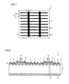
- FIG. 1 A schematic plan view of a solar cell of a first embodiment as seen from its light-receiving surface is shown in Fig. 1 .
- an antireflection film 7 and a light-receiving surface electrode 8 are formed on the light-receiving surface of a p-type silicon substrate 2 of a solar cell 1.
- Antireflection film 7 is made of a silicon nitride film or the like, for example.
- Light-receiving surface electrode 8 is formed of a subgrid electrode 10 and a main grid electrode 11, and subgrid electrode 10 and main grid electrode 11 both have a rectangular surface shape.
- subgrid electrode 10 and the longitudinal direction of main grid electrode 11 make an angle of about 90°, and subgrid electrode 10 crosses main grid electrode 11.
- FIG. 2 A schematic sectional view taken along the line II-II of Fig. 1 is shown in Fig. 2 .
- An uneven structure 3 as a textured structure is formed on the light-receiving surface side of p-type silicon substrate 2
- an n-type impurity diffusion region 4 as an n-type impurity diffusion layer is formed on the light-receiving surface of p-type silicon substrate 2.
- n-type impurity diffusion region 4 has an n-type impurity first diffusion region 5 and an n-type impurity second diffusion region 6.
- the concentration of an n-type impurity in the surface of n-type impurity second diffusion region 6 is higher than the concentration of the n-type impurity in the surface of n-type impurity first diffusion region 5.
- subgrid electrode 10 is formed to come into contact with a part of the surface of n-type impurity second diffusion region 6, and a rear electrode 9 is formed on the rear surface of p-type silicon substrate 2 at the opposite side of the light-receiving surface.
- the thickness of p-type silicon substrate 2 is about 200 ⁇ m, for example, and the width and length of the light-receiving surface of p-type silicon substrate 2 are both about 156.5 mm, for example.
- n-type impurity second diffusion region 6 will have a protruding portion formed along the longitudinal direction of subgrid electrode 10 (the direction normal to the sheet of drawing of Fig. 2 ).
- FIG. 3(a) A schematic plan view of p-type silicon substrate 2 as seen from the light-receiving surface side with antireflection film 7 formed on the light-receiving surface of solar cell 1 having been removed is shown in Fig. 3(a) , and a schematic enlarged plan view of and around an end of subgrid electrode 10 shown in Fig. 3(a) is shown in Fig. 3(b) .
- n-type impurity diffusion region 4 is formed substantially all over the light-receiving surface of p-type silicon substrate 2, and n-type impurity second diffusion regions 6 having a rectangular surface are arranged spaced apart from one another in the form of a plurality of islands.
- subgrid electrode 10 is electrically connected to the plurality of n-type impurity second diffusion regions 6 along a longitudinal direction 10a thereof.
- a length B of n-type impurity second diffusion region 6 in the longitudinal direction be more than or equal to three times and less than or equal to five times a width A representing the length of subgrid electrode 10 in the direction orthogonal to longitudinal direction 10a.
- width A of subgrid electrode 10 can be 100 ⁇ m, for example, and length B of n-type impurity second diffusion region 6 can be 500 ⁇ m, for example.
- n-type impurity second diffusion region 6 is rectangular
- the surface shape of n-type impurity second diffusion region 6 is not limited to the rectangular shape, but may be elliptical, for example.
- p-type silicon substrate 2 whose light-receiving surface has a width and a length of both about 156.5 mm and a thickness of about 200 ⁇ m, for example, is prepared, and uneven structure 3 is formed on the light-receiving surface of p-type silicon substrate 2.
- n-type impurity diffusion region 4 is formed. Since n-type impurity diffusion region 4 is a diffusion layer of phosphorus which is an n-type impurity, the concentration gradient of phosphorus concentration in which the phosphorus concentration gradually decreases from the light-receiving surface of p-type silicon substrate 2 toward the inside is formed. Then, a glass layer formed on the light-receiving surface of p-type silicon substrate 2 when phosphorus is diffused is removed by a hydrofluoric acid treatment.
- the sheet resistance of the light-receiving surface of p-type silicon substrate 2 is measured by a four probe method.
- the sheet resistance of the light-receiving surface of p-type silicon substrate 2 is controlled to fall within the range between more than or equal to 30 ⁇ / and less than or equal to 60 ⁇ / , for example.
- the method for controlling the concentration of the n-type impurity in the surface of n-type impurity diffusion region 4 also includes a method using SIMS (Secondary Ion-microprobe Mass Spectrometry) and the like, the method for measuring the sheet resistance is simple.
- the sheet resistance of the surface of n-type impurity diffusion region 4 is not particularly limited provided that the contact resistance with light-receiving surface electrode 8 to be formed in a subsequent step is sufficiently low, but an optimum value varies depending on the composition, formation conditions, and the like of light-receiving surface electrode 8.
- an acid-resistant mask 51 is formed in a region of the surface of n-type impurity diffusion region 4 where light-receiving surface electrode 8 is to be disposed.
- N-type impurity diffusion region 4 with acid-resistant mask 51 formed thereon will be left as n-type impurity second diffusion region 6 in a subsequent step.
- the method for forming acid-resistant mask 51 includes a method using photolithography, a method using a printing method such as screen printing, or a method using ink jet, for example.
- n-type impurity diffusion region 4 that is not protected by acid-resistant mask 51 is etched, so that n-type impurity first diffusion region 5 whose surface has a sheet resistance of about 90 ⁇ / , for example, is formed.
- a portion of n-type impurity diffusion region 4 that is protected by acid-resistant mask 51 is not etched at this time, and n-type impurity second diffusion region 6 whose surface has a sheet resistance lower than that of the surface of n-type impurity first diffusion region 5 formed by etching is formed. This is because, as described above, the concentration gradient of phosphorous concentration in which the phosphorus concentration gradually decreases from the light-receiving surface of p-type silicon substrate 2 toward the inside is formed.
- acid-resistant mask 51 is removed from p-type silicon substrate 2, and then antireflection film 7 made of a silicon nitride film or the like, for example, is formed on the light-receiving surface of p-type silicon substrate 2.
- light-receiving surface electrode 8 is formed on the light-receiving surface of p-type silicon substrate 2, and rear electrode 9 is formed on the rear surface of p-type silicon substrate 2.
- Light-receiving surface electrode 8 and rear electrode 9 are each formed by, for example, printing a conductive paste by the screen printing method and then firing the conductive paste.
- Light-receiving surface electrode 8 is formed such that a constituent of the conductive paste breaks through antireflection film 7 during firing of the conductive paste to come into contact with n-type impurity second diffusion region 6.
- n-type impurity second diffusion regions 6 are arranged spaced apart from one another, and subgrid electrode 10 of light-receiving surface electrode 8 is connected to the plurality of n-type impurity second diffusion regions 6 in its longitudinal direction.
- n-type impurity second diffusion regions 6 which can suppress a reduction in conversion efficiency that would be caused by a displacement of light-receiving surface electrode 8 of solar cell 1 having, on the light-receiving surface, n-type impurity first diffusion region 5 having a low n-type impurity concentration for suppressing recombination and n-type impurity second diffusion regions 6 having a high n-type impurity concentration for suppressing an increase in contact resistance with light-receiving surface electrode 8.
- FIG. 5(a) A schematic enlarged plan view illustrating the relationship between subgrid electrode 10 and n-type impurity second diffusion regions 6 of the solar cell of the first embodiment is shown in Fig. 5(a) .
- the surface shape of n-type impurity second diffusion region 6 shall be rectangular.
- a crossing rate Z (%) of n-type impurity second diffusion regions 6 relative to subgrid electrode 10 is defined by an expression (I) below.
- Crossing rate Z % 100 ⁇ X / Y
- a length X represents the length of n-type impurity second diffusion regions 6 in longitudinal direction 10a of subgrid electrode 10, as shown in Fig. 5(a) .
- a pitch Y represents the pitch of n-type impurity second diffusion regions 6 between n-type impurity second diffusion regions 6 in longitudinal direction 10a, as shown in Fig. 5(a) .
- n-type impurity second diffusion region 6 is formed to have a surface shape of linear shape in conformity with the surface shape of subgrid electrode 10, width A of subgrid electrode 10 is set at 100 ⁇ m, and a width B of n-type impurity second diffusion region 6 is set at 100 ⁇ m.
- n-type impurity second diffusion region 6 except the region in contact with subgrid electrode 10 increases, recombination of carriers in the light-receiving surface will increase, and the short circuit current density (J sc ) and the open circuit voltage (V oc ) as characteristics of a solar cell will be smaller.
- the reason for setting crossing rate Z at 20% is because it is considered that the J sc value and the V oc value remain equivalent to those of the control when crossing rate Z is set at less than or equal to 20%.
- the E ff value similar to those of the control can be obtained in the case where length X of n-type impurity second diffusion regions 6 in longitudinal direction 10a of subgrid electrode 10 is less than or equal to 50 ⁇ m. Therefore, the E ff value of conversion efficiency equivalent to that of the control can be obtained while maintaining the J sc value and the V oc value and suppressing a reduction in the F.F. value.
- the width of n-type impurity second diffusion regions 6 wider than the width of subgrid electrode 10 to connect subgrid electrode 10 within the width of n-type impurity second diffusion regions 6 as well as arranging a plurality of n-type impurity second diffusion regions 6 spaced apart from one another along longitudinal direction 10a of subgrid electrode 10, it is possible to suppress a reduction in conversion efficiency that would be caused by a displacement of light-receiving surface electrode 8 of solar cell 1 having, on the light-receiving surface, n-type impurity first diffusion region 5 having a low n-type impurity concentration for suppressing recombination and n-type impurity second diffusion regions 6 having a high n-type impurity concentration for suppressing an increase in contact resistance with light-receiving surface electrode 8.
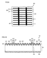
- FIG. 6(a) A schematic plan view of a p-type silicon substrate as seen from the light-receiving surface side with an antireflection film formed on the light-receiving surface of a solar cell of a second embodiment having been removed is shown in Fig. 6(a) , and a schematic enlarged plan view of and around an end of a subgrid electrode is shown in Fig. 6(b) .
- the solar cell of the second embodiment is characterized in that the surface shape of n-type impurity second diffusion region 6 is a shape having a protruding portion 6a protruding in longitudinal direction 10a of subgrid electrode 10 rather than the rectangular shape extended in the direction orthogonal to longitudinal direction 10a of subgrid electrode 10.
- n-type impurity second diffusion regions 6 adjacent to each other in longitudinal direction 10a of subgrid electrode 10 are arranged not to be in contact with each other, subgrid electrode 10 will be connected to a plurality of n-type impurity second diffusion regions 6 having width B wider than width A of subgrid electrode 10 in longitudinal direction 10a thereof.
- width A of subgrid electrode 10 can be 100 ⁇ m, for example, and width B of n-type impurity second diffusion regions 6 can be 500 ⁇ m, for example.
- connection with subgrid electrode 10 can be ensured by other n-type impurity second diffusion regions 6, which can suppress a reduction in conversion efficiency that would be caused by a displacement of light-receiving surface electrode 8 of solar cell 1 having, on the light-receiving surface, n-type impurity first diffusion region 5 having a low n-type impurity concentration for suppressing recombination and n-type impurity second diffusion region 6 having a high n-type impurity concentration for suppressing an increase in contact resistance with light-receiving surface electrode 8.
- FIG. 7(a) A schematic plan view of a p-type silicon substrate as seen from the light-receiving surface side with an antireflection film formed on the light-receiving surface of a solar cell of a third embodiment having been removed is shown in Fig. 7(a) , and a schematic enlarged plan view of and around an end of a subgrid electrode shown in Fig. 7(a) is shown in Fig. 7(b) .
- the solar cell of the third embodiment is characterized in that n-type impurity second diffusion regions 6 are coupled to one another in longitudinal direction 10a of subgrid electrode 10 and that a coupling portion 6b of n-type impurity second diffusion regions 6 has a width C narrower than width A of subgrid electrode 10.
- n-type impurity second diffusion region 6 has a protruding portion 6c protruding in the direction orthogonal to longitudinal direction 10a of subgrid electrode 10.
- subgrid electrode 10 will be connected to n-type impurity second diffusion regions 6 having width B wider than width A of subgrid electrode 10 in longitudinal direction 10a.
- width A of subgrid electrode 10 can be 100 ⁇ m, for example, and width B of n-type impurity second diffusion regions 6 can be 500 ⁇ m, for example.
- connection with subgrid electrode 10 can be ensured by protruding portions 6c of n-type impurity second diffusion regions 6, which can suppress a reduction in conversion efficiency that would be caused by a displacement of light-receiving surface electrode 8 of solar cell 1 having, on the light-receiving surface, n-type impurity first diffusion region 5 having a low n-type impurity concentration for suppressing recombination and n-type impurity second diffusion regions 6 having a high n-type impurity concentration for suppressing an increase in contact resistance with light-receiving surface electrode 8.
- FIG. 8(a) A schematic plan view of a p-type silicon substrate as seen from the light-receiving surface side with an antireflection film formed on the light-receiving surface of a solar cell of a fourth embodiment having been removed is shown in Fig. 8(a) , and a schematic enlarged plan view of and around an end of a subgrid electrode shown in Fig. 8(a) is shown in Fig. 8(b) .
- the solar cell of the fourth embodiment is characterized in that coupling portion 6b coupling n-type impurity second diffusion regions 6 along longitudinal direction 10a of subgrid electrode 10 has a width D wider than width A of subgrid electrode 10.
- subgrid electrode 10 will be connected to n-type impurity second diffusion regions 6 having width B wider than width A of subgrid electrode 10 in longitudinal direction 10a.
- width A of subgrid electrode 10 can be 100 ⁇ m, for example, width B of n-type impurity second diffusion regions 6 can be 500 ⁇ m, for example, width D of coupling portion 6b of n-type impurity second diffusion regions 6 can be 350 ⁇ m, for example, and a width E of protruding portion 6c protruding in the direction orthogonal to longitudinal direction 10a of subgrid electrode 10 can be made narrower than in the third embodiment.
- connection with subgrid electrode 10 can be ensured by protruding portions 6c of n-type impurity second diffusion regions 6, which can suppress a reduction in conversion efficiency that would be caused by a displacement of light-receiving surface electrode 8 of solar cell 1 having, on the light-receiving surface, n-type impurity first diffusion region 5 having a low n-type impurity concentration for suppressing recombination and n-type impurity second diffusion region 6 having a high n-type impurity concentration for suppressing an increase in contact resistance with light-receiving surface electrode 8.
- the diffusion region on the light-receiving surface side will be a p-type impurity diffusion region
- the p-type impurity diffusion region will be made of a p-type impurity first diffusion region and a p-type impurity second diffusion region
- the concentration of a p-type impurity in the surface of the p-type impurity first diffusion region will be lower than the concentration of the p-type impurity in the surface of the p-type impurity second diffusion region.
- the present invention can be applied to a solar cell, and more particularly to a solar cell having, on the light-receiving surface, an impurity diffusion region having a low impurity concentration for suppressing recombination and an impurity diffusion region having a high impurity concentration for suppressing an increase in contact resistance with a light-receiving surface electrode.
Landscapes
- Photovoltaic Devices (AREA)
Abstract
Disclosed is a solar cell (1) wherein a diffusion region (4) containing an impurity of a second conductivity type provided on a light-receiving surface side of a silicon substrate (2) containing an impurity of a first conductivity type has a first diffusion region (5) and second diffusion regions (6). Surfaces of the second diffusion regions (6) are higher in concentration of the impurity of the second conductivity type than a surface of the first diffusion region (5). The second diffusion regions (6) are arranged spaced apart from one another. A light-receiving surface electrode (8) is connected to a plurality of the second diffusion regions (6).
Description
- The present invention relates to a solar cell, and more particularly to a structure of a light-receiving surface side of a solar cell.
- A solar cell is an element that converts solar energy directly into electrical energy. Since the solar cell easily harmonizes with the environment and its energy source is solar energy, it can be said that its energy source is infinite. Furthermore, the solar cell is also advantageous in having a long life. The solar cell includes a crystalline silicon solar cell, a compound semiconductor solar cell, and the like.
-
Fig. 9 is a schematic plan view of a solar cell described in conventional Non-Patent Literature 1 (Thomas Lauermann et al., "INSECT: AN INLINE SELECTIVE EMITTER CONCEPT WITH HIGH EFFICIENCIES AT COMPETITIVE PROCESS COSTS IMPROVED WITH INKJET MASKING TECHNOLOGY.", 24th EU PVSEC Hamburg, September 21-25, 2009) as seen from the light-receiving surface side, andFig. 10 is a schematic sectional view taken along the line X-X ofFig. 9 . As shown inFig. 9 , formed on the light-receiving surface of asolar cell 201 is a light-receivingsurface electrode 208 formed of asubgrid electrode 210 and amain grid electrode 211 crossingsubgrid electrode 210. Anantireflection film 207 is also formed on the light-receiving surface ofsolar cell 201. - Moreover, as shown in
Fig. 10 , anuneven structure 203 as a textured structure is formed on the light-receiving surface of a p-type silicon substrate 202 ofsolar cell 201, and an n-typeimpurity diffusion region 204 is formed all over the light-receiving surface of p-type silicon substrate 202. - N-type
impurity diffusion region 204 has an n-type impurityfirst diffusion region 205 and an n-type impuritysecond diffusion region 206. The concentration of an n-type impurity in the surface of n-type impurityfirst diffusion region 205 is lower than the concentration of the n-type impurity in the surface of n-type impuritysecond diffusion region 206. - The light-receiving surface of n-type
impurity diffusion region 204 is covered withantireflection film 207, andsubgrid electrode 210 is formed to be in contact with n-type impuritysecond diffusion region 206. Arear electrode 209 is formed on the rear surface of p-type silicon substrate 202 on the opposite side of the light-receiving surface. - N-type
impurity diffusion region 204 is formed by doping the light-receiving surface of p-type silicon substrate 202 with the n-type impurity. At this time, from the viewpoint of reducing contact resistance between light-receivingsurface electrode 208 and n-typeimpurity diffusion region 204, it is preferable that the concentration of the n-type impurity in n-typeimpurity diffusion region 204 be high. - On the other hand, from the viewpoint of reducing recombination of electron and hole in the light-receiving surface of
solar cell 201, it is preferable that the concentration of the n-type impurity in n-typeimpurity diffusion region 204 be low. - That is, when the concentration of the n-type impurity in n-type
impurity diffusion region 204 is excessively low, an increase in contact resistance between light-receivingsurface electrode 208 and n-typeimpurity diffusion region 204, namely, an increase in series resistance will be incurred. On the other hand, when a reduction in the concentration of the n-type impurity in n-typeimpurity diffusion region 204 is insufficient, the effect of reducing recombination of electron and hole in the light-receiving surface ofsolar cell 201 will be lowered. - Therefore, in n-type
impurity diffusion region 204, by making the concentration of the n-type impurity in n-type impuritysecond diffusion region 206 as a region in contact with light-receivingsurface electrode 208 higher than that in n-type impurityfirst diffusion region 205 as a remaining region,solar cell 201 is obtained in which recombination of electron and hole in n-type impurityfirst diffusion region 205 is reduced while minimizing contact resistance between light-receivingsurface electrode 208 and n-type impuritysecond diffusion region 206. - NPL 1 also discloses a method for manufacturing
solar cell 201 described above by a simple method that a complicated step, such as photolithography, is not required. - Schematic sectional views illustrating the method for manufacturing
solar cell 201 described inconventional NPL 1 are shown inFigs. 11(a) to 11(f) . Hereinbelow, referring toFigs. 11(a) to 11(f) , the method for manufacturingsolar cell 201 described inconventional NPL 1 will be explained. - First, as shown in
Fig. 11(a) ,uneven structure 203 is formed on a surface on the side to be a light-receiving surface (hereinafter referred to as a "light-receiving surface") of p-type silicon substrate 202. - Next, as shown in
Fig. 11(b) , by vapor phase diffusion using POCl3, phosphorus is diffused into the light-receiving surface of p-type silicon substrate 202 to form n-typeimpurity diffusion region 204. Since n-typeimpurity diffusion region 204 is an impurity diffusion layer, the concentration gradient is formed in which a phosphorus concentration gradually decreases from the light-receiving surface of p-type silicon substrate 202 toward the inside. - Next, as shown in
Fig. 11(c) , an acid-resistant mask 251 is formed in a region of the light-receiving surface of p-type silicon substrate 202 ofuneven structure 203 where light-receivingsurface electrode 208 is to be disposed. - Next, as shown in
Fig. 11(d) , etching is performed on the light-receiving surface side of p-type silicon substrate 202. Accordingly, a portion of n-typeimpurity diffusion region 204 that is not protected by acid-resistant mask 251 is etched to form n-type impurityfirst diffusion region 205. Since a portion of n-typeimpurity diffusion region 204 that is protected by acid-resistant mask 251 is not etched at this time, n-type impuritysecond diffusion region 206 having a surface lower in sheet resistance than the surface of n-type impurityfirst diffusion region 205 is formed. This is because the concentration gradient in which the phosphorus concentration gradually decreases from the light-receiving surface of p-type silicon substrate 202 toward the inside is formed as described above. - Next, as shown in
Fig. 11(e) , acid-resistant mask 251 is removed from the light-receiving surface of p-type silicon substrate 202 to formantireflection film 207 made of a silicon nitride film on the light-receiving surface of p-type silicon substrate 202. - Next, as shown in
Fig. 11(f) , light-receivingsurface electrode 208 is formed to come into contact with n-type impuritysecond diffusion region 206 exposed by removing a part ofantireflection films 207, andrear electrode 209 is formed on the rear surface of p-type silicon substrate 202, thereby formingsolar cell 201. - A schematic plan view of p-
type silicon substrate 202 as seen from the light-receiving surface side withantireflection film 207 formed on the light-receiving surface ofsolar cell 201 described inconventional NPL 1 having been removed is shown inFig. 12(a) , and a schematic enlarged plan view of and around an end ofsubgrid electrode 210 shown inFig. 12(a) is shown inFig. 12(b) . - As shown in
Figs. 12(a) and 12(b) , n-type impuritysecond diffusion region 206 and light-receivingsurface electrode 208 have the same planar shape, however, n-type impuritysecond diffusion region 206 has an area larger than the formation area of light-receivingsurface electrode 208, and light-receivingsurface electrode 208 is formed within n-type impuritysecond diffusion region 206. - NPL 1: Thomas Lauermann et al., "INSECT: AN INLINE SELECTIVE EMITTER CONCEPT WITH HIGH EFFICIENCIES AT COMPETITIVE PROCESS COSTS IMPROVED WITH INKJET MASKING TECHNOLOGY.", 24th EU PVSEC Hamburg, September 21-25, 2009
- As described above, in the method for manufacturing
solar cell 201 ofNPL 1, n-type impurityfirst diffusion region 205 and n-type impuritysecond diffusion region 206 are formed by diffusing phosphorus as an n-type impurity into the light-receiving surface of p-type silicon substrate 202 in a single diffusion step. - However, the method for manufacturing
solar cell 201 ofNPL 1 raises problems in that a displacement of light-receivingsurface electrode 208 relative to n-type impuritysecond diffusion region 206 occurs when forming light-receivingsurface electrode 208, and light-receivingsurface electrode 208 is not formed on n-type impuritysecond diffusion region 206, so that series resistance increases and conversion efficiency is reduced. - In view of the above-described circumstances, the present invention has an object to provide a solar cell capable of suppressing a reduction in conversion efficiency that would be caused by a displacement of a light-receiving surface electrode.
- According to an aspect of the present invention, a solar cell includes a silicon substrate containing an impurity of a first conductivity type, a diffusion region containing an impurity of a second conductivity type provided on a light-receiving surface side of the silicon substrate, and a light-receiving surface electrode provided on the light-receiving surface side of the diffusion region. The diffusion region has a first diffusion region and second diffusion regions. Surfaces of the second diffusion regions are higher in concentration of the impurity of the second conductivity type than a surface of the first diffusion region. The second diffusion regions are arranged spaced apart from one another. The light-receiving surface electrode is connected to a plurality of the second diffusion regions.
- Here, according to an aspect of solar cell of the present invention, the light-receiving surface electrode may be formed of a main grid electrode and a subgrid electrode, and the subgrid electrode may be connected to the plurality of the second diffusion regions.
- According to an aspect of solar cell of the present invention, the subgrid electrode may cross the main grid electrode.
- According to an aspect of solar cell of the present invention, the second diffusion regions may have a rectangular shape.
- According to an aspect of solar cell of the present invention, when a crossing rate Z of the second diffusion regions is expressed by the following expression (I): the crossing rate Z

where X represents a length of the second diffusion regions in a longitudinal direction of the subgrid electrode, and Y represents a pitch between the second diffusion regions in the longitudinal direction of the subgrid electrode, the crossing rate Z of the second diffusion regions may be less than or equal to 20%. - According to an aspect of solar cell of the present invention, the second diffusion regions may each have a protruding portion protruding in the longitudinal direction of the subgrid electrode.
- According to an aspect of the present invention, a solar cell includes a silicon substrate containing an impurity of a first conductivity type, a diffusion region containing an impurity of a second conductivity type provided on a light-receiving surface side of the silicon substrate, and a light-receiving surface electrode provided on the light-receiving surface side of the diffusion region. The diffusion region has a first diffusion region and second diffusion regions. Surfaces of the second diffusion regions are higher in concentration of the impurity of the second conductivity type than a surface of the first diffusion region. The light-receiving surface electrode is formed of a main grid electrode and a subgrid electrode. The second diffusion regions have regions in contact with the subgrid electrode. The second diffusion regions each have a protruding portion protruding in a direction orthogonal to a longitudinal direction of the subgrid electrode.
- According to an aspect of solar cell of the present invention, the subgrid electrode may cross the main grid electrode.
- Furthermore, according to an aspect of solar cell of the present invention, the second conductivity type may be an n-type.
- According to the present invention, a solar cell capable of suppressing a reduction in conversion efficiency that would be caused by a displacement of a light-receiving surface electrode can be provided.
-
-
Fig. 1 is a schematic plan view of a solar cell of a first embodiment as seen from its light-receiving surface. -
Fig. 2 is a schematic sectional view taken along the line II-II ofFig. 1 . -
Fig. 3(a) is a schematic plan view of a p-type silicon substrate as seen from the light-receiving surface side with an antireflection film formed on the light-receiving surface of the solar cell of the first embodiment having been removed, andFig. 3(b) is a schematic enlarged plan view of and around an end of a subgrid electrode shown inFig. 3(a) . -
Figs. 4(a) to (f) are schematic sectional views illustrating an example of a method for manufacturing the solar cell of the first embodiment. -
Fig. 5(a) is a schematic enlarged plan view illustrating the relationship between the subgrid electrode and n-type impurity second diffusion regions of the solar cell of the first embodiment, andFig. 5(b) is a schematic enlarged plan view illustrating the relationship between a subgrid electrode and n-type impurity second diffusion regions of a solar cell of a control. -
Fig. 6(a) is a schematic plan view of a p-type silicon substrate as seen from the light-receiving surface side with an antireflection film formed on the light-receiving surface of a solar cell of a second embodiment having been removed, andFig. 6(b) is a schematic enlarged plan view of and around an end of a subgrid electrode shown inFig. 6(a) . -
Fig. 7(a) is a schematic plan view of a p-type silicon substrate as seen from the light-receiving surface side with an antireflection film formed on the light-receiving surface of a solar cell of a third embodiment having been removed, andFig. 7(b) is a schematic enlarged plan view of and around an end of a subgrid electrode shown inFig. 7(a) . -
Fig. 8(a) is a schematic plan view of a p-type silicon substrate as seen from the light-receiving surface side with an antireflection film formed on the light-receiving surface of a solar cell of a fourth embodiment having been removed, andFig. 8(b) is a schematic enlarged plan view of and around an end of a subgrid electrode shown inFig. 8(a) . -
Fig. 9 is a schematic plan view of a conventional solar cell described inNPL 1 as seen from the light-receiving surface side. -
Fig. 10 is a schematic sectional view taken along the line X-X ofFig. 9 . -
Figs. 11 (a) to (f) are schematic sectional views illustrating a method for manufacturing the conventional solar cell described inNPL 1. -
Fig. 12(a) is a schematic plan view of a p-type silicon substrate as seen from the light-receiving surface side with an antireflection film formed on the light-receiving surface of the conventional solar cell described inNPL 1 having been removed, andFig. 12(b) is a schematic enlarged plan view of and around an end of a subgrid electrode shown inFig. 12(a) . - Hereinbelow, embodiments of the present invention will be described. It is noted that, in the drawings of the present invention, the same reference character shall represent the same portion or a corresponding portion.
- A schematic plan view of a solar cell of a first embodiment as seen from its light-receiving surface is shown in
Fig. 1 . As shown inFig. 1 , anantireflection film 7 and a light-receivingsurface electrode 8 are formed on the light-receiving surface of a p-type silicon substrate 2 of asolar cell 1.Antireflection film 7 is made of a silicon nitride film or the like, for example. Light-receivingsurface electrode 8 is formed of asubgrid electrode 10 and amain grid electrode 11, andsubgrid electrode 10 andmain grid electrode 11 both have a rectangular surface shape. - Here, the longitudinal direction of
subgrid electrode 10 and the longitudinal direction ofmain grid electrode 11 make an angle of about 90°, andsubgrid electrode 10 crossesmain grid electrode 11. - A schematic sectional view taken along the line II-II of
Fig. 1 is shown inFig. 2 . Anuneven structure 3 as a textured structure is formed on the light-receiving surface side of p-type silicon substrate 2, and an n-typeimpurity diffusion region 4 as an n-type impurity diffusion layer is formed on the light-receiving surface of p-type silicon substrate 2. Here, n-typeimpurity diffusion region 4 has an n-type impurityfirst diffusion region 5 and an n-type impuritysecond diffusion region 6. The concentration of an n-type impurity in the surface of n-type impuritysecond diffusion region 6 is higher than the concentration of the n-type impurity in the surface of n-type impurityfirst diffusion region 5. - In addition,
subgrid electrode 10 is formed to come into contact with a part of the surface of n-type impuritysecond diffusion region 6, and arear electrode 9 is formed on the rear surface of p-type silicon substrate 2 at the opposite side of the light-receiving surface. It is noted that the thickness of p-type silicon substrate 2 is about 200 µm, for example, and the width and length of the light-receiving surface of p-type silicon substrate 2 are both about 156.5 mm, for example. - Furthermore, since the thickness of p-
type silicon substrate 2 in n-type impuritysecond diffusion region 6 is thicker than the thickness of p-type silicon substrate 2 in n-type impurityfirst diffusion region 5, n-type impuritysecond diffusion region 6 will have a protruding portion formed along the longitudinal direction of subgrid electrode 10 (the direction normal to the sheet of drawing ofFig. 2 ). - A schematic plan view of p-
type silicon substrate 2 as seen from the light-receiving surface side withantireflection film 7 formed on the light-receiving surface ofsolar cell 1 having been removed is shown inFig. 3(a) , and a schematic enlarged plan view of and around an end ofsubgrid electrode 10 shown inFig. 3(a) is shown inFig. 3(b) . - As shown in
Fig. 3(a) , n-typeimpurity diffusion region 4 is formed substantially all over the light-receiving surface of p-type silicon substrate 2, and n-type impuritysecond diffusion regions 6 having a rectangular surface are arranged spaced apart from one another in the form of a plurality of islands. - As shown in
Fig. 3(b) ,subgrid electrode 10 is electrically connected to the plurality of n-type impuritysecond diffusion regions 6 along alongitudinal direction 10a thereof. - Here, it is preferable that a length B of n-type impurity
second diffusion region 6 in the longitudinal direction be more than or equal to three times and less than or equal to five times a width A representing the length ofsubgrid electrode 10 in the direction orthogonal tolongitudinal direction 10a. In this case, by suppressing an increase in the formation area of n-type impuritysecond diffusion regions 6 while ensuring electric connection between n-type impuritysecond diffusion regions 6 andsubgrid electrode 10, recombination of electron and hole in the light-receiving surface ofsolar cell 1 can be reduced, so that a reduction in conversion efficiency ofsolar cell 1 can be suppressed. - It is noted that width A of
subgrid electrode 10 can be 100 µm, for example, and length B of n-type impuritysecond diffusion region 6 can be 500 µm, for example. - Although the case where the surface shape of n-type impurity
second diffusion region 6 is rectangular has been described above, the surface shape of n-type impuritysecond diffusion region 6 is not limited to the rectangular shape, but may be elliptical, for example. - Referring to schematic sectional views of
Figs. 4(a) to 4(f) , an example of the method for manufacturingsolar cell 1 of the first embodiment will be described below. - First, as shown in
Fig. 4(a) , p-type silicon substrate 2 whose light-receiving surface has a width and a length of both about 156.5 mm and a thickness of about 200 µm, for example, is prepared, anduneven structure 3 is formed on the light-receiving surface of p-type silicon substrate 2. - Next, as shown in
Fig. 4(b) , by performing vapor phase diffusion of phosphorus into the light-receiving surface of p-type silicon substrate 2 using POCl3, n-typeimpurity diffusion region 4 is formed. Since n-typeimpurity diffusion region 4 is a diffusion layer of phosphorus which is an n-type impurity, the concentration gradient of phosphorus concentration in which the phosphorus concentration gradually decreases from the light-receiving surface of p-type silicon substrate 2 toward the inside is formed. Then, a glass layer formed on the light-receiving surface of p-type silicon substrate 2 when phosphorus is diffused is removed by a hydrofluoric acid treatment. - Next, for concentration control of the n-type impurity in the surface of n-type
impurity diffusion region 4, the sheet resistance of the light-receiving surface of p-type silicon substrate 2 is measured by a four probe method. Here, the sheet resistance of the light-receiving surface of p-type silicon substrate 2 is controlled to fall within the range between more than or equal to 30Ω/ and less than or equal to 60 Ω/ , for example. Although the method for controlling the concentration of the n-type impurity in the surface of n-typeimpurity diffusion region 4 also includes a method using SIMS (Secondary Ion-microprobe Mass Spectrometry) and the like, the method for measuring the sheet resistance is simple. - The sheet resistance of the surface of n-type
impurity diffusion region 4 is not particularly limited provided that the contact resistance with light-receivingsurface electrode 8 to be formed in a subsequent step is sufficiently low, but an optimum value varies depending on the composition, formation conditions, and the like of light-receivingsurface electrode 8. - Next, as shown in
Fig. 4(c) , an acid-resistant mask 51 is formed in a region of the surface of n-typeimpurity diffusion region 4 where light-receivingsurface electrode 8 is to be disposed. N-typeimpurity diffusion region 4 with acid-resistant mask 51 formed thereon will be left as n-type impuritysecond diffusion region 6 in a subsequent step. The method for forming acid-resistant mask 51 includes a method using photolithography, a method using a printing method such as screen printing, or a method using ink jet, for example. - Next, as shown in
Fig. 4(d) , the light-receiving surface of p-type silicon substrate 2 is etched. Accordingly, a portion of n-typeimpurity diffusion region 4 that is not protected by acid-resistant mask 51 is etched, so that n-type impurityfirst diffusion region 5 whose surface has a sheet resistance of about 90 Ω/ , for example, is formed. A portion of n-typeimpurity diffusion region 4 that is protected by acid-resistant mask 51 is not etched at this time, and n-type impuritysecond diffusion region 6 whose surface has a sheet resistance lower than that of the surface of n-type impurityfirst diffusion region 5 formed by etching is formed. This is because, as described above, the concentration gradient of phosphorous concentration in which the phosphorus concentration gradually decreases from the light-receiving surface of p-type silicon substrate 2 toward the inside is formed. - Next, as shown in
Fig. 4(e) , acid-resistant mask 51 is removed from p-type silicon substrate 2, and then antireflectionfilm 7 made of a silicon nitride film or the like, for example, is formed on the light-receiving surface of p-type silicon substrate 2. - Next, as shown in
Fig. 4(f) , light-receivingsurface electrode 8 is formed on the light-receiving surface of p-type silicon substrate 2, andrear electrode 9 is formed on the rear surface of p-type silicon substrate 2. Light-receivingsurface electrode 8 andrear electrode 9 are each formed by, for example, printing a conductive paste by the screen printing method and then firing the conductive paste. Light-receivingsurface electrode 8 is formed such that a constituent of the conductive paste breaks throughantireflection film 7 during firing of the conductive paste to come into contact with n-type impuritysecond diffusion region 6. - Then, the four sides of p-
type silicon substrate 2 are cut off by a dicer or the like to achieve junction isolation, so thatsolar cell 1 of the first embodiment is formed. - In
solar cell 1 of the first embodiment having the structure as described above, n-type impuritysecond diffusion regions 6 are arranged spaced apart from one another, andsubgrid electrode 10 of light-receivingsurface electrode 8 is connected to the plurality of n-type impuritysecond diffusion regions 6 in its longitudinal direction. Therefore, even if a displacement occurs between one n-type impuritysecond diffusion region 6 andsubgrid electrode 10, connection withsubgrid electrode 10 can be ensured by other n-type impuritysecond diffusion regions 6, which can suppress a reduction in conversion efficiency that would be caused by a displacement of light-receivingsurface electrode 8 ofsolar cell 1 having, on the light-receiving surface, n-type impurityfirst diffusion region 5 having a low n-type impurity concentration for suppressing recombination and n-type impuritysecond diffusion regions 6 having a high n-type impurity concentration for suppressing an increase in contact resistance with light-receivingsurface electrode 8. - Next, in
solar cell 1 of the first embodiment, in order to suppress recombination of carriers in the light-receiving surface while reducing the contact resistance betweensubgrid electrode 10 and n-type impuritysecond diffusion regions 6, characteristics evaluations of the solar cell were conducted with n-type impuritysecond diffusion regions 6 arranged spaced apart from one another and the length and pitch of n-type impuritysecond diffusion regions 6 varied. - A schematic enlarged plan view illustrating the relationship between
subgrid electrode 10 and n-type impuritysecond diffusion regions 6 of the solar cell of the first embodiment is shown inFig. 5(a) . Here, the surface shape of n-type impuritysecond diffusion region 6 shall be rectangular. - Here, a crossing rate Z (%) of n-type impurity
second diffusion regions 6 relative tosubgrid electrode 10 is defined by an expression (I) below.
- In expression (I) above, a length X represents the length of n-type impurity
second diffusion regions 6 inlongitudinal direction 10a ofsubgrid electrode 10, as shown inFig. 5(a) . A pitch Y represents the pitch of n-type impuritysecond diffusion regions 6 between n-type impuritysecond diffusion regions 6 inlongitudinal direction 10a, as shown inFig. 5(a) . - Moreover, as a control, as shown in
Fig. 5(b) , n-type impuritysecond diffusion region 6 is formed to have a surface shape of linear shape in conformity with the surface shape ofsubgrid electrode 10, width A ofsubgrid electrode 10 is set at 100 µm, and a width B of n-type impuritysecond diffusion region 6 is set at 100 µm. - As the area of n-type impurity
second diffusion region 6 except the region in contact withsubgrid electrode 10 increases, recombination of carriers in the light-receiving surface will increase, and the short circuit current density (Jsc) and the open circuit voltage (Voc) as characteristics of a solar cell will be smaller. - Then, first, in
Fig. 5(a) , the area of n-type impuritysecond diffusion regions 6 except the region in contact withsubgrid electrode 10 was reduced, and crossing rate Z at which the short circuit current density and the open circuit voltage approached those of the control shown inFig. 5(b) was calculated. - Here, results of evaluations of characteristics of the solar cell obtained in the case where pitch Y was kept constant at 1 mm and crossing rate Z was lowered are shown in Table 1. It is noted that F.F. represents the fill factor and Eff represents the conversion efficiency. The Jsc value, the Voc value, the F.F. value, and the Eff value of the control are each set at 1.000. Sample No. 1 has length X of 500 µm (crossing rate Z: 50%), sample No. 2 has length X of 350 µm (crossing rate Z: 35%), and sample No. 3 has length X of 200 µm (crossing rate Z: 20%).
[Table 1] Sample No. Condition (pitch Y: 1mm) Jsc Voc F.F. E ff1 length X: 500µm (=crossing rate Z: 50%) 0.994 0.998 1.003 0.995 2 length X: 350µm (=crossing rate Z: 35%) 0.995 0.998 0.990 0.983 3 length X: 200µm (=crossing rate Z: 20%) 1.000 0.999 0.979 0.980 Control 1.000 1.000 1.000 1.000 - As shown in Table 1, as crossing rate Z was lowered, that is, length X was decreased, the Jsc value and the Voc value were increased, so that the result approaching the control was obtained. On the other hand, in that result, the F.F. value decreased and the influence of the F.F. value was reflected greatly in the Eff value.
- This is considered because, although recombination of carriers in the light-receiving surface could be reduced and the Jsc value and the Voc value could be increased by reducing the area of n-type impurity
second diffusion regions 6 except the region in contact withsubgrid electrode 10, a reduction in the area of n-type impuritysecond diffusion regions 6 in contact withsubgrid electrode 10 caused the increased contact resistance betweensubgrid electrode 10 and n-type impuritysecond diffusion regions 6, resulting in a decrease in the F.F. value. - From the results shown in Table 1, a result was obtained in which the Jsc value and the Voc value were substantially equivalent to those of the control when crossing rate Z was set at 20%. Then, a study for setting crossing rate Z at 20% to bring the F.F. value closer to that of the control was conducted.
- Here, the reason for setting crossing rate Z at 20% is because it is considered that the Jsc value and the Voc value remain equivalent to those of the control when crossing rate Z is set at less than or equal to 20%.
- Next, results of evaluations of characteristics of the solar cell obtained when crossing rate Z was kept constant at 20% and length X and pitch Y were decreased are shown in Table 2. Sample No. 3 has length X of 200 µm similarly to Table 1, sample No. 4 has length X of 100 µm, sample No. 5 has length X of 50 µm, and sample No. 6 has length X of 30 µm.
[Table 2] Sample No. Condition (crossing rate Z: 20%) Jsc Voc F.F. E ff3 length X: 200µm 1.000 0.999 0.979 0.980 4 length X: 100µm 1.000 1.000 0.991 0.993 5 length X: 50µm 1.000 1.000 1.000 1.000 6 length X: 30µm 1.000 1.000 1.000 1.000 Control 1.000 1.000 1.000 1.000 - As shown in Table 2, in samples No. 5 and No. 6, values equivalent to those of the control were obtained for all of the Jsc value, the Voc value, the F.F. value, and the Eff value. Therefore, the results shown in Table 2 reveal that, as shown in
Fig. 5(a) , in the structure in which the surface shape of n-type impuritysecond diffusion regions 6 is rectangular, the longitudinal direction of n-type impuritysecond diffusion regions 6 crosseslongitudinal direction 10a ofsubgrid electrode 10, and further, n-type impuritysecond diffusion regions 6 are arranged at predetermined pitch Y alonglongitudinal direction 10a, the Jsc value, the Voc value, the F.F. value, and the Eff value similar to those of the control can be obtained in the case where length X of n-type impuritysecond diffusion regions 6 inlongitudinal direction 10a ofsubgrid electrode 10 is less than or equal to 50 µm. Therefore, the Eff value of conversion efficiency equivalent to that of the control can be obtained while maintaining the Jsc value and the Voc value and suppressing a reduction in the F.F. value. - As described above, in the solar cell of the first embodiment, by making the width of n-type impurity
second diffusion regions 6 wider than the width ofsubgrid electrode 10 to connectsubgrid electrode 10 within the width of n-type impuritysecond diffusion regions 6 as well as arranging a plurality of n-type impuritysecond diffusion regions 6 spaced apart from one another alonglongitudinal direction 10a ofsubgrid electrode 10, it is possible to suppress a reduction in conversion efficiency that would be caused by a displacement of light-receivingsurface electrode 8 ofsolar cell 1 having, on the light-receiving surface, n-type impurityfirst diffusion region 5 having a low n-type impurity concentration for suppressing recombination and n-type impuritysecond diffusion regions 6 having a high n-type impurity concentration for suppressing an increase in contact resistance with light-receivingsurface electrode 8. - A schematic plan view of a p-type silicon substrate as seen from the light-receiving surface side with an antireflection film formed on the light-receiving surface of a solar cell of a second embodiment having been removed is shown in
Fig. 6(a) , and a schematic enlarged plan view of and around an end of a subgrid electrode is shown inFig. 6(b) . - Here, as shown in
Fig. 6(b) , the solar cell of the second embodiment is characterized in that the surface shape of n-type impuritysecond diffusion region 6 is a shape having a protrudingportion 6a protruding inlongitudinal direction 10a ofsubgrid electrode 10 rather than the rectangular shape extended in the direction orthogonal tolongitudinal direction 10a ofsubgrid electrode 10. - In the solar cell of the second embodiment as well, as shown in
Fig. 6(b) , since n-type impuritysecond diffusion regions 6 adjacent to each other inlongitudinal direction 10a ofsubgrid electrode 10 are arranged not to be in contact with each other,subgrid electrode 10 will be connected to a plurality of n-type impuritysecond diffusion regions 6 having width B wider than width A ofsubgrid electrode 10 inlongitudinal direction 10a thereof. Here, width A ofsubgrid electrode 10 can be 100 µm, for example, and width B of n-type impuritysecond diffusion regions 6 can be 500 µm, for example. - Therefore, in the solar cell of the second embodiment as well, even if a displacement occurs between one n-type impurity
second diffusion region 6 andsubgrid electrode 10, connection withsubgrid electrode 10 can be ensured by other n-type impuritysecond diffusion regions 6, which can suppress a reduction in conversion efficiency that would be caused by a displacement of light-receivingsurface electrode 8 ofsolar cell 1 having, on the light-receiving surface, n-type impurityfirst diffusion region 5 having a low n-type impurity concentration for suppressing recombination and n-type impuritysecond diffusion region 6 having a high n-type impurity concentration for suppressing an increase in contact resistance with light-receivingsurface electrode 8. - The description of the present embodiment except the above is similar to that of the first embodiment, and description thereof will not be repeated.
- A schematic plan view of a p-type silicon substrate as seen from the light-receiving surface side with an antireflection film formed on the light-receiving surface of a solar cell of a third embodiment having been removed is shown in
Fig. 7(a) , and a schematic enlarged plan view of and around an end of a subgrid electrode shown inFig. 7(a) is shown inFig. 7(b) . - As shown in
Fig. 7(b) , the solar cell of the third embodiment is characterized in that n-type impuritysecond diffusion regions 6 are coupled to one another inlongitudinal direction 10a ofsubgrid electrode 10 and that acoupling portion 6b of n-type impuritysecond diffusion regions 6 has a width C narrower than width A ofsubgrid electrode 10. - In addition, in the solar cell of the third embodiment, as shown in
Fig. 7(b) , n-type impuritysecond diffusion region 6 has a protrudingportion 6c protruding in the direction orthogonal tolongitudinal direction 10a ofsubgrid electrode 10. - In the solar cell of the third embodiment, as shown in
Fig. 7(b) ,subgrid electrode 10 will be connected to n-type impuritysecond diffusion regions 6 having width B wider than width A ofsubgrid electrode 10 inlongitudinal direction 10a. Here, width A ofsubgrid electrode 10 can be 100 µm, for example, and width B of n-type impuritysecond diffusion regions 6 can be 500 µm, for example. - Therefore, in the solar cell of the second embodiment as well, even if a displacement occurs between
coupling portions 6b of n-type impuritysecond diffusion regions 6 andsubgrid electrode 10, connection withsubgrid electrode 10 can be ensured by protrudingportions 6c of n-type impuritysecond diffusion regions 6, which can suppress a reduction in conversion efficiency that would be caused by a displacement of light-receivingsurface electrode 8 ofsolar cell 1 having, on the light-receiving surface, n-type impurityfirst diffusion region 5 having a low n-type impurity concentration for suppressing recombination and n-type impuritysecond diffusion regions 6 having a high n-type impurity concentration for suppressing an increase in contact resistance with light-receivingsurface electrode 8. - The description of the present embodiment except the above is similar to those of the first and second embodiments, and description thereof will not be repeated.
- A schematic plan view of a p-type silicon substrate as seen from the light-receiving surface side with an antireflection film formed on the light-receiving surface of a solar cell of a fourth embodiment having been removed is shown in
Fig. 8(a) , and a schematic enlarged plan view of and around an end of a subgrid electrode shown inFig. 8(a) is shown inFig. 8(b) . - The solar cell of the fourth embodiment is characterized in that
coupling portion 6b coupling n-type impuritysecond diffusion regions 6 alonglongitudinal direction 10a ofsubgrid electrode 10 has a width D wider than width A ofsubgrid electrode 10. - In the solar cell of the fourth embodiment, as shown in
Fig. 8(b) ,subgrid electrode 10 will be connected to n-type impuritysecond diffusion regions 6 having width B wider than width A ofsubgrid electrode 10 inlongitudinal direction 10a. Here, width A ofsubgrid electrode 10 can be 100 µm, for example, width B of n-type impuritysecond diffusion regions 6 can be 500 µm, for example, width D ofcoupling portion 6b of n-type impuritysecond diffusion regions 6 can be 350 µm, for example, and a width E of protrudingportion 6c protruding in the direction orthogonal tolongitudinal direction 10a ofsubgrid electrode 10 can be made narrower than in the third embodiment. - Therefore, in the solar cell of the fourth embodiment as well, even if a displacement occurs between
coupling portions 6b of n-type impuritysecond diffusion regions 6 andsubgrid electrode 10, connection withsubgrid electrode 10 can be ensured by protrudingportions 6c of n-type impuritysecond diffusion regions 6, which can suppress a reduction in conversion efficiency that would be caused by a displacement of light-receivingsurface electrode 8 ofsolar cell 1 having, on the light-receiving surface, n-type impurityfirst diffusion region 5 having a low n-type impurity concentration for suppressing recombination and n-type impuritysecond diffusion region 6 having a high n-type impurity concentration for suppressing an increase in contact resistance with light-receivingsurface electrode 8. - The description of the present embodiment except the above is similar to those of the first to third embodiments, and description thereof will not be repeated.
- It is noted that, although the above first to fourth embodiments have described the case where p-
type silicon substrate 2 is used, it is also possible to use an n-type silicon substrate instead of p-type silicon substrate 2. When the n-type silicon substrate is used, the diffusion region on the light-receiving surface side will be a p-type impurity diffusion region, the p-type impurity diffusion region will be made of a p-type impurity first diffusion region and a p-type impurity second diffusion region, and the concentration of a p-type impurity in the surface of the p-type impurity first diffusion region will be lower than the concentration of the p-type impurity in the surface of the p-type impurity second diffusion region. - It should be understood that the embodiments disclosed herein are illustrative and non-restrictive in every respect. The scope of the present invention is defined by the claims not by the description above, and is intended to include any modification within the meaning and scope equivalent to the terms of the claims.
- The present invention can be applied to a solar cell, and more particularly to a solar cell having, on the light-receiving surface, an impurity diffusion region having a low impurity concentration for suppressing recombination and an impurity diffusion region having a high impurity concentration for suppressing an increase in contact resistance with a light-receiving surface electrode.
- 1 solar cell; 2 p-type silicon substrate; 3 uneven structure; 4 n-type impurity diffusion region; 5 n-type impurity first diffusion region; 6 n-type impurity second diffusion region; 6a, 6c protruding portion; 6b coupling portion; 7 antireflection film; 8 light-receiving surface electrode; 9 rear electrode; 10 subgrid electrode; 10a longitudinal direction; 51 acid-resistant mask; 201 solar cell; 202 p-type silicon substrate; 203 uneven structure; 204 n-type impurity diffusion region; 205 n-type impurity first diffusion region; 206 n-type impurity second diffusion region; 207 antireflection film; 208 light-receiving surface electrode; 209 rear electrode; 210 subgrid electrode; 211 main grid electrode; 251 acid-resistant mask.
Claims (9)
- A solar cell (1) comprising:a silicon substrate (2) containing an impurity of a first conductivity type;a diffusion region (4) containing an impurity of a second conductivity type provided on a light-receiving surface side of said silicon substrate (2); anda light-receiving surface electrode (8) provided on the light-receiving surface side of said diffusion region (4), whereinsaid diffusion region (4) has a first diffusion region (5) and second diffusion regions (6),surfaces of said second diffusion regions (6) are higher in concentration of the impurity of said second conductivity type than a surface of said first diffusion region (5),said second diffusion regions (6) are arranged spaced apart from one another, andsaid light-receiving surface electrode (8) is connected to a plurality of said second diffusion regions (6).
- The solar cell (1) according to claim 1, wherein
said light-receiving surface electrode (8) is formed of a main grid electrode (11) and a subgrid electrode (10), and
said subgrid electrode (10) is connected to the plurality of said second diffusion regions (6). - The solar cell (1) according to claim 2, wherein said subgrid electrode (10) crosses said main grid electrode (11).
- The solar cell (1) according to any one of claims 1 to 3, wherein said second diffusion regions (6) have a rectangular shape.
- The solar cell (1) according to claim 4, wherein, when a crossing rate Z of said second diffusion regions (6) is expressed by the following expression (I):

where X represents a length of said second diffusion regions (6) in a longitudinal direction of said subgrid electrode (10), and Y represents a pitch between said second diffusion regions (6) in the longitudinal direction of said subgrid electrode (10),
said crossing rate Z of said second diffusion regions (6) is less than or equal to 20%. - The solar cell (1) according to claim 4 or 5, wherein said second diffusion regions (6) each have a protruding portion (6a) protruding in a longitudinal direction of said subgrid electrode (10).
- A solar cell (1) comprising:a silicon substrate (2) containing an impurity of a first conductivity type;a diffusion region (4) containing an impurity of a second conductivity type provided on a light-receiving surface side of said silicon substrate (2); anda light-receiving surface electrode (8) provided on the light-receiving surface side of said diffusion region (4), whereinsaid diffusion region (4) has a first diffusion region (5) and second diffusion regions (6),surfaces of said second diffusion regions (6) are higher in concentration of the impurity of said second conductivity type than a surface of said first diffusion region (5),said light-receiving surface electrode (8) is formed of a main grid electrode (11) and a subgrid electrode (10),said second diffusion regions (6) have regions in contact with said subgrid electrode (10), andsaid second diffusion regions (6) each have a protruding portion (6c) protruding in a direction orthogonal to a longitudinal direction of said subgrid electrode (10).
- The solar cell (1) according to claim 7, wherein said subgrid electrode (10) crosses said main grid electrode (11).
- The solar cell (1) according to any one of claims 1 to 8, wherein said second conductivity type is an n-type.
Applications Claiming Priority (2)
| Application Number | Priority Date | Filing Date | Title |
|---|---|---|---|
| JP2010143249A JP2012009578A (en) | 2010-06-24 | 2010-06-24 | Solar cell |
| PCT/JP2011/064048 WO2011162203A1 (en) | 2010-06-24 | 2011-06-20 | Solar cell |
Publications (1)
| Publication Number | Publication Date |
|---|---|
| EP2587548A1 true EP2587548A1 (en) | 2013-05-01 |
Family
ID=45371386
Family Applications (1)
| Application Number | Title | Priority Date | Filing Date |
|---|---|---|---|
| EP11798087.0A Withdrawn EP2587548A1 (en) | 2010-06-24 | 2011-06-20 | Solar cell |
Country Status (5)
| Country | Link |
|---|---|
| US (1) | US20130098434A1 (en) |
| EP (1) | EP2587548A1 (en) |
| JP (1) | JP2012009578A (en) |
| CN (1) | CN103069573A (en) |
| WO (1) | WO2011162203A1 (en) |
Cited By (1)
| Publication number | Priority date | Publication date | Assignee | Title |
|---|---|---|---|---|
| WO2013084050A3 (en) * | 2011-12-05 | 2013-12-27 | Centrotherm Photovoltaics Ag | Solar cell having multi-stage doping, and method for producing said solar cell |
Families Citing this family (8)
| Publication number | Priority date | Publication date | Assignee | Title |
|---|---|---|---|---|
| JP2015130367A (en) * | 2012-04-24 | 2015-07-16 | 三菱電機株式会社 | Solar cell and manufacturing method therefor |
| KR20140126819A (en) * | 2013-04-22 | 2014-11-03 | 엘지전자 주식회사 | Solar cell |
| JP2015005621A (en) * | 2013-06-20 | 2015-01-08 | 株式会社ノリタケカンパニーリミテド | Solar cell substrate and manufacturing method thereof |
| JP6422426B2 (en) * | 2014-12-09 | 2018-11-14 | 三菱電機株式会社 | Solar cell |
| JP6395941B2 (en) * | 2015-08-07 | 2018-09-26 | 三菱電機株式会社 | Solar cell and method for manufacturing solar cell |
| JP6614348B2 (en) * | 2016-07-04 | 2019-12-04 | 三菱電機株式会社 | Solar cell evaluation substrate and solar cell evaluation method |
| CN110718598A (en) * | 2019-10-29 | 2020-01-21 | 无锡尚德太阳能电力有限公司 | Cells that prevent the front and rear back electrodes from shifting after welding |
| JP7168800B1 (en) | 2021-12-09 | 2022-11-09 | ジョジアン ジンコ ソーラー カンパニー リミテッド | Solar cells and photovoltaic modules |
Family Cites Families (8)
| Publication number | Priority date | Publication date | Assignee | Title |
|---|---|---|---|---|
| JP2732524B2 (en) * | 1987-07-08 | 1998-03-30 | 株式会社日立製作所 | Photoelectric conversion device |
| DE19522539C2 (en) * | 1995-06-21 | 1997-06-12 | Fraunhofer Ges Forschung | Solar cell with an emitter having a surface texture and method for producing the same |
| JP3781600B2 (en) * | 2000-01-18 | 2006-05-31 | シャープ株式会社 | Solar cell |
| JP3838911B2 (en) * | 2001-12-25 | 2006-10-25 | 京セラ株式会社 | Method for manufacturing solar cell element |
| JP4660642B2 (en) * | 2003-10-17 | 2011-03-30 | 信越化学工業株式会社 | Solar cell and manufacturing method thereof |
| US20080092944A1 (en) * | 2006-10-16 | 2008-04-24 | Leonid Rubin | Semiconductor structure and process for forming ohmic connections to a semiconductor structure |
| JP5344872B2 (en) * | 2008-08-27 | 2013-11-20 | 三菱電機株式会社 | Photovoltaic device |
| KR100997669B1 (en) * | 2008-11-04 | 2010-12-02 | 엘지전자 주식회사 | Silicon solar cell using screen printing method and its manufacturing method |
-
2010
- 2010-06-24 JP JP2010143249A patent/JP2012009578A/en active Pending
-
2011
- 2011-06-20 WO PCT/JP2011/064048 patent/WO2011162203A1/en not_active Ceased
- 2011-06-20 CN CN2011800400530A patent/CN103069573A/en active Pending
- 2011-06-20 EP EP11798087.0A patent/EP2587548A1/en not_active Withdrawn
- 2011-06-20 US US13/806,932 patent/US20130098434A1/en not_active Abandoned
Non-Patent Citations (1)
| Title |
|---|
| See references of WO2011162203A1 * |
Cited By (1)
| Publication number | Priority date | Publication date | Assignee | Title |
|---|---|---|---|---|
| WO2013084050A3 (en) * | 2011-12-05 | 2013-12-27 | Centrotherm Photovoltaics Ag | Solar cell having multi-stage doping, and method for producing said solar cell |
Also Published As
| Publication number | Publication date |
|---|---|
| JP2012009578A (en) | 2012-01-12 |
| WO2011162203A1 (en) | 2011-12-29 |
| CN103069573A (en) | 2013-04-24 |
| US20130098434A1 (en) | 2013-04-25 |
Similar Documents
| Publication | Publication Date | Title |
|---|---|---|
| EP2587548A1 (en) | Solar cell | |
| US8481105B2 (en) | Solar battery and manufacturing method therefor | |
| US20160197207A1 (en) | Solar cell, solar cell module, and manufacturing method of solar cell | |
| EP1887633B2 (en) | Solar cell and solar cell manufacturing method | |
| US20220310858A1 (en) | Back Contact Type Solar Cell Module and Preparation Method | |
| US8936949B2 (en) | Solar cell and manufacturing method thereof | |
| JP2015130527A (en) | Solar battery and manufacturing method of the same | |
| KR100953618B1 (en) | Solar cell | |
| EP4661628A1 (en) | Back-contact cell and photovoltaic module | |
| JP5889163B2 (en) | Photovoltaic device, manufacturing method thereof, and photovoltaic module | |
| KR20140126819A (en) | Solar cell | |
| US20100184250A1 (en) | Self-aligned selective emitter formed by counterdoping | |
| US20130104974A1 (en) | Solar cell and manufacturing method thereof | |
| JP6207414B2 (en) | Photovoltaic element and manufacturing method thereof | |
| KR101153377B1 (en) | Back junction solar cell having improved rear structure and method for manufacturing therof | |
| US9252305B2 (en) | Photovoltaic device, manufacturing method thereof, and photovoltaic module | |
| JP2015162483A (en) | Solar battery cell, solar battery sub cell and solar battery module | |
| KR101135589B1 (en) | Solar Cell | |
| CN210403737U (en) | Silicon controlled rectifier device | |
| CN118367053A (en) | A method for manufacturing a double-sided photovoltaic cell structure | |
| EP3361515B1 (en) | Highly efficient rear-surface electrode type solar cell, solar cell module, and solar power generation system | |
| KR102570365B1 (en) | High photoelectric conversion efficiency solar cell and manufacturing method of high photoelectric conversion efficiency solar cell | |
| KR20120082664A (en) | Method for manufacturing solar cell | |
| EP4646063A1 (en) | Back contact cell, manufacturing method therefor and photovoltaic module | |
| DE202025106160U1 (en) | Photovoltaic module |
Legal Events
| Date | Code | Title | Description |
|---|---|---|---|
| PUAI | Public reference made under article 153(3) epc to a published international application that has entered the european phase |
Free format text: ORIGINAL CODE: 0009012 |
|
| 17P | Request for examination filed |
Effective date: 20121228 |
|
| AK | Designated contracting states |
Kind code of ref document: A1 Designated state(s): AL AT BE BG CH CY CZ DE DK EE ES FI FR GB GR HR HU IE IS IT LI LT LU LV MC MK MT NL NO PL PT RO RS SE SI SK SM TR |
|
| STAA | Information on the status of an ep patent application or granted ep patent |
Free format text: STATUS: THE APPLICATION HAS BEEN WITHDRAWN |
|
| 18W | Application withdrawn |
Effective date: 20130801 |