EP2587473A1 - Active matrix substrate, display device, and method for testing the active matrix substrate or the display device - Google Patents
Active matrix substrate, display device, and method for testing the active matrix substrate or the display device Download PDFInfo
- Publication number
- EP2587473A1 EP2587473A1 EP11800664.2A EP11800664A EP2587473A1 EP 2587473 A1 EP2587473 A1 EP 2587473A1 EP 11800664 A EP11800664 A EP 11800664A EP 2587473 A1 EP2587473 A1 EP 2587473A1
- Authority
- EP
- European Patent Office
- Prior art keywords
- signal terminals
- lines
- connection
- signal
- bus lines
- Prior art date
- Legal status (The legal status is an assumption and is not a legal conclusion. Google has not performed a legal analysis and makes no representation as to the accuracy of the status listed.)
- Withdrawn
Links
- 238000012360 testing method Methods 0.000 title claims abstract description 100
- 239000000758 substrate Substances 0.000 title claims abstract description 71
- 239000011159 matrix material Substances 0.000 title claims abstract description 59
- 238000000034 method Methods 0.000 title claims description 22
- 230000002457 bidirectional effect Effects 0.000 claims description 17
- 238000010998 test method Methods 0.000 claims description 6
- 239000004973 liquid crystal related substance Substances 0.000 description 28
- 238000010586 diagram Methods 0.000 description 14
- 239000004065 semiconductor Substances 0.000 description 12
- 239000010408 film Substances 0.000 description 8
- 239000000463 material Substances 0.000 description 7
- 239000010409 thin film Substances 0.000 description 6
- 239000000470 constituent Substances 0.000 description 5
- 230000009467 reduction Effects 0.000 description 5
- 238000009937 brining Methods 0.000 description 3
- 239000003086 colorant Substances 0.000 description 3
- 239000011521 glass Substances 0.000 description 3
- 230000000694 effects Effects 0.000 description 2
- 229910021417 amorphous silicon Inorganic materials 0.000 description 1
- 238000013459 approach Methods 0.000 description 1
- 238000007796 conventional method Methods 0.000 description 1
- 238000012905 input function Methods 0.000 description 1
- 238000005259 measurement Methods 0.000 description 1
- 230000003287 optical effect Effects 0.000 description 1
- 238000010008 shearing Methods 0.000 description 1
- 229920003002 synthetic resin Polymers 0.000 description 1
- 239000000057 synthetic resin Substances 0.000 description 1
Images






Classifications
-
- G—PHYSICS
- G09—EDUCATION; CRYPTOGRAPHY; DISPLAY; ADVERTISING; SEALS
- G09G—ARRANGEMENTS OR CIRCUITS FOR CONTROL OF INDICATING DEVICES USING STATIC MEANS TO PRESENT VARIABLE INFORMATION
- G09G3/00—Control arrangements or circuits, of interest only in connection with visual indicators other than cathode-ray tubes
- G09G3/20—Control arrangements or circuits, of interest only in connection with visual indicators other than cathode-ray tubes for presentation of an assembly of a number of characters, e.g. a page, by composing the assembly by combination of individual elements arranged in a matrix no fixed position being assigned to or needed to be assigned to the individual characters or partial characters
-
- G—PHYSICS
- G09—EDUCATION; CRYPTOGRAPHY; DISPLAY; ADVERTISING; SEALS
- G09G—ARRANGEMENTS OR CIRCUITS FOR CONTROL OF INDICATING DEVICES USING STATIC MEANS TO PRESENT VARIABLE INFORMATION
- G09G3/00—Control arrangements or circuits, of interest only in connection with visual indicators other than cathode-ray tubes
- G09G3/006—Electronic inspection or testing of displays and display drivers, e.g. of LED or LCD displays
-
- H—ELECTRICITY
- H10—SEMICONDUCTOR DEVICES; ELECTRIC SOLID-STATE DEVICES NOT OTHERWISE PROVIDED FOR
- H10H—INORGANIC LIGHT-EMITTING SEMICONDUCTOR DEVICES HAVING POTENTIAL BARRIERS
- H10H29/00—Integrated devices, or assemblies of multiple devices, comprising at least one light-emitting semiconductor element covered by group H10H20/00
- H10H29/10—Integrated devices comprising at least one light-emitting semiconductor component covered by group H10H20/00
- H10H29/14—Integrated devices comprising at least one light-emitting semiconductor component covered by group H10H20/00 comprising multiple light-emitting semiconductor components
- H10H29/142—Two-dimensional arrangements, e.g. asymmetric LED layout
-
- G—PHYSICS
- G01—MEASURING; TESTING
- G01R—MEASURING ELECTRIC VARIABLES; MEASURING MAGNETIC VARIABLES
- G01R31/00—Arrangements for testing electric properties; Arrangements for locating electric faults; Arrangements for electrical testing characterised by what is being tested not provided for elsewhere
-
- G—PHYSICS
- G01—MEASURING; TESTING
- G01R—MEASURING ELECTRIC VARIABLES; MEASURING MAGNETIC VARIABLES
- G01R31/00—Arrangements for testing electric properties; Arrangements for locating electric faults; Arrangements for electrical testing characterised by what is being tested not provided for elsewhere
- G01R31/26—Testing of individual semiconductor devices
- G01R31/2601—Apparatus or methods therefor
-
- G—PHYSICS
- G02—OPTICS
- G02F—OPTICAL DEVICES OR ARRANGEMENTS FOR THE CONTROL OF LIGHT BY MODIFICATION OF THE OPTICAL PROPERTIES OF THE MEDIA OF THE ELEMENTS INVOLVED THEREIN; NON-LINEAR OPTICS; FREQUENCY-CHANGING OF LIGHT; OPTICAL LOGIC ELEMENTS; OPTICAL ANALOGUE/DIGITAL CONVERTERS
- G02F1/00—Devices or arrangements for the control of the intensity, colour, phase, polarisation or direction of light arriving from an independent light source, e.g. switching, gating or modulating; Non-linear optics
- G02F1/01—Devices or arrangements for the control of the intensity, colour, phase, polarisation or direction of light arriving from an independent light source, e.g. switching, gating or modulating; Non-linear optics for the control of the intensity, phase, polarisation or colour
- G02F1/13—Devices or arrangements for the control of the intensity, colour, phase, polarisation or direction of light arriving from an independent light source, e.g. switching, gating or modulating; Non-linear optics for the control of the intensity, phase, polarisation or colour based on liquid crystals, e.g. single liquid crystal display cells
- G02F1/133—Constructional arrangements; Operation of liquid crystal cells; Circuit arrangements
- G02F1/136—Liquid crystal cells structurally associated with a semi-conducting layer or substrate, e.g. cells forming part of an integrated circuit
- G02F1/1362—Active matrix addressed cells
- G02F1/1368—Active matrix addressed cells in which the switching element is a three-electrode device
-
- G—PHYSICS
- G09—EDUCATION; CRYPTOGRAPHY; DISPLAY; ADVERTISING; SEALS
- G09G—ARRANGEMENTS OR CIRCUITS FOR CONTROL OF INDICATING DEVICES USING STATIC MEANS TO PRESENT VARIABLE INFORMATION
- G09G3/00—Control arrangements or circuits, of interest only in connection with visual indicators other than cathode-ray tubes
- G09G3/20—Control arrangements or circuits, of interest only in connection with visual indicators other than cathode-ray tubes for presentation of an assembly of a number of characters, e.g. a page, by composing the assembly by combination of individual elements arranged in a matrix no fixed position being assigned to or needed to be assigned to the individual characters or partial characters
- G09G3/34—Control arrangements or circuits, of interest only in connection with visual indicators other than cathode-ray tubes for presentation of an assembly of a number of characters, e.g. a page, by composing the assembly by combination of individual elements arranged in a matrix no fixed position being assigned to or needed to be assigned to the individual characters or partial characters by control of light from an independent source
- G09G3/36—Control arrangements or circuits, of interest only in connection with visual indicators other than cathode-ray tubes for presentation of an assembly of a number of characters, e.g. a page, by composing the assembly by combination of individual elements arranged in a matrix no fixed position being assigned to or needed to be assigned to the individual characters or partial characters by control of light from an independent source using liquid crystals
-
- G—PHYSICS
- G09—EDUCATION; CRYPTOGRAPHY; DISPLAY; ADVERTISING; SEALS
- G09G—ARRANGEMENTS OR CIRCUITS FOR CONTROL OF INDICATING DEVICES USING STATIC MEANS TO PRESENT VARIABLE INFORMATION
- G09G3/00—Control arrangements or circuits, of interest only in connection with visual indicators other than cathode-ray tubes
- G09G3/20—Control arrangements or circuits, of interest only in connection with visual indicators other than cathode-ray tubes for presentation of an assembly of a number of characters, e.g. a page, by composing the assembly by combination of individual elements arranged in a matrix no fixed position being assigned to or needed to be assigned to the individual characters or partial characters
- G09G3/34—Control arrangements or circuits, of interest only in connection with visual indicators other than cathode-ray tubes for presentation of an assembly of a number of characters, e.g. a page, by composing the assembly by combination of individual elements arranged in a matrix no fixed position being assigned to or needed to be assigned to the individual characters or partial characters by control of light from an independent source
- G09G3/36—Control arrangements or circuits, of interest only in connection with visual indicators other than cathode-ray tubes for presentation of an assembly of a number of characters, e.g. a page, by composing the assembly by combination of individual elements arranged in a matrix no fixed position being assigned to or needed to be assigned to the individual characters or partial characters by control of light from an independent source using liquid crystals
- G09G3/3611—Control of matrices with row and column drivers
- G09G3/3648—Control of matrices with row and column drivers using an active matrix
-
- G—PHYSICS
- G02—OPTICS
- G02F—OPTICAL DEVICES OR ARRANGEMENTS FOR THE CONTROL OF LIGHT BY MODIFICATION OF THE OPTICAL PROPERTIES OF THE MEDIA OF THE ELEMENTS INVOLVED THEREIN; NON-LINEAR OPTICS; FREQUENCY-CHANGING OF LIGHT; OPTICAL LOGIC ELEMENTS; OPTICAL ANALOGUE/DIGITAL CONVERTERS
- G02F1/00—Devices or arrangements for the control of the intensity, colour, phase, polarisation or direction of light arriving from an independent light source, e.g. switching, gating or modulating; Non-linear optics
- G02F1/01—Devices or arrangements for the control of the intensity, colour, phase, polarisation or direction of light arriving from an independent light source, e.g. switching, gating or modulating; Non-linear optics for the control of the intensity, phase, polarisation or colour
- G02F1/13—Devices or arrangements for the control of the intensity, colour, phase, polarisation or direction of light arriving from an independent light source, e.g. switching, gating or modulating; Non-linear optics for the control of the intensity, phase, polarisation or colour based on liquid crystals, e.g. single liquid crystal display cells
- G02F1/133—Constructional arrangements; Operation of liquid crystal cells; Circuit arrangements
- G02F1/136—Liquid crystal cells structurally associated with a semi-conducting layer or substrate, e.g. cells forming part of an integrated circuit
- G02F1/1362—Active matrix addressed cells
- G02F1/136254—Checking; Testing
Definitions
- the present invention relates to an active matrix substrate having a pixel region provided with a plurality of bus lines, a display device, a method for testing the active matrix substrate, and a method for testing the display device.
- TFTs thin film transistors
- the configuration described above requires a current input source and space for inserting all of the between-gate line transistors. Moreover, in order to carry out a current measurement, it is necessary to take the resistance and the current tolerance of the transistors into consideration. However, to increase the size of the pixel region in which images are displayed, it is necessary to reduce the size of the periphery of the pixel region. Therefore, it is difficult to secure space for placing the TFTs and the lines used for testing. For these reasons, it has been proposed to place terminals in the area for placing semiconductor chips (see Patent Documents 2 and 3, for example).
- the semiconductor chips for driving liquid crystal are also preferably small in size.
- the terminals and elements used for testing also require a certain size of space, it is difficult to place them in the semiconductor chip mounting area.
- the signal input means to be added need to be small in size.
- the active matrix substrate disclosed in the present application includes: a plurality of bus lines provided in a pixel region; a plurality of signal terminals for inputting a driving signal to each of the bus lines, the signal terminals being provided in a connection terminal region situated outside the pixel region; connection lines for connecting the signal terminals to the bus lines; additional signal terminals for inputting a signal to the bus lines through different paths from those used in inputting the driving signal from the signal terminals, the additional signal terminals being provided outside the pixel region; additional connection lines for connecting the bus lines to the additional signal terminals; and a plurality of switching elements for controlling connections between the bus lines and the additional connection lines.
- the switching elements are divided into a plurality of groups, and can control connections between the bus lines and the additional connection lines on a group basis, and connection elements that each comprise a diode or a switching element and connect the signal terminals to each other are provided in the connection terminal region.
- the switching elements for inputting signals to each of the bus lines through different paths from those used in inputting driving signals from the signal terminals are controlled on a group basis.
- the signal terminals for inputting driving signals to each of the bus lines through the connection lines are connected to each other through the connection elements. Therefore, if the switching elements of a given group are turned on and signals are inputted from the additional signal terminals to the bus lines of the given group, the signals will also reach the signal terminals from the bus lines through the connection lines, and be inputted to other connection lines and bus lines that are connected to each other through the connection elements. As a result, it is possible to test not only the bus lines provided in the pixel region but also the connection lines that connect the bus lines to the signal terminals for continuity.
- connection elements each include a diode or a switching element, and they can be used specifically for checking continuity (breaks) of the bus lines and the connection lines, it is possible to reduce the size of the elements. Consequently, it is possible to place the elements in a downsized or minuscule semiconductor chip mounting portion, an FPC portion or the surroundings thereof.
- the bus lines are lines for sending signals to pixels arranged in the pixel region in a matrix.
- the bus lines may include a plurality of scanning signal lines for sending scanning signals to pixels in each column and a plurality of video signal lines arranged perpendicular to the scanning signal lines for sending video signals to pixels in each row.
- the switching elements are divided into a plurality of groups, and are controlled to be turned on/off on a group basis. For example, by connecting control signal input terminals for the switching elements belonging to the same group to one line, the switching elements can be controlled on a group basis. That is, a control line used for controlling the switching elements to be turned on/off can be provided for each group. For example, groupings can be made based on the gate lines and the source lines, odd-numbered columns (rows) and even-numbered columns (rows), RGB, and blocks.
- connection terminal region is a region provided outside the pixel region and in which the signal terminals for connecting the bus lines to the outside of the substrate are placed.
- the IC mounting portion can be defined as the connection terminal region.
- a flexible printed circuit (FPC) may be connected to the connection terminal region.
- the connection terminal region may be provided around the IC or FPC mounting portion.
- connection elements are each provided between the signal terminals connected to the bus lines belonging to different groups.
- connection elements By connecting to each other through the connection elements the signal terminals connected to the bus lines belonging to different groups, it is possible to input signals that have been inputted one group of bus lines to other group of bus lines through the connection lines.
- connection elements may be bidirectional diodes, unidirectional diodes or transistors.
- the signal terminals connected to the bus lines belonging to different groups are connected to each other through transistors, it is possible to cut the number of the elements into half, so that the space can be reduced. Especially, when the connection terminal region serves as an IC mounting portion where an IC is mounted, this spacing-saving effect becomes more significant due to the trends toward reductions in size of ICs. Further, when different groups are connected to each other through diodes, the diodes can serve as an anti-static pattern.
- Each of the signal terminals may be configured to be connected to only one adjacent signal terminal through the connection element.
- connection element for every two signals terminals of the signal terminals provided in a row.
- the active matrix substrate may be configured to further include a short line that connects the signal terminals and an additional signal terminal for inputting a signal for turning pixels on, and the connection elements are provided between the signal terminals and the short line.
- test signals inputted from the additional signal terminal can be inputted to the bus lines through the short line and the signal terminals.
- the active matrix substrate may be configured to include a plurality of short lines that connect a plurality of sets of the signal terminals and a plurality of additional terminals, respectively, the connection elements are provided between the signal terminal of the respective sets and each short line, and each of the sets includes the signal terminals connected to the switching elements belonging to at least one of the groups.
- signals for turning on pixels collectively from the short lines may be inputted to sets of signal terminals corresponding to the groups of bus lines.
- signals may be inputted to all of the short lines at once or signal may be inputted from the additional signal terminals of the short lines based on the same or different groups from the groups of bus lines as needed.
- connection elements may be transistors that control connections between the signal terminals, and a gate electrode and a source electrode of each transistor may be connected to two signal terminals and a source electrode of each transistor may be connected to the short line.
- the active matrix substrate may further include a shielding film for shielding the connection elements from external light.
- the shielding film can suppress external light's influence on the connection elements.
- connection element may be provided for every three continuous signal terminals, and connect the signal terminal at the center of the three signal terminals to the signal terminals on both sides. Consequently, by inputting signals to the signal terminal situated at the center, the signals can be also transmitted to the lines connected to the three signal terminals.
- a display device including the above-described active matrix substrate is also one embodiment of the present invention.
- the test method disclosed in the present application is a method for testing an active matrix substrate.
- the active matrix substrate includes: a plurality of bus lines provided in a pixel region; a plurality of signal terminals for inputting a driving signal to each of the bus lines, the signal terminals being provided in a connection terminal region situated outside the pixel region; connection lines for connecting the signal terminals to the bus lines; connection elements for connecting the signal terminals to each other in the connection terminal region; additional signal terminals for inputting a signal to each of the bus lines through different paths from those used in inputting the driving signal from the signal terminals, the additional signal terminals being provided outside the pixel region; additional connection lines for connecting the bus lines to the additional signal terminals; and a plurality of switching elements for controlling connections between the bus lines and the additional connection lines, the switching elements being divided into two or more groups.
- the method includes the steps of: turning on connections between the additional connection lines and the bus lines belonging to at least one of the groups; and inputting signals from the additional signal terminals.
- the inputted signals are inputted to the bus lines through the switching elements turned on and reach the signal terminals through the connection lines, and are further inputted to other connection lines and bus lines from other signal terminals through the connection elements.
- the test method disclosed in the present application is a method for testing an active matrix substrate.
- the active matrix substrate includes: a plurality of bus lines provided in a pixel region; a plurality of signal terminals for inputting a driving signal to each of the bus lines, the signal terminals being provided in a connection terminal region situated outside the pixel region; connection lines for connecting the signal terminals to the bus lines; a short line connected to the signal terminals; connection elements provided between the signal terminals and the short line; additional signal terminals for inputting a signal to each of the bus lines through different paths from those used in inputting the driving signal from the signal terminals, the additional signal terminals being provided outside the pixel region; additional connection lines for connecting the bus lines to the additional signal terminals; and a plurality of switching elements for controlling connections between the bus lines and the additional connection lines, the switching elements being divided into two or more groups.
- the method includes the steps of: turning on connections between the additional connection lines and the bus lines belonging to at least one of the groups; inputting signals from the additional signal terminals; allowing the inputted signal to be inputted to the bus lines through the switching elements turned on; and inputting, through the short line and the connection elements, signals for turning on pixels of the bus lines to which the inputted signals have been inputted.
- the above test methods may further include the step of severing at least a part of the connection elements after testing the pixels using the signals for turning on pixels.
- the active matrix substrate disclosed in the present application it is possible to facilitate a reduction in the size of elements that are formed on the outside of the panel display portion.
- each of the drawings that is to be referred to in the following schematically shows only the main members required to describe the present invention, among the constituent members of the embodiments of the present invention. Therefore, the display device of the present invention may include any constituent members that are not shown in the following drawings that are referred to herein.
- the size of and size ratio of the constituent members in the following drawings do not exactly reflect those of the actual constituent members.
- FIG. 1 is a plan view showing a schematic configuration of a liquid crystal panel 100 according to Embodiment 1.
- the liquid crystal panel 100 includes an active matrix substrate 101 and a counter substrate 102 opposing the active matrix substrate 101.
- a liquid crystal material (not shown) is sandwiched between the active matrix substrate 101 and the counter substrate 102.
- the counter substrate 102 and the liquid crystal layer are shown in perspective view in FIG. 1 .
- the counter substrate 102 used in the present embodiment includes a color filter layer having R (red), G (green), and B (blue) color filters and a black matrix for preventing leakage of light from the color filters.
- a common electrode is formed on the color filter layer.
- the above counter substrate is merely an example, and the scope of the counter substrate includes counter substrates of various specifications, for example, a substrate including color filters containing color materials of more than three colors or color materials whose colors are completely different from the three primary colors, a transparent or semi-transparent substrate containing no color material, a substrate including no common electrode, a substrate including only a shielding layer, a substrate having a touch input function, and a mere substrate without any of the structures mentioned.
- the active matrix substrate 101 includes a pixel region P, a connection terminal region K, and a frame-shaped wiring region SR situated outside the pixel region P and surrounding the pixel region P. Further, pixel electrodes, thin film transistors (TFTs), and the like are formed between the active matrix substrate 101 and the liquid crystal layer in relation to a plurality of pixels included in the pixel region P (display surface) of the liquid crystal panel 100.
- TFTs thin film transistors
- first side S 1 the lower side in FIG. 1
- second side S 2 the left and the right sides opposing each other through the first side S 1
- fourth side S 4 the side opposing the first side S 1
- the second side S 2 (the third side S 3 ) of the active matrix substrate 101 is larger than the second side S 2 (the third side S 3 ) of the counter substrate 102 in length.
- the connection terminal region K of the active matrix substrate 101 is situated close to the first side S 1 and outside of the counter substrate 102.
- a plurality of scanning lines 1a 1 , 1b 1 , 1c 1 , 1d 1 , 1a 2 , 1b 2 , 1c 2 , 1d 2 , ... 1a m , 1b m , 1c m , and 1d m (hereinafter, they will be collectively referred to as the scanning lines 1 as needed.
- the scanning lines and the data lines can be referred to as gate lines and source lines, respectively. Further, the data lines are also referred to as signal lines in some cases. Note that the scanning lines 1 and the data lines 2 are examples of the bus lines.
- the scanning lines 1 and the data lines 2 are arranged in a matrix so as to cross each other. That is, the data lines 2 are arranged on the base so as to be parallel to the column-wise direction of the matrix (the vertical direction of the liquid crystal panel 2) and the scanning lines 1 are arranged on the base so as to be parallel to the row-wise direction of the matrix (the lateral direction of the liquid crystal panel 2).
- lines other than the scanning lines and the data lines may be provided in the pixel region P as needed.
- auxiliary capacitance lines for generating auxiliary capacitance may be provided.
- a thin film transistor as a switching element and a pixel having a pixel electrode connected to the thin film transistor are provided in the vicinity of each intersection of the scanning and data lines 1, 2. Further, in the pixel region P, a common electrode is formed so as to oppose the pixel electrode of each pixel through the liquid crystal layer. That is, in the active matrix substrate 101, a thin film transistor, a pixel electrode and a common electrode are provided for each pixel.
- each segment of the area that is divided into a matrix by the scanning lines 1 and the data lines 2 has a plurality of pixel regions including red (R), green (G) and blue (B) pixels.
- R, G, and B pixels are arranged, for example, in this order in succession so as to be parallel to the respective data lines 2e 1 , 2f 1 ,... 2e n , and 2f n .
- these R, G and B pixels can each display a corresponding color through the color filter layer (not shown) provided on the counter substrate 102.
- the connection terminal region K of the active matrix substrate 101 is a region where the signal terminals 5 for inputting driving signals to the scanning lines 1 and the data lines 2 are placed.
- a driver (not shown) or a flexible printed circuit (not shown) provided with a driver is connected to the signal terminals 5.
- the scan lines 1 and the data line 2 are connected to the driver electrically.
- the signal terminals 5a 1 , 5b 1 , 5c 1 , 5d 1 , ...5a m , 5b m , 5c m , and 5d m for inputting scanning signals to the scan lines 1a 1 , 1b 1 , 1c 1 , 1d 1 , ...1a m , 1b m , 1c m , and 1d m , respectively, and the signal terminals 5e 1 , 5f 1 , ...5e n , and 5f n for inputting video signals to the data lines 2e 1 , 2f 1 ,...2e n , and 2f n , respectively, are provided.
- Connection lines 3a 1 , 3b 1 , 3c 1 , 3d 1 ,... 3a m , 3b m , 3cm and 3d m connect the scanning lines 1a 1 , 1b 1 , 1c 1 , 1d 1 , ... 1a m , 1b m , 1c m , and 1d m to the signal terminals 5a 1 , 5b 1 , 5c 1 , 5d 1 , ...5a m , 5b m , 5c m , and 5d m , respectively.
- Each signal terminal 5 is connected to both adjacent signal terminals via a bidirectional diode 12.
- a bidirectional diode can be defined as a diode composed of two diodes of opposite polarities (the direction in which a current flows) being connected to each other in parallel.
- the signal terminals 5a, 5b, 5c, 5d connected to the scanning lines 1 serve as terminals to which scanning signals are inputted from the driver. Further, the signal terminals 5e, 5f connected to the data lines 2 serve as terminals to which data signals are inputted from the driver. It is possible to connect the driver to the connection terminal region K by, for example, a COG (Chip On Glass) method. Further, it is possible to connect a flexible printed circuit provided with a driver to the connection terminal region K by, for example, a TCP (Tape Carrier Package) method.
- the connection method to be taken is not particularly limited.
- connection terminal region K only one driver can be placed in the connection terminal region K, but this is not the only configuration that can be taken.
- the active matrix substrate 101 may be provided with two or more connection terminal regions K and include two or more drivers placed in the respective connection terminal regions K.
- the driver placed in the connection terminal region K outputs scanning signals (gate signals) to the scanning lines 1 one after another. Each scanning signal turns on the gate electrodes of the thin film transistors that correspond to the scanning line to which it is inputted. Further, the driver outputs to the data lines 2 data signals (voltage signal (gradation voltage) each corresponding to the brightness (gradation) of a displayed image.
- the active matrix substrate 101 includes additional signal terminals 11 for inputting signals to the scanning lines 1 and the data lines 2 through different paths from those used in inputting signals to the scanning lines 1 and the data lines 2 from the signal terminals 5.
- additional signal terminals 11 signals for testing whether pixels get turned on or not (hereinafter simply referred to as test signals) are inputted.
- test signals signals for testing whether pixels get turned on or not
- a case where test signals are inputted to the additional signal terminals 11 will be explained. It should be noted that this is not the only use of the additional signal terminals 11.
- additional connection lines 8 for connecting the additional signal terminals 11 to the scanning lines 1 and to the data lines 2 are formed, and transistors 4 (one example of the switching elements) for controlling connections between the additional connection lines 8 and the scanning lines 1 and connections between the additional connection lines 8 and the data lines 2 are further provided.
- the transistors 4 are for switching from on to off and vice versa signal inputs from the additional signal terminals 11 to the scanning lines 1 and the data lines 2.
- the transistors 4 are divided into a plurality of groups, and can control signal inputs to be enabled/disabled on a group basis.
- a control line for inputting control signals to the transistors 4 and a control signal terminal 9 connected to the control line are provided for each group.
- odd-numbered (1st, 3rd, 5th%) scanning lines 1a, 1c of the scanning lines 1 are connected to the additional connection lines 8a, 8c, respectively, through the transistors 4a, 4c provided on the left side (close to the side S 2 ) of the frame-shaped wiring region SR.
- the transistors 4a, 4c on the left side are further divided into two groups (A, C).
- the transistors 4a are connected to the control line 7a and the control signal terminal 9a, and the transistors 4c are connected to the control line 7c and the control signal terminal 9c, independently on a group basis.
- the gate electrodes of the transistors 4a 1 and 4a 2 of the group A are connected to the control line 7a and the control signal terminal 9a of the group A
- the gate electrodes of the transistors 4c 1 , 4c 2 of the group C are connected to the control line 7c and the control signal terminal 9c of the group C.
- the groups A and C can control test signal inputs to be enabled/disabled independently.
- Even-numbered (2nd, 4th, 6th%) scanning lines 1b, 1d of the scanning lines 1 are connected to the additional connection lines 8b, 8d, respectively, through the transistors 4b, 4d provided on the right side (close to the side S 3 ) of the frame-shaped wiring region SR.
- the transistors 4b, 4d on the right side are further divided into two groups (B, D).
- the transistors 4b are connected to the control line 7b and the control signal terminal 9b, and the transistors 4d are connected to the control line 7d and the control signal terminal 9d, independently on a group basis.
- the gate electrodes of the transistors 4b 1 and 4b 2 of the group B are connected to the control line 7b and the control signal terminal 9b of the group B, and the gate electrodes of the transistors 4d 1 , 4d 2 of the group D are connected to the control line 7d and the control signal terminal 9d of the group D.
- the groups B and D can control test signal inputs to be enabled/disabled independently.
- the data lines 2 are connected to the additional connection lines 8R, 8G, 8B through the transistors 4e, 4f provided in the frame-shaped wiring region SR on the upper side (close to the side S 4 ) with respect to the pixel region P.
- the transistors 4e, 4f are divided into two groups (E, F), and the transistors 4e are connected to the control line 7e and the control signal terminal 9e and the transistors 4f are connected to the control line 7f and the control signal terminal 9f, independently on a group basis. That is, the gate electrodes of the transistors 4e 1 , 4e 2 , ...
- the groups E and F can control test signal inputs to be enabled/disabled independently.
- the transistors for the data lines 2 can be divided into a group of transistors that are connected to data lines for R (red) gradation data, a group of transistors that are connected to data lines for G (green) gradation data, and a group of transistors that are connected to data lines for B (blue) gradation data.
- FIG. 2 is a diagram for explaining one example of a test on pixels of the liquid crystal panel 100.
- the bus lines the scanning lines 1 and the data lines 2
- FIG. 2 one example of a method for checking whether there is any break in each of the bus lines (the scanning lines 1 and the data lines 2) from the connection terminal region K to the pixel region P will be explained with reference to FIG. 2 .
- the transistors 4c 1 , 4c 2 of the group C and the transistors 4d 1 , 4d 2 of the group D are turned off, and the transistors 4 belonging to the remaining groups (A, B, E, F), i.e., the transistors 4a, 4b, 4e, 4f, are turned on.
- test signals are inputted from the additional signal terminals 11a, 11b. It is desirable that the test signals inputted to the scanning lines at this time are at a low frequency (or a DC potential). Further, test signals are inputted to the data lines 2e, 2f from the additional signal terminals 11R, 11G, 11B.
- test signals are inputted to the scanning lines 1a of the group A through the transistors 4a and the test signals are inputted to the scanning lines 1b of the group B through the transistors 4b.
- the test signals that have been inputted to the groups A and B are inputted to the scanning lines 1c of the group C and the scanning lines 1d of the group D (and d) through the diodes 12 in the connection element region K. That is, the test signals that have been inputted to the scanning lines through the transistors 4a, 4b pass through the connection lines 3a, 3b and reach the signal terminals 5b.
- connection lines 3c, 3b from the adjacent signal terminals 5c, 5d through the diodes 12, and are inputted to the scanning lines 1c, 1d.
- no test signal will be inputted to the scanning line 1d 1 .
- the pixels of the group d corresponding to the scanning line 1d 1 do not get turned on. Consequently, the break in the connection line 3d 1 can be detected.
- test method is not limited to the one described above.
- the test signals can be inputted to the data lines 2e, 2f, (e.g., the transistors 4e of the group E).
- the test signals are inputted to the data lines 2e of the group E from the test lines 8 through the transistors 4e, and test signals are inputted to the data lines 2f of the group F through the connection lines and the signal terminals 5e, 5f.
- the diodes 12, each of which is provided between signal terminals in the connection terminal region K, are used to clarify differences in display state among pixels, which differences results from the presence or absence of breaks in the lines.
- the diodes 12 in the connection terminal region K can be used specifically for checking a break in the bus lines and the connection lines, the diodes 12 can be reduced in size. Further, the diodes 12 can also serve as an antistatic pattern.
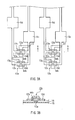
- FIG. 3A is a plan view showing an exemplary configuration of the bidirectional diodes 12 in the connection terminal region K, each of which connects the signal terminals 5 to each other.
- FIG. 3B is a cross-sectional view along the line A-A shown in FIG. 3A .
- two diodes 12a with opposite directions are connected to each other in parallel between two lines extending from electrodes forming the signal terminals 5.
- One of the two diodes 12a is formed by a transistor whose gate and drain are connected to each other and the other diode is formed by a transistor whose gate and source are connected to each other.
- a source electrode 12s extends inwardly from one of the lines and a drain electrode 12d extends inwardly from the other line, and they oppose each other around midway between the two lines.
- the gate electrode 12g is provided such that it runs below the area between the tip of the source electrode 12s and the tip of the drain electrode 12d, and partially overlaps with the tip of the source electrode 12s and the tip of the gate electrode 12g.
- An insulating layer 16 is provided on the gate electrode 12g such that the gate electrode 12g is covered with the insulating layer 16.
- a semiconductor layer 12h is formed so as to overlap with the gate electrode 12g.
- the semiconductor layer 14h is formed in the area from the tip of the source electrode 12s to the tip of the drain electrode 12d.
- the area between the gate electrode 12g and the source electrode 12s is a source area
- the area between the gate electrode 12g and the drain electrode 12d is a drain area.
- the area between the source area and the drain area serves as a channel area.
- the gate electrode 12g is connected to one of the lines extending from the signal lines through, for example, a contact hole 17.
- the configuration of the diodes is not limited to the example shown in FIGS. 3A and 3B .
- a PN connection using P and N areas aligned in order can be used in place of a transistor connection.
- the diodes 12a, 12b shown in FIG. 3 are used, for example, to connect signal terminals to each other in order to test a break in the bus lines and the connection lines.
- elements such as current measuring transistors and lighting transistors are to be placed in the connection terminal region K, they need to have a certain size in order to reduce resistance and to ensure allowable current. In this case, the elements are expected to become larger in size than the diodes shown in FIG. 3 . The same goes for the case of using either a-Si or p-Si.
- connection terminal region K e.g., the IC mounting portion
- switching elements such as Tr
- the connection terminal region K e.g., the IC mounting portion
- the input ends of the lines inside the panel i.e., the bus lines such as the scanning lines 1 and the data lines 2 and the connection lines 3.
- the bus lines such as the scanning lines 1 and the data lines 2 and the connection lines 3.
- elements for display and current measuring purposes that have a certain level of resistance or allowable current or high mobility (polycrystal Si channel) are used, it will be difficult to secure the space for placing these elements. This is because, in recent years, COG IC chips are required to be small in size and to high definition compatible. Therefore, by placing between signal terminals the diode 12 for testing continuity, and controlling test signal inputs on a group basis through the test lines 8 and the transistors 4 as in the above embodiment, it is possible to reduce the size of the testing elements provided in the connection terminal region K.
- connection elements may take forms other than the modified examples described below. Further, the modified examples described below can also be applied to other embodiments described later.
- FIG. 4A is a diagram showing a modified example of the diodes 12.
- each unidirectional diode is provided between the signal terminals 5 in place of the bidirectional diodes.
- each signal terminal is connected to only one adjacent signal terminal through one bidirectional diode 12.
- the number of the connection elements e.g., diodes
- the number of the connection elements can be reduced, so that the space for placing the connection elements can be further reduced.
- every two signal terminals belonging to different groups here, the groups A and C as an example
- the signal terminals 5a and 5c are connected to each other through one bidirectional diode but signal terminals belonging to the same group may be connected to each other through one bidirectional diode.
- unidirectional diodes 12a can be used as connection elements in place of the bidirectional diodes. In this case, the space for placing the connection elements can be further reduced.
- one signal terminal is connected to both adjacent signal terminals through the bidirectional diodes 12. That is, two bidirectional diodes 12 for connecting signal terminals to each other are provided for every three signal terminals. According to this configuration, it is possible to check whether there is any break in lines by inputting signals to, of the three signal terminals (e.g., 5b 1 , 5d 1 , 5b 2 ), only the signal terminal sitting at the center (5d 1 ). Further, the three signal terminals connected to each other through the diodes 12 may include signal terminals belonging to different groups as shown in FIG. 4D . Alternatively, three signal terminals belonging to the same group may be connected to each other through the diodes.
- the unidirectional diodes 12a are provided such that a current flows from one signal terminal to both adjacent signal terminals.
- the unidirectional diodes 12a are provided such that a current flows to one signal terminal from both adjacent signal terminals. That is, the diodes 12a in FIG. 4F have an opposite polarity from that of the diodes 12a shown in FIG. 4E . In this way, by using the unidirectional diodes 12a, it is possible to restrict the voltage direction as well as to further reduce the space for placing the connection elements.
- transistors are used as connection elements in place of the diodes.
- the source electrode of each transistor is connected to one signal terminal and the drain electrode of each transistor is connected to the other signal terminal.
- the gate electrode is connected to, for example, a line over which a control signal for controlling the transistor to be turned on/off is transmitted.
- three signal terminals are connected to each other through one transistor 14.
- the gate electrode of the transistor is connected to the signal terminal 5d 1 sitting at the center, and the source electrode and the drain electrode of the transistor are respectively connected to the signal terminals 5b 1 , 5d 2 sitting on both sides of the signal terminal 5d 1 .
- the source electrode and the drain electrode of each transistor are respectively connected to two adjacent signal terminals, and the gate electrode of each transistor is connected to a signal terminal adjacent to the two transistors.
- the example shown in FIG. 4I is an example where the gate is not connected to the signal terminal sitting at the center.
- FIG. 5 is a plan view showing a schematic configuration of a liquid crystal panel 200 according to Embodiment 2.
- the same portions as in FIG. 1 are denoted by the same reference numerals.
- the signal terminals 5 in the connection terminal region K are connected to a short line 13 through the bidirectional diodes 12.
- the signal terminals 5a connected to the scanning lines 1a of the group A and the signal terminals 5c connected to the scanning lines 1c of the group C are connected, through the diodes 12, to one short line 13 connected to a test signal terminal 9ac.
- the signal terminals 5b connected to the scanning lines 1b of the group B and the signal terminals 5d connected to the scanning lines 1d of the group D are connected, through the diodes 12, to one short line 13 connected to a test signal terminal 9bd.
- the signal terminals 5e connected to the data lines 2e of the group E and the signal terminals 5f connected to the date lines 2f of the group F are connected, through the diodes 12, to one short line 13 connected to a test signal terminal 9ef.
- the active matrix substrate 101 includes the transistors 4 provided for inputting test signals to the bus lines (the scanning lines 1 and the data lines 2) in the pixel region P, the lines 7 for dividing the transistors 4 into groups to control the transistors 4 to be turned on/off on a group basis, and one or more short lines 13 placed in the connection terminal region K (in the vicinity of the input ends of the bus lines). And the bus lines are connected to the corresponding short lines 13 through the diodes 12. According to this configuration, it is possible to reduce the size of test elements in the connection terminal region K and to test not only the lines inside the pixel region but also the lines outside the pixel region for breaks.
- FIG. 6 is a diagram showing a modified example of the connection elements.
- the unidirectional diodes 12a are used as the connection elements in place of the bidirectional diodes 12.
- unidirectional diodes whose direction is opposite to that of the unidirectional diodes 12a shown in FIG. 6 can also be used.
- connection terminal region K e.g., the IC mounting portion
- test signals to the data lines 2 are inputted from the additional signal terminals 11R, 11G, 11B. Furthermore, to the short line 13 connected to the scanning lines 1 through the diodes (i.e., to the test signal terminals 9ab, 9cd), test signals to the scanning lines are inputted.
- test signals are inputted to the data lines 2 of the groups E and F through the test lines 8R, 8G, 8B, and test signals are inputted to the scanning lines 1 of the groups A to D from the short line 13 through the signal terminals 5a to 5d and the connection lines 3a to 3b. All test signals to the scanning lines 1 are inputted through the diodes 12. It is desirable that the test signals inputted to the scanning lines 1 at this time are at a low frequency (or a DC potential).
- test signals are inputted to the scanning lines 1 from the additional signal terminals 11a, 11b, 11c, 11d, and test signals are inputted to the data lines 2 from the short line 13 to which the signal terminals 5e, 5f (test signal terminal 9ef) are connected.
- test signals are inputted to the data lines 2 of the groups E and F from the short line 13 through the signal terminals 5e, 5f and the connection lines 3e, 3f, and test signals are inputted to the scanning lines 1 of the groups A to D through the test lines 8a to 8b. All test signals to the data lines 2 are inputted through the diodes 12. As a result, it is possible to test the connection lines 3a to 3d in addition to the scanning lines 1 for breaks.
- the area of the connection terminal region K for the test elements becomes larger than that in Embodiment 1, but it is possible to reduce the number of sections to be checked and thus the number of man-hours.
- FIG. 7 is a plan view showing a schematic configuration of a liquid crystal panel 300 according to Embodiment 3.
- each signal terminal 5 in the connection terminal region K is connected to only one adjacent signal terminal through a transistor 14.
- the source electrode and the drain electrode of each transistor 14 are connected to the signal terminals, and the gate electrode of each transistor is connected to one short line 13.
- Each signal terminal 5 is connected to one short line 13 through the transistor 14.
- the signal terminals 5a connected to the scanning lines 1a of the group A and the signal terminals 5c connected to the scanning lines 1c of the group C are connected, through the transistors 14, to one short line 13 connected to the test signal terminal 9ac. That is, each signal terminal is connected to only one adjacent signal terminal through the transistor 14.
- the drain electrodes of the transistors 14 are connected to the signal terminals 5a of the group A, the source electrodes of the transistors 14 are connected to the signal terminals 5c of the group C, and the gate electrodes of the transistors 14 are connected to the short line 13.
- every two signal terminals of the signal terminals 5 aligned are connected to each other through one transistor 14.
- the signal terminals 5b connected to the scanning lines 1b of the group B and the signal terminals 5d connected to the scanning lines 1d of the group D are connected, through the transistors 14, to one short line 13 connected to the test signal terminal 9bd.
- the signal terminals 5e connected to the data lines 2e of the group E and the signal terminals 5f connected to the data lines 2f of the group F are connected, through the transistors 14, to one short line 13 connected to the test signal terminal 9ef.
- the signal terminals connected to the bus lines belonging to different groups are connected to each other through a transistor. That is, the groups A and C are connected to each other, the groups B and D are connected to each other, and the groups E and F are connected to each other through the transistors 14 in the connection terminal region K.
- the active matrix substrate 101 includes the transistors 4 provided for inputting test signals to the bus lines (the scanning lines 1 and the data lines 2) in the pixel region P, the lines 7 for dividing the transistors 4 into groups to control the transistors 4 to be turned on/off on a group basis, and the transistors 14 each of which is provided to connect every two lines in the connection terminal region K (in the vicinity of the input ends of the bus lines) to each other. According to this configuration, it is possible to reduce the size of the test elements in the connection terminal region K and to test not only the lines inside the pixel region but also the lines outside the pixel region for breaks.
- connection terminal region K e.g., the IC mounting portion
- the transistors 4c 1 , 4c 2 of the group C and the transistors 4d 1 , 4d 2 of the group D are turned off, and the transistors of the remaining groups (A, B, E, F), i.e., the transistors 4a, 4b, 4e, 4f, are turned on.
- test signals are inputted from the additional signal terminals 11a, 11b. It is desirable that the test signals inputted to the scanning lines at this time are at a low frequency (or a DC potential). Further, test signals are inputted also to the data lines 2e, 2f, from the additional signal terminals 11R, 11G, 11B.
- the test signals are inputted to the scanning lines 1a of the group A through the transistors 4a and are inputted to the scanning lines 1b of the group B through the transistors 4b. Further, the test signals that have been inputted to the groups A and B are inputted to the scanning lines 1c of the group C and the scanning lines 1d of the group D (and d) through the transistors 14 in the connection element region K. That is, the test signals that have been inputted to the scanning lines through the transistors 4a, 4b pass through the connection lines 3a, 3b and reach the signal terminals 5b. Then, they enter the connection lines 3c, 3b from the adjacent signal terminals 5c, 5d through the transistors 14, and are inputted to the scanning lines 1c, 1d.
- connection line 3d 1 between the scanning line 1d 1 and the signal terminal 5d 1 as shown in FIG. 7 .
- no test signal will be inputted to the scanning line 1d 1 .
- the pixels of the group d corresponding to the scanning line 1d 1 do not get turned on. Consequently, the break in the connection line 1d 1 can be detected.
- Embodiment 3 it is possible to further reduce the element area in comparison with Embodiments 1 and 2. Further, it is possible to reduce the number of sections to be checked in comparison with Embodiment 1.
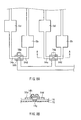
- FIG. 8A is a plan view showing an exemplary configuration of the transistors 14 in the connection terminal region K shown in FIG. 7 .
- FIG. 8B is a cross-sectional view along the line A-A shown in FIG. 8A .
- a source electrode 14s extends inwardly from one of the lines and a drain electrode 14d extends inwardly from the other line, and they oppose each other around midway between the two lines.
- the gate electrode 14g is provided such that it runs below the area between the tip of the source electrode 14s and the tip of the drain electrode 14d, and partially overlaps with the tip of the source electrode 14s and the tip of the gate electrode 14g.
- An insulating layer 16 is provided on the gate electrode 14g such that the gate electrode 14g is covered with the insulating layer 16.
- a semiconductor layer 14h is formed so as to overlap with the gate electrode 14g.
- the semiconductor layer 14h is formed in the area from the tip of the source electrode 14s to the tip of the drain electrode 14d.
- the area between the gate electrode 14g and the source electrode 14s is a source area
- the area between the gate electrode 14g and the drain electrode 14d is a drain area.
- the area between the source area and the drain area serves as a channel area.
- a shielding film 15 for shielding the transistors 4 from external light is provided between the gate electrode 14g and the substrate (not shown).
- the shielding film 15 may be provided in the entire connection terminal region K or only at the portions where the transistors 14 are formed. It is preferable that the shielding film 15 is made of a material that is less reflective and less translucent. For example, it is preferable to use an organic film having a high OD (Optical Density) value to form the shielding film 15, but the material of the shielding film 15 is not particularly limited.
- the configuration of the transistors is not limited to the example shown in FIGS. 8A and 8B .
- the transistors may be configured such that the positional relationship between the gate electrode and the source and drain electrodes is upside down (a so-called top gate type).
- the transistors forming the diodes as shown FIGS. 3A and 3B also may be of a top gate type.
- FIG. 9 is a diagram showing a modified example of the connection elements in the connection terminal region K.
- each signal terminal 5 is connected to one adjacent signal terminal through one transistor 14.
- the source electrode and the drain electrode of each transistor 14 are connected to the signal terminals through the diodes 12, and the gate electrode of each transistor 14 is connected to the short lines 13.
- the direction of the diode 12 connected to the source electrode and the direction of the diode 12 connected to the drain electrode are set such that a current flows from the source electrode to the drain electrode or from the drain electrode to the source electrode.
- the direction of the diodes 12 is set such that a current flows from the signal terminal 5a of the group A to the signal terminal 5c of the group C.
- the configuration shown in FIG. 9 it is possible to control signal terminal connections between given groups through the transistors 14 and the diodes 12.
- the configuration shown in FIG. 9 is merely an example, the configuration of combination of the transistors 14 and the diodes 12 is not limited to this example.
- the step of severing the connection elements in the connection terminal region K, such as the diodes 12 and the transistors 14, may be performed after the testing step.
- the step of electrically separating the diodes 12 and the transistors 14 shown in FIGS. 1 , 4 and 7 from the signal terminals 5 may be included.
- lines between the signal terminals 5 and the diodes 12 or the transistors 14 may be severed.
- the lines may be severed with a laser.
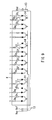
- FIG. 10A is a diagram showing a circuit configuration in the connection terminal region K shown in FIG. 1 after the severance of the lines between the signal terminals 5 and the diodes 12 as the connection elements.
- the lines are severed along a dotted line C 1 as a severing line running between the signal terminals 5 and the diodes 12.
- the severing line is not limited to C 1 , and C 2 can be used as severing lines.
- FIG. 10B is a diagram showing a circuit configuration in the connection terminal region K shown in FIG. 5 after the severance of the lines between the signal terminals 5 and the diodes 12 as the connection elements.
- the lines are severed along a dotted line C 3 as a severing line running between the signal terminals 5 and the diodes 12.
- the portions to be severed are not limited to those in the examples shown in FIGS. 10A and 10B .
- at least a part of lines between the connection elements, lines connected to the connection elements, and lines around connection the elements can be severed.
- the scanning lines 1 are divided into the groups A to D, and the data lines 2 are divided into the groups E and F, and control lines for controlling the transistors 4 on a group basis are provided. That is, the scanning lines 1 and the data lines 2 are both divided into a plurality of groups but the groupings are not limited to this.
- one of the scanning lines 1 and the data lines 2 can be grouped together and the other can be to divide into a plurality of groups.
- the scanning lines 1 can be grouped together.
- control lines 7a to 7f for turning the transistors 4 on/off are provided for the groups A to F, respectively, but it is possible to connect the gate electrodes of the transistors 4 of different groups collectively to one control line. That is, the gate electrodes of the switching elements that belong to different groups may be connected to a common control line.
- the transistors 4a, 4c are respectively connected to the scanning lines of the groups A and C, the groups of the scanning lines drawn to the left side of the pixel region P, and the gate electrodes of the transistors 4a and the gate electrodes of the transistors 4c are connected to the control lines 7a, 7c, respectively.
- control line 7a for the transistors 4a and the control line 7c for the transistors 4c can be brought together into one line. In this way, by collectively shearing a control line among different groups, the number of lines can be reduced, thereby facilitating a reduction in the frame area.
- input signals can be controlled on a group basis by providing additional connection lines for each group.
- the additional connection lines 8a to 8d are provided for the groups A to D, respectively, but it is possible to connect the scanning lines of different groups collectively to one additional connection line.
- the additional connection lines 8a, 8c that are connected to the scanning lines of the respective groups A and C, the groups of the scanning lines drawn to the left side of the pixel region P can be brought together into one line.
- the number of lines can be reduced, thereby faciliating a reduction in the frame area.
- input signals can be controlled on a group basis by, for example, providing additional connection lines for each group.
- paths through which signals are inputted to the bus lines from the additional signal terminals through the additional connection lines may be collectively sheared among different groups or may be provided for each group.
- control lines for the switching elements for controlling connections between the additional connection lines and the bus lines may be collectively shared among different groups or may be provided for each group. In this way, it is possible to correspond the additional connection lines and the control lines with each groups as needed.
- FIG. 11 is a diagram showing a modified example of the switching elements and the lines.
- the scanning lines 1a, 1c, (the groups A, C) drawn to the right side of the pixel region P are both connected to a common additional connection line 8ac.
- the scanning lines 1b, 1d, (the groups B, D) drawn to the left side of the pixel region P are both connected to a common additional connection line 8bd.
- the gate electrodes of the transistors 4e, 4f are connected to a common control line 7.
- the operations during the test in the example shown in FIG. 11 can be performed in the same manner as in Embodiment 1.
- the liquid crystal panels according to Embodiments 1 to 3 can be used in electronic devices for portable terminal uses, such as mobile phones, PDAs (Personal Digital Assistants), PHS (Personal Handy-phone System) devices, and HHTs (hand held terminals).
- electronic devices for portable terminal uses such as mobile phones, PDAs (Personal Digital Assistants), PHS (Personal Handy-phone System) devices, and HHTs (hand held terminals).
- the liquid crystal panels can also be used in such electronic devices as game terminals, car navigation systems, personal computers, television sets, video cameras, and digital cameras.
- the application of the active matrix substrate 101 according to each of Embodiments 1 to 3 is not limited to a liquid crystal panel.
- the active matrix substrate 101 can also be used in such panels (display devices) as field emission displays, plasma displays, and organic EL displays.
- Embodiments 1 to 3 It is possible to form a liquid crystal display device by further providing the liquid crystal panel according to each of Embodiments 1 to 3 with a light source unit and a driver IC or an FPC connected to a driver.
- the present invention is useful as an active matrix substrate, a display device, a method for testing the active matrix substrate, and a method for testing the display device.
Landscapes
- Engineering & Computer Science (AREA)
- Physics & Mathematics (AREA)
- General Physics & Mathematics (AREA)
- Theoretical Computer Science (AREA)
- Computer Hardware Design (AREA)
- Chemical & Material Sciences (AREA)
- Crystallography & Structural Chemistry (AREA)
- Nonlinear Science (AREA)
- Liquid Crystal (AREA)
- Optics & Photonics (AREA)
- Mathematical Physics (AREA)
- Microelectronics & Electronic Packaging (AREA)
- Devices For Indicating Variable Information By Combining Individual Elements (AREA)
- Liquid Crystal Display Device Control (AREA)
- Control Of Indicators Other Than Cathode Ray Tubes (AREA)
Abstract
Description
- The present invention relates to an active matrix substrate having a pixel region provided with a plurality of bus lines, a display device, a method for testing the active matrix substrate, and a method for testing the display device.
- As a way to test the drive of a display panel that includes an active matrix pixel region (e.g., a liquid crystal display panel), it is known to provide the display panel with elements for inputting test signals to the pixel region to turn on the pixels. For example, it has been disclosed that thin film transistors (TFTs) are provided between every adjacent gate lines in the pixel region to switch continuity between the adjacent gate lines from on to off, and vice versa (see
Patent Document 1, for example). In this configuration, the value of a current that flows through two gate lines brought into conduction by the TFTs is measured. - The configuration described above requires a current input source and space for inserting all of the between-gate line transistors. Moreover, in order to carry out a current measurement, it is necessary to take the resistance and the current tolerance of the transistors into consideration. However, to increase the size of the pixel region in which images are displayed, it is necessary to reduce the size of the periphery of the pixel region. Therefore, it is difficult to secure space for placing the TFTs and the lines used for testing. For these reasons, it has been proposed to place terminals in the area for placing semiconductor chips (see Patent Documents 2 and 3, for example).
-
- Patent Document 1:
JP 2001-147650 A - Patent Document 2:
JP 2004-101863 A - Patent Document 3:
JP 2007-171993 A - However, the semiconductor chips for driving liquid crystal are also preferably small in size. In the conventional technique described above, since the terminals and elements used for testing also require a certain size of space, it is difficult to place them in the semiconductor chip mounting area. Thus, when adding components for inputting signals to the pixel region, such as elements for testing, the signal input means to be added need to be small in size.
- With the foregoing in mind, it is an object of the present invention to facilitate a reduction in the size of elements that are added for inputting signals.
- The active matrix substrate disclosed in the present application includes: a plurality of bus lines provided in a pixel region; a plurality of signal terminals for inputting a driving signal to each of the bus lines, the signal terminals being provided in a connection terminal region situated outside the pixel region; connection lines for connecting the signal terminals to the bus lines; additional signal terminals for inputting a signal to the bus lines through different paths from those used in inputting the driving signal from the signal terminals, the additional signal terminals being provided outside the pixel region; additional connection lines for connecting the bus lines to the additional signal terminals; and a plurality of switching elements for controlling connections between the bus lines and the additional connection lines. The switching elements are divided into a plurality of groups, and can control connections between the bus lines and the additional connection lines on a group basis, and connection elements that each comprise a diode or a switching element and connect the signal terminals to each other are provided in the connection terminal region.
- In the above configuration, the switching elements for inputting signals to each of the bus lines through different paths from those used in inputting driving signals from the signal terminals are controlled on a group basis. Further, the signal terminals for inputting driving signals to each of the bus lines through the connection lines are connected to each other through the connection elements. Therefore, if the switching elements of a given group are turned on and signals are inputted from the additional signal terminals to the bus lines of the given group, the signals will also reach the signal terminals from the bus lines through the connection lines, and be inputted to other connection lines and bus lines that are connected to each other through the connection elements. As a result, it is possible to test not only the bus lines provided in the pixel region but also the connection lines that connect the bus lines to the signal terminals for continuity. Further, since the connection elements each include a diode or a switching element, and they can be used specifically for checking continuity (breaks) of the bus lines and the connection lines, it is possible to reduce the size of the elements. Consequently, it is possible to place the elements in a downsized or minuscule semiconductor chip mounting portion, an FPC portion or the surroundings thereof.
- In the above configuration, the bus lines are lines for sending signals to pixels arranged in the pixel region in a matrix. The bus lines may include a plurality of scanning signal lines for sending scanning signals to pixels in each column and a plurality of video signal lines arranged perpendicular to the scanning signal lines for sending video signals to pixels in each row.
- The switching elements are divided into a plurality of groups, and are controlled to be turned on/off on a group basis. For example, by connecting control signal input terminals for the switching elements belonging to the same group to one line, the switching elements can be controlled on a group basis. That is, a control line used for controlling the switching elements to be turned on/off can be provided for each group. For example, groupings can be made based on the gate lines and the source lines, odd-numbered columns (rows) and even-numbered columns (rows), RGB, and blocks.
- The connection terminal region is a region provided outside the pixel region and in which the signal terminals for connecting the bus lines to the outside of the substrate are placed. For example, in a model that was produced by a so-called COG (Chip On Glass) method, a method of directly mounting an IC on an active matrix substrate, the IC mounting portion can be defined as the connection terminal region. Alternatively, a flexible printed circuit (FPC) may be connected to the connection terminal region. Further, the connection terminal region may be provided around the IC or FPC mounting portion.
- It is preferable that the connection elements are each provided between the signal terminals connected to the bus lines belonging to different groups.
- By connecting to each other through the connection elements the signal terminals connected to the bus lines belonging to different groups, it is possible to input signals that have been inputted one group of bus lines to other group of bus lines through the connection lines.
- The connection elements may be bidirectional diodes, unidirectional diodes or transistors.
- If the signal terminals connected to the bus lines belonging to different groups are connected to each other through transistors, it is possible to cut the number of the elements into half, so that the space can be reduced. Especially, when the connection terminal region serves as an IC mounting portion where an IC is mounted, this spacing-saving effect becomes more significant due to the trends toward reductions in size of ICs. Further, when different groups are connected to each other through diodes, the diodes can serve as an anti-static pattern.
- Each of the signal terminals may be configured to be connected to only one adjacent signal terminal through the connection element.
- As a result, it is possible to provide one connection element for every two signals terminals of the signal terminals provided in a row. As a result, it is possible to reduce the number of the elements in the connection terminal region, so that further spacing-saving can be achieved.
- The active matrix substrate may be configured to further include a short line that connects the signal terminals and an additional signal terminal for inputting a signal for turning pixels on, and the connection elements are provided between the signal terminals and the short line.
- As a result, the signal terminals are connected to each other through the short line and the connection elements. Thus, test signals inputted from the additional signal terminal can be inputted to the bus lines through the short line and the signal terminals.
- The active matrix substrate may be configured to include a plurality of short lines that connect a plurality of sets of the signal terminals and a plurality of additional terminals, respectively, the connection elements are provided between the signal terminal of the respective sets and each short line, and each of the sets includes the signal terminals connected to the switching elements belonging to at least one of the groups.
- As a result, it is possible to input signals for turning on pixels collectively from the short lines to sets of signal terminals corresponding to the groups of bus lines. For example, signals may be inputted to all of the short lines at once or signal may be inputted from the additional signal terminals of the short lines based on the same or different groups from the groups of bus lines as needed.
- The connection elements may be transistors that control connections between the signal terminals, and a gate electrode and a source electrode of each transistor may be connected to two signal terminals and a source electrode of each transistor may be connected to the short line.
- As a result, it is possible to control connections between the signal terminals through the short lines.
- The active matrix substrate may further include a shielding film for shielding the connection elements from external light. The shielding film can suppress external light's influence on the connection elements.
- One connection element may be provided for every three continuous signal terminals, and connect the signal terminal at the center of the three signal terminals to the signal terminals on both sides. Consequently, by inputting signals to the signal terminal situated at the center, the signals can be also transmitted to the lines connected to the three signal terminals.
- A display device including the above-described active matrix substrate is also one embodiment of the present invention.
- The test method disclosed in the present application is a method for testing an active matrix substrate. The active matrix substrate includes: a plurality of bus lines provided in a pixel region; a plurality of signal terminals for inputting a driving signal to each of the bus lines, the signal terminals being provided in a connection terminal region situated outside the pixel region; connection lines for connecting the signal terminals to the bus lines; connection elements for connecting the signal terminals to each other in the connection terminal region; additional signal terminals for inputting a signal to each of the bus lines through different paths from those used in inputting the driving signal from the signal terminals, the additional signal terminals being provided outside the pixel region; additional connection lines for connecting the bus lines to the additional signal terminals; and a plurality of switching elements for controlling connections between the bus lines and the additional connection lines, the switching elements being divided into two or more groups. The method includes the steps of: turning on connections between the additional connection lines and the bus lines belonging to at least one of the groups; and inputting signals from the additional signal terminals. The inputted signals are inputted to the bus lines through the switching elements turned on and reach the signal terminals through the connection lines, and are further inputted to other connection lines and bus lines from other signal terminals through the connection elements.
- The test method disclosed in the present application is a method for testing an active matrix substrate. The active matrix substrate includes: a plurality of bus lines provided in a pixel region; a plurality of signal terminals for inputting a driving signal to each of the bus lines, the signal terminals being provided in a connection terminal region situated outside the pixel region; connection lines for connecting the signal terminals to the bus lines; a short line connected to the signal terminals; connection elements provided between the signal terminals and the short line; additional signal terminals for inputting a signal to each of the bus lines through different paths from those used in inputting the driving signal from the signal terminals, the additional signal terminals being provided outside the pixel region; additional connection lines for connecting the bus lines to the additional signal terminals; and a plurality of switching elements for controlling connections between the bus lines and the additional connection lines, the switching elements being divided into two or more groups. The method includes the steps of: turning on connections between the additional connection lines and the bus lines belonging to at least one of the groups; inputting signals from the additional signal terminals; allowing the inputted signal to be inputted to the bus lines through the switching elements turned on; and inputting, through the short line and the connection elements, signals for turning on pixels of the bus lines to which the inputted signals have been inputted.
- The above test methods may further include the step of severing at least a part of the connection elements after testing the pixels using the signals for turning on pixels.
- According to the active matrix substrate disclosed in the present application, it is possible to facilitate a reduction in the size of elements that are formed on the outside of the panel display portion.
-
- [
FIG. 1] FIG. 1 is a plan view showing a schematic configuration of a liquid crystal panel according toEmbodiment 1. - [
FIG. 2] FIG. 2 is a diagram for explaining one example of a method for testing pixels of the liquid crystal panel shown inFIG. 1 . - [
FIG. 3] FIG. 3A is a plan view showing an exemplary configuration of bidirectional diodes, each of which connects signal terminals in a connection terminal region K to each other.FIG. 3B is a cross-sectional view along the line A-A shown inFIG. 3A . - [
FIG. 4] FIGS. 4A to 4I are diagrams showing modified examples of connection elements. - [
FIG. 5] FIG. 5 is a plan view showing a schematic configuration of a liquid crystal panel according to Embodiment 2. - [
FIG. 6] FIG. 6 is a diagram showing a modified example of connection elements. - [
FIG. 7] FIG. 7 is a plan view showing a schematic configuration of a liquid crystal panel according to Embodiment 3. - [
FIG. 8] FIG. 8A is a plan view showing an exemplary configuration of transistors in the connection terminal region K shown inFIG. 7 .FIG. 8B is a cross-sectional view along the line A-A shown inFIG. 8A . - [
FIG. 9] FIG. 9 is a diagram showing a modified example of connection elements in the connection terminal region. - [
FIG. 10 ]FIG. 10A is a diagram showing a circuit configuration after the severance of the lines between the connection elements and the signal terminals in the connection terminal region.FIG. 10B is a diagram showing a modified example of the severing line. - [
FIG. 11] FIG. 11 is a diagram showing one modified example of the switching elements and the lines. - Hereinafter, more specific embodiments of the present invention will be described with reference to the drawings. The following embodiments show exemplary configurations of the display device of the present invention being embodied in the form of a liquid crystal display device.
- For convenience of explanation, each of the drawings that is to be referred to in the following schematically shows only the main members required to describe the present invention, among the constituent members of the embodiments of the present invention. Therefore, the display device of the present invention may include any constituent members that are not shown in the following drawings that are referred to herein. The size of and size ratio of the constituent members in the following drawings do not exactly reflect those of the actual constituent members.
- Hereinafter, preferred embodiments of the active matrix substrate and the display device of the present invention will be described with reference to the drawings. In the following description, the present invention is applied to a transmission-type liquid crystal display device as an example.
-
FIG. 1 is a plan view showing a schematic configuration of aliquid crystal panel 100 according toEmbodiment 1. As shown inFIG. 1 , theliquid crystal panel 100 includes anactive matrix substrate 101 and acounter substrate 102 opposing theactive matrix substrate 101. A liquid crystal material (not shown) is sandwiched between theactive matrix substrate 101 and thecounter substrate 102. In order to show the layout of lines and electrodes on theactive matrix substrate 101, thecounter substrate 102 and the liquid crystal layer are shown in perspective view inFIG. 1 . - The
counter substrate 102 used in the present embodiment includes a color filter layer having R (red), G (green), and B (blue) color filters and a black matrix for preventing leakage of light from the color filters. A common electrode is formed on the color filter layer. - It should be noted that the above counter substrate is merely an example, and the scope of the counter substrate includes counter substrates of various specifications, for example, a substrate including color filters containing color materials of more than three colors or color materials whose colors are completely different from the three primary colors, a transparent or semi-transparent substrate containing no color material, a substrate including no common electrode, a substrate including only a shielding layer, a substrate having a touch input function, and a mere substrate without any of the structures mentioned.
- The
active matrix substrate 101 includes a pixel region P, a connection terminal region K, and a frame-shaped wiring region SR situated outside the pixel region P and surrounding the pixel region P. Further, pixel electrodes, thin film transistors (TFTs), and the like are formed between theactive matrix substrate 101 and the liquid crystal layer in relation to a plurality of pixels included in the pixel region P (display surface) of theliquid crystal panel 100. - In the following, one of the sides of the
liquid crystal panel 100 close to the connection terminal region K will be referred to as a first side S1 (the lower side inFIG. 1 ), the left and the right sides opposing each other through the first side S1 will be referred to as a second side S2 and a third side S3, respectively, and the side opposing the first side S1 will be referred to as a fourth side S4. - Here, as shown in
FIG. 1 , the second side S2 (the third side S3) of theactive matrix substrate 101 is larger than the second side S2 (the third side S3) of thecounter substrate 102 in length. Thus, when theactive matrix substrate 101 and thecounter substrate 102 are put together through the liquid crystal material, the connection terminal region K of theactive matrix substrate 101 is situated close to the first side S1 and outside of thecounter substrate 102. - In the pixel region P, a plurality of
scanning lines scanning lines 1 as needed. The same goes for data lines 2, connection lines 3, transistors 4, signal terminals 5, and the like), and a plurality of data lines 2e1, 2f1, 2e2, 2f2, 2...2en, and 2fn orthogonal to thescanning lines 1 are formed. The scanning lines and the data lines can be referred to as gate lines and source lines, respectively. Further, the data lines are also referred to as signal lines in some cases. Note that thescanning lines 1 and the data lines 2 are examples of the bus lines. - On a transparent glass or transparent synthetic resin base (not shown) included in the
active matrix substrate 101, thescanning lines 1 and the data lines 2 are arranged in a matrix so as to cross each other. That is, the data lines 2 are arranged on the base so as to be parallel to the column-wise direction of the matrix (the vertical direction of the liquid crystal panel 2) and thescanning lines 1 are arranged on the base so as to be parallel to the row-wise direction of the matrix (the lateral direction of the liquid crystal panel 2). - Although not being shown, lines other than the scanning lines and the data lines may be provided in the pixel region P as needed. For example, auxiliary capacitance lines for generating auxiliary capacitance may be provided.
- A thin film transistor as a switching element and a pixel having a pixel electrode connected to the thin film transistor are provided in the vicinity of each intersection of the scanning and
data lines 1, 2. Further, in the pixel region P, a common electrode is formed so as to oppose the pixel electrode of each pixel through the liquid crystal layer. That is, in theactive matrix substrate 101, a thin film transistor, a pixel electrode and a common electrode are provided for each pixel. - Further, in the
active matrix substrate 101, each segment of the area that is divided into a matrix by thescanning lines 1 and the data lines 2 has a plurality of pixel regions including red (R), green (G) and blue (B) pixels. These R, G, and B pixels are arranged, for example, in this order in succession so as to be parallel to the respective data lines 2e1, 2f1,... 2en, and 2fn. Furthermore, these R, G and B pixels can each display a corresponding color through the color filter layer (not shown) provided on thecounter substrate 102. - The connection terminal region K of the
active matrix substrate 101 is a region where the signal terminals 5 for inputting driving signals to thescanning lines 1 and the data lines 2 are placed. For example, in the connection terminal region K, a driver (not shown) or a flexible printed circuit (not shown) provided with a driver is connected to the signal terminals 5. As a result, thescan lines 1 and the data line 2 are connected to the driver electrically. - Specifically, in the connection terminal region K, the
signal terminals scan lines Connection lines scanning lines signal terminals bidirectional diode 12. A bidirectional diode can be defined as a diode composed of two diodes of opposite polarities (the direction in which a current flows) being connected to each other in parallel. - The
signal terminals scanning lines 1 serve as terminals to which scanning signals are inputted from the driver. Further, the signal terminals 5e, 5f connected to the data lines 2 serve as terminals to which data signals are inputted from the driver. It is possible to connect the driver to the connection terminal region K by, for example, a COG (Chip On Glass) method. Further, it is possible to connect a flexible printed circuit provided with a driver to the connection terminal region K by, for example, a TCP (Tape Carrier Package) method. Herein, the connection method to be taken is not particularly limited. - In the example shown in
FIG. 1 , only one driver can be placed in the connection terminal region K, but this is not the only configuration that can be taken. For example, theactive matrix substrate 101 may be provided with two or more connection terminal regions K and include two or more drivers placed in the respective connection terminal regions K. - Further, the driver placed in the connection terminal region K outputs scanning signals (gate signals) to the
scanning lines 1 one after another. Each scanning signal turns on the gate electrodes of the thin film transistors that correspond to the scanning line to which it is inputted. Further, the driver outputs to the data lines 2 data signals (voltage signal (gradation voltage) each corresponding to the brightness (gradation) of a displayed image. - In addition to the constituent members described above, the
active matrix substrate 101 includes additional signal terminals 11 for inputting signals to thescanning lines 1 and the data lines 2 through different paths from those used in inputting signals to thescanning lines 1 and the data lines 2 from the signal terminals 5. To the additional signal terminals 11, signals for testing whether pixels get turned on or not (hereinafter simply referred to as test signals) are inputted. Hereinafter, a case where test signals are inputted to the additional signal terminals 11 will be explained. It should be noted that this is not the only use of the additional signal terminals 11. - Further, in the frame-shaped wiring region SR, additional connection lines 8 for connecting the additional signal terminals 11 to the
scanning lines 1 and to the data lines 2 are formed, and transistors 4 (one example of the switching elements) for controlling connections between the additional connection lines 8 and thescanning lines 1 and connections between the additional connection lines 8 and the data lines 2 are further provided. - The transistors 4 are for switching from on to off and vice versa signal inputs from the additional signal terminals 11 to the
scanning lines 1 and the data lines 2. The transistors 4 are divided into a plurality of groups, and can control signal inputs to be enabled/disabled on a group basis. In the present embodiment, a control line for inputting control signals to the transistors 4 and a control signal terminal 9 connected to the control line are provided for each group. - For example, in the example shown in
FIG. 1 , odd-numbered (1st, 3rd, 5th...) scanning lines 1a, 1c of thescanning lines 1 are connected to theadditional connection lines transistors 4a, 4c provided on the left side (close to the side S2) of the frame-shaped wiring region SR. Thetransistors 4a, 4c on the left side are further divided into two groups (A, C). Thetransistors 4a are connected to thecontrol line 7a and thecontrol signal terminal 9a, and the transistors 4c are connected to thecontrol line 7c and thecontrol signal terminal 9c, independently on a group basis. That is, the gate electrodes of thetransistors control line 7a and thecontrol signal terminal 9a of the group A, and the gate electrodes of the transistors 4c1, 4c2 of the group C are connected to thecontrol line 7c and thecontrol signal terminal 9c of the group C. As a result, the groups A and C can control test signal inputs to be enabled/disabled independently. - Even-numbered (2nd, 4th, 6th...)
scanning lines scanning lines 1 are connected to theadditional connection lines transistors transistors transistors 4b are connected to thecontrol line 7b and thecontrol signal terminal 9b, and thetransistors 4d are connected to thecontrol line 7d and thecontrol signal terminal 9d, independently on a group basis. That is, the gate electrodes of thetransistors control line 7b and thecontrol signal terminal 9b of the group B, and the gate electrodes of thetransistors control line 7d and thecontrol signal terminal 9d of the group D. As a result, the groups B and D can control test signal inputs to be enabled/disabled independently. - The data lines 2 are connected to the
additional connection lines transistors transistors transistors 4e are connected to thecontrol line 7e and thecontrol signal terminal 9e and thetransistors 4f are connected to thecontrol line 7f and thecontrol signal terminal 9f, independently on a group basis. That is, the gate electrodes of thetransistors control line 7e and thecontrol signal terminal 9e of the group E, and the gate electrodes of thetransistors control line 7f and thecontrol signal terminal 9f of the group F. As a result, the groups E and F can control test signal inputs to be enabled/disabled independently. - Note that the groupings are not limited to the example described above. For example, the transistors for the data lines 2 can be divided into a group of transistors that are connected to data lines for R (red) gradation data, a group of transistors that are connected to data lines for G (green) gradation data, and a group of transistors that are connected to data lines for B (blue) gradation data.
-
FIG. 2 is a diagram for explaining one example of a test on pixels of theliquid crystal panel 100. Hereinafter, one example of a method for checking whether there is any break in each of the bus lines (thescanning lines 1 and the data lines 2) from the connection terminal region K to the pixel region P will be explained with reference toFIG. 2 . - First, of the transistors 4 for switching from on to off and vice versa connections between the
scanning lines 1 and the additional connection lines 8, the transistors 4c1, 4c2 of the group C and thetransistors transistors additional signal terminals additional signal terminals - As a result, the test signals are inputted to the scanning lines 1a of the group A through the
transistors 4a and the test signals are inputted to thescanning lines 1b of the group B through thetransistors 4b. Further, the test signals that have been inputted to the groups A and B are inputted to the scanning lines 1c of the group C and thescanning lines 1d of the group D (and d) through thediodes 12 in the connection element region K. That is, the test signals that have been inputted to the scanning lines through thetransistors signal terminals 5b. Then, they enter theconnection lines 3c, 3b from theadjacent signal terminals 5c, 5d through thediodes 12, and are inputted to thescanning lines 1c, 1d. Here, if there is a break in theconnection line 3d1 as shown inFIG. 2 , no test signal will be inputted to thescanning line 1d1. As a result, the pixels of the group d corresponding to thescanning line 1d1 do not get turned on. Consequently, the break in theconnection line 3d1 can be detected. - When inputting test signals to the bus lines of a given group, by disabling inputs from the test lines for the bus lines of other groups that are connected to each other through the signal terminal-connecting
diodes 12, it is possible to input the test signals to the other bus lines through thediodes 12 as in the above example. As described above, by connecting to each other the signal terminals of bus lines of different groups (e.g., between thesignal terminals 5a and 5c) through thebidirectional diodes 12, it is possible to test not only the bus lines (the scanning lines 1a to 1d) of the respective groups (e.g., the groups A to D) but also the connection lines (3a to 3d) that connect the respective groups to each other for breaks. - Note that the test method is not limited to the one described above. For example, by turning on the transistors of only one group, i.e., the
transistors transistors 4e of the group E), test signals can be inputted to the data lines 2e of the group E. In this case, the test signals are inputted to the data lines 2e of the group E from the test lines 8 through thetransistors 4e, and test signals are inputted to the data lines 2f of the group F through the connection lines and the signal terminals 5e, 5f. Therefore, it is possible to test not only the data lines 2e of the group E and the data lines 2f of the group F but also in the connection lines that connect the data lines 2e to the signal terminals 5e and the data lines 5f to the signal terminals 5f for breaks. - In the test method described above, the
diodes 12, each of which is provided between signal terminals in the connection terminal region K, are used to clarify differences in display state among pixels, which differences results from the presence or absence of breaks in the lines. In this way, by configuring thediodes 12 in the connection terminal region K to be used specifically for checking a break in the bus lines and the connection lines, thediodes 12 can be reduced in size. Further, thediodes 12 can also serve as an antistatic pattern. -
FIG. 3A is a plan view showing an exemplary configuration of thebidirectional diodes 12 in the connection terminal region K, each of which connects the signal terminals 5 to each other.FIG. 3B is a cross-sectional view along the line A-A shown inFIG. 3A . - In the example shown in
FIGS. 3A and 3B , twodiodes 12a with opposite directions are connected to each other in parallel between two lines extending from electrodes forming the signal terminals 5. One of the twodiodes 12a is formed by a transistor whose gate and drain are connected to each other and the other diode is formed by a transistor whose gate and source are connected to each other. - Specifically, between lines extending from electrodes forming the
signal terminals source electrode 12s extends inwardly from one of the lines and adrain electrode 12d extends inwardly from the other line, and they oppose each other around midway between the two lines. Thegate electrode 12g is provided such that it runs below the area between the tip of thesource electrode 12s and the tip of thedrain electrode 12d, and partially overlaps with the tip of thesource electrode 12s and the tip of thegate electrode 12g. An insulatinglayer 16 is provided on thegate electrode 12g such that thegate electrode 12g is covered with the insulatinglayer 16. And on the insulatinglayer 16, a semiconductor layer 12h is formed so as to overlap with thegate electrode 12g. Thesemiconductor layer 14h is formed in the area from the tip of thesource electrode 12s to the tip of thedrain electrode 12d. Of thesemiconductor layer 14h, the area between thegate electrode 12g and thesource electrode 12s is a source area, and the area between thegate electrode 12g and thedrain electrode 12d is a drain area. Of thesemiconductor layer 14h, the area between the source area and the drain area serves as a channel area. Thegate electrode 12g is connected to one of the lines extending from the signal lines through, for example, acontact hole 17. - Note that the configuration of the diodes is not limited to the example shown in
FIGS. 3A and 3B . For example, a PN connection using P and N areas aligned in order can be used in place of a transistor connection. - The
diodes 12a, 12b shown inFIG. 3 are used, for example, to connect signal terminals to each other in order to test a break in the bus lines and the connection lines. In contrast, if elements such as current measuring transistors and lighting transistors are to be placed in the connection terminal region K, they need to have a certain size in order to reduce resistance and to ensure allowable current. In this case, the elements are expected to become larger in size than the diodes shown inFIG. 3 . The same goes for the case of using either a-Si or p-Si. - Further, for a testing purpose, it may be considered to take an approach of providing switching elements, such as Tr, in the connection terminal region K (e.g., the IC mounting portion), the input ends of the lines inside the panel, i.e., the bus lines such as the
scanning lines 1 and the data lines 2 and the connection lines 3. In this case, if elements for display and current measuring purposes that have a certain level of resistance or allowable current or high mobility (polycrystal Si channel) are used, it will be difficult to secure the space for placing these elements. This is because, in recent years, COG IC chips are required to be small in size and to high definition compatible. Therefore, by placing between signal terminals thediode 12 for testing continuity, and controlling test signal inputs on a group basis through the test lines 8 and the transistors 4 as in the above embodiment, it is possible to reduce the size of the testing elements provided in the connection terminal region K. - Here, modified examples of the connection elements will be described. Note that the connection elements may take forms other than the modified examples described below. Further, the modified examples described below can also be applied to other embodiments described later.
-
FIG. 4A is a diagram showing a modified example of thediodes 12. In the example shown inFIG. 4A , each unidirectional diode is provided between the signal terminals 5 in place of the bidirectional diodes. Even with the configuration shown inFIG. 4 , it is possible to test a break in lines as in the above-described operations. In this way, by using unidirectional diodes as the connection elements, the space for placing the connection elements can be further reduced. - In the example shown in
FIG. 4B , each signal terminal is connected to only one adjacent signal terminal through onebidirectional diode 12. In this way, it is possible to provide one bidirectional diode for every two signal terminals of the signal terminals 5 provided in a row. According to this configuration, the number of the connection elements (e.g., diodes) can be reduced, so that the space for placing the connection elements can be further reduced. In the example shown inFIG. 4B , every two signal terminals belonging to different groups (here, the groups A and C as an example), i.e., thesignal terminals 5a and 5c, are connected to each other through one bidirectional diode but signal terminals belonging to the same group may be connected to each other through one bidirectional diode. - Furthermore, as shown in
FIG. 4C ,unidirectional diodes 12a can be used as connection elements in place of the bidirectional diodes. In this case, the space for placing the connection elements can be further reduced. - In the example shown in
FIG. 4D , one signal terminal is connected to both adjacent signal terminals through thebidirectional diodes 12. That is, twobidirectional diodes 12 for connecting signal terminals to each other are provided for every three signal terminals. According to this configuration, it is possible to check whether there is any break in lines by inputting signals to, of the three signal terminals (e.g., 5b1, 5d1, 5b2), only the signal terminal sitting at the center (5d1). Further, the three signal terminals connected to each other through thediodes 12 may include signal terminals belonging to different groups as shown inFIG. 4D . Alternatively, three signal terminals belonging to the same group may be connected to each other through the diodes. - In the example shown in
FIG. 4E , theunidirectional diodes 12a are provided such that a current flows from one signal terminal to both adjacent signal terminals. In the example shown inFIG. 4F , theunidirectional diodes 12a are provided such that a current flows to one signal terminal from both adjacent signal terminals. That is, thediodes 12a inFIG. 4F have an opposite polarity from that of thediodes 12a shown inFIG. 4E . In this way, by using theunidirectional diodes 12a, it is possible to restrict the voltage direction as well as to further reduce the space for placing the connection elements. - In the example shown in
FIG. 4G , transistors are used as connection elements in place of the diodes. The source electrode of each transistor is connected to one signal terminal and the drain electrode of each transistor is connected to the other signal terminal. The gate electrode is connected to, for example, a line over which a control signal for controlling the transistor to be turned on/off is transmitted. - In the example shown in
FIG. 4H , three signal terminals are connected to each other through onetransistor 14. The gate electrode of the transistor is connected to thesignal terminal 5d1 sitting at the center, and the source electrode and the drain electrode of the transistor are respectively connected to thesignal terminals signal terminal 5d1. - In the example shown in
FIG. 4I , the source electrode and the drain electrode of each transistor are respectively connected to two adjacent signal terminals, and the gate electrode of each transistor is connected to a signal terminal adjacent to the two transistors. The example shown inFIG. 4I is an example where the gate is not connected to the signal terminal sitting at the center. -
FIG. 5 is a plan view showing a schematic configuration of a liquid crystal panel 200 according to Embodiment 2. InFIG. 5 , the same portions as inFIG. 1 are denoted by the same reference numerals. In the example shown inFIG. 5 , the signal terminals 5 in the connection terminal region K are connected to ashort line 13 through thebidirectional diodes 12. Specifically, thesignal terminals 5a connected to the scanning lines 1a of the group A and the signal terminals 5c connected to the scanning lines 1c of the group C are connected, through thediodes 12, to oneshort line 13 connected to a test signal terminal 9ac. Thesignal terminals 5b connected to thescanning lines 1b of the group B and thesignal terminals 5d connected to thescanning lines 1d of the group D are connected, through thediodes 12, to oneshort line 13 connected to a test signal terminal 9bd. The signal terminals 5e connected to the data lines 2e of the group E and the signal terminals 5f connected to the date lines 2f of the group F are connected, through thediodes 12, to oneshort line 13 connected to a test signal terminal 9ef. - That is, the
active matrix substrate 101 according to the present embodiment includes the transistors 4 provided for inputting test signals to the bus lines (thescanning lines 1 and the data lines 2) in the pixel region P, the lines 7 for dividing the transistors 4 into groups to control the transistors 4 to be turned on/off on a group basis, and one or moreshort lines 13 placed in the connection terminal region K (in the vicinity of the input ends of the bus lines). And the bus lines are connected to the correspondingshort lines 13 through thediodes 12. According to this configuration, it is possible to reduce the size of test elements in the connection terminal region K and to test not only the lines inside the pixel region but also the lines outside the pixel region for breaks. -
FIG. 6 is a diagram showing a modified example of the connection elements. In the example shown inFIG. 6 , theunidirectional diodes 12a are used as the connection elements in place of thebidirectional diodes 12. As a result, it is possible to further reduce the space for placing the connection elements. Note that unidirectional diodes whose direction is opposite to that of theunidirectional diodes 12a shown inFIG. 6 can also be used. - Here, one example of a method for checking whether there is any break in each of the bus lines (the
scanning lines 1 and the data lines 2) from the connection terminal region K (e.g., the IC mounting portion) to the pixel region P will be explained. - In this example, of the transistors 4 in the frame-shaped wiring region SR for switching test signals, the
transistors transistors additional signal terminals short line 13 connected to thescanning lines 1 through the diodes (i.e., to the test signal terminals 9ab, 9cd), test signals to the scanning lines are inputted. Hence, test signals are inputted to the data lines 2 of the groups E and F through thetest lines scanning lines 1 of the groups A to D from theshort line 13 through thesignal terminals 5a to 5d and the connection lines 3a to 3b. All test signals to thescanning lines 1 are inputted through thediodes 12. It is desirable that the test signals inputted to thescanning lines 1 at this time are at a low frequency (or a DC potential). - When there is a break in the
connection line 3d1 between thesignal terminal 5d1 and thescanning line 1d1 as in the example shown inFIG. 5 , no signal will be inputted only to thescanning line 1d1 of the group d. As a result, in the pixel region P, only the pixels corresponding to the line d become different from other pixel in display state, so that the presence or absence of breaks can be checked. - Conversely, by turning on the
transistors 4a to 4d for thescanning lines 1 and turning off thetransistors transistors 4a to 4d for thescanning lines 1 are turned on and thetransistors scanning lines 1 from theadditional signal terminals short line 13 to which the signal terminals 5e, 5f (test signal terminal 9ef) are connected. As a result, test signals are inputted to the data lines 2 of the groups E and F from theshort line 13 through the signal terminals 5e, 5f and the connection lines 3e, 3f, and test signals are inputted to thescanning lines 1 of the groups A to D through thetest lines 8a to 8b. All test signals to the data lines 2 are inputted through thediodes 12. As a result, it is possible to test the connection lines 3a to 3d in addition to thescanning lines 1 for breaks. - As in
Embodiment 1, it is also possible to test thescanning lines 1 of the groups A to D by inputting test signals with thetransistors 4a of the group A and thetransistors 4b of the group B being turned on and the transistors of the groups C and D being turned off. - According to Embodiment 2, the area of the connection terminal region K for the test elements becomes larger than that in
Embodiment 1, but it is possible to reduce the number of sections to be checked and thus the number of man-hours. -
FIG. 7 is a plan view showing a schematic configuration of a liquid crystal panel 300 according to Embodiment 3. InFIG. 7 , the same portions as inFIG. 1 are denoted by the same reference numerals. In the example shown inFIG. 7 , each signal terminal 5 in the connection terminal region K is connected to only one adjacent signal terminal through atransistor 14. The source electrode and the drain electrode of eachtransistor 14 are connected to the signal terminals, and the gate electrode of each transistor is connected to oneshort line 13. Each signal terminal 5 is connected to oneshort line 13 through thetransistor 14. - Specifically, the
signal terminals 5a connected to the scanning lines 1a of the group A and the signal terminals 5c connected to the scanning lines 1c of the group C are connected, through thetransistors 14, to oneshort line 13 connected to the test signal terminal 9ac. That is, each signal terminal is connected to only one adjacent signal terminal through thetransistor 14. The drain electrodes of thetransistors 14 are connected to thesignal terminals 5a of the group A, the source electrodes of thetransistors 14 are connected to the signal terminals 5c of the group C, and the gate electrodes of thetransistors 14 are connected to theshort line 13. As a result, every two signal terminals of the signal terminals 5 aligned are connected to each other through onetransistor 14. - Similarly, the
signal terminals 5b connected to thescanning lines 1b of the group B and thesignal terminals 5d connected to thescanning lines 1d of the group D are connected, through thetransistors 14, to oneshort line 13 connected to the test signal terminal 9bd. The signal terminals 5e connected to the data lines 2e of the group E and the signal terminals 5f connected to the data lines 2f of the group F are connected, through thetransistors 14, to oneshort line 13 connected to the test signal terminal 9ef. - In the example shown in
FIG. 7 , the signal terminals connected to the bus lines belonging to different groups are connected to each other through a transistor. That is, the groups A and C are connected to each other, the groups B and D are connected to each other, and the groups E and F are connected to each other through thetransistors 14 in the connection terminal region K. - The
active matrix substrate 101 according to the present embodiment includes the transistors 4 provided for inputting test signals to the bus lines (thescanning lines 1 and the data lines 2) in the pixel region P, the lines 7 for dividing the transistors 4 into groups to control the transistors 4 to be turned on/off on a group basis, and thetransistors 14 each of which is provided to connect every two lines in the connection terminal region K (in the vicinity of the input ends of the bus lines) to each other. According to this configuration, it is possible to reduce the size of the test elements in the connection terminal region K and to test not only the lines inside the pixel region but also the lines outside the pixel region for breaks. - Here, one example of a method for checking whether there is any break in each of the bus lines (the
scanning lines 1 and the data lines 2) from the connection terminal region K (e.g., the IC mounting portion) to the pixel region P will be explained. - In this operation example, of the transistors 4 for switching connections between the
scanning lines 1 and the test lines 8, the transistors 4c1, 4c2 of the group C and thetransistors transistors additional signal terminals additional signal terminals - As a result, the test signals are inputted to the scanning lines 1a of the group A through the
transistors 4a and are inputted to thescanning lines 1b of the group B through thetransistors 4b. Further, the test signals that have been inputted to the groups A and B are inputted to the scanning lines 1c of the group C and thescanning lines 1d of the group D (and d) through thetransistors 14 in the connection element region K. That is, the test signals that have been inputted to the scanning lines through thetransistors signal terminals 5b. Then, they enter theconnection lines 3c, 3b from theadjacent signal terminals 5c, 5d through thetransistors 14, and are inputted to thescanning lines 1c, 1d. Here, if there is any break in theconnection line 3d1 between thescanning line 1d1 and thesignal terminal 5d1 as shown inFIG. 7 , no test signal will be inputted to thescanning line 1d1. As a result, the pixels of the group d corresponding to thescanning line 1d1 do not get turned on. Consequently, the break in theconnection line 1d1 can be detected. - In this way, by connecting the signal terminals of the bus lines belonging to different groups through the transistor 14 (e.g., between the
signal terminals 5a and 5c), it is possible to test not only the bus lines (1a to 1d) of the respective groups (e.g., the groups A to D) but also the connection lines (3a to 3d) that connect the respective groups for breaks. - According to Embodiment 3, it is possible to further reduce the element area in comparison with
Embodiments 1 and 2. Further, it is possible to reduce the number of sections to be checked in comparison withEmbodiment 1. -
FIG. 8A is a plan view showing an exemplary configuration of thetransistors 14 in the connection terminal region K shown inFIG. 7 .FIG. 8B is a cross-sectional view along the line A-A shown inFIG. 8A . In the example shown inFIGS. 8A and 8B , between lines extending from electrodes forming thesignal terminals source electrode 14s extends inwardly from one of the lines and adrain electrode 14d extends inwardly from the other line, and they oppose each other around midway between the two lines. Thegate electrode 14g is provided such that it runs below the area between the tip of thesource electrode 14s and the tip of thedrain electrode 14d, and partially overlaps with the tip of thesource electrode 14s and the tip of thegate electrode 14g. An insulatinglayer 16 is provided on thegate electrode 14g such that thegate electrode 14g is covered with the insulatinglayer 16. And on the insulatinglayer 16, asemiconductor layer 14h is formed so as to overlap with thegate electrode 14g. Thesemiconductor layer 14h is formed in the area from the tip of thesource electrode 14s to the tip of thedrain electrode 14d. Of thesemiconductor layer 14h, the area between thegate electrode 14g and thesource electrode 14s is a source area, and the area between thegate electrode 14g and thedrain electrode 14d is a drain area. Of thesemiconductor layer 14h, the area between the source area and the drain area serves as a channel area. - Further, a shielding
film 15 for shielding the transistors 4 from external light is provided between thegate electrode 14g and the substrate (not shown). For example, the shieldingfilm 15 may be provided in the entire connection terminal region K or only at the portions where thetransistors 14 are formed. It is preferable that the shieldingfilm 15 is made of a material that is less reflective and less translucent. For example, it is preferable to use an organic film having a high OD (Optical Density) value to form the shieldingfilm 15, but the material of the shieldingfilm 15 is not particularly limited. - The configuration of the transistors is not limited to the example shown in
FIGS. 8A and 8B . For example, the transistors may be configured such that the positional relationship between the gate electrode and the source and drain electrodes is upside down (a so-called top gate type). Similarly, the transistors forming the diodes as shownFIGS. 3A and 3B also may be of a top gate type. -
FIG. 9 is a diagram showing a modified example of the connection elements in the connection terminal region K. In the example shown inFIG. 9 , each signal terminal 5 is connected to one adjacent signal terminal through onetransistor 14. The source electrode and the drain electrode of eachtransistor 14 are connected to the signal terminals through thediodes 12, and the gate electrode of eachtransistor 14 is connected to theshort lines 13. The direction of thediode 12 connected to the source electrode and the direction of thediode 12 connected to the drain electrode are set such that a current flows from the source electrode to the drain electrode or from the drain electrode to the source electrode. - For example, with respect to the
transistor 14 and thediodes 12 that connect thesignal terminal 5a connected to the scanning line of the group A to the signal terminal 5c connected to the scanning line of the group C, the direction of thediodes 12 is set such that a current flows from thesignal terminal 5a of the group A to the signal terminal 5c of the group C. In this way, according to the configuration shown inFIG. 9 , it is possible to control signal terminal connections between given groups through thetransistors 14 and thediodes 12. Note that the configuration shown inFIG. 9 is merely an example, the configuration of combination of thetransistors 14 and thediodes 12 is not limited to this example. - In
Embodiments 1 to 3, the step of severing the connection elements in the connection terminal region K, such as thediodes 12 and thetransistors 14, may be performed after the testing step. Specifically, the step of electrically separating thediodes 12 and thetransistors 14 shown inFIGS. 1 ,4 and7 from the signal terminals 5 may be included. Specifically, lines between the signal terminals 5 and thediodes 12 or thetransistors 14 may be severed. For example, the lines may be severed with a laser. -
FIG. 10A is a diagram showing a circuit configuration in the connection terminal region K shown inFIG. 1 after the severance of the lines between the signal terminals 5 and thediodes 12 as the connection elements. In the example shown inFIG. 10A , the lines are severed along a dotted line C1 as a severing line running between the signal terminals 5 and thediodes 12. The severing line is not limited to C1, and C2 can be used as severing lines.FIG. 10B is a diagram showing a circuit configuration in the connection terminal region K shown inFIG. 5 after the severance of the lines between the signal terminals 5 and thediodes 12 as the connection elements. In the example shown inFIG. 10B , the lines are severed along a dotted line C3 as a severing line running between the signal terminals 5 and thediodes 12. - The portions to be severed are not limited to those in the examples shown in
FIGS. 10A and10B . For example, at least a part of lines between the connection elements, lines connected to the connection elements, and lines around connection the elements can be severed. - In
Embodiments 1 to 3, thescanning lines 1 are divided into the groups A to D, and the data lines 2 are divided into the groups E and F, and control lines for controlling the transistors 4 on a group basis are provided. That is, thescanning lines 1 and the data lines 2 are both divided into a plurality of groups but the groupings are not limited to this. - For example, one of the
scanning lines 1 and the data lines 2 can be grouped together and the other can be to divide into a plurality of groups. For example, when performing a continuation test on the data lines 2 with thescanning lines 1 always being turned on or off, thescanning lines 1 can be grouped together. - Further, in
Embodiments 1 to 3, thecontrol lines 7a to 7f for turning the transistors 4 on/off are provided for the groups A to F, respectively, but it is possible to connect the gate electrodes of the transistors 4 of different groups collectively to one control line. That is, the gate electrodes of the switching elements that belong to different groups may be connected to a common control line. For example, inFIG. 1 , thetransistors 4a, 4c, are respectively connected to the scanning lines of the groups A and C, the groups of the scanning lines drawn to the left side of the pixel region P, and the gate electrodes of thetransistors 4a and the gate electrodes of the transistors 4c are connected to thecontrol lines control line 7a for thetransistors 4a and thecontrol line 7c for the transistors 4c can be brought together into one line. In this way, by collectively shearing a control line among different groups, the number of lines can be reduced, thereby facilitating a reduction in the frame area. When brining control lines for different groups together, input signals can be controlled on a group basis by providing additional connection lines for each group. - Further, for the
scanning lines 1 inEmbodiments 1 to 3, theadditional connection lines 8a to 8d are provided for the groups A to D, respectively, but it is possible to connect the scanning lines of different groups collectively to one additional connection line. For example, inFIG. 1 , theadditional connection lines - As described above, paths through which signals are inputted to the bus lines from the additional signal terminals through the additional connection lines may be collectively sheared among different groups or may be provided for each group. Further, the control lines for the switching elements for controlling connections between the additional connection lines and the bus lines may be collectively shared among different groups or may be provided for each group. In this way, it is possible to correspond the additional connection lines and the control lines with each groups as needed.
-
FIG. 11 is a diagram showing a modified example of the switching elements and the lines. In the example shown inFIG. 11 , the scanning lines 1a, 1c, (the groups A, C) drawn to the right side of the pixel region P are both connected to a common additional connection line 8ac. Thescanning lines transistors FIG. 11 can be performed in the same manner as inEmbodiment 1. - The liquid crystal panels according to
Embodiments 1 to 3 can be used in electronic devices for portable terminal uses, such as mobile phones, PDAs (Personal Digital Assistants), PHS (Personal Handy-phone System) devices, and HHTs (hand held terminals). In addition to electronic devices for portable terminal uses, the liquid crystal panels can also be used in such electronic devices as game terminals, car navigation systems, personal computers, television sets, video cameras, and digital cameras. - The application of the
active matrix substrate 101 according to each ofEmbodiments 1 to 3 is not limited to a liquid crystal panel. For example, theactive matrix substrate 101 can also be used in such panels (display devices) as field emission displays, plasma displays, and organic EL displays. - It is possible to form a liquid crystal display device by further providing the liquid crystal panel according to each of
Embodiments 1 to 3 with a light source unit and a driver IC or an FPC connected to a driver. - As described above, the present invention is useful as an active matrix substrate, a display device, a method for testing the active matrix substrate, and a method for testing the display device.
Claims (13)
- An active matrix substrate comprising:a plurality of bus lines provided in a pixel region;a plurality of signal terminals for inputting a driving signal to each of the bus lines, the signal terminals being provided in a connection terminal region situated outside the pixel region;connection lines for connecting the signal terminals to the bus lines;additional signal terminals for inputting a signal to the bus lines through different paths from those used in inputting the driving signal from the signal terminals, the additional signal terminals being provided outside the pixel region;additional connection lines for connecting the bus lines to the additional signal terminals; anda plurality of switching elements for controlling connections between the bus lines and the additional connection lines,wherein the switching elements are divided into a plurality of groups, and can control connections between the bus lines and the additional connection lines on a group basis, andconnection elements that each comprise a diode or a switching element and connect the signal terminals to each other are provided in the connection terminal region.
- The active matrix substrate according to claim 1, wherein the connection elements are each provided between the signal terminals connected to the bus lines belonging to different groups.
- The active matrix substrate according to claim 1 or 2, wherein the connection elements are bidirectional diodes, unidirectional diodes or transistors.
- The active matrix substrate according to any one of claims 1 to 3, wherein each of the signal terminals is connected to only one adjacent signal terminal through the connection element.
- The active matrix substrate according to any one of claims 1 to 4, further comprising a short line that connects the signal terminals and an additional signal terminal for inputting a signal for turning pixels on,
wherein the connection elements are provided between the signal terminals and the short line. - The active matrix substrate according to any one of claims 1 to 5, further comprising a plurality of short lines that connect a plurality of sets of the signal terminals and a plurality of additional signal terminals, respectively,
wherein the connection elements are provided between the signal terminal of the respective sets and the short lines, and
each of the sets includes the signal terminals connected to the switching elements belonging to at least one of the groups. - The active matrix substrate according to claim 5 or 6, wherein the connection elements are transistors that control connections between the signal terminals, and a gate electrode and a source electrode of each transistor are connected to two signal terminals and a source electrode of each transistor is connected to the short line.
- The active matrix substrate according to any one of claims 1 to 7, further comprising a shielding film for shielding the connection elements from external light.
- The active matrix substrate according to any one of claims 1 to 8, wherein at least one connection element is provided for every three continuous signal terminals, and connects the signal terminal at the center of the three signal terminals to the signal terminals on both sides.
- A display device comprising the active matrix substrate according to any one of claims 1 to 9.
- A method for testing an active matrix substrate,
wherein the active matrix substrate comprises:a plurality of bus lines provided in a pixel region;a plurality of signal terminals for inputting a driving signal to each of the bus lines, the signal terminals being provided in a connection terminal region situated outside the pixel region;connection lines for connecting the signal terminals to the bus lines;connection elements for connecting the signal terminals to each other in the connection terminal region;additional signal terminals for inputting a signal to each of the bus lines through different paths from those used in inputting the driving signal from the signal terminals, the additional signal terminals being provided outside the pixel region;additional connection lines for connecting the bus lines to the additional signal terminals; anda plurality of switching elements for controlling connections between the bus lines and each additional connection line, the switching elements being divided into two or more groups, the method comprising the steps of:turning on connections between the additional connection lines and the bus lines belonging to at least one of the groups; andinputting signals from the additional signal terminals,wherein the inputted signals are inputted to the bus lines through the switching elements turned on and reach the signal terminals through the connection lines, and are further inputted to other connection lines and bus lines from other signal terminals through the connection elements. - A method for testing an active matrix substrate,
wherein the active matrix substrate comprises:a plurality of bus lines provided in a pixel region;a plurality of signal terminals for inputting a driving signal to each of the bus lines, the signal terminals being provided in a connection terminal region situated outside the pixel region;connection lines for connecting the signal terminals to the bus lines;a short line connected to the signal terminals;connection elements provided between the signal terminals and the short line;additional signal terminals for inputting a signal to each of the bus lines through different paths from those used in inputting the driving signal from the signal terminals, the additional signal terminals being provided outside the pixel region;additional connection lines for connecting the bus lines to the additional signal terminals; anda plurality of switching elements for controlling connections between the bus lines and the additional connection lines, the switching elements being divided into two or more groups,the method comprising the steps of:turning on connections between the additional connection lines and the bus lines belonging to at least one of the groups;inputting signals from the additional signal terminals;allowing the inputted signal to be inputted to the bus lines through the switching elements turned on; andinputting, through the short line and the connection elements, signals for turning on pixels of the bus lines to which the inputted signals have been inputted. - The test method according to claim 11 or 12, further comprising the step of severing at least a part of the connection elements after testing the pixels using the signals for turning on pixels.
Applications Claiming Priority (2)
| Application Number | Priority Date | Filing Date | Title |
|---|---|---|---|
| JP2010146334 | 2010-06-28 | ||
| PCT/JP2011/064200 WO2012002199A1 (en) | 2010-06-28 | 2011-06-22 | Active matrix substrate, display device, and method for testing the active matrix substrate or the display device |
Publications (2)
| Publication Number | Publication Date |
|---|---|
| EP2587473A1 true EP2587473A1 (en) | 2013-05-01 |
| EP2587473A4 EP2587473A4 (en) | 2015-03-04 |
Family
ID=45401919
Family Applications (1)
| Application Number | Title | Priority Date | Filing Date |
|---|---|---|---|
| EP11800664.2A Withdrawn EP2587473A4 (en) | 2010-06-28 | 2011-06-22 | ACTIVE MATRIX SUBSTRATE, DISPLAY DEVICE AND METHOD FOR TESTING THE ACTIVE MATRIX SUBSTRATE OR DISPLAY DEVICE |
Country Status (6)
| Country | Link |
|---|---|
| US (1) | US9614001B2 (en) |
| EP (1) | EP2587473A4 (en) |
| JP (1) | JP5319015B2 (en) |
| KR (1) | KR101436763B1 (en) |
| CN (1) | CN102959608B (en) |
| WO (1) | WO2012002199A1 (en) |
Families Citing this family (27)
| Publication number | Priority date | Publication date | Assignee | Title |
|---|---|---|---|---|
| US8975638B2 (en) * | 2010-12-28 | 2015-03-10 | Sharp Kabushiki Kaisha | High-performance active matrix substrate with high signal quality |
| CN102608469B (en) * | 2012-03-29 | 2014-08-13 | 北京经纬恒润科技有限公司 | Testing device |
| JP5899532B2 (en) * | 2012-04-23 | 2016-04-06 | 株式会社Joled | Active matrix substrate |
| CN104246860B (en) * | 2012-04-25 | 2016-08-17 | 夏普株式会社 | Matrix base plate and display device |
| US9177497B2 (en) * | 2012-11-22 | 2015-11-03 | Shenzhen China Star Optoelectronics Technology Co., Ltd | Method for testing LCD panel |
| WO2015178334A1 (en) * | 2014-05-22 | 2015-11-26 | シャープ株式会社 | Active-matrix substrate and display device |
| KR102217920B1 (en) | 2014-12-15 | 2021-02-22 | 삼성디스플레이 주식회사 | Display apparatus |
| CN104698637B (en) * | 2015-04-01 | 2019-01-15 | 上海天马微电子有限公司 | Array substrate, test method, display panel and display device |
| WO2016185642A1 (en) | 2015-05-21 | 2016-11-24 | パナソニック液晶ディスプレイ株式会社 | Display panel |
| CN105093025B (en) * | 2015-08-18 | 2019-01-22 | 深圳市华星光电技术有限公司 | The detection circuit and detection method of In Cell touch-control display panel |
| CN105759472A (en) * | 2016-05-06 | 2016-07-13 | 深圳市华星光电技术有限公司 | Panel detecting unit, array basal plate and liquid crystal display device |
| US10643511B2 (en) * | 2016-08-19 | 2020-05-05 | Apple Inc. | Electronic device display with monitoring circuitry |
| CN109791745A (en) * | 2016-09-27 | 2019-05-21 | 夏普株式会社 | Display panel |
| JP2018128487A (en) * | 2017-02-06 | 2018-08-16 | セイコーエプソン株式会社 | Electro-optical panel, electro-optical device and electronic apparatus |
| CN107248387A (en) * | 2017-07-19 | 2017-10-13 | 深圳市华星光电半导体显示技术有限公司 | The test circuit and display device of display panel |
| KR102392373B1 (en) * | 2017-08-24 | 2022-04-29 | 삼성디스플레이 주식회사 | Display device |
| JP6753885B2 (en) * | 2018-04-16 | 2020-09-09 | シャープ株式会社 | How to fix defects in active matrix boards, display devices, and active matrix boards |
| CN110503907B (en) * | 2018-05-17 | 2024-04-05 | 京东方科技集团股份有限公司 | Display panel, crack detection method thereof and display device |
| CN110580869A (en) * | 2018-06-11 | 2019-12-17 | 深超光电(深圳)有限公司 | Line detection system |
| WO2020044546A1 (en) * | 2018-08-31 | 2020-03-05 | シャープ株式会社 | Display device |
| TWI706393B (en) * | 2019-08-21 | 2020-10-01 | 友達光電股份有限公司 | Array substrate |
| TWI740516B (en) | 2020-05-28 | 2021-09-21 | 元太科技工業股份有限公司 | Display panel |
| KR102722051B1 (en) * | 2020-09-17 | 2024-10-29 | 삼성디스플레이 주식회사 | Display device |
| CN112198389B (en) * | 2020-10-28 | 2024-09-03 | 四川海特高新技术股份有限公司 | Test board for CDSS LCD computer performance test |
| CN112599061B (en) * | 2021-01-05 | 2024-09-20 | 厦门天马微电子有限公司 | Array substrate, display panel and detection method |
| CN113570990B (en) * | 2021-07-30 | 2024-02-09 | 北京京东方光电科技有限公司 | Signal detection device and method and display panel |
| CN117334144A (en) * | 2023-10-30 | 2024-01-02 | 天马新型显示技术研究院(厦门)有限公司 | A display panel and display device |
Family Cites Families (13)
| Publication number | Priority date | Publication date | Assignee | Title |
|---|---|---|---|---|
| US5453991A (en) * | 1992-03-18 | 1995-09-26 | Kabushiki Kaisha Toshiba | Integrated circuit device with internal inspection circuitry |
| TW354380B (en) * | 1995-03-17 | 1999-03-11 | Hitachi Ltd | A liquid crystal device with a wide visual angle |
| JP3273905B2 (en) * | 1997-09-30 | 2002-04-15 | シャープ株式会社 | Active matrix substrate for liquid crystal display device and inspection method therefor |
| TW437095B (en) | 1998-10-16 | 2001-05-28 | Seiko Epson Corp | Substrate for photoelectric device, active matrix substrate and the inspection method of substrate for photoelectric device |
| JP2001147650A (en) * | 1998-10-16 | 2001-05-29 | Seiko Epson Corp | Electro-optical device substrate, active matrix substrate, and method of inspecting electro-optical device substrate |
| TW527513B (en) * | 2000-03-06 | 2003-04-11 | Hitachi Ltd | Liquid crystal display device and manufacturing method thereof |
| JP2003202589A (en) * | 2001-12-28 | 2003-07-18 | Fujitsu Display Technologies Corp | Liquid crystal display device and method of manufacturing the same |
| JP4006304B2 (en) | 2002-09-10 | 2007-11-14 | 株式会社 日立ディスプレイズ | Image display device |
| JP2005221598A (en) * | 2004-02-04 | 2005-08-18 | Hitachi Displays Ltd | Display device |
| KR101157979B1 (en) * | 2005-06-20 | 2012-06-25 | 엘지디스플레이 주식회사 | Driving Circuit for Organic Light Emitting Diode and Organic Light Emitting Diode Display Using The Same |
| JP4637868B2 (en) | 2007-03-16 | 2011-02-23 | 株式会社 日立ディスプレイズ | Image display device |
| CN101965606B (en) * | 2008-03-14 | 2012-12-05 | 夏普株式会社 | Active matrix substrate, display device, method for inspecting active matrix substrate and method for inspecting display device |
| EP2275861B1 (en) | 2008-05-16 | 2013-10-02 | Sharp Kabushiki Kaisha | Active matrix substrate, display device, method for inspecting active matrix substrate, and method for inspecting display device |
-
2011
- 2011-06-22 EP EP11800664.2A patent/EP2587473A4/en not_active Withdrawn
- 2011-06-22 KR KR1020137001554A patent/KR101436763B1/en not_active Expired - Fee Related
- 2011-06-22 JP JP2012522564A patent/JP5319015B2/en active Active
- 2011-06-22 WO PCT/JP2011/064200 patent/WO2012002199A1/en not_active Ceased
- 2011-06-22 CN CN201180031775.XA patent/CN102959608B/en active Active
- 2011-06-22 US US13/807,021 patent/US9614001B2/en active Active
Also Published As
| Publication number | Publication date |
|---|---|
| US9614001B2 (en) | 2017-04-04 |
| US20130099816A1 (en) | 2013-04-25 |
| KR20130020725A (en) | 2013-02-27 |
| EP2587473A4 (en) | 2015-03-04 |
| JP5319015B2 (en) | 2013-10-16 |
| KR101436763B1 (en) | 2014-09-01 |
| CN102959608A (en) | 2013-03-06 |
| CN102959608B (en) | 2015-06-17 |
| WO2012002199A1 (en) | 2012-01-05 |
| JPWO2012002199A1 (en) | 2013-08-22 |
Similar Documents
| Publication | Publication Date | Title |
|---|---|---|
| US9614001B2 (en) | Active matrix substrate including signal terminals additional signal terminals and switching elements for testing the active matrix substrate | |
| KR102893375B1 (en) | Display device | |
| US10802358B2 (en) | Display device with signal lines routed to decrease size of non-display area | |
| EP2797069B1 (en) | Active matrix substrate, display device, method for inspecting the active matrix substrate, and method for inspecting the display device | |
| EP2275861B1 (en) | Active matrix substrate, display device, method for inspecting active matrix substrate, and method for inspecting display device | |
| EP3992763B1 (en) | Display panel, touch structure and display device | |
| JP4211669B2 (en) | Display device, color filter for display device, and electronic device | |
| TW201602982A (en) | Active-matrix substrate and display device | |
| KR20080030534A (en) | Semiconductor devices | |
| KR102579893B1 (en) | Display device | |
| KR20090023185A (en) | Electro-optical devices and electronics | |
| CN112885845B (en) | Crack detection method, display substrate and display device | |
| US9405162B2 (en) | Active matrix display device with auxiliary repair line | |
| CN113077749A (en) | Display screen and electronic equipment | |
| CN112666763B (en) | Array substrate and display panel | |
| JP4913991B2 (en) | Mounting structure, electro-optical device, and electronic apparatus | |
| US12426491B2 (en) | GIP layout for folding display | |
| KR102723330B1 (en) | Display device | |
| KR101443385B1 (en) | Liquid crystal display | |
| KR102596381B1 (en) | Display device | |
| JP2009169168A (en) | Display device | |
| JP2007093723A (en) | Image display module |
Legal Events
| Date | Code | Title | Description |
|---|---|---|---|
| PUAI | Public reference made under article 153(3) epc to a published international application that has entered the european phase |
Free format text: ORIGINAL CODE: 0009012 |
|
| 17P | Request for examination filed |
Effective date: 20130125 |
|
| AK | Designated contracting states |
Kind code of ref document: A1 Designated state(s): AL AT BE BG CH CY CZ DE DK EE ES FI FR GB GR HR HU IE IS IT LI LT LU LV MC MK MT NL NO PL PT RO RS SE SI SK SM TR |
|
| DAX | Request for extension of the european patent (deleted) | ||
| A4 | Supplementary search report drawn up and despatched |
Effective date: 20150203 |
|
| RIC1 | Information provided on ipc code assigned before grant |
Ipc: G09G 3/20 20060101AFI20150128BHEP Ipc: G02F 1/1368 20060101ALI20150128BHEP Ipc: G01R 31/00 20060101ALI20150128BHEP Ipc: G01R 31/02 20060101ALI20150128BHEP Ipc: G09F 9/00 20060101ALI20150128BHEP Ipc: G09G 3/36 20060101ALI20150128BHEP Ipc: G02F 1/13 20060101ALI20150128BHEP Ipc: G09G 3/00 20060101ALI20150128BHEP Ipc: G09F 9/30 20060101ALI20150128BHEP |
|
| STAA | Information on the status of an ep patent application or granted ep patent |
Free format text: STATUS: THE APPLICATION HAS BEEN WITHDRAWN |
|
| 18W | Application withdrawn |
Effective date: 20150312 |