EP2584624A1 - Procédé pour la fabrication de matériau précurseur pour former une région électroluminescente d'un dispositif électroluminescent - Google Patents
Procédé pour la fabrication de matériau précurseur pour former une région électroluminescente d'un dispositif électroluminescent Download PDFInfo
- Publication number
- EP2584624A1 EP2584624A1 EP11185550.8A EP11185550A EP2584624A1 EP 2584624 A1 EP2584624 A1 EP 2584624A1 EP 11185550 A EP11185550 A EP 11185550A EP 2584624 A1 EP2584624 A1 EP 2584624A1
- Authority
- EP
- European Patent Office
- Prior art keywords
- light emitting
- organic semiconductor
- electroluminescent
- emitting region
- mixture
- Prior art date
- Legal status (The legal status is an assumption and is not a legal conclusion. Google has not performed a legal analysis and makes no representation as to the accuracy of the status listed.)
- Withdrawn
Links
Images


Classifications
-
- H—ELECTRICITY
- H10—SEMICONDUCTOR DEVICES; ELECTRIC SOLID-STATE DEVICES NOT OTHERWISE PROVIDED FOR
- H10K—ORGANIC ELECTRIC SOLID-STATE DEVICES
- H10K71/00—Manufacture or treatment specially adapted for the organic devices covered by this subclass
- H10K71/10—Deposition of organic active material
- H10K71/12—Deposition of organic active material using liquid deposition, e.g. spin coating
-
- H—ELECTRICITY
- H10—SEMICONDUCTOR DEVICES; ELECTRIC SOLID-STATE DEVICES NOT OTHERWISE PROVIDED FOR
- H10K—ORGANIC ELECTRIC SOLID-STATE DEVICES
- H10K50/00—Organic light-emitting devices
- H10K50/10—OLEDs or polymer light-emitting diodes [PLED]
- H10K50/11—OLEDs or polymer light-emitting diodes [PLED] characterised by the electroluminescent [EL] layers
- H10K50/135—OLEDs or polymer light-emitting diodes [PLED] characterised by the electroluminescent [EL] layers comprising mobile ions
Definitions
- the present invention relates to a method of manufacturing a precursor material for use in forming a light emitting region of an electroluminescent device, and relates particularly, but not exclusively, to a method of making a precursor material for use in forming a light emitting region of an organic light emitting diode (OLED).
- OLED organic light emitting diode
- the invention also relates to a method of manufacturing an electroluminescent device from the precursor material.
- OLEDs are generally manufactured by forming a series of stacked thin functional layers.
- An example of a process for forming an OLED is disclosed in EP 1391944 , in which a light emitting layer is formed by spraying a solution of an electroluminescent organic semiconductor material onto a substrate.
- EP 1391944 An example of a process for forming an OLED is disclosed in EP 1391944 , in which a light emitting layer is formed by spraying a solution of an electroluminescent organic semiconductor material onto a substrate.
- this arrangement suffers from the drawback that it is not possible to use the process of EP 1391944 without a substrate, the manufacturing process is complicated and expensive because of the requirement for a substrate, and the requirement of a substrate limits the range of function shapes in which light emitting devices can be made.
- the use of thin layers of pure material makes the manufacturing process expensive since the material must be prepared in very clean conditions, and the use of thin films means that light emitting devices manufactured according to the process of EP 1391944 are prone to
- Preferred embodiments of the present invention seek to overcome one or more of the above disadvantages of the prior art.
- a method of manufacturing a precursor material for use in forming a light emitting region of an electroluminescent device comprising providing a mixture of at least one matrix material and at least one electroluminescent material, wherein at least part of at least one said matrix material is in a molten state and the mixture includes at least one organic semiconductor material and at least one ionic material for providing positive ions and negative ions for contributing to electrochemical doping of at least one said organic semiconductor material.
- the present invention is based on the surprising discovery that by providing a mixture of at least one matrix material and at least one electroluminescent material, wherein at least part of at least one said matrix material is in a molten state and the mixture includes at least one organic semiconductor material and at least one ionic material for providing positive ions and negative ions for contributing to electrochemical doping of at least one said organic semiconductor material, this provides the advantage of enabling a light emitting region to be formed from a thicker layer of the precursor material.
- the ionic material enables an electroluminescent device incorporating the light emitting region to be operated at lower voltages than in the case of a light emitting region from which such materials are absent.
- the precursor material can be formed into a wide range of light emitting regions without the need for forming a light emitting layer on a substrate, and the possibility of forming thicker layers enables light emitting devices have light emitting regions incorporating the material to be prepared in less clean conditions than in the case of EP 1391944 , thereby reducing the cost of production of such devices.
- matrix material is intended to cover a material from which a light emitting region can be formed and in which active components such as electroluminescent material and/or organic semiconductor material are embedded in the electroluminescent device.
- At least one said ionic material may comprise at least one organic semiconductor material.
- the method may comprise heating at least part of at least one said matrix material to a molten state thereof and adding at least one said electroluminescent material and/or at least one said organic semiconductor material to said matrix material in said molten state.
- This provides the advantage of reducing the risk of damage to the electroluminescent material and/or organic semiconductor material by heating.
- At least one said electroluminescent material and/or at least one said organic semiconductor material may be added in solution form to said matrix material.
- This provides the advantage of improving mixing of the electroluminescent material and/or organic semiconductor material with the matrix material.
- the method may further comprise adding at least one plasticiser to at least one said matrix material.
- This provides the advantage of reducing the temperature at which the matrix material becomes molten, thereby reducing the risk of damage to the electroluminescent material and/or organic semiconductor material by heating.
- the method may further comprise causing solidification of at least part of said mixture.
- At least one said matrix material may comprise at least one polymer.
- the mixture may include electrically conductive particles.
- a method of forming a light emitting region of an electroluminescent device from a precursor material provided by means of a method as defined above.
- the method may comprise extruding at least part of said light emitting region.
- the method may comprise moulding at least part of said light emitting region.
- the method may further comprise applying an electric field to at least part of said mixture at a temperature at which ions in the system are mobile and capable of participating in the electrochemical doping and subsequently allowing the said mixture to cool so that electrochemically doped regions resulting from electric field application are maintained upon electric field removal.
- This provides the advantage of enabling the electroluminescent device to be switched on and off more quickly than a device in which the ionic layers have to be formed each time the device is switched on.
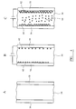
- a material processing apparatus 2 has a twin screw extruder 4 for providing a mixture of an electroluminescent organic semiconductor material, a matrix material such as a polymer, and an ionic material for supplying positive and negative ions for contributing to electrochemical doping of the organic semiconductor material, such that at least the matrix material, and preferably the entire mixture, is in a molten state.
- the molten mixture can then either be solidified into pellets directly from the extruder 4 for subsequent processing at a different location, or fed to a sheet forming unit 6 which forms a sheet 8 of solidified electroluminescent mixture which can then be wound onto a roll 10 by means of a windup unit 12.
- the electroluminescent material is itself an organic semiconductor material, but it will be appreciated by persons skilled in the art that separate electroluminescent materials and organic semiconductor materials can be used.
- inorganic electroluminescent materials for example quantum dot materials such as cadmium sulphide, cadmium selenide, or cadmium selenide and zinc sulphide combinations can be used.
- the extruder 4 comprises a pair of screws 14, 16 mounted for rotation about generally parallel axes 18, 20 respectively within a housing 22 having a series of heaters 24 and temperature sensors 26 to enable the temperature of different zones of the housing to be carefully controlled as the molten mixture is conveyed through the housing 22 by means of the screws 14, 16.
- the housing 22 defines a first feed zone 28 for receiving pellets of polymer matrix material (not shown) via a first inlet 30, and a melt zone 32 in which the polymer matrix material is subjected to shear by interleaved discs 34 of the screws 14, 16 and heated to bring the polymer matrix material to a molten state.
- the profile of the screws 14, 16 is inclined forwards in the first feed zone 28 so that material is conveyed towards the melt zone 32.
- a part 36 of each screw 14, 16 is inclined backwards relative to the direction of propagation, in order to form a melt seal 38 to minimise leakage of molten material from the melt zone 32, and a liquid solution of electroluminescent organic semiconductor material containing ionic material for providing positive and negative ions for contributing to electrochemical doping of the organic semiconductor material dissolved in a suitable solvent such as toluene is injected into the molten polymer matrix material in a second feed zone 40 via a second inlet 42.
- the housing has a mix zone 44 in which the electroluminescent polymer solution and molten polymer matrix material are subjected to shear by means of interleaved discs 46 of the screws 14, 16, and excess solvent can be vented through an outlet 48 and recovered for reuse.
- the molten mixture then passed to an extrusion zone 50 where it is discharged from an extrusion die 52 in the form of pellets or fed into the sheet forming unit 6 to form sheet 8 ( Figure 1 ).
- a light emitting device In order to form a light emitting device from the material generated by the material processing apparatus 2 shown in Figure 1 , material from the previously solidified sheet 8 is dissolved in a suitable solvent such as toluene, or the molten mixture is formed directly from the extruder 4 or via a moulding device (not shown) into a suitable shape.
- a light emitting region 54 is then formed, as shown in greater detail in Figures 4A to 4C , by applying an electric field to the molten mixture by means of suitable electrodes 56, 58, as shown in Figure 4A , in which the ionic material and electroluminescent material is initially distributed relatively uniformly throughout the molten mixture.
- the applied voltage subsequently causes holes to move from the anode 56 towards the cathode 58, and electrons to move from the cathode 58 towards the anode 56, and between the regions 60, 62 of n and p type doping, holes and electrons combine to form neutral pairs 64, which radiatively decay and emit visible light.
- the mixture is allowed to set, as a result of which an excess of negative ions 60 remain located adjacent to the anode 56, and an excess of positive ions 62 remain located adjacent to the cathode 58.
- the electroluminescent device incorporating the light emitting region 54 switches on and off more quickly than a device in which the ionic material is uniformly distributed throughout the light emitting layer 54, since the layers 60, 62 of ions material adjacent to the respective electrodes 56, 58 do not need to be built up by application of a voltage.
- the effect of the layers 60, 62 of ions is to increase the electrical conductivity of the respective regions in which they are located, which in turn has the effect of increasing the proportion of the applied voltage which is applied to the middle region containing the electron/hole pairs 62.
- conductive particles such as indium tin oxide (ITO), gold or aluminium can be distributed in the mixture.
- ITO indium tin oxide
- Particles dispersed in the mixture therefore create multiple light emitting domains. The provision of multiple light emitting domains results in higher current efficiency for very similar voltage requirements.
- Polystyrene pellets were fed into a twin screw extruder 4 at a rate of 0.6gm/minute, and the screws 14, 16 were caused to rotate at a rate of 50rpm.
- the first feed zone 28 of the extruder 4 was maintained at a temperature of 165 degrees C, and the melt zone 32 and liquid feed zone 40 are maintained at a temperature of 172 degrees C.
- the above solution was them pumped into inlet 42 at a rate of 5ml/minute, and the mix zone 44 and extrusion zone 50 were maintained at a temperature of 175 degrees C and the extrusion die 52 at 120 degrees C.
- the extruded film material was then supplied to sheet forming unit 6 and the sheet 8 was then collected from the wind up unit 12 of the material processing apparatus 2.
Landscapes
- Physics & Mathematics (AREA)
- Optics & Photonics (AREA)
- Engineering & Computer Science (AREA)
- Manufacturing & Machinery (AREA)
- Electroluminescent Light Sources (AREA)
Priority Applications (2)
| Application Number | Priority Date | Filing Date | Title |
|---|---|---|---|
| EP11185550.8A EP2584624A1 (fr) | 2011-10-18 | 2011-10-18 | Procédé pour la fabrication de matériau précurseur pour former une région électroluminescente d'un dispositif électroluminescent |
| PCT/GB2012/052568 WO2013057489A1 (fr) | 2011-10-18 | 2012-10-17 | Procédé de fabrication d'un matériau précurseur destiné à former une région électroluminescente d'un dispositif électroluminescent |
Applications Claiming Priority (1)
| Application Number | Priority Date | Filing Date | Title |
|---|---|---|---|
| EP11185550.8A EP2584624A1 (fr) | 2011-10-18 | 2011-10-18 | Procédé pour la fabrication de matériau précurseur pour former une région électroluminescente d'un dispositif électroluminescent |
Publications (1)
| Publication Number | Publication Date |
|---|---|
| EP2584624A1 true EP2584624A1 (fr) | 2013-04-24 |
Family
ID=47049325
Family Applications (1)
| Application Number | Title | Priority Date | Filing Date |
|---|---|---|---|
| EP11185550.8A Withdrawn EP2584624A1 (fr) | 2011-10-18 | 2011-10-18 | Procédé pour la fabrication de matériau précurseur pour former une région électroluminescente d'un dispositif électroluminescent |
Country Status (2)
| Country | Link |
|---|---|
| EP (1) | EP2584624A1 (fr) |
| WO (1) | WO2013057489A1 (fr) |
Cited By (1)
| Publication number | Priority date | Publication date | Assignee | Title |
|---|---|---|---|---|
| WO2021259824A1 (fr) | 2020-06-23 | 2021-12-30 | Merck Patent Gmbh | Procédé de production d'un mélange |
Citations (8)
| Publication number | Priority date | Publication date | Assignee | Title |
|---|---|---|---|---|
| WO1996000983A1 (fr) * | 1994-06-28 | 1996-01-11 | Uniax Corporation | Dispositifs luminescents electrochimiques |
| EP1391944A2 (fr) | 2002-08-21 | 2004-02-25 | Eastman Kodak Company | Ensemble d'éclairage à solide utilisant une couche liquide comprimée |
| WO2006077509A1 (fr) * | 2005-01-21 | 2006-07-27 | Koninklijke Philips Electronics N.V. | Del de polymere |
| EP1686635A1 (fr) * | 2005-01-31 | 2006-08-02 | Samsung SDI Co., Ltd. | Méthode de formation d'un film mince et méthode de fabrication d'une diode organique électroluminescente |
| US20060270100A1 (en) * | 2002-03-08 | 2006-11-30 | International Business Machines Corporation | Low temperature melt-processing of organic-inorganic hybrid |
| EP1965451A1 (fr) * | 2007-02-27 | 2008-09-03 | Samsung Electronics Co., Ltd. | Dispersant pour nanotubes en carbone et composition à nanotubes en carbone le comprenant |
| EP2017306A1 (fr) * | 2006-03-23 | 2009-01-21 | Toray Industries, Inc. | Formule de résine thermoplastique, son procédé de production et moulage |
| EP2381503A1 (fr) * | 2010-04-23 | 2011-10-26 | Polyphotonix Limited | Procédé et appareil pour la fabrication de matériau pour une utilisation pour la fabrication de dispositifs semi-conducteurs organiques |
Family Cites Families (2)
| Publication number | Priority date | Publication date | Assignee | Title |
|---|---|---|---|---|
| WO2006011090A1 (fr) * | 2004-07-21 | 2006-02-02 | Koninklijke Philips Electronics N.V. | Cellule lumineuse electrochimique |
| WO2008045122A2 (fr) * | 2006-10-05 | 2008-04-17 | The Regents Of The University Of California | Dispositifs électroluminescents polymères hybrides |
-
2011
- 2011-10-18 EP EP11185550.8A patent/EP2584624A1/fr not_active Withdrawn
-
2012
- 2012-10-17 WO PCT/GB2012/052568 patent/WO2013057489A1/fr active Application Filing
Patent Citations (8)
| Publication number | Priority date | Publication date | Assignee | Title |
|---|---|---|---|---|
| WO1996000983A1 (fr) * | 1994-06-28 | 1996-01-11 | Uniax Corporation | Dispositifs luminescents electrochimiques |
| US20060270100A1 (en) * | 2002-03-08 | 2006-11-30 | International Business Machines Corporation | Low temperature melt-processing of organic-inorganic hybrid |
| EP1391944A2 (fr) | 2002-08-21 | 2004-02-25 | Eastman Kodak Company | Ensemble d'éclairage à solide utilisant une couche liquide comprimée |
| WO2006077509A1 (fr) * | 2005-01-21 | 2006-07-27 | Koninklijke Philips Electronics N.V. | Del de polymere |
| EP1686635A1 (fr) * | 2005-01-31 | 2006-08-02 | Samsung SDI Co., Ltd. | Méthode de formation d'un film mince et méthode de fabrication d'une diode organique électroluminescente |
| EP2017306A1 (fr) * | 2006-03-23 | 2009-01-21 | Toray Industries, Inc. | Formule de résine thermoplastique, son procédé de production et moulage |
| EP1965451A1 (fr) * | 2007-02-27 | 2008-09-03 | Samsung Electronics Co., Ltd. | Dispersant pour nanotubes en carbone et composition à nanotubes en carbone le comprenant |
| EP2381503A1 (fr) * | 2010-04-23 | 2011-10-26 | Polyphotonix Limited | Procédé et appareil pour la fabrication de matériau pour une utilisation pour la fabrication de dispositifs semi-conducteurs organiques |
Cited By (1)
| Publication number | Priority date | Publication date | Assignee | Title |
|---|---|---|---|---|
| WO2021259824A1 (fr) | 2020-06-23 | 2021-12-30 | Merck Patent Gmbh | Procédé de production d'un mélange |
Also Published As
| Publication number | Publication date |
|---|---|
| WO2013057489A1 (fr) | 2013-04-25 |
Similar Documents
| Publication | Publication Date | Title |
|---|---|---|
| EP1798785B1 (fr) | Electrodes polymériques transparentes pour dispositifs électro-optiques | |
| US10957868B2 (en) | Electron injection based vertical light emitting transistors and methods of making | |
| EP1003229A1 (fr) | Structure pour améliorer la fiabilité des dispositifs électroluminescents organiques et polymères et méthode de fabrication | |
| US10067399B2 (en) | Transmittance-variable film and method for producing same | |
| CN106340533B (zh) | Oled显示面板及其制作方法 | |
| WO2011016725A1 (fr) | Procédé de fabrication dun dispositif optoélectrique | |
| KR20080032128A (ko) | 유기계 장치 및 그 제조 방법 | |
| US20200020891A1 (en) | Oled display panel, manufacturing method thereof, electronic device | |
| KR20130044464A (ko) | 은 나노섬유의 제조방법 및 그 방법에 의해 제조된 은 나노섬유 | |
| GB2528476A (en) | Roll-to-roll processing of a coated web | |
| US10109796B2 (en) | Methods of applying polymers to surfaces and surfaces coated by polymers | |
| EP2584624A1 (fr) | Procédé pour la fabrication de matériau précurseur pour former une région électroluminescente d'un dispositif électroluminescent | |
| WO2010123362A1 (fr) | Dispositif opto-électrique et son procédé de fabrication | |
| US20120075185A1 (en) | Display | |
| JP5414046B2 (ja) | 静電塗布方法及び装置 | |
| US9478765B2 (en) | Electro-optical device stack, having patches covering layer breaches | |
| US11276845B2 (en) | Organic light emitting diodes with silver contacts | |
| US20120074433A1 (en) | Electronic apparatus | |
| JP5474782B2 (ja) | 有機電子デバイスのための改良された印刷カソードのための方法および装置 | |
| KR101439753B1 (ko) | 유연성을 가지는 비정질 투명 전극 소자 | |
| TW201230431A (en) | Light-emitting device and method for manufacturing light-emitting device | |
| US20090246896A1 (en) | Method and apparatus for improved printed cathodes for organic electronic devices | |
| JP2011003442A (ja) | 有機薄膜素子の製造方法 | |
| Koizumi et al. | Effect of drying condition of emitting layer formed by ink-jet coating on optical property and film morphology of polymer-based organic light-emitting diodes | |
| WO2015025474A1 (fr) | Procédé pour fabriquer une électrode transparente, électrode transparente et élément électroluminescent organique comportant ladite électrode |
Legal Events
| Date | Code | Title | Description |
|---|---|---|---|
| PUAI | Public reference made under article 153(3) epc to a published international application that has entered the european phase |
Free format text: ORIGINAL CODE: 0009012 |
|
| AK | Designated contracting states |
Kind code of ref document: A1 Designated state(s): AL AT BE BG CH CY CZ DE DK EE ES FI FR GB GR HR HU IE IS IT LI LT LU LV MC MK MT NL NO PL PT RO RS SE SI SK SM TR |
|
| AX | Request for extension of the european patent |
Extension state: BA ME |
|
| STAA | Information on the status of an ep patent application or granted ep patent |
Free format text: STATUS: THE APPLICATION IS DEEMED TO BE WITHDRAWN |
|
| 18D | Application deemed to be withdrawn |
Effective date: 20131025 |