EP2579310A2 - Einmal programmierbare Vorrichtung mit einer LDMOS-Struktur und dazugehöriges Herstellungsverfahren - Google Patents
Einmal programmierbare Vorrichtung mit einer LDMOS-Struktur und dazugehöriges Herstellungsverfahren Download PDFInfo
- Publication number
- EP2579310A2 EP2579310A2 EP12006108.0A EP12006108A EP2579310A2 EP 2579310 A2 EP2579310 A2 EP 2579310A2 EP 12006108 A EP12006108 A EP 12006108A EP 2579310 A2 EP2579310 A2 EP 2579310A2
- Authority
- EP
- European Patent Office
- Prior art keywords
- programming
- gate
- pass gate
- gate electrode
- dielectric
- Prior art date
- Legal status (The legal status is an assumption and is not a legal conclusion. Google has not performed a legal analysis and makes no representation as to the accuracy of the status listed.)
- Withdrawn
Links
Images


Classifications
-
- H—ELECTRICITY
- H10—SEMICONDUCTOR DEVICES; ELECTRIC SOLID-STATE DEVICES NOT OTHERWISE PROVIDED FOR
- H10D—INORGANIC ELECTRIC SEMICONDUCTOR DEVICES
- H10D30/00—Field-effect transistors [FET]
- H10D30/60—Insulated-gate field-effect transistors [IGFET]
- H10D30/64—Double-diffused metal-oxide semiconductor [DMOS] FETs
- H10D30/65—Lateral DMOS [LDMOS] FETs
-
- H—ELECTRICITY
- H10—SEMICONDUCTOR DEVICES; ELECTRIC SOLID-STATE DEVICES NOT OTHERWISE PROVIDED FOR
- H10B—ELECTRONIC MEMORY DEVICES
- H10B20/00—Read-only memory [ROM] devices
- H10B20/20—Programmable ROM [PROM] devices comprising field-effect components
- H10B20/25—One-time programmable ROM [OTPROM] devices, e.g. using electrically-fusible links
-
- H—ELECTRICITY
- H10—SEMICONDUCTOR DEVICES; ELECTRIC SOLID-STATE DEVICES NOT OTHERWISE PROVIDED FOR
- H10D—INORGANIC ELECTRIC SEMICONDUCTOR DEVICES
- H10D30/00—Field-effect transistors [FET]
- H10D30/01—Manufacture or treatment
- H10D30/021—Manufacture or treatment of FETs having insulated gates [IGFET]
- H10D30/028—Manufacture or treatment of FETs having insulated gates [IGFET] of double-diffused metal oxide semiconductor [DMOS] FETs
- H10D30/0281—Manufacture or treatment of FETs having insulated gates [IGFET] of double-diffused metal oxide semiconductor [DMOS] FETs of lateral DMOS [LDMOS] FETs
-
- H—ELECTRICITY
- H10—SEMICONDUCTOR DEVICES; ELECTRIC SOLID-STATE DEVICES NOT OTHERWISE PROVIDED FOR
- H10D—INORGANIC ELECTRIC SEMICONDUCTOR DEVICES
- H10D84/00—Integrated devices formed in or on semiconductor substrates that comprise only semiconducting layers, e.g. on Si wafers or on GaAs-on-Si wafers
- H10D84/80—Integrated devices formed in or on semiconductor substrates that comprise only semiconducting layers, e.g. on Si wafers or on GaAs-on-Si wafers characterised by the integration of at least one component covered by groups H10D12/00 or H10D30/00, e.g. integration of IGFETs
- H10D84/82—Integrated devices formed in or on semiconductor substrates that comprise only semiconducting layers, e.g. on Si wafers or on GaAs-on-Si wafers characterised by the integration of at least one component covered by groups H10D12/00 or H10D30/00, e.g. integration of IGFETs of only field-effect components
- H10D84/83—Integrated devices formed in or on semiconductor substrates that comprise only semiconducting layers, e.g. on Si wafers or on GaAs-on-Si wafers characterised by the integration of at least one component covered by groups H10D12/00 or H10D30/00, e.g. integration of IGFETs of only field-effect components of only insulated-gate FETs [IGFET]
-
- H—ELECTRICITY
- H10—SEMICONDUCTOR DEVICES; ELECTRIC SOLID-STATE DEVICES NOT OTHERWISE PROVIDED FOR
- H10W—GENERIC PACKAGES, INTERCONNECTIONS, CONNECTORS OR OTHER CONSTRUCTIONAL DETAILS OF DEVICES COVERED BY CLASS H10
- H10W10/00—Isolation regions in semiconductor bodies between components of integrated devices
- H10W10/01—Manufacture or treatment
- H10W10/011—Manufacture or treatment of isolation regions comprising dielectric materials
- H10W10/014—Manufacture or treatment of isolation regions comprising dielectric materials using trench refilling with dielectric materials, e.g. shallow trench isolations
-
- H—ELECTRICITY
- H10—SEMICONDUCTOR DEVICES; ELECTRIC SOLID-STATE DEVICES NOT OTHERWISE PROVIDED FOR
- H10W—GENERIC PACKAGES, INTERCONNECTIONS, CONNECTORS OR OTHER CONSTRUCTIONAL DETAILS OF DEVICES COVERED BY CLASS H10
- H10W10/00—Isolation regions in semiconductor bodies between components of integrated devices
- H10W10/10—Isolation regions comprising dielectric materials
- H10W10/17—Isolation regions comprising dielectric materials formed using trench refilling with dielectric materials, e.g. shallow trench isolations
-
- H—ELECTRICITY
- H10—SEMICONDUCTOR DEVICES; ELECTRIC SOLID-STATE DEVICES NOT OTHERWISE PROVIDED FOR
- H10W—GENERIC PACKAGES, INTERCONNECTIONS, CONNECTORS OR OTHER CONSTRUCTIONAL DETAILS OF DEVICES COVERED BY CLASS H10
- H10W20/00—Interconnections in chips, wafers or substrates
- H10W20/40—Interconnections external to wafers or substrates, e.g. back-end-of-line [BEOL] metallisations or vias connecting to gate electrodes
- H10W20/49—Adaptable interconnections, e.g. fuses or antifuses
- H10W20/491—Antifuses, i.e. interconnections changeable from non-conductive to conductive
-
- H—ELECTRICITY
- H10—SEMICONDUCTOR DEVICES; ELECTRIC SOLID-STATE DEVICES NOT OTHERWISE PROVIDED FOR
- H10B—ELECTRONIC MEMORY DEVICES
- H10B20/00—Read-only memory [ROM] devices
- H10B20/27—ROM only
- H10B20/30—ROM only having the source region and the drain region on the same level, e.g. lateral transistors
- H10B20/34—Source electrode or drain electrode programmed
-
- H—ELECTRICITY
- H10—SEMICONDUCTOR DEVICES; ELECTRIC SOLID-STATE DEVICES NOT OTHERWISE PROVIDED FOR
- H10B—ELECTRONIC MEMORY DEVICES
- H10B20/00—Read-only memory [ROM] devices
- H10B20/27—ROM only
- H10B20/30—ROM only having the source region and the drain region on the same level, e.g. lateral transistors
- H10B20/36—Gate programmed, e.g. different gate material or no gate
- H10B20/363—Gate conductor programmed
-
- H—ELECTRICITY
- H10—SEMICONDUCTOR DEVICES; ELECTRIC SOLID-STATE DEVICES NOT OTHERWISE PROVIDED FOR
- H10B—ELECTRONIC MEMORY DEVICES
- H10B20/00—Read-only memory [ROM] devices
- H10B20/27—ROM only
- H10B20/30—ROM only having the source region and the drain region on the same level, e.g. lateral transistors
- H10B20/36—Gate programmed, e.g. different gate material or no gate
- H10B20/367—Gate dielectric programmed, e.g. different thickness
-
- H—ELECTRICITY
- H10—SEMICONDUCTOR DEVICES; ELECTRIC SOLID-STATE DEVICES NOT OTHERWISE PROVIDED FOR
- H10B—ELECTRONIC MEMORY DEVICES
- H10B20/00—Read-only memory [ROM] devices
- H10B20/27—ROM only
- H10B20/30—ROM only having the source region and the drain region on the same level, e.g. lateral transistors
- H10B20/38—Doping programmed, e.g. mask ROM
- H10B20/387—Source region or drain region doping programmed
-
- H—ELECTRICITY
- H10—SEMICONDUCTOR DEVICES; ELECTRIC SOLID-STATE DEVICES NOT OTHERWISE PROVIDED FOR
- H10D—INORGANIC ELECTRIC SEMICONDUCTOR DEVICES
- H10D30/00—Field-effect transistors [FET]
- H10D30/60—Insulated-gate field-effect transistors [IGFET]
- H10D30/601—Insulated-gate field-effect transistors [IGFET] having lightly-doped drain or source extensions, e.g. LDD IGFETs or DDD IGFETs
- H10D30/603—Insulated-gate field-effect transistors [IGFET] having lightly-doped drain or source extensions, e.g. LDD IGFETs or DDD IGFETs having asymmetry in the channel direction, e.g. lateral high-voltage MISFETs having drain offset region or extended drain IGFETs [EDMOS]
-
- H—ELECTRICITY
- H10—SEMICONDUCTOR DEVICES; ELECTRIC SOLID-STATE DEVICES NOT OTHERWISE PROVIDED FOR
- H10D—INORGANIC ELECTRIC SEMICONDUCTOR DEVICES
- H10D64/00—Electrodes of devices having potential barriers
- H10D64/60—Electrodes characterised by their materials
- H10D64/66—Electrodes having a conductor capacitively coupled to a semiconductor by an insulator, e.g. MIS electrodes
- H10D64/665—Electrodes having a conductor capacitively coupled to a semiconductor by an insulator, e.g. MIS electrodes the conductor comprising a layer of elemental metal contacting the insulator, e.g. tungsten or molybdenum
-
- H—ELECTRICITY
- H10—SEMICONDUCTOR DEVICES; ELECTRIC SOLID-STATE DEVICES NOT OTHERWISE PROVIDED FOR
- H10D—INORGANIC ELECTRIC SEMICONDUCTOR DEVICES
- H10D64/00—Electrodes of devices having potential barriers
- H10D64/60—Electrodes characterised by their materials
- H10D64/66—Electrodes having a conductor capacitively coupled to a semiconductor by an insulator, e.g. MIS electrodes
- H10D64/667—Electrodes having a conductor capacitively coupled to a semiconductor by an insulator, e.g. MIS electrodes the conductor comprising a layer of alloy material, compound material or organic material contacting the insulator, e.g. TiN workfunction layers
-
- H—ELECTRICITY
- H10—SEMICONDUCTOR DEVICES; ELECTRIC SOLID-STATE DEVICES NOT OTHERWISE PROVIDED FOR
- H10D—INORGANIC ELECTRIC SEMICONDUCTOR DEVICES
- H10D64/00—Electrodes of devices having potential barriers
- H10D64/60—Electrodes characterised by their materials
- H10D64/66—Electrodes having a conductor capacitively coupled to a semiconductor by an insulator, e.g. MIS electrodes
- H10D64/68—Electrodes having a conductor capacitively coupled to a semiconductor by an insulator, e.g. MIS electrodes characterised by the insulator, e.g. by the gate insulator
- H10D64/691—Electrodes having a conductor capacitively coupled to a semiconductor by an insulator, e.g. MIS electrodes characterised by the insulator, e.g. by the gate insulator comprising metallic compounds, e.g. metal oxides or metal silicates
Definitions
- the present invention is generally in the field of semiconductors. More particularly, the present invention is in the field of one-time programmable semiconductor devices.
- One-time programmable (OTP) devices are used throughout the semiconductor industry to allow for post-fabrication design changes in integrated circuits (ICs). For example, after post-fabrication functionality testing but before sale to a customer, a semiconductor device manufacturer can program a network of OTP devices embedded in a particular semiconductor die to provide a permanent serial number encoding for that particular die. Under other circumstances, a single OTP device can be programmed to permanently enable or disable a portion of an integrated circuit at any time after fabrication, including after sale to a customer. Although this functionality is in great demand, conventional OTP elements (the programmable constituent of an OTP device) can be larger than desired or can require multiple additional fabrication steps beyond those required for conventional transistor fabrication, for example, making conventional OTP devices expensive to manufacture and embed.
- One such conventional embedded OTP device can be fabricated using the so-called split-channel approach, where an atypical metal-oxide-semiconductor field-effect transistor (MOSFET) fabrication process is used to form a gate structure comprising a single channel interface with two different gate dielectric thicknesses.
- MOSFET metal-oxide-semiconductor field-effect transistor
- the thin portion of gate dielectric can be made to destructively break down and form a conductive path from gate to channel, thereby switching the conventional OTP device into a "programmed" state.
- This approach however, has a relatively high tendency to result in devices with programmed states where the remaining thick gate structure exhibits a high leakage current due to collateral damage during programming.
- a one-time programmable (OTP) device having a lateral diffused metal-oxide-semiconductor (LDMOS) structure and related method, substantially as shown in and/or described in connection with at least one of the figures, and as set forth more completely in the claims.
- OTP lateral diffused metal-oxide-semiconductor
- a one-time programmable (OTP) device having a lateral diffused metal-oxide-semiconductor (LDMOS) structure, said OTP device comprising:
- said pass gate and said programming gate are fabricated concurrently.
- said pass gate dielectric and said programming gate dielectric comprise a same dielectric material.
- said programming gate electrode and said pass gate electrode comprise a same electrically conductive material.
- said programming gate electrode makes Schottky contact with said drain extension region after application of said programming voltage.
- said OTP device is an n-channel metal-oxide-semiconductor (NMOS) device.
- NMOS metal-oxide-semiconductor
- said OTP device is a p-channel metal-oxide-semiconductor (PMOS) device.
- PMOS metal-oxide-semiconductor
- said programming gate electrode is formed from a gate metal and said programming gate dielectric comprises a high- ⁇ dielectric.
- the OTP device further comprises an isolation body between said pass gate and said programming gate.
- said isolation body comprises a shallow trench isolation (STI).
- STI shallow trench isolation
- a method for producing a one-time programmable (OTP) device having a lateral diffused metal-oxide-semiconductor (LDMOS) structure comprises:
- said pass gate and said programming gate are fabricated concurrently.
- said pass gate dielectric and said programming gate dielectric are formed of a same dielectric material.
- said programming gate electrode and said pass gate electrode are formed of a same electrically conductive material.
- said programming gate electrode is configured to make Schottky contact with said drain extension region after application of said programming voltage.
- said programming gate electrode is formed from a gate metal and said programming gate dielectric comprises a high- ⁇ dielectric.
- said OTP device is an n-channel metal-oxide-semiconductor (NMOS) device.
- NMOS metal-oxide-semiconductor
- said OTP device is a p-channel metal-oxide-semiconductor (PMOS) device.
- PMOS metal-oxide-semiconductor
- the method further comprises forming an isolation body between said pass gate and said programming gate.
- forming said isolation body between said pass gate and said programming gate comprises forming a shallow trench isolation (STI) between said pass gate and said programming gate.
- STI shallow trench isolation
- the present invention is directed to a one-time programmable (OTP) device having a lateral diffused metal-oxide-semiconductor (LDMOS) structure and related method.
- OTP one-time programmable
- LDMOS lateral diffused metal-oxide-semiconductor
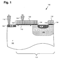
- FIG. 1 shows a cross-sectional view of OTP device 100 having LDMOS structure 101, according to one embodiment of the present invention, capable of overcoming the drawbacks and deficiencies associated with the conventional art.
- OTP device 100 which is represented as an n-channel metal-oxide-semiconductor (NMOS) device in Figure 1 , can be fabricated in P type semiconductor body 102, which may comprise a portion of a Group IV semiconductor wafer or die, such as a wafer or die comprising silicon or germanium, for example.
- Semiconductor body 102 may include N type drain extension region 104, heavily doped N+ drain region 106, and heavily doped N+ source region 108.
- OTP device 100 may comprise pass gate 120 including pass gate electrode 122 and pass gate dielectric 124, and programming gate 130 including programming gate electrode 132 and programming gate dielectric 134.
- pass gate 120 is formed over channel region 110 of semiconductor body, while programming gate 130 is spaced from pass gate 120 by a portion of drain extension region 104.
- bit line contact 116 formed over heavily doped source region 108 and word line contact 126 formed over pass gate 120.
- OTP device 100 is configured to have enhanced programming reliability while concurrently providing protection for pass gate 120 when a programming voltage for rupturing programming gate dielectric 134 is applied to programming gate electrode 132.
- programming gate 130 may be fabricated using a high- ⁇ metal gate process, such that, after programming, a Schottky contact is formed between programming gate electrode 132 and drain extension region 104, thereby enabling better conduction in a forward biased state.
- OTP device 100 can be fabricated alongside conventional CMOS devices, and may be monolithically integrated with CMOS logic, for example, in an integrated circuit (IC) fabricated on a semiconductor wafer or die.
- CMOS complementary metal-oxide-semiconductor
- an OTP device characterizes OTP device 100 as an NMOS device
- an OTP device according to the present inventive principles can comprise an n-channel or p-channel MOSFET, and thus may be implemented as a PMOS device, as well as the example NMOS device shown specifically as OTP device 100, in Figure 1 .
- FIG. 2 shows flowchart 200 presenting one embodiment of a method for producing an OTP device having an LDMOS structure
- Figure 3 shows OTP device 300 corresponding to OTP device 100, in Figure 1 , after programming, according to one embodiment of the present invention.
- flowchart 200 in Figure 2 , it is noted that certain details and features have been left out of flowchart 200 that are apparent to a person of ordinary skill in the art.
- a step may comprise one or more substeps or may involve specialized equipment or materials, as known in the art.
- steps 210 through 240 indicated in flowchart 200 are sufficient to describe one embodiment of the present invention, other embodiments of the present invention may utilize steps different from those shown in flowchart 200, or may comprise more, or fewer, steps.
- step 210 of flowchart 200 comprises forming drain extension region 104 of LDMOS structure 101.
- step 210 may correspond to implanting drain extension region 104 by performing a retrograde implant of dopants into semiconductor body 102.
- the fabrication method of flowchart 200 may be implemented using existing CMOS fabrication process flows.
- OTP device 100 having LDMOS structure 101 may be fabricated on a wafer concurrently undergoing CMOS logic fabrication.
- step 210 may correspond to implanting drain extension region 104 by performing one of a Core Well implant or an IO Well implant procedure, as known in the art.
- step 220 of flowchart 200 comprises fabricating pass gate 120 including pass gate electrode 122 and pass gate dielectric 124 over a first portion of drain extension region 104.
- pass gate 120 including pass gate electrode 122 and pass gate dielectric 124 is situated over channel region 110 and a first portion of drain extension region 104 disposed between channel region 110 and heavily doped drain region 106.
- Pass gate dielectric 124 can be, for example, a high dielectric constant (high- ⁇ ) gate dielectric layer (e.g. a high- ⁇ dielectric layer that can be utilized for forming an NMOS or PMOS gate dielectric).
- high- ⁇ pass gate dielectric 124 can comprise, for example, a metal oxide such as hafnium oxide (HfO 2 ), zirconium oxide (ZrO 2 ), or the like.
- pass gate dielectric 124 can be formed, for example, by depositing a high- ⁇ dielectric material, such as HfO 2 or ZrO 2 , over semiconductor body 102 by utilizing a physical vapor deposition (PVD) process, a chemical vapor deposition (CVD) process, or other suitable process, such as atomic layer deposition (ALD) or molecular beam epitaxy (MBE), for example.
- PVD physical vapor deposition
- CVD chemical vapor deposition
- MBE molecular beam epitaxy
- Pass gate electrode 122 may comprise a gate metal.
- pass gate electrode 122 may be formed from any gate metal suitable for use in an NMOS device, such as tantalum (Ta), tantalum nitride (TaN), or titanium nitride (TiN), for example.
- NMOS device such as tantalum (Ta), tantalum nitride (TaN), or titanium nitride (TiN), for example.
- pass gate electrode 122 may be formed from any gate metal suitable for use in a PMOS device, such as molybdenum (Mo), ruthenium (Ru), or tantalum carbide nitride (TaCN), for example.
- a gate metal provided over pass gate dielectric 124 to produce pass gate electrode 122 can be formed using any of PVD, CVD, ALD, or MBE, for example.
- step 230 of flowchart 200 comprises fabricating programming gate 130 including programming gate electrode 132 and programming gate dielectric 134 over a second portion of drain extension region 104.
- programming gate 130 including programming gate electrode 132 and programming gate dielectric 134 does not adjoin pass gate 120, but rather is situated adjacent pass gate 120 over a second portion of drain extension region 104 spaced apart from the first portion of drain extension region 104 over which pass gate 120 is disposed.
- pass gate 120 and programming gate 130 can be fabricated substantially concurrently. That is to say, steps 220 and 230 of flowchart 200 may be performed concurrently. Moreover, pass gate 120 and programming gate 130 may be formed using substantially the same materials. In other words, pass gate dielectric 124 and programming gate dielectric 134 can comprise the same dielectric material, such as the same high- ⁇ dielectric material, while pass gate electrode 122 and programming gate electrode 132 can comprise the same electrically conductive material, such as the same gate metal.
- fabrication of programming gate 130 can be performed using a high- ⁇ dielectric as programming gate dielectric 134, such as HfO 2 or ZrO 2 , and using a metal gate comprised of Ta, TaN, TiN, Mo, Ru, or TaCN, for example, to implement programming gate electrode 132.
- programming gate 130 like pass gate 120 can be formed using any suitable process, such as PVD, CVD, ALD, or MBE, for example.
- step 240 of flowchart 200 comprises applying a programming voltage to programming gate electrode 132 to rupture programming gate dielectric 134.
- the result of performing step 240 of flowchart 200 on OTP device 100, in Figure 1 is shown in Figure 3 , which presents a cross-sectional view of OTP device 300 having LDMOS structure 301.
- OTP device 300 is shown to include N type drain extension region 304, heavily doped N+ drain region 306, heavily doped N+ source region 308, and channel region 310 in P type semiconductor body 302.
- OTP device 300 also comprises pass gate 320 including pass gate electrode 322 and pass gate dielectric 324, and programming gate 330 including programming gate electrode 332 and programming gate dielectric 334.
- OTP device 300 formed in semiconductor body 302 and comprising pass gate 320 and programming gate 330 corresponds to OTP device 100 formed in semiconductor body 102 and comprising pass gate 120 and programming gate 130, in Figure 1 , after application of a programming voltage to programming gate electrode 132, as indicated by rupture 336 through programming gate dielectric 334, in Figure 3 .
- bit line contact 316 and word line contact 326 are also shown in Figure 3 .
- Step 240 of flowchart 200 may be performed through application of a relatively high voltage, such as an approximately 5 volt programming voltage, for example, to programming gate electrode 332, to produce one or more pinhole type rupture(s) 336 in programming gate dielectric 334.
- a relatively high voltage such as an approximately 5 volt programming voltage
- step 240 results in programming gate electrode 332 making Schottky contact with drain extension region 304.
- pass gate dielectric 324 will remain substantially unaffected by the application of the programming voltage causing pinhole type rupture(s) 336 through programming gate dielectric 334.
- FIG. 4 shows a cross-sectional view of OTP device 400 having LDMOS structure 401, according to another embodiment of the present invention.
- OTP device 400 includes N type drain extension region 404, heavily doped N+ source region 408, and channel region 410 in P type semiconductor body 402.
- OTP device 400 also comprises pass gate 420 including pass gate electrode 422 and pass gate dielectric 424, and programming gate 430 including programming gate electrode 432 and programming gate dielectric 434 through which pinhole type rupture 436 has been formed.
- OTP device 400 formed in semiconductor body 402 and comprising pass gate 420 and programming gate 430 including rupture 416 corresponds to OTP device 300 formed in semiconductor body 302 and comprising pass gate 320 and programming gate 330 including rupture 336, in Figure 3 .
- rupture 436 through programming gate dielectric 434 results in N type drain extension region 404 being in Schottky contact with programming gate electrode 432, when programming gate 430 is fabricated using a high- ⁇ metal gate process.
- Figure 4 shows bit line contact 416 and word line contact 426, corresponding respectively to bit line contact 316 and word line contact 326, in Figure 3 .
- isolation body 418 between pass gate 420 and programming gate 430 having no analogue in the previous figures.
- Isolation body 418 may comprise a shallow trench isolation (STI) structure, such as an STI structure formed of silicon oxide (SiO 2 ), for example, and may be formed according to known CMOS fabrication process steps.
- isolation body 418 may be implemented as part of LDMOS structure 401 to provide additional protection for pass gate 420 when the programming voltage for producing rupture 436 is applied to programming gate electrode 432.
- embodiments of the OTP device disclosed by the present application are configured to withstand higher programming voltages than would otherwise be the case, thereby rendering programming more reliable while advantageously providing enhanced protection for a pass gate portion of the OTP device.
- a programming gate of embodiments of the disclosed OTP device may be fabricated using a high- ⁇ metal gate process, such that, after programming, a Schottky contact is formed between a programming gate electrode and a drain region of the OTP device, thereby enabling improved conduction in a forward biased state.
- the advantages associated with this approach can be realized using existing high- ⁇ metal gate CMOS process flows, making integration of high voltage devices and CMOS core and IO devices on a common IC efficient and cost effective.
- the present invention improves design flexibility without adding cost or complexity to established semiconductor device fabrication processes.
Landscapes
- Metal-Oxide And Bipolar Metal-Oxide Semiconductor Integrated Circuits (AREA)
- Insulated Gate Type Field-Effect Transistor (AREA)
- Semiconductor Memories (AREA)
Applications Claiming Priority (1)
| Application Number | Priority Date | Filing Date | Title |
|---|---|---|---|
| US13/252,880 US8493767B2 (en) | 2011-10-04 | 2011-10-04 | One-time programmable device having an LDMOS structure |
Publications (2)
| Publication Number | Publication Date |
|---|---|
| EP2579310A2 true EP2579310A2 (de) | 2013-04-10 |
| EP2579310A3 EP2579310A3 (de) | 2013-09-04 |
Family
ID=47022437
Family Applications (1)
| Application Number | Title | Priority Date | Filing Date |
|---|---|---|---|
| EP12006108.0A Withdrawn EP2579310A3 (de) | 2011-10-04 | 2012-08-28 | Einmal programmierbare Vorrichtung mit einer LDMOS-Struktur und dazugehöriges Herstellungsverfahren |
Country Status (4)
| Country | Link |
|---|---|
| US (3) | US8493767B2 (de) |
| EP (1) | EP2579310A3 (de) |
| CN (1) | CN103035647B (de) |
| TW (1) | TWI499007B (de) |
Families Citing this family (3)
| Publication number | Priority date | Publication date | Assignee | Title |
|---|---|---|---|---|
| CN104600073B (zh) * | 2013-10-30 | 2017-06-06 | 上海华虹宏力半导体制造有限公司 | Otp器件及制造方法 |
| US11527541B2 (en) * | 2019-12-31 | 2022-12-13 | Taiwan Semiconductoh Manufactuhing Company Limited | System and method for reducing resistance in anti-fuse cell |
| CN112234094B (zh) * | 2020-09-29 | 2022-07-29 | 矽力杰半导体技术(杭州)有限公司 | 金属氧化物半导体器件及其制造方法 |
Family Cites Families (7)
| Publication number | Priority date | Publication date | Assignee | Title |
|---|---|---|---|---|
| US5909049A (en) * | 1997-02-11 | 1999-06-01 | Actel Corporation | Antifuse programmed PROM cell |
| US8264039B2 (en) * | 2004-04-26 | 2012-09-11 | Synopsys, Inc. | High-voltage LDMOSFET and applications therefor in standard CMOS |
| US7795094B2 (en) * | 2004-09-02 | 2010-09-14 | Micron Technology, Inc. | Recessed gate dielectric antifuse |
| US7553704B2 (en) * | 2005-06-28 | 2009-06-30 | Freescale Semiconductor, Inc. | Antifuse element and method of manufacture |
| US20080296701A1 (en) * | 2007-05-29 | 2008-12-04 | Ememory Technology Inc. | One-time programmable read-only memory |
| KR100979098B1 (ko) * | 2008-06-20 | 2010-08-31 | 주식회사 동부하이텍 | 반도체 소자 및 이를 위한 otp 셀 형성 방법 |
| US8178944B2 (en) * | 2009-06-22 | 2012-05-15 | Broadcom Corporation | Method for forming a one-time programmable metal fuse and related structure |
-
2011
- 2011-10-04 US US13/252,880 patent/US8493767B2/en active Active
-
2012
- 2012-08-28 EP EP12006108.0A patent/EP2579310A3/de not_active Withdrawn
- 2012-09-12 TW TW101133331A patent/TWI499007B/zh not_active IP Right Cessation
- 2012-09-28 CN CN201210371702.1A patent/CN103035647B/zh not_active Expired - Fee Related
-
2013
- 2013-07-18 US US13/945,535 patent/US8932912B2/en not_active Expired - Fee Related
- 2013-07-18 US US13/945,739 patent/US8969957B2/en active Active
Non-Patent Citations (1)
| Title |
|---|
| None |
Also Published As
| Publication number | Publication date |
|---|---|
| CN103035647B (zh) | 2016-12-07 |
| US20130302960A1 (en) | 2013-11-14 |
| EP2579310A3 (de) | 2013-09-04 |
| US20130082325A1 (en) | 2013-04-04 |
| US8493767B2 (en) | 2013-07-23 |
| CN103035647A (zh) | 2013-04-10 |
| TW201324691A (zh) | 2013-06-16 |
| US8932912B2 (en) | 2015-01-13 |
| US20130299904A1 (en) | 2013-11-14 |
| TWI499007B (zh) | 2015-09-01 |
| US8969957B2 (en) | 2015-03-03 |
Similar Documents
| Publication | Publication Date | Title |
|---|---|---|
| US8923070B2 (en) | FinFET based one-time programmable device | |
| TWI493555B (zh) | 電子系統、反熔絲記憶體元件及其提供方法 | |
| US9799751B1 (en) | Methods of forming a gate structure on a vertical transistor device | |
| US9178036B1 (en) | Methods of forming transistor devices with different threshold voltages and the resulting products | |
| TWI508251B (zh) | 包括具有提升之程式化效率性之電子熔絲的半導體裝置及其形成的方法 | |
| US8455977B2 (en) | Programmable fuse | |
| US9536883B2 (en) | Dual anti-fuse | |
| US9257440B2 (en) | Non-volatile anti-fuse with consistent rupture | |
| US8932912B2 (en) | One-time programmable device | |
| US20130009231A1 (en) | Method for Efficiently Fabricating Memory Cells with Logic FETs and Related Structure | |
| US8766374B2 (en) | One-time programmable semiconductor device | |
| US8937357B2 (en) | One-time programmable semiconductor device | |
| US20140038404A1 (en) | Flash Memory Utilizing a High-K Metal Gate | |
| US8390063B2 (en) | Semiconductor device having a lightly doped semiconductor gate and method for fabricating same | |
| HK1180111A (en) | One-time programmable device having an ldmos structure and related method | |
| US9276004B2 (en) | ROM arrays having memory cell transistors programmed using metal gates | |
| WO2015026985A1 (en) | Method and apparatus for suppressing metal-gate cross-diffusion in semiconductor technology | |
| US7812408B1 (en) | Integrated circuits with metal-oxide-semiconductor transistors having enhanced gate depletion layers | |
| HK1178316B (en) | Finfet based one-time programmable device and related method |
Legal Events
| Date | Code | Title | Description |
|---|---|---|---|
| PUAI | Public reference made under article 153(3) epc to a published international application that has entered the european phase |
Free format text: ORIGINAL CODE: 0009012 |
|
| 17P | Request for examination filed |
Effective date: 20120828 |
|
| AK | Designated contracting states |
Kind code of ref document: A2 Designated state(s): AL AT BE BG CH CY CZ DE DK EE ES FI FR GB GR HR HU IE IS IT LI LT LU LV MC MK MT NL NO PL PT RO RS SE SI SK SM TR |
|
| AX | Request for extension of the european patent |
Extension state: BA ME |
|
| RIN1 | Information on inventor provided before grant (corrected) |
Inventor name: ITO, AKIRA Inventor name: CHEN, XIANGDONG |
|
| PUAL | Search report despatched |
Free format text: ORIGINAL CODE: 0009013 |
|
| AK | Designated contracting states |
Kind code of ref document: A3 Designated state(s): AL AT BE BG CH CY CZ DE DK EE ES FI FR GB GR HR HU IE IS IT LI LT LU LV MC MK MT NL NO PL PT RO RS SE SI SK SM TR |
|
| AX | Request for extension of the european patent |
Extension state: BA ME |
|
| RIC1 | Information provided on ipc code assigned before grant |
Ipc: H01L 27/112 20060101AFI20130730BHEP Ipc: H01L 29/78 20060101ALI20130730BHEP Ipc: H01L 29/51 20060101ALI20130730BHEP Ipc: H01L 29/49 20060101ALI20130730BHEP Ipc: H01L 23/525 20060101ALI20130730BHEP |
|
| 17Q | First examination report despatched |
Effective date: 20130819 |
|
| RBV | Designated contracting states (corrected) |
Designated state(s): AL AT BE BG CH CY CZ DE DK EE ES FI FR GB GR HR HU IE IS IT LI LT LU LV MC MK MT NL NO PL PT RO RS SE SI SK SM TR |
|
| RAP1 | Party data changed (applicant data changed or rights of an application transferred) |
Owner name: AVAGO TECHNOLOGIES GENERAL IP (SINGAPORE) PTE. LTD |
|
| RAP1 | Party data changed (applicant data changed or rights of an application transferred) |
Owner name: AVAGO TECHNOLOGIES INTERNATIONAL SALES PTE. LIMITE |
|
| GRAP | Despatch of communication of intention to grant a patent |
Free format text: ORIGINAL CODE: EPIDOSNIGR1 |
|
| STAA | Information on the status of an ep patent application or granted ep patent |
Free format text: STATUS: GRANT OF PATENT IS INTENDED |
|
| INTG | Intention to grant announced |
Effective date: 20200504 |
|
| STAA | Information on the status of an ep patent application or granted ep patent |
Free format text: STATUS: THE APPLICATION IS DEEMED TO BE WITHDRAWN |
|
| 18D | Application deemed to be withdrawn |
Effective date: 20200915 |