EP2575265A1 - Signaux de commande en forme dans des dispositifs de communication en champ proche (NFC) - Google Patents
Signaux de commande en forme dans des dispositifs de communication en champ proche (NFC) Download PDFInfo
- Publication number
- EP2575265A1 EP2575265A1 EP12005708A EP12005708A EP2575265A1 EP 2575265 A1 EP2575265 A1 EP 2575265A1 EP 12005708 A EP12005708 A EP 12005708A EP 12005708 A EP12005708 A EP 12005708A EP 2575265 A1 EP2575265 A1 EP 2575265A1
- Authority
- EP
- European Patent Office
- Prior art keywords
- signal
- control signal
- nfc device
- shaped
- nfc
- Prior art date
- Legal status (The legal status is an assumption and is not a legal conclusion. Google has not performed a legal analysis and makes no representation as to the accuracy of the status listed.)
- Withdrawn
Links
- 238000004891 communication Methods 0.000 title claims abstract description 29
- 238000000034 method Methods 0.000 claims description 16
- 238000007493 shaping process Methods 0.000 claims description 9
- 230000004044 response Effects 0.000 claims description 4
- 239000010752 BS 2869 Class D Substances 0.000 description 7
- 230000008569 process Effects 0.000 description 6
- 238000010586 diagram Methods 0.000 description 5
- 238000004590 computer program Methods 0.000 description 4
- 239000003990 capacitor Substances 0.000 description 2
- 230000000694 effects Effects 0.000 description 2
- 230000006978 adaptation Effects 0.000 description 1
- 238000013461 design Methods 0.000 description 1
- 230000008030 elimination Effects 0.000 description 1
- 238000003379 elimination reaction Methods 0.000 description 1
- 230000005669 field effect Effects 0.000 description 1
- 238000012986 modification Methods 0.000 description 1
- 230000004048 modification Effects 0.000 description 1
- 230000002093 peripheral effect Effects 0.000 description 1
- 238000012545 processing Methods 0.000 description 1
- 230000001105 regulatory effect Effects 0.000 description 1
- 239000000126 substance Substances 0.000 description 1
- 230000007704 transition Effects 0.000 description 1
Images


Classifications
-
- H—ELECTRICITY
- H04—ELECTRIC COMMUNICATION TECHNIQUE
- H04B—TRANSMISSION
- H04B5/00—Near-field transmission systems, e.g. inductive or capacitive transmission systems
- H04B5/70—Near-field transmission systems, e.g. inductive or capacitive transmission systems specially adapted for specific purposes
-
- H—ELECTRICITY
- H03—ELECTRONIC CIRCUITRY
- H03C—MODULATION
- H03C7/00—Modulating electromagnetic waves
-
- H—ELECTRICITY
- H04—ELECTRIC COMMUNICATION TECHNIQUE
- H04B—TRANSMISSION
- H04B5/00—Near-field transmission systems, e.g. inductive or capacitive transmission systems
- H04B5/40—Near-field transmission systems, e.g. inductive or capacitive transmission systems characterised by components specially adapted for near-field transmission
- H04B5/48—Transceivers
-
- Y—GENERAL TAGGING OF NEW TECHNOLOGICAL DEVELOPMENTS; GENERAL TAGGING OF CROSS-SECTIONAL TECHNOLOGIES SPANNING OVER SEVERAL SECTIONS OF THE IPC; TECHNICAL SUBJECTS COVERED BY FORMER USPC CROSS-REFERENCE ART COLLECTIONS [XRACs] AND DIGESTS
- Y02—TECHNOLOGIES OR APPLICATIONS FOR MITIGATION OR ADAPTATION AGAINST CLIMATE CHANGE
- Y02D—CLIMATE CHANGE MITIGATION TECHNOLOGIES IN INFORMATION AND COMMUNICATION TECHNOLOGIES [ICT], I.E. INFORMATION AND COMMUNICATION TECHNOLOGIES AIMING AT THE REDUCTION OF THEIR OWN ENERGY USE
- Y02D30/00—Reducing energy consumption in communication networks
- Y02D30/70—Reducing energy consumption in communication networks in wireless communication networks
Definitions
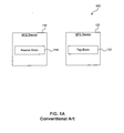
- Fig. 1A shows a conventional communication system 100 including two NFC devices 110, 120 for communicating with each other.
- NFC device 110 includes a Reader block 114 and the NFC device 120 includes a Tag block 122, along with other supporting circuitry (not shown).
- the communication between the NFC devices 110, 120 is initiated when an antenna driver included in a Reader block drives an antenna of one of the NFC devices to output a magnetic field that can power a Tag block included in the other NFC device.
- the communication is established when the powered Tag block modulates the magnetic field with a communications signal and transmits the modulated signal to the Reader block.
- the Reader block 114 includes an antenna driver that drives an antenna associated with the NFC device 110 to output a magnetic field that powers the Tag block 122 included in the NFC device 120.
- the communication is established when the Tag block 122 is powered by the output magnetic field, and when Tag block 122 modulates the magnetic field with a communications signal and transmits the modulated signal back to Reader block 114.
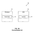
- the NFC device 110 may communicate with a Radio-Frequency Identification (RFID) device.
- RFID Radio-Frequency Identification
- the RFID device 130 includes a Tag 134 and other supporting circuitry (not shown).
- the communication between the NFC device 110 and the RFID device 130 is similar to the communication between the NFC device 110 and the NFC device 120 discussed above.
- the Reader block 114 includes an antenna driver that drives an antenna associated with the NFC device 110 to output a magnetic field that powers the Tag block 134 included in the RFID device 130.
- the communication is established when the Tag block 134 is powered by the output magnetic field, and when Tag block 134 modulates the magnetic field with a communications signal and transmits the modulated signal back to Reader block 114.
- the RFID device 130 can be similar to a RFID device according to ISO 14443, ISO 15693, or a contactless RFID smart card.
- the NFC device 120 and the RFID 130 function in a tag emulator mode while communicating with the NFC device 110.
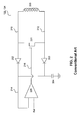
- the error amplifier 205 Based on the results of the comparison, the error amplifier 205 outputs signal 216 to adjust the operation of the FET 201, which is functioning as the shunt regulator.
- the FET 201 Upon receiving signal 216, the FET 201 regulates and clamps the waveform which drives the antenna 200. However, when the FET 201 regulates and clamps the waveform, the FET 201 dissipates a lot of energy (by sinking current) and thereby distorts the waveform. The distortion of the waveform which drives the antenna 200 results in undesired out-of band emissions which interfere with other peripheral radio communication.
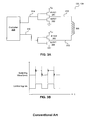
- a class-D amplifier configuration be used to drive the antenna 200. This configuration is shown in Fig. 3A .
- the switching on and off of the FETs 301, 302, 303, 304 using signals 314, 316 is very abrupt. This abrupt switching on and off significantly distorts the switching waveform which drives the antenna 300, and thereby exacerbates the out-of-band emissions.
- the waveform shaper comprises:
- a method for minimizing undesired out-of-band emissions in a near field communication (NFC) device comprises:
- the shaping the control signal comprises:
- the shaping shapes the control signal to minimize variations in the switching waveform.
- FIG. 4A illustrates an exemplaryblock diagram of a Tag block according to an embodiment of the present invention.
- FIG. 4B illustrates an exemplary representation of input and output waveforms generated by the Tag block illustrated in Fig. 4A according to an embodiment of the present invention.
- the conventional configurations of the Tag block 122, 134 are unable to minimize the undesired out-of-band emissions without dissipating a lot of power.
- the present invention minimizes the undesired out-of-band emissions without dissipating a lot of power, as shown in Fig. 4A .
- the inventive configuration of the Tag block includes an antenna 400 having differential signals 410, 412, P-FETs 401, 403 and N-FETs 402, 404 forming the class-D amplifier configuration, shaped signals 414, 416, 418, 420, the waveform shaper 406, controller signals 422, 424, the controller 405, rectifying diodes 407, 408 to output a rectified signal 426, and a capacitor 409.
- the antenna 400 detects the magnetic field output by a Reader block of another NFC device, and provides differential signals 410, 412. These differential signals 410, 412 are rectified by rectifying diodes 407, 408 to produce the rectified signal 426.
- the rectified signal 426 is received by the controller and compared to a reference signal 428.
- the reference signal is associated with a strength of the magnetic field detected by the antenna 400.
- the controller 405 compares the rectified signal 426 with the reference signal to determine a desired peak-to-peak voltage of the switching waveform that drives the antenna 400. This determination assists in modulating the phase and/or the amplitude and/or the frequency of the carrier of the detected magnetic field in accordance with the measured strength of the detected magnetic field.
- controller 405 Based on the results of the comparison, the controller 405 outputs a set of controller signals 422, 424 to turn on and off the FETs 401, 402, 403, 404.
- the controller signals 422, 424 are generated as PWM signals having desired pulse widths (duty cycle) based on the strength of the magnetic field detected by the antenna 400. Further, controller signals 422, 424 are mirror images of each other.
- the controller signals 422, 424 are provided to the waveform shaper 406.
- the waveform shaper 406 processes the controller signals 422, 424 (as discussed below) to generate shaped signals 414, 416, 418, 420, which turn on and off the FETs 401, 402, 403, 404 respectively. Now, because the signals which turn on and off the FETs are shaped, these signals linearly turn on and linearly turn off the FETs. In other words, the class-D amplifier FETs 401, 402, 403, 404 are smoothly turned on and off, thereby eliminating the abrupt switching on and off of the same.
- the waveform shaper 406 shapes the control signals by increasing a rise time and a fall time of the control signal. As one can appreciate, the undesired overshoots and undershoots do not occur due to elimination of the abrupt switching.
- Fig. 4B shows an exemplary graph of the effect of the shaped signals on the switching waveform which drives the antenna 400.
- the shaped signals 414, 416, 418, 420 enable the FETs 401, 402, 403, 404 to turn on and off smoothly. This results in an equivalent transition of the switching waveform which drives the antenna 400.
- the undesired overshoots and undershoots, and the resulting undesired out-of-band emissions are minimized and/or eliminated.
- the present invention enables the minimization of the undesired out-of-band emissions without dissipating a lot of power.
- control signal 422 is provided to control the P-FET 401 and N-FET 402
- control signal 424 is provided to control P-FET 403 and N-FET 404.
- Fig. 5 shows an exemplary configuration of the waveform shaper 406 according to an embodiment of the present invention.
- the waveform shaper 406 includes inverting amplifiers 501, 502, 503, 504 (shown as inverting gates for simplicity), P-FETs 511, 513, N-FETs 512, 514, resistors 521, 522, 523, 524, inverting amplifiers 531, 532, 533, 534(shown as inverting gates for simplicity), multipliers 541, 542, 543, 544, and feedback resistors 551, 552, 553, 554.
- the controller signal 422 is provided as the input to inverting amplifiers 501, 502.
- the outputs of the inverting amplifiers are provided to FETs 511, 512 to generate a voltage waveform based on a process and/or voltage and/or temperature match with respect to the FET 401, 402 whose operation is being controlled by the respective shaped signal 414, 416.
- the FETs 511, 512 modulate the output of the inverting amplifiers 501, 502, to generate voltage waveforms in accordance with the type of FETs 401, 402 being controlled. For example, because shaped signal 414 controls the P-FET 401, FET 511 used to generate shaped signal 414 should be a P-FET. Likewise, because shaped signal 416 controls N-FET 402, FET 512 used to generate shaped signal 416 should be an N-FET.
- the signals generated by the FETs 511, 512 are input to inverting amplifiers 531, 532.
- the outputs of the inverting amplifiers 531, 532 are provided to multipliers 541, 542 respectively.
- the multipliers multiply the outputs of the inverting amplifiers 531, 532 with the outputs themselves to generate square functions of the same.
- the square functions are then provided as inputs to inverting amplifiers 531, 532 via feedback resistors 551, 552.
- the inverting amplifiers then invert the square functions by performing a function inverse to a square function, and output shaped signals 414, 416 to smoothly turn on and off the switching FETs 401, 402.
- the exemplary process can be embodied by a computer processor or any one of the hardware devices listed above.
- the computer program instructions cause the processor to perform the signal processing functions described herein.
- the computer program instructions e.g., software
- Such media include a memory device such as a computer disk or CD ROM, or the equivalent. Accordingly, any computer storage medium having computer program code that causes a processor to perform the functions described herein are with the scope and spirit of the present invention.
Landscapes
- Engineering & Computer Science (AREA)
- Computer Networks & Wireless Communication (AREA)
- Signal Processing (AREA)
- Physics & Mathematics (AREA)
- Electromagnetism (AREA)
- Near-Field Transmission Systems (AREA)
- Amplifiers (AREA)
Applications Claiming Priority (1)
| Application Number | Priority Date | Filing Date | Title |
|---|---|---|---|
| US13/250,321 US20130084802A1 (en) | 2011-09-30 | 2011-09-30 | Shaped controlling signals in near field communications (nfc) devices |
Publications (1)
| Publication Number | Publication Date |
|---|---|
| EP2575265A1 true EP2575265A1 (fr) | 2013-04-03 |
Family
ID=46796219
Family Applications (1)
| Application Number | Title | Priority Date | Filing Date |
|---|---|---|---|
| EP12005708A Withdrawn EP2575265A1 (fr) | 2011-09-30 | 2012-08-06 | Signaux de commande en forme dans des dispositifs de communication en champ proche (NFC) |
Country Status (5)
| Country | Link |
|---|---|
| US (1) | US20130084802A1 (fr) |
| EP (1) | EP2575265A1 (fr) |
| KR (1) | KR101390446B1 (fr) |
| CN (1) | CN103036534A (fr) |
| TW (1) | TW201320640A (fr) |
Families Citing this family (5)
| Publication number | Priority date | Publication date | Assignee | Title |
|---|---|---|---|---|
| US8831515B2 (en) | 2011-10-12 | 2014-09-09 | Broadcom Corporation | Shaped load modulation in a near field communications (NFC) device |
| KR101938650B1 (ko) * | 2012-05-31 | 2019-01-15 | 삼성전자주식회사 | 근접장 무선 송수신 회로 및 모바일 단말기 |
| US9020424B2 (en) * | 2012-06-14 | 2015-04-28 | Broadcom Corporation | NFC device combining components of antenna driver and shunt regulator |
| CN103312387B (zh) * | 2013-05-08 | 2015-07-08 | 广东欧珀移动通信有限公司 | 一种无线体域网数据共享方法及装置 |
| US9502756B2 (en) * | 2013-09-19 | 2016-11-22 | Rohm Co., Ltd. | Antenna driving device |
Citations (1)
| Publication number | Priority date | Publication date | Assignee | Title |
|---|---|---|---|---|
| US20100254481A1 (en) * | 2007-09-12 | 2010-10-07 | Yoshihiro Nakagawa | Data transmission device and data transmission method |
Family Cites Families (7)
| Publication number | Priority date | Publication date | Assignee | Title |
|---|---|---|---|---|
| JP3850081B2 (ja) * | 1996-11-21 | 2006-11-29 | マスプロ電工株式会社 | 送信装置 |
| TWI322561B (en) * | 2003-11-19 | 2010-03-21 | Delta Electronics Inc | Motor control circuit |
| GB0505060D0 (en) * | 2005-03-11 | 2005-04-20 | Innovision Res & Tech Plc | Gain controlled impedance |
| WO2007029435A1 (fr) * | 2005-09-02 | 2007-03-15 | Nec Corporation | Procédé de transmission, circuit d’interface, dispositif à semi-conducteur, boîtier de semi-conducteur, module semi-conducteur et module mémoire |
| GB0616331D0 (en) * | 2006-08-16 | 2006-09-27 | Innovision Res & Tech Plc | Near Field RF Communicators And Near Field Communications Enabled Devices |
| JP5319469B2 (ja) * | 2008-10-03 | 2013-10-16 | 株式会社半導体エネルギー研究所 | Rfidタグ |
| US20130078914A1 (en) * | 2011-09-23 | 2013-03-28 | Broadcom Corporation | Varying Load Modulation in an NFC-Enabled Device Over a Range of Field Strength |
-
2011
- 2011-09-30 US US13/250,321 patent/US20130084802A1/en not_active Abandoned
-
2012
- 2012-08-06 EP EP12005708A patent/EP2575265A1/fr not_active Withdrawn
- 2012-09-03 TW TW101131992A patent/TW201320640A/zh unknown
- 2012-09-21 KR KR1020120105010A patent/KR101390446B1/ko not_active Expired - Fee Related
- 2012-09-28 CN CN2012103715261A patent/CN103036534A/zh active Pending
Patent Citations (1)
| Publication number | Priority date | Publication date | Assignee | Title |
|---|---|---|---|---|
| US20100254481A1 (en) * | 2007-09-12 | 2010-10-07 | Yoshihiro Nakagawa | Data transmission device and data transmission method |
Non-Patent Citations (1)
| Title |
|---|
| STEVE MORRIS ET AL: "A 90nm CMOS 13.56MHz NFC transceiver", SOLID-STATE CIRCUITS CONFERENCE, 2009. A-SSCC 2009. IEEE ASIAN, IEEE, PISCATAWAY, NJ, USA, 16 November 2009 (2009-11-16), pages 25 - 28, XP031582964, ISBN: 978-1-4244-4433-5 * |
Also Published As
| Publication number | Publication date |
|---|---|
| KR20130035892A (ko) | 2013-04-09 |
| TW201320640A (zh) | 2013-05-16 |
| US20130084802A1 (en) | 2013-04-04 |
| KR101390446B1 (ko) | 2014-04-30 |
| CN103036534A (zh) | 2013-04-10 |
Similar Documents
| Publication | Publication Date | Title |
|---|---|---|
| US8929808B2 (en) | Antenna driver circuit for NFC reader applications | |
| EP2575265A1 (fr) | Signaux de commande en forme dans des dispositifs de communication en champ proche (NFC) | |
| JP4146343B2 (ja) | 振幅変調信号を生成するための装置、無線周波数識別(rfid)読取装置、および無線周波数識別(rfid)システム | |
| US9941936B2 (en) | Method and apparatus for radio modulator and antenna driver | |
| EP2225833B1 (fr) | Appareil de communication rf en champ proche | |
| US20170104468A1 (en) | Nfc or rfid device rf detuning detection and driver output power regulation | |
| US20140177305A1 (en) | Gate drive circuit for synchronous rectification | |
| EP2675077A2 (fr) | Dispositif NFC combinant les composants de circuit de commande d'antenne et un régulateur shunt | |
| US20130020879A1 (en) | Power transmission device and waveform monitor circuit for use in power transmission device | |
| KR20180040440A (ko) | 인버터 및 그를 이용한 무선 전력 송신 장치 | |
| US9912386B2 (en) | Method for operating object capable via contactless communication | |
| CN210721478U (zh) | 应答器 | |
| KR102246167B1 (ko) | 저 전력 자기 보안 전송 시스템 | |
| US20180287595A1 (en) | Power amplifying apparatus with spurious signal reduction function | |
| CN110784271B (zh) | 用于nfc(近场通信)装置的发射器校准 | |
| HK1179427A (en) | Shaped controlling signals in near field communications (nfc) devices | |
| JP5528224B2 (ja) | 半導体装置 | |
| CN110620742B (zh) | 用于限制标签接收的调制信号的电平的方法和对应限制器 | |
| JP2023101905A (ja) | 非接触受電装置及び方法 | |
| EP2816737B1 (fr) | Communication de champ proche sécurisée | |
| EP4285463B1 (fr) | Systèmes de transmission de puissance sans fil et procédés d'amortissement sélectif de signal pour l'amélioration de la fidélité de communication | |
| US9184706B2 (en) | High-frequency amplifier | |
| CN112784618B (zh) | Rfid应答器和操作rfid应答器的方法 | |
| KR20030088233A (ko) | 신원 카드 및 신원 카드 시스템 | |
| KR100474289B1 (ko) | 고주파 정류회로를 이용한 전자파 표시장치 |
Legal Events
| Date | Code | Title | Description |
|---|---|---|---|
| PUAI | Public reference made under article 153(3) epc to a published international application that has entered the european phase |
Free format text: ORIGINAL CODE: 0009012 |
|
| 17P | Request for examination filed |
Effective date: 20120806 |
|
| AK | Designated contracting states |
Kind code of ref document: A1 Designated state(s): AL AT BE BG CH CY CZ DE DK EE ES FI FR GB GR HR HU IE IS IT LI LT LU LV MC MK MT NL NO PL PT RO RS SE SI SK SM TR |
|
| AX | Request for extension of the european patent |
Extension state: BA ME |
|
| RBV | Designated contracting states (corrected) |
Designated state(s): AL AT BE BG CH CY CZ DE DK EE ES FI FR GB GR HR HU IE IS IT LI LT LU LV MC MK MT NL NO PL PT RO RS SE SI SK SM TR |
|
| STAA | Information on the status of an ep patent application or granted ep patent |
Free format text: STATUS: THE APPLICATION IS DEEMED TO BE WITHDRAWN |
|
| 18D | Application deemed to be withdrawn |
Effective date: 20150303 |