EP2574219B1 - Electroluminescent organic transistor - Google Patents
Electroluminescent organic transistor Download PDFInfo
- Publication number
- EP2574219B1 EP2574219B1 EP12759237.6A EP12759237A EP2574219B1 EP 2574219 B1 EP2574219 B1 EP 2574219B1 EP 12759237 A EP12759237 A EP 12759237A EP 2574219 B1 EP2574219 B1 EP 2574219B1
- Authority
- EP
- European Patent Office
- Prior art keywords
- layer
- organic semiconductor
- derivatives
- transistor according
- ambipolar
- Prior art date
- Legal status (The legal status is an assumption and is not a legal conclusion. Google has not performed a legal analysis and makes no representation as to the accuracy of the status listed.)
- Not-in-force
Links
Images
Classifications
-
- H—ELECTRICITY
- H10—SEMICONDUCTOR DEVICES; ELECTRIC SOLID-STATE DEVICES NOT OTHERWISE PROVIDED FOR
- H10K—ORGANIC ELECTRIC SOLID-STATE DEVICES
- H10K50/00—Organic light-emitting devices
- H10K50/30—Organic light-emitting transistors
-
- H—ELECTRICITY
- H10—SEMICONDUCTOR DEVICES; ELECTRIC SOLID-STATE DEVICES NOT OTHERWISE PROVIDED FOR
- H10K—ORGANIC ELECTRIC SOLID-STATE DEVICES
- H10K50/00—Organic light-emitting devices
- H10K50/80—Constructional details
- H10K50/805—Electrodes
-
- H—ELECTRICITY
- H10—SEMICONDUCTOR DEVICES; ELECTRIC SOLID-STATE DEVICES NOT OTHERWISE PROVIDED FOR
- H10K—ORGANIC ELECTRIC SOLID-STATE DEVICES
- H10K10/00—Organic devices specially adapted for rectifying, amplifying, oscillating or switching; Organic capacitors or resistors having potential barriers
- H10K10/40—Organic transistors
- H10K10/46—Field-effect transistors, e.g. organic thin-film transistors [OTFT]
- H10K10/462—Insulated gate field-effect transistors [IGFETs]
- H10K10/484—Insulated gate field-effect transistors [IGFETs] characterised by the channel regions
- H10K10/486—Insulated gate field-effect transistors [IGFETs] characterised by the channel regions the channel region comprising two or more active layers, e.g. forming pn heterojunctions
Definitions
- the present invention relates to an electroluminescent organic transistor.
- OLEDs Organic Light Emitting Diodes
- the application JP2003100457 discloses some semiconductor structures suitable to be used as diodes wherein additional control electrodes can be positioned vertically with respect to the substrate of the device (i.e. with respect to the multilayer semiconductor structure) in order to improve the charge injection and transport. At first, it is evident that multi-electrodes JP2003100457 structures are limited by their complexity from the manufacturing point of view.
- an organic semiconductor transistor comprising an ambipolar organic semiconductor layer for the transport of electrons and holes, an electrode for the injection of the holes in the semiconductor layer, an electrode for injecting electrons in the semiconductor layer which is located at a certain distance from the first electrode, and two control electrodes separated from the organic semiconductor layer by means of an insulating layer.
- control electrodes one is opposed to a region of the organic semiconductor layer near the electrode for the injection of electrons and the other is opposed to the region of the organic semiconductor layer near the electrode for injection of the holes.
- charge accumulation, charge transport and charge radiative recombination occur in correspondence of a single interface of the ambipolar organic semiconductor, in particular they occur at the interface between the organic semiconductor layer and the dielectric layer.
- This inherent feature of the known device causes the thickness of the semiconductor layer in which light is formed to be limited to a few molecular layers, thereby limiting the intensity of the light generated by the device.
- the intrinsic characteristics of the known device cause significant quenching phenomena of excitons, which are due to the interaction between said excitons and the free charges in the transistor channel, with a consequent limitation of the brightness and efficiency of the device.
- a field effect transistor comprising two dielectric layers, two control electrodes or gates, and an assembly consisting of a source electrode or source, a drain electrode or drain, and an organic semiconductor in contact with said source and drain.
- Such an assembly is arranged between said two dielectric layers, each of which is arranged between said assembly and a control electrode.
- a light emitting transistor comprising such a transistor is disclosed, wherein said organic semiconductor is an electroluminescent semiconductor organic layer with ambipolar properties.
- the objective of the present invention is therefore to provide an electroluminescent organic transistor which is improved with respect to the drawbacks of the prior art. Said objective is achieved with an electroluminescent organic transistor whose main features are specified in the first claim, while other features are specified in the remaining claims.
- a first advantage of the electroluminescent organic transistor according to the present invention consists in the fact that it allows the generation of a transversal electric field with respect to the plane of the organic semiconductor layer, with radiative recombination of the charges and generation of excitons through the entire thickness of the organic semiconductor layer. Consequently, attenuation of the quenching phenomenon of the excitons is achieved, wherein said phenomenon, present in all devices having a single semiconductor layer, is due to interaction with the free charges and derives from the spatial overlap between the charges accumulated at the interface between the organic semiconductor and the dielectric layers and the excitons generated near the same interface.
- a further advantage of the electroluminescent organic transistor according to the present invention consists in the fact that it allows to maximize the current density in the organic semiconductor layer, the accumulation of charge and, consequently, it allows to maximize the light intensity.
- the organic transistor according to the present invention allows an optimization of the charge balancing in the device.
- it allows to effectively exploit the charge transport on both interfaces of the organic semiconductor layer and to balance the differences in the mobility of the charges in the organic semiconductor layer by an appropriate modulation of the potentials of the control electrodes.
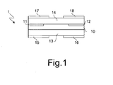
- the electroluminescent organic transistor 1 comprises at least one organic ambipolar semiconductor layer 10, which is suitable for the transport and the radiative recombination of charges of a first type, for example electrons, and of a second type, for example holes.
- a source electrode 11 suitable for the injection of said charges of a first type, for example electrons
- a drain electrode 12 suitable for the injection of said charges of a second type, for example holes.
- the group formed by said organic ambipolar semiconductor layer 10 and said source electrodes 11 and drain 12 in contact with said layer 10 is arranged between two layers of dielectric material 13 and 14.
- the electroluminescent organic transistor 1 also comprises a first control electrode 15 and a second control electrode 16, so that said first layer of dielectric material 13 is disposed between said layer of organic semiconductor 10 and said first and second control electrodes 15 and 16.
- the electroluminescent organic transistor 1 further comprises a third control electrode 17 and a fourth control electrode 18, so that said second layer of dielectric material 14 is disposed between said layer of organic semiconductor 10 and said third and fourth control electrodes 17 and 18.
- the source electrode 11 and the drain electrode 12 are respectively positioned defining a plane that is parallel with respect to the organic ambipolar semiconductor layer 10 (i.e. defining a plane that is perpendicular with respect to the stacking direction of the multilayer structure of the final device), in order to allow the exploitation of the field effect charge transport in correspondence of the interfaces between the organic ambipolar semiconductor layer 10 and the dielectric layers 13 and 14.
- said source electrode 11 and said drain electrode 12 are on the same side of the organic semiconductor layer 10, and in other words they are both in contact with said first layer of dielectric material 13 or with said second layer of dielectric material 14.
- These source and drain electrodes 11 and 12 may be arranged over a substantially flat surface of said layer of semiconductor material 10. Alternatively, these source and drain electrodes 11 and 12 may be each arranged in a suitable recess of said layer of semiconductor material 10.
- such electrodes may be embedded within the organic semiconductor material 10, or may have the same thickness of this layer of semiconductor material 10 and be "capping" the sides of said layer.
- said source electrode 11 and said drain electrode 12 are coplanar with said layer of semiconductor material 10, or said electrodes 11 and 12 both lie on a plane parallel to a plane on which said layer of semiconductor material 10 lies.
- Said organic semiconductor layer 10 may be made of any suitable material known as suitable for the ambipolar transport of charges in electroluminescent organic devices.
- suitable for use within the structures described by the present invention are oligoacenes, oligothiophenes, oligofluorenes, pyrimidine derivatives of oligothiophenes, carbonyl derivatives of oligothiophenes, ⁇ - and ⁇ - asymmetrically substituted tetrathiophenes with alkyl chains and perfluorinated chains, oligothiophenes with thiazole core, copolymers of polyfluorene, derivatives of poly (p-phenylene-vinylene), derivatives of Poly (9,9-dioctylfluorene), derivatives of poly (9,9-dioctylfluorene-benzothiadiazole).
- the one forming the semiconductor layer can be selected among the carbonyl derivatives of oligothiophen
- the thickness of the semiconductor layer in the solution described by the present invention must be between 10 nm and 150 nm. In its particularly preferred embodiment, said thickness is between 40 nm and 100nm.
- ITO Indium tin oxide
- gold gold, copper, silver, aluminum, calcium, magnesium, chromium, iron and poly (3,4-ethylenedioxythiophene) combined with poly (styrenesulfonate) (PEDOT: PSS)
- PEDOT poly (styrenesulfonate)
- the selection may be made among aluminum, calcium, magnesium, or gold.
- ITO indium tin oxide
- gold gold, copper, silver, aluminum, calcium, magnesium, chromium, iron and poly (3,4-ethylenedioxythiophene) combined with poly (styrenesulfonate) (PEDOT: PSS).
- PEDOT poly (styrenesulfonate)
- ITO gold or indium tin oxide (ITO) can be used for this purpose.
- the materials of the first dielectric layer 13 and the second dielectric layer 14 may be chosen from among the conventional dielectric materials for electroluminescent organic transistors.
- silicon dioxide, polymethylmethacrylate (PMMA), zinc oxide, alumina, zirconium dioxide, hafnium dioxide, fluoropolymers, such as for example the commercial product CytopTM, polyvinyl alcohol (PVA) and polystyrene (PS) can be used.
- said layer 13 comprises two layers of zirconium dioxide and polymethyl methacrylate and said layer 14 consists of polymethylmethacrylate or CytopTM.
- the thickness of said dielectric layers depends on the specific material selected: purely by way of example, said layer 13, in the case it is made of zirconium dioxide and polymethylmethacrylate, the layer of zirconium dioxide has a thickness between 100 and 250 nm, while the layer of polymethylmethacrylate has a thickness between 50 and 200 nm; for said layer 14 the layer of pol ymethylmethacryl ate or CytopTM has a thickness between 350 and 500 nm.
- the materials of the first control electrode 15 and the second control electrode 16 may be selected from indium tin oxide (ITO), gold, copper, silver, aluminum. In particular, indium tin oxide and/or gold may be preferably used.
- the materials of the third control electrode 17 and the fourth control electrode 18 may be selected from indium tin oxide (ITO), gold, copper, silver, aluminum. In particular, indium tin oxide and/or gold may be preferably used.
Landscapes
- Physics & Mathematics (AREA)
- Optics & Photonics (AREA)
- Electroluminescent Light Sources (AREA)
- Thin Film Transistor (AREA)
Description
- The present invention relates to an electroluminescent organic transistor.
- In the organic electronics field Organic Light Emitting Diodes (OLEDs) have been widely studied and many structural embodiments have been developed in order to obtain devices based on them.
- The application
JP2003100457 JP2003100457 - The scientific publication entitled "Materials for high performance single layer OLED device" by Huang et. A. published in Significant Research Achievements of Academia Sinica vol. 96 (2007) pages 13-16 discloses the possibility to substitute tri-layer semiconductor structures with a single bipolar layer, but is silent on how to overcome the performance limitations of the structures of
JP2003100457 - It is known from
US2009/0212281 an organic semiconductor transistor comprising an ambipolar organic semiconductor layer for the transport of electrons and holes, an electrode for the injection of the holes in the semiconductor layer, an electrode for injecting electrons in the semiconductor layer which is located at a certain distance from the first electrode, and two control electrodes separated from the organic semiconductor layer by means of an insulating layer. Of said control electrodes, one is opposed to a region of the organic semiconductor layer near the electrode for the injection of electrons and the other is opposed to the region of the organic semiconductor layer near the electrode for injection of the holes. - In the device disclosed in
US2009/0212281 , charge accumulation, charge transport and charge radiative recombination occur in correspondence of a single interface of the ambipolar organic semiconductor, in particular they occur at the interface between the organic semiconductor layer and the dielectric layer. This inherent feature of the known device causes the thickness of the semiconductor layer in which light is formed to be limited to a few molecular layers, thereby limiting the intensity of the light generated by the device. - Moreover, the intrinsic characteristics of the known device cause significant quenching phenomena of excitons, which are due to the interaction between said excitons and the free charges in the transistor channel, with a consequent limitation of the brightness and efficiency of the device.
- It is known from application
WO2010/049871 a field effect transistor comprising two dielectric layers, two control electrodes or gates, and an assembly consisting of a source electrode or source, a drain electrode or drain, and an organic semiconductor in contact with said source and drain. Such an assembly is arranged between said two dielectric layers, each of which is arranged between said assembly and a control electrode. A light emitting transistor comprising such a transistor is disclosed, wherein said organic semiconductor is an electroluminescent semiconductor organic layer with ambipolar properties. - In the light emitting transistor according to application
WO2010/049871 , charge transport takes place on both the interfaces between the organic semiconductor layer and the first dielectric layer and between the organic semiconductor layer and the second dielectric layer. Practically, these two interfaces have very different charge transport properties, since the molecular order of the semiconductor layer in correspondence of the two interfaces is very different. - The presence of only two control electrodes, one above and one below the semiconductor layer, limits the possibility of control of charge balancing in this device, that is an essential factor to obtain high brightness and efficiency of light emission.
- The objective of the present invention is therefore to provide an electroluminescent organic transistor which is improved with respect to the drawbacks of the prior art. Said objective is achieved with an electroluminescent organic transistor whose main features are specified in the first claim, while other features are specified in the remaining claims.
- A first advantage of the electroluminescent organic transistor according to the present invention consists in the fact that it allows the generation of a transversal electric field with respect to the plane of the organic semiconductor layer, with radiative recombination of the charges and generation of excitons through the entire thickness of the organic semiconductor layer. Consequently, attenuation of the quenching phenomenon of the excitons is achieved, wherein said phenomenon, present in all devices having a single semiconductor layer, is due to interaction with the free charges and derives from the spatial overlap between the charges accumulated at the interface between the organic semiconductor and the dielectric layers and the excitons generated near the same interface.
- A further advantage of the electroluminescent organic transistor according to the present invention consists in the fact that it allows to maximize the current density in the organic semiconductor layer, the accumulation of charge and, consequently, it allows to maximize the light intensity.
- Finally, the organic transistor according to the present invention allows an optimization of the charge balancing in the device. In fact, thanks to the presence of two control electrodes on each side of the device, it allows to effectively exploit the charge transport on both interfaces of the organic semiconductor layer and to balance the differences in the mobility of the charges in the organic semiconductor layer by an appropriate modulation of the potentials of the control electrodes.
- Further advantages and features of the device according to the present invention will become apparent to those skilled in the art from the following detailed and nonlimiting description of an embodiment thereof with reference to the accompanying drawing in which:
-
Figure 1 shows a schematic sectional view of an electroluminescent organic transistor according to the present invention. - The features of the drawing are not to scale, but their dimensions are enlarged or reduced in order to increase the clarity of the drawing.
- Referring to
Figure 1 , it is shown that the electroluminescent organic transistor 1 according to the present invention comprises at least one organicambipolar semiconductor layer 10, which is suitable for the transport and the radiative recombination of charges of a first type, for example electrons, and of a second type, for example holes. - In contact with said organic
ambipolar semiconductor layer 10 , are arranged asource electrode 11, suitable for the injection of said charges of a first type, for example electrons, and adrain electrode 12, suitable for the injection of said charges of a second type, for example holes. - The group formed by said organic
ambipolar semiconductor layer 10 and saidsource electrodes 11 anddrain 12 in contact with saidlayer 10 is arranged between two layers ofdielectric material - The electroluminescent organic transistor 1 according to the present invention also comprises a
first control electrode 15 and asecond control electrode 16, so that said first layer ofdielectric material 13 is disposed between said layer oforganic semiconductor 10 and said first andsecond control electrodes - The electroluminescent organic transistor 1 according to the present invention further comprises a
third control electrode 17 and afourth control electrode 18, so that said second layer ofdielectric material 14 is disposed between said layer oforganic semiconductor 10 and said third andfourth control electrodes - The
source electrode 11 and thedrain electrode 12 are respectively positioned defining a plane that is parallel with respect to the organic ambipolar semiconductor layer 10 (i.e. defining a plane that is perpendicular with respect to the stacking direction of the multilayer structure of the final device), in order to allow the exploitation of the field effect charge transport in correspondence of the interfaces between the organicambipolar semiconductor layer 10 and thedielectric layers - According to an embodiment of the invention, said
source electrode 11 and saiddrain electrode 12 are on the same side of theorganic semiconductor layer 10, and in other words they are both in contact with said first layer ofdielectric material 13 or with said second layer ofdielectric material 14. - These source and
drain electrodes semiconductor material 10. Alternatively, these source anddrain electrodes semiconductor material 10. - In other embodiments of the invention such electrodes may be embedded within the
organic semiconductor material 10, or may have the same thickness of this layer ofsemiconductor material 10 and be "capping" the sides of said layer. - Preferably, in the electroluminescent organic transistor according to the present invention, said
source electrode 11 and saiddrain electrode 12 are coplanar with said layer ofsemiconductor material 10, or saidelectrodes semiconductor material 10 lies. - Said
organic semiconductor layer 10 may be made of any suitable material known as suitable for the ambipolar transport of charges in electroluminescent organic devices. For example suitable for use within the structures described by the present invention are oligoacenes, oligothiophenes, oligofluorenes, pyrimidine derivatives of oligothiophenes, carbonyl derivatives of oligothiophenes, α- and ω- asymmetrically substituted tetrathiophenes with alkyl chains and perfluorinated chains, oligothiophenes with thiazole core, copolymers of polyfluorene, derivatives of poly (p-phenylene-vinylene), derivatives of Poly (9,9-dioctylfluorene), derivatives of poly (9,9-dioctylfluorene-benzothiadiazole). Preferably among said materials, the one forming the semiconductor layer can be selected among the carbonyl derivatives of oligothiophenes, derivatives of fluorene and derivatives of poly (p-phenylene-vinylene). - The thickness of the semiconductor layer in the solution described by the present invention must be between 10 nm and 150 nm. In its particularly preferred embodiment, said thickness is between 40 nm and 100nm.
- Indium tin oxide (ITO), gold, copper, silver, aluminum, calcium, magnesium, chromium, iron and poly (3,4-ethylenedioxythiophene) combined with poly (styrenesulfonate) (PEDOT: PSS) can be used as a material for said
source electrode 11. Preferably, the selection may be made among aluminum, calcium, magnesium, or gold. - As a material for said
drain electrode 12, indium tin oxide (ITO), gold, copper, silver, aluminum, calcium, magnesium, chromium, iron and poly (3,4-ethylenedioxythiophene) combined with poly (styrenesulfonate) (PEDOT: PSS). In a particularly preferred embodiment, gold or indium tin oxide (ITO) can be used for this purpose. - The materials of the first
dielectric layer 13 and the seconddielectric layer 14 may be chosen from among the conventional dielectric materials for electroluminescent organic transistors. In particular, silicon dioxide, polymethylmethacrylate (PMMA), zinc oxide, alumina, zirconium dioxide, hafnium dioxide, fluoropolymers, such as for example the commercial product Cytop™, polyvinyl alcohol (PVA) and polystyrene (PS) can be used. Preferably, saidlayer 13 comprises two layers of zirconium dioxide and polymethyl methacrylate and saidlayer 14 consists of polymethylmethacrylate or Cytop™. Generally, the thickness of said dielectric layers depends on the specific material selected: purely by way of example, saidlayer 13, in the case it is made of zirconium dioxide and polymethylmethacrylate, the layer of zirconium dioxide has a thickness between 100 and 250 nm, while the layer of polymethylmethacrylate has a thickness between 50 and 200 nm; for saidlayer 14 the layer of pol ymethylmethacryl ate or Cytop™ has a thickness between 350 and 500 nm. - The materials of the
first control electrode 15 and thesecond control electrode 16 may be selected from indium tin oxide (ITO), gold, copper, silver, aluminum. In particular, indium tin oxide and/or gold may be preferably used. - The materials of the
third control electrode 17 and thefourth control electrode 18 may be selected from indium tin oxide (ITO), gold, copper, silver, aluminum. In particular, indium tin oxide and/or gold may be preferably used. - Possible modifications and/or additions may be made by those skilled in the art to the hereinabove disclosed and illustrated embodiment while remaining within the scope of the following claims.
Claims (9)
- An electroluminescent organic transistor (1), comprising:- at least one layer of an ambipolar organic semiconductor (10) suitable for transport and radiative recombination of charges of a first type and of a second type;- a source electrode (11) suitable for injection of said charges of a first type;- a drain electrode (12) suitable for injection of said charges of a second type;- said source electrode (11) and said drain electrode (12) being in contact with said layer of ambipolar organic semiconductor (10);- a first (15) and a second control electrode (16).- a first layer of a dielectric material (13) positioned between said layer of ambipolar organic semiconductor (10) and said first (15) and second (16) control electrode;- a third (17) and a fourth control electrode (18); and- a second layer of a dielectric material (14) positioned between said layer of ambipolar organic semiconductor (10) and said third (17) and fourth (18) control electrode; characterized in that both said source electrode (11) and said drain electrode (12) lie on a plane that is parallel to a plane on which said layer of ambipolar organic semiconductor (10) lies.
- An electroluminescent organic transistor according to the previous claim, characterized in that said source electrode (11) and said drain electrode (12) are both in contact with said first layer of dielectric material (13) or with said second layer of dielectric material (14).
- An electroluminescent organic transistor according to claim 1, characterized in that the thickness of said layer of ambipolar organic semiconductor (10) is between 10 and 150 nm.
- An electroluminescent organic transistor according to claim 3, characterized in that the thickness of said layer of ambipolar organic semiconductor (10) is between 40 and 100 nm.
- An electroluminescent organic transistor according to claim 1, characterized in that said ambipolar organic semiconductor (10) is selected in the group consisting of oligoacenes, oligothiophenes, oligofluorenes, pyrimidine derivatives of oligothiophenes, carbonyl derivatives of oligothiophenes, tetrathiophenes asymmetrically substituted in α and ω positions with alkyl and perfluorinated chains, oligothiophenes with thiazole core, polyfluorene copolymers, poly(p-phenylene-vinylene) derivatives, poly(9,9-dioctylfluorene) derivatives and poly(9,9-dioctylfluorene-benzothiadiazole) derivatives.
- An electroluminescent organic transistor according to claim 5, characterized in that said ambipolar organic semiconductor (10) is selected in the group consisting of carbonyl derivatives of oligothiophenes, fluorene derivatives and poly(p-phenylene-vinylene) derivatives.
- An electroluminescent organic transistor according to claim 1, characterized in that said drain (12) and source (11) electrodes are formed of a material selected in the group consisting of indium and tin oxide (ITO), gold, copper, silver, aluminum, calcium, magnesium, chromium, iron and poly(3,4-ethylenedioxythiophene) combined with poly(styrenesulfonate) (PEDOT:PSS).
- An electroluminescent organic transistor according to claim 1, characterized in that said control electrodes (15-18) are formed of at least one material selected in the group consisting of indium and tin oxide (ITO), gold, copper, silver and aluminum.
- An electroluminescent organic transistor according to claim 1, characterized in that said first (13) and second (14) layer of dielectric material are formed of a material selected in the group consisting of silicon dioxide, polymethylmethacrylate (PMMA), zinc oxide, alumina, zirconium dioxide, hafnium dioxide, fluoropolymers, polyvinyl alcohol (PVA) and polystyrene (PS).
Applications Claiming Priority (2)
| Application Number | Priority Date | Filing Date | Title |
|---|---|---|---|
| IT001446A ITMI20111446A1 (en) | 2011-07-29 | 2011-07-29 | ELECTROLUMINESCENT ORGANIC TRANSISTOR |
| PCT/IB2012/053817 WO2013018002A1 (en) | 2011-07-29 | 2012-07-26 | Electroluminescent organic transistor |
Publications (2)
| Publication Number | Publication Date |
|---|---|
| EP2574219A1 EP2574219A1 (en) | 2013-04-03 |
| EP2574219B1 true EP2574219B1 (en) | 2014-04-02 |
Family
ID=44584355
Family Applications (1)
| Application Number | Title | Priority Date | Filing Date |
|---|---|---|---|
| EP12759237.6A Not-in-force EP2574219B1 (en) | 2011-07-29 | 2012-07-26 | Electroluminescent organic transistor |
Country Status (7)
| Country | Link |
|---|---|
| US (1) | US8729540B2 (en) |
| EP (1) | EP2574219B1 (en) |
| JP (1) | JP5678236B2 (en) |
| KR (1) | KR101570407B1 (en) |
| CN (1) | CN103718327B (en) |
| IT (1) | ITMI20111446A1 (en) |
| WO (1) | WO2013018002A1 (en) |
Families Citing this family (10)
| Publication number | Priority date | Publication date | Assignee | Title |
|---|---|---|---|---|
| ITMI20111445A1 (en) * | 2011-07-29 | 2013-01-30 | E T C Srl | ELECTROLUMINESCENT ORGANIC TRANSISTOR DOUBLE GATE |
| EP2858116A1 (en) * | 2013-10-01 | 2015-04-08 | Nederlandse Organisatie voor toegepast -natuurwetenschappelijk onderzoek TNO | Ambipolar transistor device and method of operating the device |
| EP2960280A1 (en) | 2014-06-26 | 2015-12-30 | E.T.C. S.r.l. | Photocrosslinkable compositions, patterned high k thin film dielectrics and related devices |
| EP2978035A1 (en) | 2014-07-24 | 2016-01-27 | E.T.C. S.r.l. | Organic electroluminescent transistor |
| EP2978037A1 (en) | 2014-07-24 | 2016-01-27 | E.T.C. S.r.l. | Organic electroluminescent transistor |
| EP2978038A1 (en) | 2014-07-24 | 2016-01-27 | E.T.C. S.r.l. | Organic electroluminescent transistor |
| CN111146352B (en) | 2014-07-24 | 2022-10-21 | 飞利斯有限公司 | Organic electroluminescent transistor |
| EP3021373A1 (en) | 2014-11-14 | 2016-05-18 | E.T.C. S.r.l. | Display containing improved pixel architectures |
| WO2016100983A1 (en) | 2014-12-19 | 2016-06-23 | Polyera Corporation | Photocrosslinkable compositions, patterned high k thin film dielectrics and related devices |
| CN105679940A (en) * | 2016-04-19 | 2016-06-15 | 中国科学院化学研究所 | Bipolar polymer field effect transistor and preparation method and application thereof |
Family Cites Families (14)
| Publication number | Priority date | Publication date | Assignee | Title |
|---|---|---|---|---|
| US6720572B1 (en) | 1999-06-25 | 2004-04-13 | The Penn State Research Foundation | Organic light emitters with improved carrier injection |
| JP2003100457A (en) * | 2001-09-21 | 2003-04-04 | Seiko Epson Corp | Light emitting device |
| JP4246949B2 (en) * | 2002-03-25 | 2009-04-02 | 株式会社半導体エネルギー研究所 | Organic thin film light emitting transistor |
| EP1367659B1 (en) | 2002-05-21 | 2012-09-05 | Semiconductor Energy Laboratory Co., Ltd. | Organic field effect transistor |
| JP2004128469A (en) * | 2002-07-31 | 2004-04-22 | Mitsubishi Chemicals Corp | Field effect transistor |
| US7511421B2 (en) * | 2003-08-25 | 2009-03-31 | Semiconductor Energy Laboratory Co., Ltd. | Mixed metal and organic electrode for organic device |
| DE602004006441T2 (en) * | 2003-12-22 | 2008-05-15 | Koninklijke Philips Electronics N.V. | NON-VOLATILE FERROELECTRIC THIN FILM COMPONENT WITH AN ORGANIC AMBIPOLAR SEMICONDUCTOR AND METHOD FOR PROCESSING SUCH A COMPONENT |
| JP4530334B2 (en) * | 2004-01-21 | 2010-08-25 | 国立大学法人京都大学 | ORGANIC SEMICONDUCTOR DEVICE AND DISPLAY DEVICE AND IMAGING DEVICE USING THE SAME |
| US7494722B2 (en) | 2005-02-23 | 2009-02-24 | Eastman Kodak Company | Tandem OLED having an organic intermediate connector |
| JP2007109564A (en) | 2005-10-14 | 2007-04-26 | Pioneer Electronic Corp | Light emitting element and display device |
| US8026512B2 (en) | 2006-11-16 | 2011-09-27 | Panasonic Corporation | Mobility engineered electroluminescent devices |
| JP5403518B2 (en) * | 2008-02-08 | 2014-01-29 | 国立大学法人京都工芸繊維大学 | Driving method and driving apparatus for light emitting device |
| CN102203974A (en) * | 2008-10-29 | 2011-09-28 | 皇家飞利浦电子股份有限公司 | Dual gate field-effect transistor and method of producing a dual gate field-effect transistor |
| JP5447794B2 (en) * | 2009-05-08 | 2014-03-19 | セイコーエプソン株式会社 | Light emitting device |
-
2011
- 2011-07-29 IT IT001446A patent/ITMI20111446A1/en unknown
-
2012
- 2012-07-26 EP EP12759237.6A patent/EP2574219B1/en not_active Not-in-force
- 2012-07-26 KR KR1020147005651A patent/KR101570407B1/en not_active Expired - Fee Related
- 2012-07-26 CN CN201280038021.1A patent/CN103718327B/en not_active Expired - Fee Related
- 2012-07-26 JP JP2014522203A patent/JP5678236B2/en not_active Expired - Fee Related
- 2012-07-26 WO PCT/IB2012/053817 patent/WO2013018002A1/en not_active Ceased
- 2012-07-26 US US13/806,898 patent/US8729540B2/en active Active
Also Published As
| Publication number | Publication date |
|---|---|
| JP5678236B2 (en) | 2015-02-25 |
| KR101570407B1 (en) | 2015-11-20 |
| US8729540B2 (en) | 2014-05-20 |
| WO2013018002A1 (en) | 2013-02-07 |
| CN103718327A (en) | 2014-04-09 |
| CN103718327B (en) | 2016-04-06 |
| EP2574219A1 (en) | 2013-04-03 |
| ITMI20111446A1 (en) | 2013-01-30 |
| KR20140065403A (en) | 2014-05-29 |
| US20130320311A1 (en) | 2013-12-05 |
| JP2014525149A (en) | 2014-09-25 |
Similar Documents
| Publication | Publication Date | Title |
|---|---|---|
| US8729540B2 (en) | Electroluminescent organic transistor | |
| Wang et al. | Advances in alternating current electroluminescent devices | |
| EP2583329B1 (en) | Electroluminescent organic transistor | |
| EP2737559B1 (en) | Electroluminescent organic double gate transistor | |
| Chen et al. | Recent Advances in Multi‐Layer Light‐Emitting Heterostructure Transistors | |
| CN103956433A (en) | Monopole organic light-emitting field effect transistor | |
| KR101339549B1 (en) | Organic light emitting diode and a fabrication method thereof | |
| JP2014525149A5 (en) | ||
| WO2013122198A1 (en) | Organic light-emitting transistor having second gate electrode | |
| CN103325815B (en) | Organic light emitting device and method of manufacturing organic light emitting device | |
| CN103972390B (en) | Bipolar type organic light-emitting field effect transistor | |
| KR101730902B1 (en) | Vertical-type organic light-emitting transistors with reduced leakage current and method for fabricating the same | |
| DE102014110054A1 (en) | Optoelectronic assembly and method for manufacturing an optoelectronic assembly | |
| TW201900847A (en) | Organic electroluminescent device | |
| US9343707B2 (en) | Electroluminescent organic double gate transistor | |
| KR20160024091A (en) | Organic light emitting display apparatus | |
| CN1960023A (en) | Organic electroluminescent element and electron transport layer |
Legal Events
| Date | Code | Title | Description |
|---|---|---|---|
| PUAI | Public reference made under article 153(3) epc to a published international application that has entered the european phase |
Free format text: ORIGINAL CODE: 0009012 |
|
| 17P | Request for examination filed |
Effective date: 20121231 |
|
| AK | Designated contracting states |
Kind code of ref document: A1 Designated state(s): AL AT BE BG CH CY CZ DE DK EE ES FI FR GB GR HR HU IE IS IT LI LT LU LV MC MK MT NL NO PL PT RO RS SE SI SK SM TR |
|
| GRAP | Despatch of communication of intention to grant a patent |
Free format text: ORIGINAL CODE: EPIDOSNIGR1 |
|
| INTG | Intention to grant announced |
Effective date: 20131128 |
|
| RIN1 | Information on inventor provided before grant (corrected) |
Inventor name: MUCCINI, MICHELE Inventor name: TOFFANIN, STEFANO Inventor name: CAPELLI, RAFFAELLA |
|
| GRAS | Grant fee paid |
Free format text: ORIGINAL CODE: EPIDOSNIGR3 |
|
| GRAA | (expected) grant |
Free format text: ORIGINAL CODE: 0009210 |
|
| AK | Designated contracting states |
Kind code of ref document: B1 Designated state(s): AL AT BE BG CH CY CZ DE DK EE ES FI FR GB GR HR HU IE IS IT LI LT LU LV MC MK MT NL NO PL PT RO RS SE SI SK SM TR |
|
| DAX | Request for extension of the european patent (deleted) | ||
| REG | Reference to a national code |
Ref country code: GB Ref legal event code: FG4D |
|
| REG | Reference to a national code |
Ref country code: AT Ref legal event code: REF Ref document number: 660605 Country of ref document: AT Kind code of ref document: T Effective date: 20140415 Ref country code: CH Ref legal event code: EP |
|
| REG | Reference to a national code |
Ref country code: IE Ref legal event code: FG4D |
|
| REG | Reference to a national code |
Ref country code: DE Ref legal event code: R096 Ref document number: 602012001308 Country of ref document: DE Effective date: 20140515 |
|
| REG | Reference to a national code |
Ref country code: NL Ref legal event code: T3 |
|
| REG | Reference to a national code |
Ref country code: AT Ref legal event code: MK05 Ref document number: 660605 Country of ref document: AT Kind code of ref document: T Effective date: 20140402 |
|
| REG | Reference to a national code |
Ref country code: LT Ref legal event code: MG4D |
|
| PG25 | Lapsed in a contracting state [announced via postgrant information from national office to epo] |
Ref country code: CZ Free format text: LAPSE BECAUSE OF FAILURE TO SUBMIT A TRANSLATION OF THE DESCRIPTION OR TO PAY THE FEE WITHIN THE PRESCRIBED TIME-LIMIT Effective date: 20140402 Ref country code: NO Free format text: LAPSE BECAUSE OF FAILURE TO SUBMIT A TRANSLATION OF THE DESCRIPTION OR TO PAY THE FEE WITHIN THE PRESCRIBED TIME-LIMIT Effective date: 20140702 Ref country code: LT Free format text: LAPSE BECAUSE OF FAILURE TO SUBMIT A TRANSLATION OF THE DESCRIPTION OR TO PAY THE FEE WITHIN THE PRESCRIBED TIME-LIMIT Effective date: 20140402 Ref country code: CY Free format text: LAPSE BECAUSE OF FAILURE TO SUBMIT A TRANSLATION OF THE DESCRIPTION OR TO PAY THE FEE WITHIN THE PRESCRIBED TIME-LIMIT Effective date: 20140402 Ref country code: FI Free format text: LAPSE BECAUSE OF FAILURE TO SUBMIT A TRANSLATION OF THE DESCRIPTION OR TO PAY THE FEE WITHIN THE PRESCRIBED TIME-LIMIT Effective date: 20140402 Ref country code: GR Free format text: LAPSE BECAUSE OF FAILURE TO SUBMIT A TRANSLATION OF THE DESCRIPTION OR TO PAY THE FEE WITHIN THE PRESCRIBED TIME-LIMIT Effective date: 20140703 Ref country code: IS Free format text: LAPSE BECAUSE OF FAILURE TO SUBMIT A TRANSLATION OF THE DESCRIPTION OR TO PAY THE FEE WITHIN THE PRESCRIBED TIME-LIMIT Effective date: 20140802 Ref country code: BG Free format text: LAPSE BECAUSE OF FAILURE TO SUBMIT A TRANSLATION OF THE DESCRIPTION OR TO PAY THE FEE WITHIN THE PRESCRIBED TIME-LIMIT Effective date: 20140702 |
|
| PG25 | Lapsed in a contracting state [announced via postgrant information from national office to epo] |
Ref country code: RS Free format text: LAPSE BECAUSE OF FAILURE TO SUBMIT A TRANSLATION OF THE DESCRIPTION OR TO PAY THE FEE WITHIN THE PRESCRIBED TIME-LIMIT Effective date: 20140402 Ref country code: HR Free format text: LAPSE BECAUSE OF FAILURE TO SUBMIT A TRANSLATION OF THE DESCRIPTION OR TO PAY THE FEE WITHIN THE PRESCRIBED TIME-LIMIT Effective date: 20140402 Ref country code: PL Free format text: LAPSE BECAUSE OF FAILURE TO SUBMIT A TRANSLATION OF THE DESCRIPTION OR TO PAY THE FEE WITHIN THE PRESCRIBED TIME-LIMIT Effective date: 20140402 Ref country code: ES Free format text: LAPSE BECAUSE OF FAILURE TO SUBMIT A TRANSLATION OF THE DESCRIPTION OR TO PAY THE FEE WITHIN THE PRESCRIBED TIME-LIMIT Effective date: 20140402 Ref country code: AT Free format text: LAPSE BECAUSE OF FAILURE TO SUBMIT A TRANSLATION OF THE DESCRIPTION OR TO PAY THE FEE WITHIN THE PRESCRIBED TIME-LIMIT Effective date: 20140402 Ref country code: LV Free format text: LAPSE BECAUSE OF FAILURE TO SUBMIT A TRANSLATION OF THE DESCRIPTION OR TO PAY THE FEE WITHIN THE PRESCRIBED TIME-LIMIT Effective date: 20140402 Ref country code: SE Free format text: LAPSE BECAUSE OF FAILURE TO SUBMIT A TRANSLATION OF THE DESCRIPTION OR TO PAY THE FEE WITHIN THE PRESCRIBED TIME-LIMIT Effective date: 20140402 |
|
| PG25 | Lapsed in a contracting state [announced via postgrant information from national office to epo] |
Ref country code: PT Free format text: LAPSE BECAUSE OF FAILURE TO SUBMIT A TRANSLATION OF THE DESCRIPTION OR TO PAY THE FEE WITHIN THE PRESCRIBED TIME-LIMIT Effective date: 20140804 |
|
| REG | Reference to a national code |
Ref country code: DE Ref legal event code: R097 Ref document number: 602012001308 Country of ref document: DE |
|
| PG25 | Lapsed in a contracting state [announced via postgrant information from national office to epo] |
Ref country code: SK Free format text: LAPSE BECAUSE OF FAILURE TO SUBMIT A TRANSLATION OF THE DESCRIPTION OR TO PAY THE FEE WITHIN THE PRESCRIBED TIME-LIMIT Effective date: 20140402 Ref country code: RO Free format text: LAPSE BECAUSE OF FAILURE TO SUBMIT A TRANSLATION OF THE DESCRIPTION OR TO PAY THE FEE WITHIN THE PRESCRIBED TIME-LIMIT Effective date: 20140402 Ref country code: DK Free format text: LAPSE BECAUSE OF FAILURE TO SUBMIT A TRANSLATION OF THE DESCRIPTION OR TO PAY THE FEE WITHIN THE PRESCRIBED TIME-LIMIT Effective date: 20140402 Ref country code: EE Free format text: LAPSE BECAUSE OF FAILURE TO SUBMIT A TRANSLATION OF THE DESCRIPTION OR TO PAY THE FEE WITHIN THE PRESCRIBED TIME-LIMIT Effective date: 20140402 |
|
| PLBE | No opposition filed within time limit |
Free format text: ORIGINAL CODE: 0009261 |
|
| STAA | Information on the status of an ep patent application or granted ep patent |
Free format text: STATUS: NO OPPOSITION FILED WITHIN TIME LIMIT |
|
| PG25 | Lapsed in a contracting state [announced via postgrant information from national office to epo] |
Ref country code: LU Free format text: LAPSE BECAUSE OF FAILURE TO SUBMIT A TRANSLATION OF THE DESCRIPTION OR TO PAY THE FEE WITHIN THE PRESCRIBED TIME-LIMIT Effective date: 20140726 |
|
| 26N | No opposition filed |
Effective date: 20150106 |
|
| REG | Reference to a national code |
Ref country code: DE Ref legal event code: R097 Ref document number: 602012001308 Country of ref document: DE Effective date: 20150106 |
|
| REG | Reference to a national code |
Ref country code: IE Ref legal event code: MM4A |
|
| REG | Reference to a national code |
Ref country code: FR Ref legal event code: ST Effective date: 20150331 |
|
| PG25 | Lapsed in a contracting state [announced via postgrant information from national office to epo] |
Ref country code: FR Free format text: LAPSE BECAUSE OF NON-PAYMENT OF DUE FEES Effective date: 20140731 Ref country code: RS Free format text: LAPSE BECAUSE OF FAILURE TO SUBMIT A TRANSLATION OF THE DESCRIPTION OR TO PAY THE FEE WITHIN THE PRESCRIBED TIME-LIMIT Effective date: 20141119 |
|
| PG25 | Lapsed in a contracting state [announced via postgrant information from national office to epo] |
Ref country code: SI Free format text: LAPSE BECAUSE OF FAILURE TO SUBMIT A TRANSLATION OF THE DESCRIPTION OR TO PAY THE FEE WITHIN THE PRESCRIBED TIME-LIMIT Effective date: 20140402 |
|
| PG25 | Lapsed in a contracting state [announced via postgrant information from national office to epo] |
Ref country code: IE Free format text: LAPSE BECAUSE OF NON-PAYMENT OF DUE FEES Effective date: 20140726 |
|
| REG | Reference to a national code |
Ref country code: CH Ref legal event code: PL |
|
| PG25 | Lapsed in a contracting state [announced via postgrant information from national office to epo] |
Ref country code: MC Free format text: LAPSE BECAUSE OF FAILURE TO SUBMIT A TRANSLATION OF THE DESCRIPTION OR TO PAY THE FEE WITHIN THE PRESCRIBED TIME-LIMIT Effective date: 20140402 Ref country code: LI Free format text: LAPSE BECAUSE OF NON-PAYMENT OF DUE FEES Effective date: 20150731 Ref country code: CH Free format text: LAPSE BECAUSE OF NON-PAYMENT OF DUE FEES Effective date: 20150731 Ref country code: SM Free format text: LAPSE BECAUSE OF FAILURE TO SUBMIT A TRANSLATION OF THE DESCRIPTION OR TO PAY THE FEE WITHIN THE PRESCRIBED TIME-LIMIT Effective date: 20140402 |
|
| PG25 | Lapsed in a contracting state [announced via postgrant information from national office to epo] |
Ref country code: MT Free format text: LAPSE BECAUSE OF FAILURE TO SUBMIT A TRANSLATION OF THE DESCRIPTION OR TO PAY THE FEE WITHIN THE PRESCRIBED TIME-LIMIT Effective date: 20140402 |
|
| PG25 | Lapsed in a contracting state [announced via postgrant information from national office to epo] |
Ref country code: HU Free format text: LAPSE BECAUSE OF FAILURE TO SUBMIT A TRANSLATION OF THE DESCRIPTION OR TO PAY THE FEE WITHIN THE PRESCRIBED TIME-LIMIT; INVALID AB INITIO Effective date: 20120726 Ref country code: TR Free format text: LAPSE BECAUSE OF FAILURE TO SUBMIT A TRANSLATION OF THE DESCRIPTION OR TO PAY THE FEE WITHIN THE PRESCRIBED TIME-LIMIT Effective date: 20140402 |
|
| PG25 | Lapsed in a contracting state [announced via postgrant information from national office to epo] |
Ref country code: MK Free format text: LAPSE BECAUSE OF FAILURE TO SUBMIT A TRANSLATION OF THE DESCRIPTION OR TO PAY THE FEE WITHIN THE PRESCRIBED TIME-LIMIT Effective date: 20140402 |
|
| PG25 | Lapsed in a contracting state [announced via postgrant information from national office to epo] |
Ref country code: AL Free format text: LAPSE BECAUSE OF FAILURE TO SUBMIT A TRANSLATION OF THE DESCRIPTION OR TO PAY THE FEE WITHIN THE PRESCRIBED TIME-LIMIT Effective date: 20140402 |
|
| REG | Reference to a national code |
Ref country code: DE Ref legal event code: R082 Ref document number: 602012001308 Country of ref document: DE Representative=s name: COHAUSZ & FLORACK PATENT- UND RECHTSANWAELTE P, DE Ref country code: DE Ref legal event code: R081 Ref document number: 602012001308 Country of ref document: DE Owner name: FLEXTERRA, INC., SKOKIE, US Free format text: FORMER OWNER: E.T.C. S.R.L., BOLOGNA, IT |
|
| REG | Reference to a national code |
Ref country code: GB Ref legal event code: 732E Free format text: REGISTERED BETWEEN 20190503 AND 20190508 |
|
| REG | Reference to a national code |
Ref country code: NL Ref legal event code: HC Owner name: E.T.C. S.R.L. IN LIQUIDAZIONE; IT Free format text: DETAILS ASSIGNMENT: CHANGE OF OWNER(S), CHANGE OF OWNER(S) NAME; FORMER OWNER NAME: E.T.C. S.R.L. Effective date: 20190411 Ref country code: NL Ref legal event code: PD Owner name: FLEXTERRA, INC.; US Free format text: DETAILS ASSIGNMENT: CHANGE OF OWNER(S), ASSIGNMENT; FORMER OWNER NAME: E.T.C. S.R.L. IN LIQUIDAZIONE Effective date: 20190411 |
|
| REG | Reference to a national code |
Ref country code: BE Ref legal event code: HC Owner name: E.T.C. S.R.L. UNDER LIQUIDATION; IT Free format text: DETAILS ASSIGNMENT: CHANGE OF OWNER(S), CHANGEMENT DE NOM DU PROPRIETAIRE; FORMER OWNER NAME: E.T.C. S.R.L. Effective date: 20190411 Ref country code: BE Ref legal event code: PD Owner name: FLEXTERRA, INC.; US Free format text: DETAILS ASSIGNMENT: CHANGE OF OWNER(S), CESSION; FORMER OWNER NAME: E.T.C. S.R.L. UNDER LIQUIDATION Effective date: 20190411 |
|
| REG | Reference to a national code |
Ref country code: DE Ref legal event code: R079 Ref document number: 602012001308 Country of ref document: DE Free format text: PREVIOUS MAIN CLASS: H01L0051520000 Ipc: H10K0050800000 |
|
| P01 | Opt-out of the competence of the unified patent court (upc) registered |
Effective date: 20230521 |
|
| PGFP | Annual fee paid to national office [announced via postgrant information from national office to epo] |
Ref country code: NL Payment date: 20230726 Year of fee payment: 12 |
|
| PGFP | Annual fee paid to national office [announced via postgrant information from national office to epo] |
Ref country code: IT Payment date: 20230720 Year of fee payment: 12 Ref country code: GB Payment date: 20230727 Year of fee payment: 12 |
|
| PGFP | Annual fee paid to national office [announced via postgrant information from national office to epo] |
Ref country code: DE Payment date: 20230727 Year of fee payment: 12 Ref country code: BE Payment date: 20230727 Year of fee payment: 12 |
|
| REG | Reference to a national code |
Ref country code: DE Ref legal event code: R119 Ref document number: 602012001308 Country of ref document: DE |
|
| REG | Reference to a national code |
Ref country code: NL Ref legal event code: MM Effective date: 20240801 |
|
| GBPC | Gb: european patent ceased through non-payment of renewal fee |
Effective date: 20240726 |
|
| PG25 | Lapsed in a contracting state [announced via postgrant information from national office to epo] |
Ref country code: DE Free format text: LAPSE BECAUSE OF NON-PAYMENT OF DUE FEES Effective date: 20250201 |
|
| PG25 | Lapsed in a contracting state [announced via postgrant information from national office to epo] |
Ref country code: NL Free format text: LAPSE BECAUSE OF NON-PAYMENT OF DUE FEES Effective date: 20240801 |
|
| PG25 | Lapsed in a contracting state [announced via postgrant information from national office to epo] |
Ref country code: BE Free format text: LAPSE BECAUSE OF NON-PAYMENT OF DUE FEES Effective date: 20240731 |
|
| PG25 | Lapsed in a contracting state [announced via postgrant information from national office to epo] |
Ref country code: GB Free format text: LAPSE BECAUSE OF NON-PAYMENT OF DUE FEES Effective date: 20240726 |
|
| REG | Reference to a national code |
Ref country code: BE Ref legal event code: MM Effective date: 20240731 |
|
| PG25 | Lapsed in a contracting state [announced via postgrant information from national office to epo] |
Ref country code: IT Free format text: LAPSE BECAUSE OF NON-PAYMENT OF DUE FEES Effective date: 20240726 |