JP5447794B2 - Light emitting device - Google Patents
Light emitting device Download PDFInfo
- Publication number
- JP5447794B2 JP5447794B2 JP2009113492A JP2009113492A JP5447794B2 JP 5447794 B2 JP5447794 B2 JP 5447794B2 JP 2009113492 A JP2009113492 A JP 2009113492A JP 2009113492 A JP2009113492 A JP 2009113492A JP 5447794 B2 JP5447794 B2 JP 5447794B2
- Authority
- JP
- Japan
- Prior art keywords
- light
- layer
- electrode
- light receiving
- cladding layer
- Prior art date
- Legal status (The legal status is an assumption and is not a legal conclusion. Google has not performed a legal analysis and makes no representation as to the accuracy of the status listed.)
- Expired - Fee Related
Links
- 238000005253 cladding Methods 0.000 claims description 64
- 239000000758 substrate Substances 0.000 claims description 30
- 230000031700 light absorption Effects 0.000 claims description 26
- 238000000926 separation method Methods 0.000 claims description 12
- 239000010410 layer Substances 0.000 description 216
- 230000004048 modification Effects 0.000 description 25
- 238000012986 modification Methods 0.000 description 25
- 238000004519 manufacturing process Methods 0.000 description 12
- 238000000034 method Methods 0.000 description 10
- 239000004065 semiconductor Substances 0.000 description 9
- 229910001218 Gallium arsenide Inorganic materials 0.000 description 8
- 239000000463 material Substances 0.000 description 6
- 230000003287 optical effect Effects 0.000 description 6
- 229910000980 Aluminium gallium arsenide Inorganic materials 0.000 description 5
- 238000001514 detection method Methods 0.000 description 4
- 230000010355 oscillation Effects 0.000 description 4
- 239000012535 impurity Substances 0.000 description 3
- 229910004298 SiO 2 Inorganic materials 0.000 description 2
- 238000001451 molecular beam epitaxy Methods 0.000 description 2
- 230000006798 recombination Effects 0.000 description 2
- 238000005215 recombination Methods 0.000 description 2
- 238000001771 vacuum deposition Methods 0.000 description 2
- 229910018072 Al 2 O 3 Inorganic materials 0.000 description 1
- 229910002704 AlGaN Inorganic materials 0.000 description 1
- 229910000530 Gallium indium arsenide Inorganic materials 0.000 description 1
- -1 InGaN Inorganic materials 0.000 description 1
- 239000004642 Polyimide Substances 0.000 description 1
- 230000004888 barrier function Effects 0.000 description 1
- 239000000969 carrier Substances 0.000 description 1
- 238000005229 chemical vapour deposition Methods 0.000 description 1
- 238000004891 communication Methods 0.000 description 1
- 238000010276 construction Methods 0.000 description 1
- 230000007547 defect Effects 0.000 description 1
- 238000009792 diffusion process Methods 0.000 description 1
- 230000000694 effects Effects 0.000 description 1
- 238000005530 etching Methods 0.000 description 1
- 238000005286 illumination Methods 0.000 description 1
- 238000012544 monitoring process Methods 0.000 description 1
- 238000000059 patterning Methods 0.000 description 1
- 238000000206 photolithography Methods 0.000 description 1
- 229920001721 polyimide Polymers 0.000 description 1
- 239000002356 single layer Substances 0.000 description 1
- 230000003595 spectral effect Effects 0.000 description 1
Images


Classifications
-
- H—ELECTRICITY
- H01—ELECTRIC ELEMENTS
- H01L—SEMICONDUCTOR DEVICES NOT COVERED BY CLASS H10
- H01L27/00—Devices consisting of a plurality of semiconductor or other solid-state components formed in or on a common substrate
- H01L27/14—Devices consisting of a plurality of semiconductor or other solid-state components formed in or on a common substrate including semiconductor components sensitive to infrared radiation, light, electromagnetic radiation of shorter wavelength or corpuscular radiation and specially adapted either for the conversion of the energy of such radiation into electrical energy or for the control of electrical energy by such radiation
-
- H—ELECTRICITY
- H01—ELECTRIC ELEMENTS
- H01L—SEMICONDUCTOR DEVICES NOT COVERED BY CLASS H10
- H01L27/00—Devices consisting of a plurality of semiconductor or other solid-state components formed in or on a common substrate
- H01L27/15—Devices consisting of a plurality of semiconductor or other solid-state components formed in or on a common substrate including semiconductor components with at least one potential-jump barrier or surface barrier specially adapted for light emission
-
- H—ELECTRICITY
- H01—ELECTRIC ELEMENTS
- H01L—SEMICONDUCTOR DEVICES NOT COVERED BY CLASS H10
- H01L31/00—Semiconductor devices sensitive to infrared radiation, light, electromagnetic radiation of shorter wavelength or corpuscular radiation and specially adapted either for the conversion of the energy of such radiation into electrical energy or for the control of electrical energy by such radiation; Processes or apparatus specially adapted for the manufacture or treatment thereof or of parts thereof; Details thereof
- H01L31/08—Semiconductor devices sensitive to infrared radiation, light, electromagnetic radiation of shorter wavelength or corpuscular radiation and specially adapted either for the conversion of the energy of such radiation into electrical energy or for the control of electrical energy by such radiation; Processes or apparatus specially adapted for the manufacture or treatment thereof or of parts thereof; Details thereof in which radiation controls flow of current through the device, e.g. photoresistors
- H01L31/10—Semiconductor devices sensitive to infrared radiation, light, electromagnetic radiation of shorter wavelength or corpuscular radiation and specially adapted either for the conversion of the energy of such radiation into electrical energy or for the control of electrical energy by such radiation; Processes or apparatus specially adapted for the manufacture or treatment thereof or of parts thereof; Details thereof in which radiation controls flow of current through the device, e.g. photoresistors characterised by at least one potential-jump barrier or surface barrier, e.g. phototransistors
- H01L31/101—Devices sensitive to infrared, visible or ultraviolet radiation
- H01L31/102—Devices sensitive to infrared, visible or ultraviolet radiation characterised by only one potential barrier or surface barrier
- H01L31/103—Devices sensitive to infrared, visible or ultraviolet radiation characterised by only one potential barrier or surface barrier the potential barrier being of the PN homojunction type
- H01L31/1035—Devices sensitive to infrared, visible or ultraviolet radiation characterised by only one potential barrier or surface barrier the potential barrier being of the PN homojunction type the devices comprising active layers formed only by AIIIBV compounds
-
- H—ELECTRICITY
- H01—ELECTRIC ELEMENTS
- H01L—SEMICONDUCTOR DEVICES NOT COVERED BY CLASS H10
- H01L31/00—Semiconductor devices sensitive to infrared radiation, light, electromagnetic radiation of shorter wavelength or corpuscular radiation and specially adapted either for the conversion of the energy of such radiation into electrical energy or for the control of electrical energy by such radiation; Processes or apparatus specially adapted for the manufacture or treatment thereof or of parts thereof; Details thereof
- H01L31/08—Semiconductor devices sensitive to infrared radiation, light, electromagnetic radiation of shorter wavelength or corpuscular radiation and specially adapted either for the conversion of the energy of such radiation into electrical energy or for the control of electrical energy by such radiation; Processes or apparatus specially adapted for the manufacture or treatment thereof or of parts thereof; Details thereof in which radiation controls flow of current through the device, e.g. photoresistors
- H01L31/10—Semiconductor devices sensitive to infrared radiation, light, electromagnetic radiation of shorter wavelength or corpuscular radiation and specially adapted either for the conversion of the energy of such radiation into electrical energy or for the control of electrical energy by such radiation; Processes or apparatus specially adapted for the manufacture or treatment thereof or of parts thereof; Details thereof in which radiation controls flow of current through the device, e.g. photoresistors characterised by at least one potential-jump barrier or surface barrier, e.g. phototransistors
- H01L31/101—Devices sensitive to infrared, visible or ultraviolet radiation
- H01L31/102—Devices sensitive to infrared, visible or ultraviolet radiation characterised by only one potential barrier or surface barrier
- H01L31/105—Devices sensitive to infrared, visible or ultraviolet radiation characterised by only one potential barrier or surface barrier the potential barrier being of the PIN type
-
- H—ELECTRICITY
- H01—ELECTRIC ELEMENTS
- H01L—SEMICONDUCTOR DEVICES NOT COVERED BY CLASS H10
- H01L31/00—Semiconductor devices sensitive to infrared radiation, light, electromagnetic radiation of shorter wavelength or corpuscular radiation and specially adapted either for the conversion of the energy of such radiation into electrical energy or for the control of electrical energy by such radiation; Processes or apparatus specially adapted for the manufacture or treatment thereof or of parts thereof; Details thereof
- H01L31/12—Semiconductor devices sensitive to infrared radiation, light, electromagnetic radiation of shorter wavelength or corpuscular radiation and specially adapted either for the conversion of the energy of such radiation into electrical energy or for the control of electrical energy by such radiation; Processes or apparatus specially adapted for the manufacture or treatment thereof or of parts thereof; Details thereof structurally associated with, e.g. formed in or on a common substrate with, one or more electric light sources, e.g. electroluminescent light sources, and electrically or optically coupled thereto
- H01L31/16—Semiconductor devices sensitive to infrared radiation, light, electromagnetic radiation of shorter wavelength or corpuscular radiation and specially adapted either for the conversion of the energy of such radiation into electrical energy or for the control of electrical energy by such radiation; Processes or apparatus specially adapted for the manufacture or treatment thereof or of parts thereof; Details thereof structurally associated with, e.g. formed in or on a common substrate with, one or more electric light sources, e.g. electroluminescent light sources, and electrically or optically coupled thereto the semiconductor device sensitive to radiation being controlled by the light source or sources
- H01L31/167—Semiconductor devices sensitive to infrared radiation, light, electromagnetic radiation of shorter wavelength or corpuscular radiation and specially adapted either for the conversion of the energy of such radiation into electrical energy or for the control of electrical energy by such radiation; Processes or apparatus specially adapted for the manufacture or treatment thereof or of parts thereof; Details thereof structurally associated with, e.g. formed in or on a common substrate with, one or more electric light sources, e.g. electroluminescent light sources, and electrically or optically coupled thereto the semiconductor device sensitive to radiation being controlled by the light source or sources the light sources and the devices sensitive to radiation all being semiconductor devices characterised by at least one potential or surface barrier
- H01L31/173—Semiconductor devices sensitive to infrared radiation, light, electromagnetic radiation of shorter wavelength or corpuscular radiation and specially adapted either for the conversion of the energy of such radiation into electrical energy or for the control of electrical energy by such radiation; Processes or apparatus specially adapted for the manufacture or treatment thereof or of parts thereof; Details thereof structurally associated with, e.g. formed in or on a common substrate with, one or more electric light sources, e.g. electroluminescent light sources, and electrically or optically coupled thereto the semiconductor device sensitive to radiation being controlled by the light source or sources the light sources and the devices sensitive to radiation all being semiconductor devices characterised by at least one potential or surface barrier formed in, or on, a common substrate
-
- H—ELECTRICITY
- H01—ELECTRIC ELEMENTS
- H01S—DEVICES USING THE PROCESS OF LIGHT AMPLIFICATION BY STIMULATED EMISSION OF RADIATION [LASER] TO AMPLIFY OR GENERATE LIGHT; DEVICES USING STIMULATED EMISSION OF ELECTROMAGNETIC RADIATION IN WAVE RANGES OTHER THAN OPTICAL
- H01S5/00—Semiconductor lasers
- H01S5/02—Structural details or components not essential to laser action
- H01S5/026—Monolithically integrated components, e.g. waveguides, monitoring photo-detectors, drivers
- H01S5/0262—Photo-diodes, e.g. transceiver devices, bidirectional devices
-
- H—ELECTRICITY
- H01—ELECTRIC ELEMENTS
- H01L—SEMICONDUCTOR DEVICES NOT COVERED BY CLASS H10
- H01L33/00—Semiconductor devices with at least one potential-jump barrier or surface barrier specially adapted for light emission; Processes or apparatus specially adapted for the manufacture or treatment thereof or of parts thereof; Details thereof
- H01L33/02—Semiconductor devices with at least one potential-jump barrier or surface barrier specially adapted for light emission; Processes or apparatus specially adapted for the manufacture or treatment thereof or of parts thereof; Details thereof characterised by the semiconductor bodies
- H01L33/08—Semiconductor devices with at least one potential-jump barrier or surface barrier specially adapted for light emission; Processes or apparatus specially adapted for the manufacture or treatment thereof or of parts thereof; Details thereof characterised by the semiconductor bodies with a plurality of light emitting regions, e.g. laterally discontinuous light emitting layer or photoluminescent region integrated within the semiconductor body
-
- H—ELECTRICITY
- H01—ELECTRIC ELEMENTS
- H01L—SEMICONDUCTOR DEVICES NOT COVERED BY CLASS H10
- H01L33/00—Semiconductor devices with at least one potential-jump barrier or surface barrier specially adapted for light emission; Processes or apparatus specially adapted for the manufacture or treatment thereof or of parts thereof; Details thereof
- H01L33/02—Semiconductor devices with at least one potential-jump barrier or surface barrier specially adapted for light emission; Processes or apparatus specially adapted for the manufacture or treatment thereof or of parts thereof; Details thereof characterised by the semiconductor bodies
- H01L33/26—Materials of the light emitting region
- H01L33/30—Materials of the light emitting region containing only elements of group III and group V of the periodic system
Description
本発明は、発光装置に関する。 The present invention relates to a light emission device.
光通信等で用いられる半導体発光デバイスにおいては、一般的に、装置の外部に半透過ミラーや回折素子を配置して出射した光の一部を取り出し、その光を受光素子によって検出することで、光量の調整等を行っている。 In a semiconductor light emitting device used in optical communication or the like, in general, a part of emitted light is taken out by arranging a semi-transmissive mirror or a diffraction element outside the apparatus, and the light is detected by a light receiving element. The amount of light is adjusted.
例えば、特許文献1では、レーザーダイオードからの光を分光プリズム等で分岐させ、その分岐させた光を検出するモニター用フォトダイオードを有する光ピックアップ装置が提案されている。 For example, Patent Document 1 proposes an optical pickup device having a monitoring photodiode for branching light from a laser diode with a spectroscopic prism or the like and detecting the branched light.
一方、近年、プロジェクターやディスプレイなどの表示装置の光源用の発光装置としても、高輝度で色再現性に優れたレーザー装置が期待されている。しかしながら、レーザーダイオードを表示装置に用いる場合には、複数のレーザーダイオードを用いなければ十分な輝度を得ることができない場合がある。このような表示装置においても、輝度むらを低減するためには、発光装置の光量を検出し、光量の調整を行うことが必要である。 On the other hand, in recent years, as a light emitting device for a light source of a display device such as a projector or a display, a laser device having high luminance and excellent color reproducibility is expected. However, when a laser diode is used for a display device, sufficient luminance may not be obtained unless a plurality of laser diodes are used. Even in such a display device, it is necessary to detect the light amount of the light emitting device and adjust the light amount in order to reduce unevenness in luminance.
しかしながら、上記特許文献1に開示された方法では、発光素子と受光素子が個々に設けられているため、別途分光プリズム等の光学素子が必要となり、部品点数が多くなる、小型化が難しいといった問題がある。また、表示装置に用いるためには、複数のレーザーダイオードの光量を個々に検出する必要があるが、個別に受光素子を設けるのは困難であるといった問題がある。 However, in the method disclosed in Patent Document 1, since the light emitting element and the light receiving element are individually provided, a separate optical element such as a spectral prism is required, which increases the number of components and is difficult to reduce in size. There is. Moreover, in order to use it for a display device, it is necessary to individually detect the light amounts of a plurality of laser diodes, but there is a problem that it is difficult to individually provide a light receiving element.
本発明の幾つかの態様に係る目的の1つは、発光部および受光部を同一基板上に集積することができ、個別に光量検出を行うことが可能な発光装置を提供することにある。 One object according to some embodiments of the present invention, a light emitting portion and a light receiving unit can be integrated on the same substrate to provide a light emission device which can perform individual light intensity detection .
本発明に係る発光装置は、
同一基板上に設けられた発光部と受光部とを含み、
前記発光部は、
第1クラッド層および第2クラッド層に挟まれた活性層と、
前記第1クラッド層に電気的に接続された第1電極と、
前記第2クラッド層に電気的に接続された第2電極と、
を有し、
前記受光部は、光吸収層を有し、
前記活性層の少なくとも一部は、前記第1電極と前記第2電極の間の電流経路に利得領域を構成し、
前記利得領域は、平面的に見て、前記活性層の第1側面から前記第1側面と平行な第2側面まで、前記第1側面の垂線に対して傾いた方向に向かって設けられ、
前記利得領域に生じる光は、前記利得領域の前記第1側面側の端面および前記第2側面側の端面の少なくとも一方において、外部に出射される光と、反射される光と、に分けられ、
前記反射される光は、前記受光部において受光される。
Engaging Ru emitting light device of the present invention,
Including a light emitting portion and a light receiving portion provided on the same substrate,
The light emitting unit
An active layer sandwiched between a first cladding layer and a second cladding layer;
A first electrode electrically connected to the first cladding layer;
A second electrode electrically connected to the second cladding layer;
Have
The light receiving unit has a light absorption layer,
At least a part of the active layer constitutes a gain region in a current path between the first electrode and the second electrode;
The gain region is provided in a direction inclined with respect to a normal to the first side surface from a first side surface of the active layer to a second side surface parallel to the first side surface in plan view,
The light generated in the gain region is divided into light emitted to the outside and reflected light on at least one of the end surface on the first side surface side and the end surface on the second side surface side of the gain region,
The reflected light is received by the light receiving unit.
このような発光装置によれば、発光部および受光部を同一基板上に集積することができ、個別に光量検出を行うことができる。 According to such a light emission device, a light emitting portion and a light receiving unit can be integrated on the same substrate, it is possible to individually perform light amount detection.
なお、本発明に係る記載では、「上方」という文言を、例えば、「特定のもの(以下「A」という)の「上方」に他の特定のもの(以下「B」という)を形成する」などと用いている。本発明に係る記載では、この例のような場合に、A上に直接Bを形成するような場合と、A上に他のものを介してBを形成するような場合とが含まれるものとして、「上方」という文言を用いている。 In the description of the present invention, the word “upper” is, for example, “forms another specific thing (hereinafter referred to as“ B ”)“ above ”a specific thing (hereinafter referred to as“ A ”)”. Etc. In the description according to the present invention, in the case of this example, the case where B is directly formed on A and the case where B is formed on A via another are included. The word “upward” is used.
本発明に係る発光装置において、
前記受光部は、前記第1側面側と前記第2側面側とに設けられていることができる。
In engaging Ru emitting light device in the present invention,
The light receiving unit may be provided on the first side surface side and the second side surface side.
このような発光装置によれば、第1側面側の端面から出射される光と第2側面側の端面から出射される光の両方をモニターすることができる。 According to such a light emission device, it is possible to monitor both of the light emitted from the light and emitted from the end face of the first side end surface of the second side surface side.
本発明に係る発光装置において、
前記発光部と前記受光部とを電気的に分離する分離溝を有することができる。
In engaging Ru emitting light device in the present invention,
A separation groove for electrically separating the light emitting unit and the light receiving unit may be provided.
このような発光装置によれば、発光部と受光部を電気的に分離することができる。 According to such a light emission device, it is possible to electrically isolate the light emitting portion and a light receiving portion.
本発明に係る発光装置において、
前記分離溝は、平面的に見て、前記受光部の周囲を囲んでいることができる。
In engaging Ru emitting light device in the present invention,
The separation groove may surround the periphery of the light receiving unit in plan view.
このような発光装置によれば、発光部と受光部をより電気的に分離することができる。 According to such a light emission device, it can be more electrically isolate the light emitting portion and a light receiving portion.
本発明に係る発光装置において、
前記活性層と前記光吸収層は、連続した1つの層であることができる。
In engaging Ru emitting light device in the present invention,
The active layer and the light absorption layer may be one continuous layer.
このような発光装置によれば、製造工程を簡略化することができる。 According to such a light emission device, it is possible to simplify the manufacturing process.
本発明に係る発光装置において、
前記活性層の下面の位置は、前記光吸収層の下面の位置より上方であり、
前記活性層の上面の位置は、前記光吸収層の上面の位置より下方であることができる。
In engaging Ru emitting light device in the present invention,
The position of the lower surface of the active layer is above the position of the lower surface of the light absorption layer,
The position of the upper surface of the active layer may be lower than the position of the upper surface of the light absorption layer.
このような発光装置によれば、受光部の検出効率を向上させることができる。 According to such a light emission device, it is possible to improve the detection efficiency of the light-receiving portion.
本発明に係る発光装置において、
前記利得領域では、前記第1側面側から平面的に見て、前記第1側面側の端面と、前記第2側面側の端面とは、重なっていないことができる。
In engaging Ru emitting light device in the present invention,
In the gain region, the end surface on the first side surface side and the end surface on the second side surface side may not overlap each other when viewed in plan from the first side surface side.
このような発光装置によれば、後述するように、利得領域に生じる光のレーザー発振をより抑制または防止することができる。 According to such a light emitting device, as will be described later, laser oscillation of light generated in the gain region can be further suppressed or prevented.
本発明に係る発光装置において、
前記利得領域は、複数配列され、
複数の前記利得領域の各々に対応して、前記受光部が設けられていることができる。
In engaging Ru emitting light device in the present invention,
A plurality of the gain regions are arranged,
The light receiving unit may be provided corresponding to each of the plurality of gain regions.
このような発光装置によれば、発光の高出力化を図ることができる。 According to such a light emitting device, it is possible to increase the output of light emission.
以下、本発明の好適な実施形態について、図面を参照しながら説明する。 Preferred embodiments of the present invention will be described below with reference to the drawings.
1.発光装置
まず、本実施形態に係る発光装置1000について説明する。
1 . Emitting light device is described first engagement Ru emitting
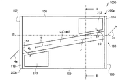
図1は、本発明を適用した実施形態に係る発光装置1000を模式的に示す平面図である。図2は、発光装置1000を模式的に示す断面図であり、図1のII−II線断面図である。
Figure 1 is a plan view schematically showing the engagement Ru emitting
本実施形態に係る発光装置1000は、図1および図2に示すように、同一基板10上に設けられた発光部100と受光部200a,200bとを含む。基板10は、例えば、第1導電型(例えばn型)のGaAs基板などを用いることができる。
Ru engaged in this embodiment
以下、発光部100および受光部200a,200bの構成、並びに発光装置1000の動作について説明する。
Hereinafter, the
(1)発光部の構成
発光部100は、図2に示すように、第1クラッド層104および第2クラッド層108に挟まれた活性層106と、第1電極120と、第2電極122と、を有する。発光部100は、さらに、第1コンタクト層109を有することができる。
(1) Configuration of Light Emitting Unit As illustrated in FIG. 2, the
第1クラッド層104は、基板10上に形成されている。第1クラッド層104は、例えば、第1導電型の半導体からなる。第1クラッド層104としては、例えばn型AlGaAs層などを用いることができる。なお、図示はしないが、基板10と第1クラッド層104との間に、バッファー層が形成されていてもよい。バッファー層としては、例えば基板10よりも結晶性の良好な(例えば欠陥密度の低い)第1導電型(n型)のGaAs層などを用いることができる。
The
活性層106は、第1クラッド層104上に形成されている。活性層106は、例えば、GaAsウェル層とAlGaAsバリア層とから構成される量子井戸構造を3つ重ねた多重量子井戸(MQW)構造を有する。
The
活性層106の一部は、利得領域を構成している。活性層106の形状は、例えば直方体(立方体である場合を含む)などであることができる。活性層106は、図1に示すように、第1側面105と、第1側面105に平行な第2側面107とを有する。利得領域140は、第1側面105に設けられた第1端面151と、第2側面107に設けられた第2端面152と、を有する。第1端面151および第2端面152には、例えば、反射防止膜110が設けられていることにより、低い反射率を得ることができる。反射防止膜110は、第1側面105および第2側面107の全面に設けられることができる。反射防止膜110としては、例えばAl2O3単層、または、SiO2層、SiN層、Ta2O5層や、これらの多層膜などを用いることができる。反射防止膜110は、膜厚および層数等を調整することにより、第1端面151および第2端面152の反射率を制御することができる。利得領域140の平面形状は、例えば図1に示すような平行四辺形などである。利得領域140は、図1に示すように平面的に見て、第1側面105から第2側面107まで、直線状に第1側面105の垂線Pに対して傾いた方向に向かって設けられている。これにより、利得領域140に生じる光のレーザー発振を抑制または防止することができる。
A part of the
図3は、活性層106を第1側面105側から平面的に見た図である。利得領域140では、図3に示すように第1側面105側から平面的に見て、第1端面151と第2端面152とが重なっていない。これにより、利得領域140に生じる光を、第1端面151と第2端面152との間で直接的に多重反射させないことができる。その結果、直接的な共振器を構成させないことができるため、利得領域140に生じる光のレーザー発振をより確実に抑制または防止することができる。したがって、発光装置1000は、レーザー光ではない光を発することができる。なお、この場合には、図3に示すように、例えば利得領域140において、第1端面151と第2端面152とのずれ幅xは、正の値であればよい。
FIG. 3 is a plan view of the
第2クラッド層108は、活性層106上に形成されている。第2クラッド層108は、例えば第2導電型(例えばp型)の半導体からなる。第2クラッド層108としては、例えばp型AlGaAs層などを用いることができる。
The
例えば、p型の第2クラッド層108、不純物がドーピングされていない活性層106、およびn型の第1クラッド層104により、pinダイオードが構成される。第1クラッド層104および第2クラッド層108の各々は、活性層106よりも禁制帯幅が大きく、屈折率が小さい層である。活性層106は、光を増幅する機能を有する。第1クラッド層104および第2クラッド層108は、活性層106を挟んで、注入キャリア(電子および正孔)並びに光を閉じ込める機能を有する。
For example, the p-type
第1コンタクト層109は、第2クラッド層108上に形成されている。第1コンタクト層109としては、第2電極122とオーミックコンタクトする層を用いることができる。第1コンタクト層109は、例えば第2導電型の半導体からなる。第1コンタクト層109としては、例えばp型GaAs層などを用いることができる。
The
第1電極120は、基板10の下に形成されていることができる。図2の例では、第1電極120は、基板10の下の全面に形成されている。第1電極120は、該第1電極120とオーミックコンタクトする層(図示の例では基板10)と接していることができる。第1電極120は、基板10を介して、第1クラッド層104と電気的に接続されている。第1電極120は、発光装置1000を駆動するための一方の電極である。第1電極120としては、例えば、基板10側からCr層、AuGe層、Ni層、Au層の順番で積層したものなどを用いることができる。第1電極120は、第3電極210と共通の電極であることができる。
The first electrode 120 may be formed under the
第2電極122は、第1コンタクト層109上に形成されている。第2電極122は、第1コンタクト層109を介して、第2クラッド層108と電気的に接続されている。第2電極122は、発光装置1000を駆動するための他方の電極である。第2電極122としては、例えば、第1コンタクト層109側からCr層、AuZn層、Au層の順番で積層したものなどを用いることができる。第2電極122の下面は、図1に示すように、利得領域140と同様の平面形状を有している。言い換えるならば、図示の例では、第2電極122の下面の平面形状によって、電極120、122間の電流経路が決定され、その結果、活性層106の利得領域140の平面形状が決定されるのである。あるいは、第1コンタクト層109上に絶縁層(図示せず)を形成した後に、利得領域140と同様の平面形状となるように該絶縁層を除去して第1コンタクト層109を露出させ、第2電極122を少なくとも露出した第1コンタクト層109と接触している形状となるように形成されていてもよい。
The
(2)受光部の構成
受光部200a,200bは、図1および図2に示すように、光吸収層206を含む。受光部200a,200bは、さらに、例えば、第3クラッド層204と、第4クラッド層208と、第2コンタクト層209と、第3電極210と、第4電極212と、を有することができる。
(2) Configuration of Light Receiving Part The
受光部200a,200bは、図1に示すように、活性層106の第1側面105側の第1受光部200aと、活性層106の第2側面107側の第2受光部200bとを有することができる。なお、受光部200a,200bは、活性層106のいずれか一方の側面側にのみ設けられていてもよい。第1受光部200aは、利得領域140の第1端面151で反射された第1反射光2bの光路上に配置されている。第2受光部200bは、利得領域140の第2端面152で反射された第2反射光4bの光路上に配置されている。第1受光部200aは、第1端面151の近傍に設けられることが望ましい。第2受光部200bについても同様に、第2端面152の近傍に設けられることが望ましい。これにより、反射光2b、4bが、受光部200a,200b以外の領域で吸収されることを抑制することができる。
As shown in FIG. 1, the
第3クラッド層204は、基板10上に形成されている。第3クラッド層204は、例えば、第1導電型の半導体からなる。第3クラッド層204としては、例えばn型AlGaAs層などを用いることができる。第3クラッド層204と第1クラッド層104とは、連続する一つの層からなることができる。
The
光吸収層206は、第3クラッド層204上に形成されている。光吸収層206としては、例えば、不純物がドーピングされていないGaAs層などを用いることができる。光吸収層206は、後述するように、利得領域140に生じる光の一部を、吸収することができる。光吸収層206と活性層106とは、連続する一つの層からなることができる。
The
第4クラッド層208は、光吸収層206上に形成されている。第4クラッド層208は、例えば第2導電型(例えばp型)の半導体からなる。第4クラッド層208としては、例えばp型AlGaAs層などを用いることができる。第4クラッド層208と第2クラッド層108とは、連続する一つの層からなることができる。
The
p型の第4クラッド層208、不純物がドーピングされていない光吸収層206、およびn型の第3クラッド層204により、pinダイオードが構成されることができる。第3クラッド層204および第4クラッド層208の各々は、光吸収層206よりも禁制帯幅が大きく、屈折率が小さい層である。光吸収層206は、光を吸収する機能を有する。第3クラッド層204および第4クラッド層208は、光吸収層206を挟んで、光を閉じ込める機能を有する。
The p-type
第2コンタクト層209は、第4クラッド層208上に形成されている。第2コンタクト層209としては、第2電極122とオーミックコンタクトする層を用いることができる。第2コンタクト層209は、例えば第2導電型の半導体からなる。第2コンタクト層209としては、例えばp型GaAs層などを用いることができる。第2コンタクト層209と、第1コンタクト層109とは、連続する一つの層からなることができる。
The
図2に示すように、受光部200a,200bの第3電極210から第4電極212までの層構造は、発光部100の第1電極120から第2電極122までの層構造と同じであることができる。
As shown in FIG. 2, the layer structure from the third electrode 210 to the
第3電極210は、基板10の下に形成されている。第3電極210は、図示の例では、第1電極120と共通の電極である。第3電極210は、受光部を駆動するための一方の電極である。第3電極210は、基板10を介して、第3クラッド層204と電気的に接続されている。第3電極210としては、第1電極120と同様の材料を用いることができる。
The third electrode 210 is formed under the
第4電極212は、第2コンタクト層209上に形成されている。第4電極212は、受光部を駆動するための他方の電極である。第4電極212は、第2コンタクト層209を介して、第4クラッド層208と電気的に接続されている。第4電極212としては、第2電極122と同様の材料を用いることができる。
The
(3)発光装置の動作
発光装置1000の発光部100では、第1電極120と第2電極122との間に、pinダイオードの順バイアス電圧を印加すると、活性層106の利得領域140において電子と正孔との再結合が起こる。この再結合により発光が生じる。この生じた光を起点として、連鎖的に誘導放出が起こり、利得領域140内で光の強度が増幅される。例えば、図1に示すように、利得領域140に生じる光のうち、第1端面151に向かう光2は、利得領域140内で増幅された後、第1端面151から第1出射光2aとして出射される。同様に、利得領域140に生じる光のうち、第2端面152に向かう光4は、利得領域140内で増幅された後、第2端面152から第2出射光4aとして出射される。ここで、第1端面151に向かう光2および第2端面152に向かう光4の一部は、第1端面151および第2端面152で反射され、第1反射光2bおよび第2反射光4bとして発光装置1000内を進行するものもある。すなわち、利得領域140に生じる光のうち、第1端面151に向かう光2は、第1端面151において、第1出射光2aと、第1反射光2bとに分けられる。第2端面152に向かう光4についても同様に、第2端面152において、第2出射光4aと、第2反射光4bとに分けられる。第1反射光2bは、発光装置1000内を進行して第1受光部200aに至る。第2反射光4bも同様に、発光装置1000内を進行して第2受光部200bに至る。なお、図1の例では、第1端面151および第2端面152の両方から光が出射される場合について説明したが、いずれか一方の端面から光が出射されてもよい。
(3) Operation of the light - emitting device
In the light-emitting
発光装置1000の受光部200a,200bでは、第3電極210と第4電極212との間に、pinダイオードの逆バイアス電圧を印加すると、反射光2b,4bによって光吸収層206に生成された電子−正孔対が加速され電流として取り出すことができる。これにより、受光部200a,200bは、発光部100に生じた光の光出力をモニターすることができる。さらに、第3クラッド層204および第4クラッド層208によって、光吸収層206から光が漏れることを抑制または防止することができる。
The
本実施形態に係る発光装置1000の一例として、GaAs系の場合について説明したが、発光装置1000は、発光利得領域が形成可能なあらゆる材料系を用いることができる。半導体材料であれば、例えば、InGaAlP系、AlGaN系、InGaN系、InGaAs系、GaInNAs系、ZnCdSe系などの半導体材料を用いることができる。
As an example of the engagement Ru emitting
本実施形態に係る発光装置1000は、例えば、プロジェクター、ディスプレイ、照明装置、計測装置などの光源に適用されることができる。
Engaging Ru emitting
発光装置1000は、例えば、以下の特徴を有する。
Light - emitting
本実施形態に係る発光装置1000では、発光部100と受光部200a,200bを同一基板10上に形成することができる。これにより、後述するように発光装置のアレイ化を、容易に行うことができる。また、例えば、別途、受光素子を設置する場合と比較して、部品点数の削減および製造コストの削減が可能となる。
In engaging Ru emitting
本実施形態に係る発光装置1000では、発光部100に生じた光の光出力を、受光部200a,200bにおいてモニターすることができる。したがって、モニターされた光出力に基づいて、発光部100に印加する電圧値を調整することができる。これにより、輝度むらを低減し、また、明るさを自動調整することができる発光装置を提供することができる。発光部100に生じた光の光出力を、発光部100に印加する電圧値にフィードバックする制御は、例えば、外部電子回路(図示しない)を用いて行うことができる。
In engaging Ru emitting
発光装置1000では、利得領域140の端面151,152で反射された反射光2b,4bを受光部200a,200bで受光することができる。したがって、発光部100から出射された光を直接モニターする場合と比較して、受光部200a,200bに至る光の光量が少ないため、発光部100の光出力を大きくすることができる。また、反射防止膜110によって、利得領域140の端面151,152の反射率を制御することができるため、受光部200a,200bに至る反射光2b、4bの光量を制御することができる。
In light - emitting
発光装置1000では、利得領域140は、第1側面105の垂線Pに対して傾いた方向に向かって設けられていることができる。さらに、利得領域140では、第1側面105側から平面的にみて、第1端面151と第2端面152とは、重なっていないことができる。これにより、上述したとおり、利得領域140に生じる光のレーザー発振を抑制または防止することができる。したがって、スペックルノイズを低減させることができる。さらに、発光装置1000では、利得領域140に生じる光は、利得領域140内において利得を受けながら進行して、外部に出射されることができる。したがって、従来の一般的なLED(Light Emitting Diode)よりも高い出力を得ることができる。以上のように、発光装置1000では、スペックルノイズを低減でき、かつ高出力化を図ることができる。
In light - emitting
2.発光装置の製造方法
次に、発光装置1000の製造方法の一例について、図面を参照しながら説明する。
2 . Method of manufacturing a light emission device Next, an example of a method for manufacturing a
図4は、発光装置1000の製造工程を模式的に示す断面図であり、図2に示す断面図に対応している。
Figure 4 is a cross-sectional view schematically showing a manufacturing process of the
図4に示すように、例えば、基板10上に、第1クラッド層104および第3クラッド層204を構成する層、活性層106および光吸収層206を構成する層、第2クラッド層108および第4クラッド層208を構成する層、および第1コンタクト層109および第2コンタクト層209を構成する層を、この順でエピタキシャル成長させる。エピタキシャル成長させる方法としては、例えば、MOCVD(Metal-Organic Chemical Vapor Deposition)法、MBE(Molecular Beam Epitaxy)法などを用いることができる。
As shown in FIG. 4, for example, on the
図2に示すように、例えば、第1コンタクト層109上に第2電極122および第4電極212を形成する。第2電極122および第4電極212は、例えば、真空蒸着法により全面に導電層を形成した後、該導電層をフォトリソグラフィ技術およびエッチング技術を用いてパターニングすることにより形成される。また、第2電極122および第4電極212は、例えば、真空蒸着法およびリフトオフ法の組み合わせなどにより、所望の形状に形成されることもできる。
As shown in FIG. 2, for example, the
次に、基板10の下面下に第1電極120および第3電極210を形成する。第1電極120および第3電極210は、例えば、上述した第2電極122の製法と同じ製法で形成される。
Next, the first electrode 120 and the third electrode 210 are formed under the lower surface of the
以上の工程により、発光装置1000が得られる。
Through the above process,
発光装置1000の製造方法によれば、発光部100を構成する層と受光部200a,200bを構成する層を同一工程で成膜することができる。したがって、発光部100を構成する層と受光部200a,200bを構成する層を別々に成膜する場合と比較して、製造工程を簡略化することができる。
According to the manufacturing method of the
発光装置1000の製造方法によれば、発光部および受光部を同一基板10上に集積することができる発光装置1000を形成することができる。
According to the manufacturing method of the
3.変形例
次に本実施形態に係る発光装置の変形例について説明する。なお、上述した図1〜図2に示す発光装置1000の例と異なる点について説明し、同様の点については同一の符号を付し説明を省略する。
3. Modification Next, a modification of the engagement Ru emitting light device according to the present embodiment will be described. Incidentally, omitted and description, the same points are denoted by the same reference numerals described example differs from the FIGS. 1-2 to indicate to light - emitting
(1)第1の変形例
まず、第1の変形例について説明する。
(1) First Modification First, a first modification will be described.
図5は、本変形例に係る発光装置2000を模式的に示す平面図である。図6は、図5のVI−VI線断面図であり、図2に対応している。
Figure 5 is a plan view of a engagement Ru - emitting
本変形例に係る発光装置2000では、発光部100と受光部200a,200bとを電気的に分離する分離溝220を有する。
In engaging Ru emitting
分離溝220は、図5に示すように、平面的に見て、第1受光部200aおよび第2受光部200bの各々の周囲を囲むように設けられている。図示はしないが、例えば、分離溝220は、平面的に見て、活性層106の第1側面105側から第2側面107側まで、発光部100と第1受光部200aとの間および発光部100と第2受光部200bとの間に直線状に設けられていてもよい。図6に示すように、分離溝220の底面の位置は、活性層106および光吸収層206の底面の位置より下であることができる。分離溝220の内部は、空隙(空気)であることができる。
As shown in FIG. 5, the
本変形例に係る発光装置2000では、発光部100と受光部200a,200bとを電気的に分離する分離溝220を有することができる。これにより、発光部100と受光部200a,200bとの間で電流拡散が起こりにくくなるため、発光部100と受光部200a,200bとの間の干渉を抑制することができる。また、分離溝220で発光部100と受光部200a,200bを電気的に分離できるため、図示はしないが、例えば、基板10として半絶縁性のGaAs基板等を用いた場合、発光部100と受光部200a,200bを独立駆動させることができる4端子構造を得ることができる。
In engaging Ru emitting
(2)第2の変形例
次に、第2の変形例について説明する。
(2) Second Modification Next, a second modification will be described.
図7は、本変形例に係る発光装置3000を模式的に示す断面図であり、図2に対応している。
7, the engaging Ru emitting
発光装置1000の例では、発光部100と受光部200a,200bとが、同じ層構造を有している場合について説明した。これに対し、本変形例では、発光部100と受光部200a,200bとが異なる層構造を有していることができる。
In the example of
図7に示すように、活性層106の膜厚は、例えば、光吸収層206の膜厚よりも薄い。より具体的には、活性層106の下面の位置は、光吸収層206の下面の位置より上方であり、活性層106の上面の位置は、光吸収層206の上面の位置より下方であることができる。これにより、本変形例に係る発光装置3000では、受光部200a,200bの光検出効率を向上させることができる。光吸収層206の膜厚は、例えば、活性層106の膜厚の2倍以上であることが望ましい。なお、受光部200a,200bの層構造は、特に限定されない。
As shown in FIG. 7, the film thickness of the
発光装置3000の製造方法は、まず、基板10上の全面に、第1クラッド層104、活性層106、第2クラッド層108、および第1コンタクト層109層を、この順でエピタキシャル成長させる。次に、基板10上の各層104,106,108,109をパターニングして、受光部200a,200bを設けられる領域の基板10を露出させる。その後、露出された基板10上および第2コンタクト層209上に、第3クラッド層204、光吸収層206、第4クラッド層208、および第2コンタクト層209層を、この順で成膜する。第1コンタクト層109上の各層は、エッチバックする。以後の工程は、発光装置1000の例と同様のため省略する。以上の工程により、発光装置3000が得られる。
Method of manufacturing a
(3)第3の変形例
次に、第3の変形例について説明する。
(3) Third Modification Next, a third modification will be described.
図8は、本変形例に係る発光装置4000を模式的に示す断面図であり、図2に対応している。 8, the engaging Ru emitting light device 4000 in this modification is a cross-sectional view schematically showing, and corresponds to FIG.
発光装置1000の例では、利得領域がそのまま導波領域となる利得導波型について説明した。それに対して、本変形例では、屈折率差を設けて光を閉じ込める屈折率導波型を用いることができる。
In the example of
第1コンタクト層109と、第2クラッド層108の一部とは、図8に示すように、柱状部160を構成することができる。柱状部160の平面形状は、例えば利得領域140と同じである。すなわち、例えば、柱状部160の平面形状によって、電極120,122間の電流経路が決定され、その結果、利得領域140の平面形状が決定される。なお、図示はしないが、柱状部160は、例えば、第1コンタクト層109、第2クラッド層108、および活性層106から構成されていてもよいし、さらに、第1クラッド層104をも含んで構成されていてもよい。また、柱状部160の側面を傾斜させることもできる。
The
絶縁部162は、図8に示すように、第2クラッド層108上であって、柱状部160の側方に形成されている。絶縁部162は、柱状部160の側面に接していることができる。絶縁部162の上面は、例えば、第1コンタクト層109の上面と連続している。絶縁部162としては、例えば、SiN層、SiO2層、ポリイミド層などを用いることができる。絶縁部162としてこれらの材料を用いた場合、電極120,122間の電流は、絶縁部162を避けて、該絶縁部162に挟まれた柱状部160を流れることができる。絶縁部162は、活性層106の屈折率よりも小さい屈折率を有することができる。この場合、絶縁部162を形成した部分の垂直断面の有効屈折率は、絶縁部162を形成しない部分、すなわち、柱状部160が形成された部分の垂直断面の有効屈折率よりも小さくなる。これにより、平面方向において、利得領域140内に効率良く光を閉じ込めることができる。なお、図示はしないが、絶縁部162を設けず、絶縁部162が空気であると解釈してもよい。
As shown in FIG. 8, the insulating part 162 is formed on the
第2電極122は、第1コンタクト層109(柱状部160)上および絶縁部162上に形成されている。第2電極122と第1コンタクト層109との接触面は、利得領域140と同じの平面形状を有している。図示はしないが、第2電極122は、第1コンタクト層109上にのみ形成されていてもよい。
The
本変形例によれば、上述した発光装置1000の例と同様に、発光部100と受光部200a,200bを同一基板上に形成した発光装置を得ることができる。
According to this modification, it is possible as in the example of
(4)第4の変形例
次に、第4の変形例について説明する。
(4) Fourth Modified Example Next, a fourth modified example will be described.
図9は、本変形例に係る発光装置5000を模式的に示す平面図である。
Figure 9 is a plan view schematically showing the engagement Ru emitting
発光装置5000では、図9に示すように、複数の利得領域140が配列されている。複数の利得領域140の各々に対応して、受光部200a,200bが設けられている。図示はしないが、発光装置5000は、複数の利得領域140の各々を電気的に分離する分離溝を有していてもよい。
In
発光装置5000によれば、発光装置1000の場合と比較して、発光の高出力化を図ることができる。
According to the
また、発光装置5000では、複数の利得領域140の各々に対応して、受光部200a,200bが設けられていることができる。したがって、複数の利得領域140の各々の光出力をモニターすることができる。すなわち、複数の利得領域140の各々に対して、個別に光量検出を行うことができる。
Further, the
なお、上述した変形例は一例であって、これらに限定されるわけではない。例えば、各実施形態および各変形例を適宜組み合わせることも可能である。 Note that the above-described modifications are merely examples, and the present invention is not limited to these. For example, it is possible to appropriately combine each embodiment and each modification.
上記のように、本発明の実施形態について詳細に説明したが、本発明の新規事項および効果から実体的に逸脱しない多くの変形が可能であることは当業者には容易に理解できよう。従って、このような変形例はすべて本発明の範囲に含まれるものとする。 Although the embodiments of the present invention have been described in detail as described above, those skilled in the art will readily understand that many modifications are possible without substantially departing from the novel matters and effects of the present invention. Accordingly, all such modifications are intended to be included in the scope of the present invention.
10 基板、100 発光部、104 第1クラッド層、105 第1側面、106 活性層、107 第2側面、108 第2クラッド層、109 第1コンタクト層、110 反射防止膜、120 第1電極、122 第2電極、140 利得領域、151 第1端面、152 第2端面、160 柱状部、162 絶縁部、200a,200b 受光部、204 第3クラッド層、206 光吸収層、208 第4クラッド層、209 第2コンタクト層、210 第3電極、212 第4電極、220 分離溝、1000,2000,3000,4000,5000 発光装置
DESCRIPTION OF
Claims (6)
前記発光部は、
第1クラッド層および第2クラッド層に挟まれた活性層と、
前記第1クラッド層に電気的に接続された第1電極と、
前記第2クラッド層に電気的に接続された第2電極と、
を有し、
前記受光部は、光吸収層を有し、
前記活性層の少なくとも一部は、前記第1電極と前記第2電極の間の電流経路に利得領域を構成し、
前記利得領域は、平面的に見て、前記活性層の第1側面から前記第1側面と平行な第2側面まで、前記第1側面の垂線に対して傾いた方向に延在し、
前記利得領域に生じる光は、前記利得領域の前記第1側面側の端面および前記第2側面側の端面の少なくとも一方において、外部に出射される光と、反射される光と、に分けられ、
前記反射される光は、前記受光部において受光され、
前記第1クラッド層、前記第2クラッド層および前記活性層を含む積層構造体が、平面的に見て、前記受光部の周囲を囲んで設けられ、
前記受光部と前記積層構造体とを電気的に分離する分離溝が、平面的に見て、前記受光部と前記積層構造体との間に、前記受光部の周囲を囲んで設けられる、発光装置。 Including a light emitting portion and a light receiving portion provided on the same substrate,
The light emitting unit
An active layer sandwiched between a first cladding layer and a second cladding layer;
A first electrode electrically connected to the first cladding layer;
A second electrode electrically connected to the second cladding layer;
Have
The light receiving unit has a light absorption layer,
At least a part of the active layer constitutes a gain region in a current path between the first electrode and the second electrode;
The gain region extends in a direction inclined with respect to a normal to the first side surface from a first side surface of the active layer to a second side surface parallel to the first side surface in plan view,
The light generated in the gain region is divided into light emitted to the outside and reflected light on at least one of the end surface on the first side surface side and the end surface on the second side surface side of the gain region,
The reflected light is received by the light receiving unit ,
A laminated structure including the first cladding layer, the second cladding layer, and the active layer is provided so as to surround the light receiving portion in a plan view.
A separation groove that electrically separates the light receiving unit and the stacked structure is provided between the light receiving unit and the stacked structure so as to surround the light receiving unit in plan view. apparatus.
前記受光部は、前記第1側面側と前記第2側面側とに設けられている、発光装置。 In claim 1,
The light receiving unit is a light emitting device provided on the first side surface side and the second side surface side.
前記活性層と前記光吸収層は、連続した1つの層である、発光装置。 In claim 1 or 2 ,
The light emitting device, wherein the active layer and the light absorption layer are one continuous layer.
前記活性層の下面の位置は、前記光吸収層の下面の位置より上方であり、
前記活性層の上面の位置は、前記光吸収層の上面の位置より下方である、発光装置。 In any one of Claims 1 thru | or 3 ,
The position of the lower surface of the active layer is above the position of the lower surface of the light absorption layer,
The position of the upper surface of the said active layer is a light-emitting device below the position of the upper surface of the said light absorption layer.
前記利得領域では、前記第1側面側から平面的に見て、前記第1側面側の端面と、前記第2側面側の端面とは、重なっていない、発光装置。 In any one of Claims 1 thru | or 4 ,
In the gain region, when viewed in plan from the first side surface side, the end surface on the first side surface side and the end surface on the second side surface side do not overlap.
前記利得領域は、複数配列され、
複数の前記利得領域の各々に対応して、前記受光部が設けられている、発光装置。 In any one of Claims 1 thru | or 5 ,
A plurality of the gain regions are arranged,
A light emitting device, wherein the light receiving unit is provided corresponding to each of the plurality of gain regions.
Priority Applications (3)
| Application Number | Priority Date | Filing Date | Title |
|---|---|---|---|
| JP2009113492A JP5447794B2 (en) | 2009-05-08 | 2009-05-08 | Light emitting device |
| US12/767,103 US8344393B2 (en) | 2009-05-08 | 2010-04-26 | Light receiving and emitting device |
| US13/693,624 US8629461B2 (en) | 2009-05-08 | 2012-12-04 | Light receiving and emitting device |
Applications Claiming Priority (1)
| Application Number | Priority Date | Filing Date | Title |
|---|---|---|---|
| JP2009113492A JP5447794B2 (en) | 2009-05-08 | 2009-05-08 | Light emitting device |
Publications (3)
| Publication Number | Publication Date |
|---|---|
| JP2010263109A JP2010263109A (en) | 2010-11-18 |
| JP2010263109A5 JP2010263109A5 (en) | 2012-06-21 |
| JP5447794B2 true JP5447794B2 (en) | 2014-03-19 |
Family
ID=43061841
Family Applications (1)
| Application Number | Title | Priority Date | Filing Date |
|---|---|---|---|
| JP2009113492A Expired - Fee Related JP5447794B2 (en) | 2009-05-08 | 2009-05-08 | Light emitting device |
Country Status (2)
| Country | Link |
|---|---|
| US (2) | US8344393B2 (en) |
| JP (1) | JP5447794B2 (en) |
Families Citing this family (8)
| Publication number | Priority date | Publication date | Assignee | Title |
|---|---|---|---|---|
| ES2363276T3 (en) | 2008-12-12 | 2011-07-28 | Amrona Ag | INERTIZATION OR EXTINGUISHING METHOD TO PREVENT AND / OR EXTINGUISH FIRE AND INERTIZATION SYSTEM TO IMPLEMENT THE METHOD. |
| JP5447794B2 (en) * | 2009-05-08 | 2014-03-19 | セイコーエプソン株式会社 | Light emitting device |
| JP5447799B2 (en) * | 2009-06-18 | 2014-03-19 | セイコーエプソン株式会社 | Light emitting device, driving method thereof, and projector |
| ITMI20111447A1 (en) | 2011-07-29 | 2013-01-30 | E T C Srl | ELECTROLUMINESCENT ORGANIC TRANSISTOR |
| ITMI20111446A1 (en) * | 2011-07-29 | 2013-01-30 | E T C Srl | ELECTROLUMINESCENT ORGANIC TRANSISTOR |
| US20140184062A1 (en) * | 2012-12-27 | 2014-07-03 | GE Lighting Solutions, LLC | Systems and methods for a light emitting diode chip |
| WO2016029104A1 (en) | 2014-08-22 | 2016-02-25 | Nse Products, Inc. | Selectively actuated fluid dispenser |
| US10840406B2 (en) * | 2017-04-17 | 2020-11-17 | Hamamatsu Photonics K.K. | Optical semiconductor element and method of driving optical semiconductor element |
Family Cites Families (13)
| Publication number | Priority date | Publication date | Assignee | Title |
|---|---|---|---|---|
| JPH0426159A (en) * | 1990-05-22 | 1992-01-29 | Ricoh Co Ltd | Semiconductor light-integration device |
| JPH0433386A (en) | 1990-05-30 | 1992-02-04 | Omron Corp | End surface emitting type semiconductor light emitting element and driving method therefor |
| JPH08162669A (en) | 1994-12-06 | 1996-06-21 | Nippondenso Co Ltd | Superluminescent diode |
| JPH103691A (en) | 1996-04-18 | 1998-01-06 | Matsushita Electric Ind Co Ltd | Optical pickup device |
| US6459716B1 (en) * | 2001-02-01 | 2002-10-01 | Nova Crystals, Inc. | Integrated surface-emitting laser and modulator device |
| KR100575964B1 (en) | 2003-12-16 | 2006-05-02 | 삼성전자주식회사 | Electro-absorptive optical modulator module with monolithic integrated photo detector |
| JP2005216954A (en) | 2004-01-27 | 2005-08-11 | Sumitomo Electric Ind Ltd | Semiconductor light element |
| JP5382289B2 (en) | 2008-03-26 | 2014-01-08 | セイコーエプソン株式会社 | Light emitting device |
| JP5168476B2 (en) | 2008-03-26 | 2013-03-21 | セイコーエプソン株式会社 | Light emitting device |
| JP2009238846A (en) | 2008-03-26 | 2009-10-15 | Seiko Epson Corp | Light-emitting device |
| JP5411440B2 (en) | 2008-03-26 | 2014-02-12 | セイコーエプソン株式会社 | Light emitting device |
| JP2009238845A (en) | 2008-03-26 | 2009-10-15 | Seiko Epson Corp | Light-emitting module and method of manufacturing the same |
| JP5447794B2 (en) * | 2009-05-08 | 2014-03-19 | セイコーエプソン株式会社 | Light emitting device |
-
2009
- 2009-05-08 JP JP2009113492A patent/JP5447794B2/en not_active Expired - Fee Related
-
2010
- 2010-04-26 US US12/767,103 patent/US8344393B2/en not_active Expired - Fee Related
-
2012
- 2012-12-04 US US13/693,624 patent/US8629461B2/en not_active Expired - Fee Related
Also Published As
| Publication number | Publication date |
|---|---|
| JP2010263109A (en) | 2010-11-18 |
| US8344393B2 (en) | 2013-01-01 |
| US20100283063A1 (en) | 2010-11-11 |
| US8629461B2 (en) | 2014-01-14 |
| US20130092959A1 (en) | 2013-04-18 |
Similar Documents
| Publication | Publication Date | Title |
|---|---|---|
| JP5447794B2 (en) | Light emitting device | |
| JP5196179B2 (en) | Light emitting device | |
| JP2010263109A5 (en) | ||
| JP4962743B2 (en) | Light emitting device | |
| JP5257604B2 (en) | Light emitting device | |
| JP5088498B2 (en) | Light emitting device | |
| JP5187525B2 (en) | Light emitting device | |
| JP5088499B2 (en) | Light emitting device | |
| US8194714B2 (en) | Light emitting and receiving device | |
| JP2009238828A (en) | Light emitting device | |
| JP2011066138A (en) | Projector | |
| JP2010212347A (en) | Light receiving/emitting device | |
| US20100237358A1 (en) | Light-emitting device and light-emitting module | |
| JP2010161104A (en) | Light emitting device and layered light emitting device | |
| JP2009238845A (en) | Light-emitting module and method of manufacturing the same | |
| JP2009238846A (en) | Light-emitting device | |
| JP5168476B2 (en) | Light emitting device | |
| JP2010141241A (en) | Method for manufacturing light-emitting device and the light-emitting device | |
| JP5534259B2 (en) | Light emitting device | |
| JP5403305B2 (en) | Light emitting device | |
| JP2010219199A (en) | Light receiving/emitting device | |
| JP5445803B2 (en) | Light emitting device | |
| JP2010267642A (en) | Light emitting device | |
| JP2015087693A (en) | Light-emitting device and projector | |
| JP2013038446A (en) | Light-emitting device |
Legal Events
| Date | Code | Title | Description |
|---|---|---|---|
| A521 | Request for written amendment filed |
Free format text: JAPANESE INTERMEDIATE CODE: A523 Effective date: 20120502 |
|
| A621 | Written request for application examination |
Free format text: JAPANESE INTERMEDIATE CODE: A621 Effective date: 20120502 |
|
| A131 | Notification of reasons for refusal |
Free format text: JAPANESE INTERMEDIATE CODE: A131 Effective date: 20130724 |
|
| A977 | Report on retrieval |
Free format text: JAPANESE INTERMEDIATE CODE: A971007 Effective date: 20130724 |
|
| A521 | Request for written amendment filed |
Free format text: JAPANESE INTERMEDIATE CODE: A523 Effective date: 20130924 |
|
| TRDD | Decision of grant or rejection written | ||
| A01 | Written decision to grant a patent or to grant a registration (utility model) |
Free format text: JAPANESE INTERMEDIATE CODE: A01 Effective date: 20131204 |
|
| A61 | First payment of annual fees (during grant procedure) |
Free format text: JAPANESE INTERMEDIATE CODE: A61 Effective date: 20131217 |
|
| R150 | Certificate of patent or registration of utility model |
Free format text: JAPANESE INTERMEDIATE CODE: R150 |
|
| S531 | Written request for registration of change of domicile |
Free format text: JAPANESE INTERMEDIATE CODE: R313531 |
|
| R350 | Written notification of registration of transfer |
Free format text: JAPANESE INTERMEDIATE CODE: R350 |
|
| LAPS | Cancellation because of no payment of annual fees |