EP2573822A1 - Semiconductor device, and method for producing semiconductor device - Google Patents
Semiconductor device, and method for producing semiconductor device Download PDFInfo
- Publication number
- EP2573822A1 EP2573822A1 EP11783455A EP11783455A EP2573822A1 EP 2573822 A1 EP2573822 A1 EP 2573822A1 EP 11783455 A EP11783455 A EP 11783455A EP 11783455 A EP11783455 A EP 11783455A EP 2573822 A1 EP2573822 A1 EP 2573822A1
- Authority
- EP
- European Patent Office
- Prior art keywords
- semiconductor substrate
- diffusion region
- masking paste
- type
- dopant diffusion
- Prior art date
- Legal status (The legal status is an assumption and is not a legal conclusion. Google has not performed a legal analysis and makes no representation as to the accuracy of the status listed.)
- Granted
Links
Images






Classifications
-
- H—ELECTRICITY
- H10—SEMICONDUCTOR DEVICES; ELECTRIC SOLID-STATE DEVICES NOT OTHERWISE PROVIDED FOR
- H10F—INORGANIC SEMICONDUCTOR DEVICES SENSITIVE TO INFRARED RADIATION, LIGHT, ELECTROMAGNETIC RADIATION OF SHORTER WAVELENGTH OR CORPUSCULAR RADIATION
- H10F10/00—Individual photovoltaic cells, e.g. solar cells
- H10F10/10—Individual photovoltaic cells, e.g. solar cells having potential barriers
- H10F10/14—Photovoltaic cells having only PN homojunction potential barriers
- H10F10/146—Back-junction photovoltaic cells, e.g. having interdigitated base-emitter regions on the back side
-
- B—PERFORMING OPERATIONS; TRANSPORTING
- B24—GRINDING; POLISHING
- B24B—MACHINES, DEVICES, OR PROCESSES FOR GRINDING OR POLISHING; DRESSING OR CONDITIONING OF ABRADING SURFACES; FEEDING OF GRINDING, POLISHING, OR LAPPING AGENTS
- B24B27/00—Other grinding machines or devices
- B24B27/06—Grinders for cutting-off
- B24B27/0633—Grinders for cutting-off using a cutting wire
-
- H—ELECTRICITY
- H10—SEMICONDUCTOR DEVICES; ELECTRIC SOLID-STATE DEVICES NOT OTHERWISE PROVIDED FOR
- H10F—INORGANIC SEMICONDUCTOR DEVICES SENSITIVE TO INFRARED RADIATION, LIGHT, ELECTROMAGNETIC RADIATION OF SHORTER WAVELENGTH OR CORPUSCULAR RADIATION
- H10F71/00—Manufacture or treatment of devices covered by this subclass
- H10F71/121—The active layers comprising only Group IV materials
-
- H—ELECTRICITY
- H10—SEMICONDUCTOR DEVICES; ELECTRIC SOLID-STATE DEVICES NOT OTHERWISE PROVIDED FOR
- H10F—INORGANIC SEMICONDUCTOR DEVICES SENSITIVE TO INFRARED RADIATION, LIGHT, ELECTROMAGNETIC RADIATION OF SHORTER WAVELENGTH OR CORPUSCULAR RADIATION
- H10F77/00—Constructional details of devices covered by this subclass
- H10F77/20—Electrodes
- H10F77/206—Electrodes for devices having potential barriers
- H10F77/211—Electrodes for devices having potential barriers for photovoltaic cells
- H10F77/219—Arrangements for electrodes of back-contact photovoltaic cells
-
- Y—GENERAL TAGGING OF NEW TECHNOLOGICAL DEVELOPMENTS; GENERAL TAGGING OF CROSS-SECTIONAL TECHNOLOGIES SPANNING OVER SEVERAL SECTIONS OF THE IPC; TECHNICAL SUBJECTS COVERED BY FORMER USPC CROSS-REFERENCE ART COLLECTIONS [XRACs] AND DIGESTS
- Y02—TECHNOLOGIES OR APPLICATIONS FOR MITIGATION OR ADAPTATION AGAINST CLIMATE CHANGE
- Y02E—REDUCTION OF GREENHOUSE GAS [GHG] EMISSIONS, RELATED TO ENERGY GENERATION, TRANSMISSION OR DISTRIBUTION
- Y02E10/00—Energy generation through renewable energy sources
- Y02E10/50—Photovoltaic [PV] energy
- Y02E10/547—Monocrystalline silicon PV cells
-
- Y—GENERAL TAGGING OF NEW TECHNOLOGICAL DEVELOPMENTS; GENERAL TAGGING OF CROSS-SECTIONAL TECHNOLOGIES SPANNING OVER SEVERAL SECTIONS OF THE IPC; TECHNICAL SUBJECTS COVERED BY FORMER USPC CROSS-REFERENCE ART COLLECTIONS [XRACs] AND DIGESTS
- Y02—TECHNOLOGIES OR APPLICATIONS FOR MITIGATION OR ADAPTATION AGAINST CLIMATE CHANGE
- Y02P—CLIMATE CHANGE MITIGATION TECHNOLOGIES IN THE PRODUCTION OR PROCESSING OF GOODS
- Y02P70/00—Climate change mitigation technologies in the production process for final industrial or consumer products
- Y02P70/50—Manufacturing or production processes characterised by the final manufactured product
Definitions
- the present invention relates to a semiconductor device and a method for manufacturing the semiconductor device.
- a double-sided electrode type solar cell has been a conventional mainstream solar cell, which includes for example a monocrystalline or polycrystalline silicon substrate having a light receiving surface having an impurity of a conduction type opposite to that of the silicon substrate diffused therein to provide a pn junction, and electrodes provided at the light receiving surface of the silicon substrate and a surface opposite to the light receiving surface, respectively.
- the double-sided electrode type solar cell it is also generally done to diffuse an impurity of the same conduction type as the silicon substrate in the silicon substrate at the back surface at a high concentration to provide high output by a back surface field effect.
- Patent Literature 1 Japanese Patent Laying-Open No. 2007-049079
- masking paste 102 is screen-printed on the entire surface of an n-type or p-type conductive semiconductor substrate 101 on the light receiving surface side and then dried, masking paste 102 is screen-printed on the surface of semiconductor substrate 101 on the back surface side so as to have an opening 114 partially provided therein.
- an n-type dopant 104 is diffused through opening 114 in the back surface of semiconductor substrate 101, thereby forming an n-type dopant diffusion region 103.
- masking paste 102 of semiconductor substrate 101 on each of the light receiving surface side and the back surface side is entirely removed.
- masking paste 102 is again screen-printed on the entire surface of semiconductor substrate 101 on the light receiving surface side and then dried, masking paste 102 is screen-printed on the surface of semiconductor substrate 101 on the back surface side so as to have an opening 115 partially provided therein.
- a p-type dopant 106 is diffused through opening 115 in the back surface of semiconductor substrate 101, thereby forming a p-type dopant diffusion region 105.
- a textured structure 108 is formed by texture-etching of the surface of semiconductor substrate 101 on the light receiving surface side, an antireflection film 109 is formed on textured structure 108 while a passivation film 107 is formed on the back surface side of semiconductor substrate 101.
- the conventional back electrode type solar cell causes a problem that n-type dopant diffusion region 103 and p-type dopant diffusion region 105 cannot be formed in their respective prescribed regions, so that excellent characteristics cannot be achieved with stability.
- the above-described problem occurs not only in the back electrode type solar cell but also, as a whole, in the semiconductor device including a solar cell such as a double-sided electrode type solar cell.
- the present invention aims to provide a semiconductor device capable of achieving excellent characteristics with stability, and a method for manufacturing the semiconductor device.
- the present invention provides a semiconductor device including a semiconductor substrate; and a dopant diffusion region provided in one surface of the semiconductor substrate.
- the semiconductor substrate has an abrasion trace formed on the surface thereof.
- the dopant diffusion region has a portion extending in a direction at an angle within a range of -5° to +5° with respect to a direction in which the abrasion trace extends.
- the dopant diffusion region includes an n-type dopant diffusion region and a p-type dopant diffusion region
- the semiconductor device further includes an electrode for n type disposed on the n-type dopant diffusion region and an electrode for p type disposed on the p-type dopant diffusion region.
- the present invention provides a method for manufacturing a semiconductor device.
- the method includes the steps of: forming an abrasion trace extending in one direction on a surface of a semiconductor substrate; placing, on a part of the surface of the semiconductor substrate, masking paste having a portion extending in a direction at an angle within a range of -5° to +5° with respect to a direction in which the abrasion trace extends; and forming a dopant diffusion region in a surface of the semiconductor substrate exposed from the masking paste.
- the step of forming the abrasion trace includes the step of cutting a semiconductor crystal ingot by a wire saw.
- the method for manufacturing a semiconductor device of the present invention includes the step of etching the surface of the semiconductor substrate between the step of forming the abrasion trace and the step of placing the masking paste.
- the present invention can provide a semiconductor device capable of achieving excellent characteristics with stability, and a method for manufacturing the semiconductor device.
- Figs. 1 to 17 explained will be a method for manufacturing a back electrode type solar cell in an embodiment that is an example of the method for manufacturing a semiconductor device according to the present invention.
- the same or corresponding components are designated by the same reference characters.
- the step of cutting a semiconductor crystal ingot 50 by a wire saw 53 is performed.
- wire saw 53 is wound across between guide rollers 51 and 52 that are disposed at a prescribed distance from each other. This brings about the state where wire saw 53 is tensioned by guide rollers 51 and 52 at a plurality of positions that are at a prescribed distance from one another in the longitudinal direction of each of guide rollers 51 and 52. In this state, guide rollers 51 and 52 repeatedly rotate in the normal direction and in the reverse direction, so that wire saw 53 reciprocates in the direction shown by an arrow 55.
- Semiconductor crystal ingot 50 is moved in the direction shown by an arrow 54 while wire saw 53 is reciprocating in the direction shown by arrow 55. Then, semiconductor crystal ingot 50 is pressed against reciprocating wire saw 53, thereby cutting semiconductor crystal ingot 50 at a plurality of positions and into a plurality of pieces of semiconductor substrates 1, for example, as shown in the schematic perspective view in Fig. 2 .
- Fig. 3 shows a schematic cross-sectional view of an example of wire saw 53 shown in Fig. 1 .
- wire saw 53 includes a core wire 53a and an abrasive grain 53b bonded to the outer circumferential surface of core wire 53a with the bond material (not shown).
- Core wire 53a may be made, for example, of a piano wire and the like.
- Abrasive grain 53b may be made, for example, of a diamond abrasive grain and the like.
- the bond material may be made, for example, of nickel and the like that is plated on the outer surface of core wire 53a.
- Fig. 4 shows a schematic cross-sectional view of an example of a semiconductor substrate 1 obtained by cutting semiconductor crystal ingot 50 by wire saw 53.
- the surface of semiconductor substrate 1 undergoes slice damage 1 a that is caused by cutting semiconductor crystal ingot 50 using the above-described wire saw 53.
- Examples of semiconductor crystal ingot 50 may be a crystal silicon ingot such as a single crystal silicon ingot produced by the Czochralski method or a polycrystal silicon ingot produced by the casting method.
- a crystal silicon ingot is used as semiconductor crystal ingot 50, a silicon crystal substrate can be obtained as semiconductor substrate 1. It is to be noted that semiconductor crystal ingot 50 has an n-type conductivity by an n-type dopant doped therein.
- slice damage 1a on the surface of semiconductor substrate 1 shown in Fig. 4 is performed.
- slice damage 1a can be removed, for example, by etching with an alkaline aqueous solution such as a sodium hydroxide aqueous solution or a potassium hydroxide aqueous solution.
- semiconductor substrate 1 may have a quadrangular surface, for example, having a thickness of 100 ⁇ m or more and 300 ⁇ m or less and having a side of 100 mm or more and 200 mm or less in length.
- Fig. 6 shows a schematic enlarged cross-sectional view of an example of a part of the surface of semiconductor substrate 1 shown in Fig. 5 .
- Fig. 7 shows a schematic perspective view of an example of a part of the surface of semiconductor substrate 1 shown in Fig. 5 .
- a relatively large meandering line an imaginary dashed line in Fig. 6 ; which will be hereinafter referred to as a "saw mark" 61 is formed while a groove-shaped abrasion trace 62 is formed that is less in depth than saw mark 61.
- Saw mark 61 is formed due to cutting of semiconductor crystal ingot 50 using wire saw 53.
- semiconductor substrate 1 is obtained by pressing semiconductor crystal ingot 50 against reciprocating wire saw 53, in which case, however, wire saw 53 is temporarily stopped to cause reduction in linear velocity each time a moving direction 55 of wire saw 53 is changed.
- This causes a difference in the depth cut into semiconductor crystal ingot 50 by wire saw 53 along the direction in which semiconductor crystal ingot 50 is moved toward wire saw 53 (the direction shown by arrow 54), which leads to occurrence of saw mark 61 emerged as a relatively large meandering line on the surface of semiconductor substrate 1.
- abrasion trace 62 is a scratch formed by abrasive grain 53b on wire saw 53 during cutting of semiconductor crystal ingot 50 using wire saw 53, which is formed in a groove shape extending in moving direction 55 of wire saw 53.
- a crater-shaped recess may be provided in the surface of semiconductor substrate 1 by etching performed for removing the above-described slice damage 1a.
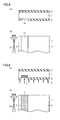
- masking paste 2 is placed on the entire surface (light receiving surface) of semiconductor substrate 1 on the light receiving surface side while masking paste 2 is placed on the surface (back surface) of semiconductor substrate 1 on the back surface side so as to have an opening 14 provided in masking paste 2.
- masking paste 2 is placed so as to have a portion extending in the direction at an angle within the range of -5 to +5° with respect to the direction in which the abrasion trace (not shown) extends (the direction shown by arrow 55). This is based on the inventors' finding obtained as a result of an earnest study, as follows.
- masking paste 2 in the case where masking paste 2 is placed so as to extend in the direction at an angle within the range of -5° to +5° with respect to the direction in which the abrasion trace extends, masking paste 2 can be suppressed from flowing out in the direction other than the extending direction of masking paste 2, as compared with the case where masking paste 2 is placed so as to extend in the direction at an angle beyond the above-described range. Accordingly, at least in the above-described portion of masking paste 2, opening 14 can be provided with stability in the direction at an angle within the range of -5° to + 5° with respect to the direction in which the abrasion trace extends (the direction shown by arrow 55). In the present embodiment, an explanation will be given with regard to the case where masking paste 2 is formed in a strip shape extending in the direction at an angle of 0° with respect to the direction in which the abrasion trace extends (the direction shown by arrow 55).
- Examples of the material for masking paste 2 may be a solvent, a thickening agent, and a silicon oxide precursor and/or a titanium oxide precursor, and furthermore, may be those not including a thickening agent.
- the solvent may be ethylene glycol, methyl cellosolve, methyl cellosolve acetate, ethyl cellosolve, diethyl cellosolve, cellosolve acetate, ethylene glycol mono-phenyl ether, methoxy ethanol, ethylene glycol monoacetate, ethylene glycol diacetate, diethylene glycol, diethylene glycol monomethyl ether, diethylene glycol monoethyl ether acetate, diethylene glycol monobutyl ether, diethylene glycol monobutyl ether acetate, diethylene glycol dimethyl ether, diethylene glycol methyl ethyl ether, diethylene glycol diethyl ether, diethylene glycol acetate, triethyl glycol, triethylene glycol monomethyl ether, triethylene glycol monoethyl ether, tetraethylene glycol, liquid polyethylene glycol, propylene glycol, propylene glycol monomethyl ether, propylene glycol monoethyl a
- the thickening agent may be bentonite with various qualities and characteristics, a rheology additive that is generally inorganic and used for various polar solvent mixtures, cellulose nitrate and other cellulose compounds, starch, gelatin, alginic acid, highly-dispersive amorphous silicic acid (Aerosil (registered trademark)), polyvinyl butyral (Mowital (registered trademark)), sodium carboxymethyl cellulose (vivistar), thermoplastic polyamide resin (Eurelon (registered trademark)), an organic castor oil dielectric (Thixin R (registered trademark)), diamide wax (Thixatrol plus (registered trademark)), swelling polyacrylate (Rheolate (registered trademark)), polyether urea-polyurethane, polyether polyol, and the like.
- a rheology additive that is generally inorganic and used for various polar solvent mixtures, cellulose nitrate and other cellulose compounds, starch, gelatin, algin
- Examples of the silicon oxide precursor may be substances like TEOS (tetraethyl orthosilicate) represented by a general formula R 1' n Si(OR 1 ) 4-n (wherein R 1' represents methyl, ethyl or phenyl; R 1 represents methyl, ethyl, n-propyl, or i-propyl; and n represents 0, 1 or 2).
- TEOS tetraethyl orthosilicate
- the titanium oxide precursor may be substances like TPT (tetraisopropoxy titanium) represented by R 2' n Ti(OR 2 ) 4-n (wherein R 2' represents methyl, ethyl or phenyl; R 2 represents methyl, ethyl, n-propyl, or i-propyl; and n represents 0, 1 or 2), and furthermore, may include TiCl 4 , TiF 4 , TiOSO 4 , and the like.
- TPT tilt titanium
- examples thereof may be castor oil, bentonite, cellulose nitrate, ethyl cellulose, polyvinyl pyrrolidone, starch, gelatin, alginic acid, amorphous silicic acid, polyvinyl butyral, sodium carboxymethyl cellulose, a polyamide resin, an organic castor oil dielectric, diamide wax, swelling polyacrylate, polyether urea-polyurethane, polyether polyol, and the like, which can be used alone or in combination with two or more of them.
- the method of placing masking paste 2 is not particularly limited, but, for example, a conventionally known coating method and the like can be used.
- Masking paste 2 placed on each of the light receiving surface and the back surface of semiconductor substrate 1 is dried.
- Masking paste 2 can be dried, for example, by placing semiconductor substrate 1 having masking paste 2 placed therein within an oven, and heating masking paste 2, for example, at a temperature of about 300 °C, for example, for several dozen minutes.
- masking paste 2 that has been dried as described above is fired, and thereby solidified.
- Masking paste 2 can be fired by heating masking paste 2, for example, at a temperature of 800 °C or higher and 1000 °C or lower, for example, for 10 minutes or more and 60 minutes or less.
- n-type dopant containing gas 4 is applied to cause the n-type dopant to be diffused in the back surface of semiconductor substrate 1 exposed through opening 14 on the back surface side of semiconductor substrate 1, thereby forming an n-type dopant diffusion region 3. Consequently, as shown in the schematic plan view in Fig. 9(b) , n-type dopant diffusion region 3 is formed in a strip shape extending in the direction at an angle within the range of -5° to +5° with respect to the direction in which the abrasion trace extends (the direction shown by arrow 55).
- n-type dopant containing gas 4 may be, for example, POCl 3 containing phosphorus that is an n-type dopant, and the like. Furthermore, n-type dopant diffusion region 3 is higher in n-type dopant concentration than semiconductor substrate 1.
- masking paste 2 on each of the light receiving surface and the back surface of semiconductor substrate 1 is entirely removed.
- Masking paste 2 can be removed, for example, by the process such as immersing semiconductor substrate 1 having masking paste 2 placed therein in a hydrofluoric acid aqueous solution.
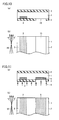
- masking paste 2 is placed on the entire surface (light receiving surface) of semiconductor substrate 1 on the light receiving surface side while masking paste 2 is also placed on the surface (back surface) of semiconductor substrate 1 on the back surface side so as to have an opening 15 provided in masking paste 2. Opening 15 is provided at a position different from that where opening 14 is provided.
- masking paste 2 is placed to have a portion extending in the direction at an angle within the range of -5° to +5° with respect to the direction in which the abrasion trace (not shown) extends (the direction shown by arrow 55). Consequently, at least in the above-described portion of masking paste 2, opening 15 can be provided with stability in the direction at an angle within the range of -5° to +5° with respect to the direction in which the abrasion trace extends (the direction shown by arrow 55).
- masking paste 2 is formed in a strip shape extending in the direction at an angle of 0° with respect to the direction in which the abrasion trace extends (the direction shown by arrow 55), which will be explained below.
- masking paste 2 After drying masking paste 2 applied onto each of the light receiving surface and the back surface of semiconductor substrate 1, masking paste 2 is fired and thereby solidified.
- p-type dopant containing gas 6 is applied to cause the p-type dopant to be diffused in the back surface of semiconductor substrate 1 exposed through opening 15 on the back surface side of semiconductor substrate 1, thereby forming a p-type dopant diffusion region 5. Consequently, as shown in the schematic plan view in Fig. 11(b) , p-type dopant diffusion region 5 is formed in a strip shape extending in the direction at an angle within the range of -5° to +5° with respect to the direction in which the abrasion trace extends (the direction shown by arrow 55). It is to be noted that examples of p-type dopant containing gas 6 may be BBr 3 containing boron that is a p-type dopant, for example.
- n-type dopant diffusion region 3 and p-type dopant diffusion region 5 each having a strip shape extending in the direction at an angle within the range of -5° to +5° with respect to the direction in which the abrasion trace extends (the direction shown by arrow 55).
- a passivation film 7 is formed on the back surface of semiconductor substrate 1.
- Examples of passivation film 7 may be a silicon oxide film, a silicon nitride film, or a silicon oxide film and a silicon nitride film stacked in layers, or the like.
- Passivation film 7 can be formed, for example, by the plasma CVD method or the like.
- a textured structure 8 is formed by texture etching of the light receiving surface of semiconductor substrate 1 on the side opposite to the side on which passivation film 7 is formed.
- Texture etching for forming textured structure 8 can be performed by using passivation film 7 as an etching mask that is formed on the surface of semiconductor substrate 1 on the other side.
- texture etching can be performed by etching the light receiving surface of semiconductor substrate 1 using the etching solution obtained by heating, for example to 70 °C or higher and 80 °C or lower, the solution obtained by adding isopropyl alcohol to an alkaline aqueous solution containing, for example, sodium hydroxide, potassium hydroxide or the like.
- an antireflection film 9 is formed on textured structure 8 of semiconductor substrate 1.
- antireflection film 9 may be a silicon oxide film, a silicon nitride film, or a silicon oxide film and a silicon nitride film stacked in layers, or the like.
- Antireflection film 9 can be formed, for example, by the plasma CVD method or the like.
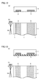
- a part of passivation film 7 is removed to form contact holes 10 and 11, thereby exposing a part of n-type dopant diffusion region 3 through contact hole 10 while exposing a part of p-type dopant diffusion region 5 through contact hole 11.
- Contact holes 10 and 11 can be formed, for example, by the method using the photolithography technique to form, on passivation film 7, a resist pattern having an opening in a portion corresponding to the portion where each of contact holes 10 and 11 is provided, and then, removing passivation film 7 from the opening of the resist pattern by means of etching.
- an electrode for n type 12 is formed that is electrically connected to n-type dopant diffusion region 3 via contact hole 10 while an electrode for p type 13 is formed that is electrically connected to p-type dopant diffusion region 5 via contact hole 11.
- electrode for n type 12 and electrode for p type 13 each can be an electrode, for example, made of metal such as silver. Consequently, the back electrode type solar cell in the present embodiment can be produced.
- masking paste 2 can be placed so as to have a portion extending in the direction at an angle within the range of -5° to +5° with respect to the direction in which the abrasion trace extends, as described above. Accordingly, at least in this portion of masking paste 2, openings 14 and 15 each can be provided in a stable shape extending in the direction at an angle within the range of -5° to +5° with respect to the direction in which the abrasion trace extends.
- n-type dopant diffusion region 3 and p-type dopant diffusion region 5 formed in openings 14 and 15, respectively, can also be formed in the desired shape with stability, so that the resultant back electrode type solar cell can achieve excellent characteristics with stability.
- the semiconductor crystal ingot having an n-type conductivity has been described in the above-described embodiment, the semiconductor crystal ingot may have a p-type conductivity.
- the present invention is not limited to the back electrode type solar cell, but can also be applied to a semiconductor device including a solar cell of any configuration such as a double-sided electrode type solar cell manufactured to include a semiconductor substrate having an electrode formed on each of its light receiving surface and its back surface.
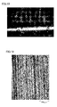
- an n-type polycrystal silicon ingot formed by the casting method was pressed against a reciprocating wire saw (having a shape shown in the enlarged photograph in Fig. 18 ), and then, the ingot was cut.
- This causes formation of a plurality of n-type polycrystalline silicon substrates each having a thickness of 200 ⁇ m, in which an abrasion trace was formed in the form of a groove extending in one direction on the light receiving surface and the back surface each having a quasi-square shape having each side of 126 mm in length.
- the wire saw used in this case shown in Fig. 18 was produced by bonding diamond abrasive grains each having a grain size of 30 ⁇ m or less onto the outer surface of the piano wire having a cross-sectional diameter of 120 ⁇ m with nickel plated on this outer surface.
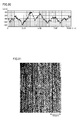
- Fig. 19 shows a microphotograph of an example of the surface of the n-type polycrystalline silicon substrate after being cut by the above-described wire saw.
- Fig. 20 shows the result of measuring concavities and convexities on the surface of the n-type polycrystalline silicon substrate shown in Fig. 19 by the laser microscope.
- the horizontal axis shows the width of the surface of the n-type polycrystalline silicon substrate (maximum width: 10 mm) while the vertical axis shows the thickness of the surface of the n-type polycrystalline silicon substrate (maximum thickness: 10 ⁇ m).
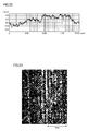
- Fig. 21 shows a microphotograph of another example of the surface of the n-type polycrystalline silicon substrate after being cut by the above-described wire saw.
- Fig. 22 shows the result of measuring concavities and convexities on the surface of the n-type polycrystalline silicon substrate shown in Fig. 21 by the laser microscope.
- the horizontal axis shows the width of the surface of the n-type polycrystalline silicon substrate (maximum width: 10 mm) while the vertical axis shows the thickness of the surface of the n-type polycrystalline silicon substrate (maximum thickness: 10 ⁇ m).
- Figs. 19 to 22 it was confirmed that saw marks and abrasion traces were formed on the surface of the n-type polycrystalline silicon substrate, in which case the saw marks each were a relatively large meandering line formed along the direction in which the n-type polycrystal silicon ingot was pressed against the wire saw while the abrasion traces (vertical lines in Figs. 19 and 21 ) each were in the shape of a groove formed in the saw mark along the direction in which the wire saw was moved.
- the surface of the n-type polycrystalline silicon substrate formed as described above was etched to a depth of 30 ⁇ m by the sodium hydroxide aqueous solution having a sodium hydroxide concentration of 48 percent by mass (a ratio of sodium hydroxide 48g to water 52g), thereby removing the slice damage on the surface of the n-type polycrystalline silicon substrate.
- Fig. 23 shows a microphotograph of an example of the etched surface of the n-type polycrystalline silicon substrate shown in Fig. 19 .
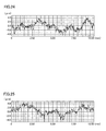
- Fig. 24 shows the result of measuring concavities and convexities on the surface of the n-type polycrystalline silicon substrate shown in Fig. 23 by the laser microscope.
- Fig. 25 shows the result of measuring concavities and convexities on the etched surface of the n-type polycrystalline silicon substrate shown in Fig. 21 by the laser microscope.
- circular recesses were formed on the surface of the n-type polycrystalline silicon substrate.
- abrasion traces did not disappear from the surface of the n-type polycrystalline silicon substrate.
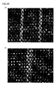
- a plurality of strip-shaped masking pastes (design width per masking paste: 1300 ⁇ m, viscosity: 13 Pa•S) were intermittently placed on the surface of the n-type polycrystalline silicon substrate that has been etched as described above, such that the masking pastes extended in the direction at an angle within the range of -5° to +5° with respect to the direction in which the abrasion trace extended.
- Fig. 26 (a) shows a microphotograph of the surface of the n-type polycrystalline silicon substrate in which masking paste is placed so as to extend in the direction at an angle within the range of -5° to +5° with respect to the direction in which the abrasion trace extends.
- Fig. 26(b) shows an enlargement of the microphotograph in Fig. 26(a) .
- the darkly shaded portion shows an area where the masking paste is placed while the lightly shaded portion shows an opening.
- the masking paste was placed in the same manner as described above, except that a plurality of pieces of strip-shaped masking paste were placed so as to extend in the direction orthogonal to the direction in which the abrasion trace extended.
- Fig. 27(a) shows a microphotograph of the surface of the n-type polycrystalline silicon substrate in which the masking paste is placed so as to extend in the direction orthogonal to the direction in which the abrasion trace extends.
- Fig. 27(b) shows an enlargement of the microphotograph in Fig. 27(a) .
- the darkly shaded portion shows an area where the masking paste is placed while the lightly shaded portion shows an opening.
- sample numbers 1 to 10 were selected from the surface of the n-type polycrystalline silicon substrate in which the masking paste was placed so as to extend in the direction at an angle within the range of -5° to +5° with respect to the direction in which the abrasion trace extended. Then, the maximum value and the minimum value of the width of each of these ten openings were measured to calculate each difference between the maximum value and minimum value. Then, an average value and a standard deviation ⁇ were calculated for each of the maximum values, the minimum values and the differences between their respective maximum values and minimum values that were calculated regarding the opening widths of sample numbers 1 to 10. The results thereof are shown in Table 1. [Table 1] Sample No.
- Table 1 shows average values and standard deviations ⁇ for each of the maximum values, the minimum values and the differences between their respective maximum values and the minimum values that were calculated regarding the opening widths of samples numbers 1 to 10, in which the average values of the maximum values, the minimum values and the differences are 216, 178 and 39, respectively, while the standard deviations ⁇ of the maximum values, the minimum values and the differences are 10, 15 and 14, respectively.
- Optional ten openings were selected from the surface of the n-type polycrystalline silicon substrate in which the masking paste was placed so as to extend in the direction orthogonal to the direction in which the abrasion trace extended. Then, the maximum value and the minimum value of the width of each of these ten openings (sample numbers 11 to 20) were measured to calculate each difference between the maximum value and the minimum value. Then, an average value and a standard deviation ⁇ were calculated for each of the maximum values, the minimum values and the differences between their respective maximum values and minimum values that were calculated regarding the opening widths of sample numbers 11 to 20. The results thereof are shown in Table 2. [Table 2] Sample No.
- Table 2 shows average values and standard deviations ⁇ for each of the maximum values, the minimum values and the differences between their respective maximum values and the minimum values that were calculated regarding the opening widths of sample numbers 11 to 20, in which the average values of the maximum values, the minimum values and the differences are 219, 152 and 67, respectively, while the standard deviations ⁇ of the maximum values, the minimum values and the differences are 20, 28 and 27, respectively.
- a back electrode type solar cell was produced using an n-type polycrystalline silicon substrate having openings of sample numbers 1 to 10 (the substrate in Example) and an n-type polycrystalline silicon substrate having openings of sample numbers 11 to 20 (the substrate in Comparative Example).
- a masking paste was first placed on the entire surface of the substrate in each of Example and Comparative Example on the side opposite to the side on which the masking paste was placed. Then, the substrate in each of Example and Comparative Example was placed within the oven and heated at 150 °C for 30 minutes, thereby drying the masking paste.
- the masking paste dried as described above was heated at 800 °C for 40 minutes and then fired, thereby solidifying the masking paste.
- Example and Comparative Example was immersed in the hydrofluoric acid aqueous solution, thereby entirely removing the masking paste on the substrate in each of Example and Comparative Example.
- the masking paste was placed on the surface on which the n-type dopant diffusion region was formed, so as to have a plurality of openings through which the region different from the n-type dopant diffusion region was exposed in a strip shape extending in parallel to the n-type dopant diffusion region.
- the masking paste was placed so as to extend in the direction at an angle within the range of -5° to +5° with respect to the direction in which the abrasion trace extended.
- the masking paste was placed so as to extend in the direction orthogonal to the direction in which the abrasion trace extended.
- the masking paste was placed also on the entire surface of the substrate in each of Example and Comparative Example on the side opposite to the side on which the n-type dopant diffusion region was formed.
- Example and Comparative Example was placed within the oven, and heated at 150 °C for 30 minutes to dry the masking paste, which was then heated at 800 °C for 40 minutes and fired, thereby solidifying the masking paste.
- BBr 3 was applied to the substrate in each of Example and Comparative Example, to cause boron to be diffused in the above-described openings in the substrate in each of Example and Comparative Example, thereby forming a p-type dopant diffusion region.
- Example and Comparative Example was immersed in the hydrofluoric acid aqueous solution, thereby entirely removing the masking paste on the substrate in each of Example and Comparative Example.
- a passivation film made of a silicon nitride film was formed by the plasma CVD method on the entire surface of the substrate in each of Example and Comparative Example on the side on which the n-type dopant diffusion region and the p-type dopant diffusion region were formed.
- a textured structure was formed by texture etching of the surface of the substrate in each of Example and Comparative Example on the side opposite to the side on which the passivation film was formed.
- texture etching was performed using an etching solution at a temperature of 70 °C to 80 °C obtained by adding isopropyl alcohol to the sodium hydroxide aqueous solution having a sodium hydroxide concentration of 3 percent by mass.
- an antireflection film made of a silicon nitride film was formed by the plasma CVD method on the textured structure of the substrate in each of Example and Comparative Example.
- a commercially available silver paste was applied so as to fill the contact hole in the substrate in each of Example and Comparative Example. Then, the silver paste was dried, and heated at 600 °C for 20 minutes and thereby fired, so that a silver electrode was formed that was in contact with each of the n-type dopant diffusion region and the p-type dopant diffusion region. Thus, a back electrode type solar cell including a substrate in each of Example and Comparative Example was produced.
- a solar simulator was used to apply quasi-sunlight to the back electrode type solar cell produced using the substrate in Example (a solar cell in Example) and the back electrode type solar cell produced using the substrate in Comparative Example (a solar cell in Comparative Example), to measure current-voltage (IV) characteristics, and measure the short-circuit current density, the open-circuit voltage, the F.F. (Fill Factor), the conversion efficiency, and the leakage current.
- IV current-voltage
- Table 3 the values of the short-circuit current density, the open-circuit voltage, the F.F., the conversion efficiency, and the leakage current of the solar cell in Example are represented by relative values, respectively, based on the values of the short-circuit current density, the open-circuit voltage, the F.
- the solar cell in Example can achieve excellent characteristics with stability as compared with the solar cell in Comparative Example.
- the solar cell in Example can be configured to have an n-type dopant diffusion region and a p-type dopant diffusion region formed with stability in a strip shape extending in the direction at an angle within the range of -5° to +5° with respect to the direction in which the abrasion trace extends, which allows reduced variations in the width of each of the n-type dopant diffusion region and the p-type dopant diffusion region, as compared with the solar cell in Comparative Example.
- the present invention can be applied to a semiconductor device and a method for manufacturing the semiconductor device, and particularly, suitably applied to a back electrode type solar cell and a method for manufacturing the back electrode type solar cell.
Landscapes
- Engineering & Computer Science (AREA)
- Mechanical Engineering (AREA)
- Photovoltaic Devices (AREA)
- Finish Polishing, Edge Sharpening, And Grinding By Specific Grinding Devices (AREA)
- Weting (AREA)
- Life Sciences & Earth Sciences (AREA)
- Sustainable Development (AREA)
- Sustainable Energy (AREA)
Abstract
Description
- The present invention relates to a semiconductor device and a method for manufacturing the semiconductor device.
- In recent years, from the viewpoint of global environmental problems, such as a problem of the exhaustion of energy resources and an increase in CO2 in the atmosphere, clean energy has been desired to be developed. Solar photovoltaic power generation using, in particular, solar cells out of semiconductor devices has been developed and put into practical use as a new energy source, and is now on the way to progress.
- A double-sided electrode type solar cell has been a conventional mainstream solar cell, which includes for example a monocrystalline or polycrystalline silicon substrate having a light receiving surface having an impurity of a conduction type opposite to that of the silicon substrate diffused therein to provide a pn junction, and electrodes provided at the light receiving surface of the silicon substrate and a surface opposite to the light receiving surface, respectively. In the double-sided electrode type solar cell, it is also generally done to diffuse an impurity of the same conduction type as the silicon substrate in the silicon substrate at the back surface at a high concentration to provide high output by a back surface field effect.
- Research and development have also been advanced also about back electrode type solar cells, in each of which an electrode is not formed on the light-receiving surface of a silicon substrate and is formed only on the back surface thereof (see, for example, Patent Literature 1 (Japanese Patent Laying-Open No.
2007-049079 - Referring to schematic cross-sectional views in
Figs. 28(a) to 28(f) , an example of a method for manufacturing a conventional back electrode type solar cell will be hereinafter described. - First, as shown in
Fig. 28(a) , aftermasking paste 102 is screen-printed on the entire surface of an n-type or p-typeconductive semiconductor substrate 101 on the light receiving surface side and then dried,masking paste 102 is screen-printed on the surface ofsemiconductor substrate 101 on the back surface side so as to have anopening 114 partially provided therein. - Then, as shown in
Fig. 28(b) , an n-type dopant 104 is diffused through opening 114 in the back surface ofsemiconductor substrate 101, thereby forming an n-typedopant diffusion region 103. - Then,
masking paste 102 ofsemiconductor substrate 101 on each of the light receiving surface side and the back surface side is entirely removed. As shown inFig. 28(c) , aftermasking paste 102 is again screen-printed on the entire surface ofsemiconductor substrate 101 on the light receiving surface side and then dried,masking paste 102 is screen-printed on the surface ofsemiconductor substrate 101 on the back surface side so as to have anopening 115 partially provided therein. - Then, as shown in
Fig. 28(d) , a p-type dopant 106 is diffused through opening 115 in the back surface ofsemiconductor substrate 101, thereby forming a p-typedopant diffusion region 105. - Then, as shown in
Fig. 28(e) , after atextured structure 108 is formed by texture-etching of the surface ofsemiconductor substrate 101 on the light receiving surface side, anantireflection film 109 is formed ontextured structure 108 while apassivation film 107 is formed on the back surface side ofsemiconductor substrate 101. - Then, as shown in
Fig. 28(f) , afterpassivation film 107 on the back surface ofsemiconductor substrate 101 is provided with an opening through which each surface of n-typedopant diffusion region 103 and p-typedopant diffusion region 105 is exposed, an electrode forn type 112 and an electrode forp type 113 are formed that are in contact with n-typedopant diffusion region 103 and p-typedopant diffusion region 105, respectively. In this way, the conventional back electrode type solar cell is produced. -
- PTL 1: Japanese Patent Laying-Open No.
2007-049079 - The conventional back electrode type solar cell, however, causes a problem that n-type
dopant diffusion region 103 and p-typedopant diffusion region 105 cannot be formed in their respective prescribed regions, so that excellent characteristics cannot be achieved with stability. - The above-described problem occurs not only in the back electrode type solar cell but also, as a whole, in the semiconductor device including a solar cell such as a double-sided electrode type solar cell.
- In light of the above-described circumstances, the present invention aims to provide a semiconductor device capable of achieving excellent characteristics with stability, and a method for manufacturing the semiconductor device.
- The present invention provides a semiconductor device including a semiconductor substrate; and a dopant diffusion region provided in one surface of the semiconductor substrate. The semiconductor substrate has an abrasion trace formed on the surface thereof. The dopant diffusion region has a portion extending in a direction at an angle within a range of -5° to +5° with respect to a direction in which the abrasion trace extends.
- According to the semiconductor device of the present invention, it is preferable that the dopant diffusion region includes an n-type dopant diffusion region and a p-type dopant diffusion region, and the semiconductor device further includes an electrode for n type disposed on the n-type dopant diffusion region and an electrode for p type disposed on the p-type dopant diffusion region.
- Furthermore, the present invention provides a method for manufacturing a semiconductor device. The method includes the steps of: forming an abrasion trace extending in one direction on a surface of a semiconductor substrate; placing, on a part of the surface of the semiconductor substrate, masking paste having a portion extending in a direction at an angle within a range of -5° to +5° with respect to a direction in which the abrasion trace extends; and forming a dopant diffusion region in a surface of the semiconductor substrate exposed from the masking paste.
- According to the method for manufacturing a semiconductor device of the present invention, it is preferable that the step of forming the abrasion trace includes the step of cutting a semiconductor crystal ingot by a wire saw.
- Furthermore, it is preferable that the method for manufacturing a semiconductor device of the present invention includes the step of etching the surface of the semiconductor substrate between the step of forming the abrasion trace and the step of placing the masking paste.
- The present invention can provide a semiconductor device capable of achieving excellent characteristics with stability, and a method for manufacturing the semiconductor device.
-
-
Fig. 1 is a schematic perspective view showing an example of the step of cutting a semiconductor crystal ingot by a wire saw. -
Fig. 2 is a schematic perspective view showing an example of the step of cutting the semiconductor crystal ingot at a plurality of positions and into a plurality of pieces of semiconductor substrates. -
Fig. 3 is a schematic cross-sectional view of an example of the wire saw shown inFig. 1 . -
Fig. 4 is a schematic cross-sectional view of an example of the semiconductor substrate obtained by cutting the semiconductor crystal ingot by the wire saw shown inFig. 1 . -
Fig. 5 is a schematic cross-sectional view showing an example of the step of removing slice damage on the surface of the semiconductor substrate shown inFig. 4 . -
Fig. 6 is a schematic enlarged cross-sectional view of an example of a part of the surface of the semiconductor substrate shown inFig. 5 . -
Fig. 7 is a schematic perspective view of an example of a part of the surface of the semiconductor substrate shown inFig. 5 . -
Fig. 8(a) is a schematic cross-sectional view showing an example of the step of placing masking paste on the front surface of the semiconductor substrate, andFig. 8(b) is a schematic plan view showing an example of the step of placing the masking paste on the back surface of the semiconductor substrate. -
Figs. 9(a) and 9(b) are a schematic cross-sectional view and a schematic plan view, respectively, each showing an example of the step of forming an n-type dopant diffusion region in the back surface of the semiconductor substrate. -
Fig. 10(a) is a schematic cross-sectional view showing an example of the step of placing the masking paste on the front surface of the semiconductor substrate, andFig. 10(b) is a schematic plan view showing an example of the step of placing the masking paste on the back surface of the semiconductor substrate. -
Figs. 11(a) and 11(b) are a schematic cross-sectional view and a schematic plan view, respectively, each showing an example of the step of forming a p-type dopant diffusion region in the back surface of the semiconductor substrate. -
Figs. 12(a) and 12(b) are a schematic cross-sectional view and a schematic plan view, respectively, each showing an example of the step of exposing the n-type dopant diffusion region and the p-type dopant diffusion region in the back surface of the semiconductor substrate. -
Figs. 13(a) and 13(b) are a schematic cross-sectional view and a schematic plan view, respectively, each showing an example of the step of forming a passivation film on the back surface of the semiconductor substrate. -
Figs. 14(a) and 14(b) are a schematic cross-sectional view and a schematic plan view, respectively, each showing an example of the step of forming a textured structure on the light receiving surface of the semiconductor substrate. -
Figs. 15(a) and 15(b) are a schematic cross-sectional view and a schematic plan view, respectively, each showing an example of the step of forming an antireflection film on the textured structure of the semiconductor substrate. -
Figs. 16(a) and 16(b) are a schematic cross-sectional view and a schematic plan view, respectively, each showing an example of the step of forming a contact hole in the passivation film on the back surface of the semiconductor substrate. -
Figs. 17(a) and 17(b) are a schematic cross-sectional view and a schematic plan view, respectively, each showing an example of the step of forming an electrode for n type and an electrode for p type. -
Fig. 18 is an enlarged photograph of a wire saw used in Example. -
Fig. 19 is a microphotograph of an example of the surface of an n-type polycrystalline silicon substrate after being cut by the wire saw shown inFig. 18 . -
Fig. 20 is a diagram showing the result of measuring concavities and convexities on the surface of the n-type polycrystalline silicon substrate shown inFig. 19 by a laser microscope. -
Fig. 21 is a microphotograph of another example of the surface of the n-type polycrystalline silicon substrate after being cut by the wire saw shown inFig. 18 . -
Fig. 22 is a diagram showing the result of measuring concavities and convexities on the surface of the n-type polycrystalline silicon substrate shown inFig. 21 by the laser microscope. -
Fig. 23 is a microphotograph of an example of the etched surface of the n-type polycrystalline silicon substrate shown inFig. 19 . -
Fig. 24 is a diagram showing the result of measuring concavities and convexities on the surface of the n-type polycrystalline silicon substrate shown inFig. 23 by the laser microscope. -
Fig. 25 is a diagram showing the result of measuring concavities and convexities on the etched surface of the n-type polycrystalline silicon substrate shown inFig. 21 by the laser microscope. -
Fig. 26(a) is a microphotograph of the surface of the n-type polycrystalline silicon substrate in which masking paste is placed so as to extend in the direction at an angle within the range of -5° to +5 with respect to the direction in which an abrasion trace extends, andFig. 26(b) is an enlargement of the microphotograph inFig. 26(a) . -
Fig. 27(a) is a microphotograph of the surface of the n-type polycrystalline silicon substrate in which masking paste is placed so as to extend in the direction orthogonal to the direction in which the abrasion trace extends, andFig. 27(b) is an enlargement of the microphotograph inFig. 27(a) . -
Figs. 28(a) to (f) each are a schematic cross-sectional view illustrating an example of a method for manufacturing a conventional back electrode type solar cell. - Referring to
Figs. 1 to 17 , explained will be a method for manufacturing a back electrode type solar cell in an embodiment that is an example of the method for manufacturing a semiconductor device according to the present invention. In the accompanying drawings of the present invention, the same or corresponding components are designated by the same reference characters. - First, as shown in the schematic perspective view in
Fig. 1 , the step of cutting asemiconductor crystal ingot 50 by a wire saw 53 is performed. As shown inFig. 1 , wire saw 53 is wound across betweenguide rollers guide rollers guide rollers rollers arrow 55. -
Semiconductor crystal ingot 50 is moved in the direction shown by anarrow 54 while wire saw 53 is reciprocating in the direction shown byarrow 55. Then,semiconductor crystal ingot 50 is pressed against reciprocating wire saw 53, thereby cuttingsemiconductor crystal ingot 50 at a plurality of positions and into a plurality of pieces ofsemiconductor substrates 1, for example, as shown in the schematic perspective view inFig. 2 . -
Fig. 3 shows a schematic cross-sectional view of an example of wire saw 53 shown inFig. 1 . In this case, wire saw 53 includes acore wire 53a and anabrasive grain 53b bonded to the outer circumferential surface ofcore wire 53a with the bond material (not shown).Core wire 53a may be made, for example, of a piano wire and the like.Abrasive grain 53b may be made, for example, of a diamond abrasive grain and the like. The bond material may be made, for example, of nickel and the like that is plated on the outer surface ofcore wire 53a. -
Fig. 4 shows a schematic cross-sectional view of an example of asemiconductor substrate 1 obtained by cuttingsemiconductor crystal ingot 50 by wire saw 53. In this case, the surface ofsemiconductor substrate 1 undergoes slice damage 1 a that is caused by cuttingsemiconductor crystal ingot 50 using the above-described wire saw 53. - Examples of
semiconductor crystal ingot 50 may be a crystal silicon ingot such as a single crystal silicon ingot produced by the Czochralski method or a polycrystal silicon ingot produced by the casting method. When a crystal silicon ingot is used assemiconductor crystal ingot 50, a silicon crystal substrate can be obtained assemiconductor substrate 1. It is to be noted thatsemiconductor crystal ingot 50 has an n-type conductivity by an n-type dopant doped therein. - Then, as shown in the schematic cross-sectional view in
Fig. 5 , the step of removing slice damage 1a on the surface ofsemiconductor substrate 1 shown inFig. 4 is performed. In this case, when a silicon crystal substrate is used assemiconductor substrate 1, slice damage 1a can be removed, for example, by etching with an alkaline aqueous solution such as a sodium hydroxide aqueous solution or a potassium hydroxide aqueous solution. - The size and the shape of
semiconductor substrate 1 are not particularly limited, butsemiconductor substrate 1 may have a quadrangular surface, for example, having a thickness of 100 µm or more and 300 µm or less and having a side of 100 mm or more and 200 mm or less in length. -
Fig. 6 shows a schematic enlarged cross-sectional view of an example of a part of the surface ofsemiconductor substrate 1 shown inFig. 5 .Fig. 7 shows a schematic perspective view of an example of a part of the surface ofsemiconductor substrate 1 shown inFig. 5 . In this case, on the surface ofsemiconductor substrate 1, a relatively large meandering line (an imaginary dashed line inFig. 6 ; which will be hereinafter referred to as a "saw mark") 61 is formed while a groove-shapedabrasion trace 62 is formed that is less in depth thansaw mark 61. -
Saw mark 61 is formed due to cutting ofsemiconductor crystal ingot 50 using wire saw 53. In other words, as shown inFig. 1 ,semiconductor substrate 1 is obtained by pressingsemiconductor crystal ingot 50 against reciprocating wire saw 53, in which case, however, wire saw 53 is temporarily stopped to cause reduction in linear velocity each time a movingdirection 55 of wire saw 53 is changed. This causes a difference in the depth cut intosemiconductor crystal ingot 50 by wire saw 53 along the direction in whichsemiconductor crystal ingot 50 is moved toward wire saw 53 (the direction shown by arrow 54), which leads to occurrence ofsaw mark 61 emerged as a relatively large meandering line on the surface ofsemiconductor substrate 1. - Furthermore,
abrasion trace 62 is a scratch formed byabrasive grain 53b on wire saw 53 during cutting ofsemiconductor crystal ingot 50 using wire saw 53, which is formed in a groove shape extending in movingdirection 55 of wire saw 53. - Although not shown in
Figs. 6 and 7 for ease of explanation, a crater-shaped recess may be provided in the surface ofsemiconductor substrate 1 by etching performed for removing the above-described slice damage 1a. - Then, as shown in the schematic cross-sectional view in
Fig. 8(a) , maskingpaste 2 is placed on the entire surface (light receiving surface) ofsemiconductor substrate 1 on the light receiving surface side while maskingpaste 2 is placed on the surface (back surface) ofsemiconductor substrate 1 on the back surface side so as to have anopening 14 provided in maskingpaste 2. - In this case, as shown in the schematic plan view in
Fig. 8(b) , maskingpaste 2 is placed so as to have a portion extending in the direction at an angle within the range of -5 to +5° with respect to the direction in which the abrasion trace (not shown) extends (the direction shown by arrow 55). This is based on the inventors' finding obtained as a result of an earnest study, as follows. That is, in the case where maskingpaste 2 is placed so as to extend in the direction at an angle within the range of -5° to +5° with respect to the direction in which the abrasion trace extends, maskingpaste 2 can be suppressed from flowing out in the direction other than the extending direction of maskingpaste 2, as compared with the case where maskingpaste 2 is placed so as to extend in the direction at an angle beyond the above-described range. Accordingly, at least in the above-described portion of maskingpaste 2, opening 14 can be provided with stability in the direction at an angle within the range of -5° to + 5° with respect to the direction in which the abrasion trace extends (the direction shown by arrow 55). In the present embodiment, an explanation will be given with regard to the case where maskingpaste 2 is formed in a strip shape extending in the direction at an angle of 0° with respect to the direction in which the abrasion trace extends (the direction shown by arrow 55). - Examples of the material for masking
paste 2 may be a solvent, a thickening agent, and a silicon oxide precursor and/or a titanium oxide precursor, and furthermore, may be those not including a thickening agent. - Examples of the solvent may be ethylene glycol, methyl cellosolve, methyl cellosolve acetate, ethyl cellosolve, diethyl cellosolve, cellosolve acetate, ethylene glycol mono-phenyl ether, methoxy ethanol, ethylene glycol monoacetate, ethylene glycol diacetate, diethylene glycol, diethylene glycol monomethyl ether, diethylene glycol monoethyl ether acetate, diethylene glycol monobutyl ether, diethylene glycol monobutyl ether acetate, diethylene glycol dimethyl ether, diethylene glycol methyl ethyl ether, diethylene glycol diethyl ether, diethylene glycol acetate, triethyl glycol, triethylene glycol monomethyl ether, triethylene glycol monoethyl ether, tetraethylene glycol, liquid polyethylene glycol, propylene glycol, propylene glycol monomethyl ether, propylene glycol monoethyl ether, propylene glycol monobutyl ether, 1-butoxyethoxy propanol, dipropyl glycol, dipropylene glycol monomethyl ether, dipropylene glycol monoethyl ether, tripropylene glycol monomethyl ether, polypropylene glycol, trimethylene glycol, butanedial, 1,5-pentanedial, hexylene glycol, glycerin, glyceryl acetate, glycerin diacetate, glyceryl triacetate, trimethylolpropyne, 1,2,6-hexane triol, 1,2-propanediol, 1,5-pentane diol, octanediol, 1,2-butanediol, 1,4-butanediol, 1,3-butanediol, dioxane, trioxane, tetrahydrofuran, tetrahydropyran, methylal, diethyl acetal, methyl ethyl ketone, methyl isobutyl ketone, diethyl ketone, acetonylacetone, diacetone alcohol, methyl formate, ethyl formate, propyl formate, methyl acetate, and ethyl acetate, which can be used alone or in combination with two or more of them.
- Although it is desirable to employ, as a thickening agent, ethyl cellulose, polyvinyl pyrrolidone or a mixture thereof, the thickening agent may be bentonite with various qualities and characteristics, a rheology additive that is generally inorganic and used for various polar solvent mixtures, cellulose nitrate and other cellulose compounds, starch, gelatin, alginic acid, highly-dispersive amorphous silicic acid (Aerosil (registered trademark)), polyvinyl butyral (Mowital (registered trademark)), sodium carboxymethyl cellulose (vivistar), thermoplastic polyamide resin (Eurelon (registered trademark)), an organic castor oil dielectric (Thixin R (registered trademark)), diamide wax (Thixatrol plus (registered trademark)), swelling polyacrylate (Rheolate (registered trademark)), polyether urea-polyurethane, polyether polyol, and the like.
- Examples of the silicon oxide precursor may be substances like TEOS (tetraethyl orthosilicate) represented by a general formula R1' nSi(OR1)4-n (wherein R1' represents methyl, ethyl or phenyl; R1 represents methyl, ethyl, n-propyl, or i-propyl; and n represents 0, 1 or 2).
- For example, in addition to Ti(OH)4, the titanium oxide precursor may be substances like TPT (tetraisopropoxy titanium) represented by R2' nTi(OR2)4-n (wherein R2' represents methyl, ethyl or phenyl; R2 represents methyl, ethyl, n-propyl, or i-propyl; and n represents 0, 1 or 2), and furthermore, may include TiCl4, TiF4, TiOSO4, and the like.
- When a thickening agent is used, examples thereof may be castor oil, bentonite, cellulose nitrate, ethyl cellulose, polyvinyl pyrrolidone, starch, gelatin, alginic acid, amorphous silicic acid, polyvinyl butyral, sodium carboxymethyl cellulose, a polyamide resin, an organic castor oil dielectric, diamide wax, swelling polyacrylate, polyether urea-polyurethane, polyether polyol, and the like, which can be used alone or in combination with two or more of them.
- The method of placing masking
paste 2 is not particularly limited, but, for example, a conventionally known coating method and the like can be used. - Masking
paste 2 placed on each of the light receiving surface and the back surface ofsemiconductor substrate 1 is dried. - Masking
paste 2 can be dried, for example, by placingsemiconductor substrate 1 having maskingpaste 2 placed therein within an oven, andheating masking paste 2, for example, at a temperature of about 300 °C, for example, for several dozen minutes. - Then, masking
paste 2 that has been dried as described above is fired, and thereby solidified. Maskingpaste 2 can be fired byheating masking paste 2, for example, at a temperature of 800 °C or higher and 1000 °C or lower, for example, for 10 minutes or more and 60 minutes or less. - Then, as shown in the schematic cross-sectional view in
Fig. 9(a) , n-typedopant containing gas 4 is applied to cause the n-type dopant to be diffused in the back surface ofsemiconductor substrate 1 exposed through opening 14 on the back surface side ofsemiconductor substrate 1, thereby forming an n-typedopant diffusion region 3. Consequently, as shown in the schematic plan view inFig. 9(b) , n-typedopant diffusion region 3 is formed in a strip shape extending in the direction at an angle within the range of -5° to +5° with respect to the direction in which the abrasion trace extends (the direction shown by arrow 55). It is to be noted that examples of n-typedopant containing gas 4 may be, for example, POCl3 containing phosphorus that is an n-type dopant, and the like. Furthermore, n-typedopant diffusion region 3 is higher in n-type dopant concentration thansemiconductor substrate 1. - Then, masking
paste 2 on each of the light receiving surface and the back surface ofsemiconductor substrate 1 is entirely removed. Maskingpaste 2 can be removed, for example, by the process such as immersingsemiconductor substrate 1 having maskingpaste 2 placed therein in a hydrofluoric acid aqueous solution. - Then, as shown in the schematic cross-sectional view in
Fig. 10(a) , maskingpaste 2 is placed on the entire surface (light receiving surface) ofsemiconductor substrate 1 on the light receiving surface side while maskingpaste 2 is also placed on the surface (back surface) ofsemiconductor substrate 1 on the back surface side so as to have anopening 15 provided in maskingpaste 2.Opening 15 is provided at a position different from that whereopening 14 is provided. - In this case, as shown in the schematic plan view in
Fig. 10(b) , maskingpaste 2 is placed to have a portion extending in the direction at an angle within the range of -5° to +5° with respect to the direction in which the abrasion trace (not shown) extends (the direction shown by arrow 55). Consequently, at least in the above-described portion of maskingpaste 2, opening 15 can be provided with stability in the direction at an angle within the range of -5° to +5° with respect to the direction in which the abrasion trace extends (the direction shown by arrow 55). In the present embodiment, maskingpaste 2 is formed in a strip shape extending in the direction at an angle of 0° with respect to the direction in which the abrasion trace extends (the direction shown by arrow 55), which will be explained below. - After drying
masking paste 2 applied onto each of the light receiving surface and the back surface ofsemiconductor substrate 1, maskingpaste 2 is fired and thereby solidified. - Then, as shown in the schematic cross-sectional view in
Fig. 11 (a) , p-typedopant containing gas 6 is applied to cause the p-type dopant to be diffused in the back surface ofsemiconductor substrate 1 exposed through opening 15 on the back surface side ofsemiconductor substrate 1, thereby forming a p-typedopant diffusion region 5. Consequently, as shown in the schematic plan view inFig. 11(b) , p-typedopant diffusion region 5 is formed in a strip shape extending in the direction at an angle within the range of -5° to +5° with respect to the direction in which the abrasion trace extends (the direction shown by arrow 55). It is to be noted that examples of p-typedopant containing gas 6 may be BBr3 containing boron that is a p-type dopant, for example. - Then, as shown in the schematic cross-sectional view in
Fig. 12(a) and the schematic plan view inFig. 12(b) , maskingpaste 2 on each of the light receiving surface and the back surface ofsemiconductor substrate 1 is entirely removed. Consequently, the entire light receiving surface and the entire back surface ofsemiconductor substrate 1 are exposed, thereby allowing exposure, in the back surface ofsemiconductor substrate 1, of n-typedopant diffusion region 3 and p-typedopant diffusion region 5 each having a strip shape extending in the direction at an angle within the range of -5° to +5° with respect to the direction in which the abrasion trace extends (the direction shown by arrow 55). - Then, as shown in the schematic cross-sectional view in
Fig. 13(a) and the schematic plan view inFig. 13(b) , apassivation film 7 is formed on the back surface ofsemiconductor substrate 1. Examples ofpassivation film 7 may be a silicon oxide film, a silicon nitride film, or a silicon oxide film and a silicon nitride film stacked in layers, or the like.Passivation film 7 can be formed, for example, by the plasma CVD method or the like. - Then, as shown in the schematic cross-sectional view in
Fig. 14(a) and the schematic plan view inFig. 14(b) , atextured structure 8 is formed by texture etching of the light receiving surface ofsemiconductor substrate 1 on the side opposite to the side on whichpassivation film 7 is formed. Texture etching for formingtextured structure 8 can be performed by usingpassivation film 7 as an etching mask that is formed on the surface ofsemiconductor substrate 1 on the other side. Whensemiconductor substrate 1 is made of a silicon crystal substrate, texture etching can be performed by etching the light receiving surface ofsemiconductor substrate 1 using the etching solution obtained by heating, for example to 70 °C or higher and 80 °C or lower, the solution obtained by adding isopropyl alcohol to an alkaline aqueous solution containing, for example, sodium hydroxide, potassium hydroxide or the like. - Then, as shown in the schematic cross-sectional view in
Fig. 15(a) and the schematic plan view inFig. 15(b) , anantireflection film 9 is formed ontextured structure 8 ofsemiconductor substrate 1. Examples ofantireflection film 9 may be a silicon oxide film, a silicon nitride film, or a silicon oxide film and a silicon nitride film stacked in layers, or the like.Antireflection film 9 can be formed, for example, by the plasma CVD method or the like. - Then, as shown in the schematic cross-sectional view in
Fig. 16(a) and the schematic plan view inFig. 16(b) , a part ofpassivation film 7 is removed to form contact holes 10 and 11, thereby exposing a part of n-typedopant diffusion region 3 throughcontact hole 10 while exposing a part of p-typedopant diffusion region 5 throughcontact hole 11. - Contact holes 10 and 11 can be formed, for example, by the method using the photolithography technique to form, on
passivation film 7, a resist pattern having an opening in a portion corresponding to the portion where each of contact holes 10 and 11 is provided, and then, removingpassivation film 7 from the opening of the resist pattern by means of etching. - Then, as shown in the schematic cross-sectional view in
Fig. 17(a) and the schematic plan view inFig. 17(b) , an electrode forn type 12 is formed that is electrically connected to n-typedopant diffusion region 3 viacontact hole 10 while an electrode forp type 13 is formed that is electrically connected to p-typedopant diffusion region 5 viacontact hole 11. In this case, electrode forn type 12 and electrode forp type 13 each can be an electrode, for example, made of metal such as silver. Consequently, the back electrode type solar cell in the present embodiment can be produced. - Thus, in the present embodiment, masking
paste 2 can be placed so as to have a portion extending in the direction at an angle within the range of -5° to +5° with respect to the direction in which the abrasion trace extends, as described above. Accordingly, at least in this portion of maskingpaste 2,openings - Consequently, in the present embodiment, n-type
dopant diffusion region 3 and p-typedopant diffusion region 5 formed inopenings - Although the semiconductor crystal ingot having an n-type conductivity has been described in the above-described embodiment, the semiconductor crystal ingot may have a p-type conductivity.
- Furthermore, the present invention is not limited to the back electrode type solar cell, but can also be applied to a semiconductor device including a solar cell of any configuration such as a double-sided electrode type solar cell manufactured to include a semiconductor substrate having an electrode formed on each of its light receiving surface and its back surface.
- First, an n-type polycrystal silicon ingot formed by the casting method was pressed against a reciprocating wire saw (having a shape shown in the enlarged photograph in
Fig. 18 ), and then, the ingot was cut. This causes formation of a plurality of n-type polycrystalline silicon substrates each having a thickness of 200 µm, in which an abrasion trace was formed in the form of a groove extending in one direction on the light receiving surface and the back surface each having a quasi-square shape having each side of 126 mm in length. The wire saw used in this case shown inFig. 18 was produced by bonding diamond abrasive grains each having a grain size of 30 µm or less onto the outer surface of the piano wire having a cross-sectional diameter of 120 µm with nickel plated on this outer surface. -
Fig. 19 shows a microphotograph of an example of the surface of the n-type polycrystalline silicon substrate after being cut by the above-described wire saw.Fig. 20 shows the result of measuring concavities and convexities on the surface of the n-type polycrystalline silicon substrate shown inFig. 19 by the laser microscope. InFig. 20 , the horizontal axis shows the width of the surface of the n-type polycrystalline silicon substrate (maximum width: 10 mm) while the vertical axis shows the thickness of the surface of the n-type polycrystalline silicon substrate (maximum thickness: 10 µm). -
Fig. 21 shows a microphotograph of another example of the surface of the n-type polycrystalline silicon substrate after being cut by the above-described wire saw.Fig. 22 shows the result of measuring concavities and convexities on the surface of the n-type polycrystalline silicon substrate shown inFig. 21 by the laser microscope. InFig. 22 , the horizontal axis shows the width of the surface of the n-type polycrystalline silicon substrate (maximum width: 10 mm) while the vertical axis shows the thickness of the surface of the n-type polycrystalline silicon substrate (maximum thickness: 10 µm). - As shown in
Figs. 19 to 22 , it was confirmed that saw marks and abrasion traces were formed on the surface of the n-type polycrystalline silicon substrate, in which case the saw marks each were a relatively large meandering line formed along the direction in which the n-type polycrystal silicon ingot was pressed against the wire saw while the abrasion traces (vertical lines inFigs. 19 and21 ) each were in the shape of a groove formed in the saw mark along the direction in which the wire saw was moved. - Then, the surface of the n-type polycrystalline silicon substrate formed as described above was etched to a depth of 30 µm by the sodium hydroxide aqueous solution having a sodium hydroxide concentration of 48 percent by mass (a ratio of sodium hydroxide 48g to water 52g), thereby removing the slice damage on the surface of the n-type polycrystalline silicon substrate.
-
Fig. 23 shows a microphotograph of an example of the etched surface of the n-type polycrystalline silicon substrate shown inFig. 19 .Fig. 24 shows the result of measuring concavities and convexities on the surface of the n-type polycrystalline silicon substrate shown inFig. 23 by the laser microscope.Fig. 25 shows the result of measuring concavities and convexities on the etched surface of the n-type polycrystalline silicon substrate shown inFig. 21 by the laser microscope. As shown inFig. 23 , circular recesses were formed on the surface of the n-type polycrystalline silicon substrate. As shown inFigs. 24 and 25 , abrasion traces did not disappear from the surface of the n-type polycrystalline silicon substrate. - Then, a plurality of strip-shaped masking pastes (design width per masking paste: 1300 µm, viscosity: 13 Pa•S) were intermittently placed on the surface of the n-type polycrystalline silicon substrate that has been etched as described above, such that the masking pastes extended in the direction at an angle within the range of -5° to +5° with respect to the direction in which the abrasion trace extended. This led to formation of a strip-shaped opening between adjacent masking pastes that corresponded to an exposed portion in which the masking paste was not placed (design width per opening: 200 µm).
-
Fig. 26 (a) shows a microphotograph of the surface of the n-type polycrystalline silicon substrate in which masking paste is placed so as to extend in the direction at an angle within the range of -5° to +5° with respect to the direction in which the abrasion trace extends.Fig. 26(b) shows an enlargement of the microphotograph inFig. 26(a) . InFigs. 26(a) and 26(b) , the darkly shaded portion shows an area where the masking paste is placed while the lightly shaded portion shows an opening. - As shown in
Figs. 26(a) and 26(b) , in the case where the masking paste was placed so as to extend in the direction at an angle within the range of -5° to +5° with respect to the direction in which the abrasion trace extended, it was confirmed that this masking paste could be suppressed from flowing out in the direction other then that in which the masking paste extended. - The masking paste was placed in the same manner as described above, except that a plurality of pieces of strip-shaped masking paste were placed so as to extend in the direction orthogonal to the direction in which the abrasion trace extended.
-
Fig. 27(a) shows a microphotograph of the surface of the n-type polycrystalline silicon substrate in which the masking paste is placed so as to extend in the direction orthogonal to the direction in which the abrasion trace extends.Fig. 27(b) shows an enlargement of the microphotograph inFig. 27(a) . InFigs. 27(a) and 27(b) , the darkly shaded portion shows an area where the masking paste is placed while the lightly shaded portion shows an opening. - As shown in
Figs. 27(a) and 27(b) , it was confirmed that, in the case of the masking paste placed so as to extend in the direction orthogonal to the direction in which the abrasion trace extended, this masking paste was likely to flow out in the direction other than the direction in which the masking paste extended, thereby leading to variations in the width of the masking paste, as compared with the case of the masking paste placed so as to extend in the direction at an angle within the range of -5° to +5° with respect to the direction in which the abrasion trace extended. - Furthermore, optional ten openings (
sample numbers 1 to 10) were selected from the surface of the n-type polycrystalline silicon substrate in which the masking paste was placed so as to extend in the direction at an angle within the range of -5° to +5° with respect to the direction in which the abrasion trace extended. Then, the maximum value and the minimum value of the width of each of these ten openings were measured to calculate each difference between the maximum value and minimum value. Then, an average value and a standard deviation σ were calculated for each of the maximum values, the minimum values and the differences between their respective maximum values and minimum values that were calculated regarding the opening widths ofsample numbers 1 to 10. The results thereof are shown in Table 1.[Table 1] Sample No. Maximum Value of Variations from Design Value Minimum Value of Variations from Design Value Difference between Maximum Value and Minimum Value 1 211 167 44 2 203 160 43 3 211 194 17 4 219 202 17 5 225 189 36 6 222 178 44. 7 218 160 58 8 224 168 56 9 228 186 42 10 199 171 28 Average Value 216 178 38 σ 10 15 14 - Table 1 shows average values and standard deviations σ for each of the maximum values, the minimum values and the differences between their respective maximum values and the minimum values that were calculated regarding the opening widths of
samples numbers 1 to 10, in which the average values of the maximum values, the minimum values and the differences are 216, 178 and 39, respectively, while the standard deviations σ of the maximum values, the minimum values and the differences are 10, 15 and 14, respectively. - Optional ten openings were selected from the surface of the n-type polycrystalline silicon substrate in which the masking paste was placed so as to extend in the direction orthogonal to the direction in which the abrasion trace extended. Then, the maximum value and the minimum value of the width of each of these ten openings (
sample numbers 11 to 20) were measured to calculate each difference between the maximum value and the minimum value. Then, an average value and a standard deviation σ were calculated for each of the maximum values, the minimum values and the differences between their respective maximum values and minimum values that were calculated regarding the opening widths ofsample numbers 11 to 20. The results thereof are shown in Table 2.[Table 2] Sample No. Maximum Value of Variations from Design Value Minimum Value of Variations from Design Value Difference between Maximum Value and Minimum Value 11 222 139 83 12 205 163 42 13 198 135 63 14 210 91 119 15 211 157 54 16 245 141 104 17 256 197 59 18 225 173 52 19 219 169 50 20 195 155 40 Average Value 219 152 67 σ 20 28 27 - Table 2 shows average values and standard deviations σ for each of the maximum values, the minimum values and the differences between their respective maximum values and the minimum values that were calculated regarding the opening widths of
sample numbers 11 to 20, in which the average values of the maximum values, the minimum values and the differences are 219, 152 and 67, respectively, while the standard deviations σ of the maximum values, the minimum values and the differences are 20, 28 and 27, respectively. - Therefore, as shown in Tables 1 and 2, it was confirmed that, in the case where the masking paste was placed so as to extend in the direction at an angle within the range of -5° to +5° with respect to the direction in which the abrasion trace extended, variations from the design value of the width of the masking paste could be suppressed, as compared with the case where the masking paste was placed so as to extend in the direction orthogonal to the direction in which the abrasion trace extended.
- A back electrode type solar cell was produced using an n-type polycrystalline silicon substrate having openings of
sample numbers 1 to 10 (the substrate in Example) and an n-type polycrystalline silicon substrate having openings ofsample numbers 11 to 20 (the substrate in Comparative Example). - Specifically, a masking paste was first placed on the entire surface of the substrate in each of Example and Comparative Example on the side opposite to the side on which the masking paste was placed. Then, the substrate in each of Example and Comparative Example was placed within the oven and heated at 150 °C for 30 minutes, thereby drying the masking paste.
- Then, the masking paste dried as described above was heated at 800 °C for 40 minutes and then fired, thereby solidifying the masking paste.
- Then, POCl3 was applied to the substrate in each of Example and Comparative Example obtained after solidifying the masking paste, thereby causing phosphorus to be diffused in the above-described openings in the substrate in each of Example and Comparative Example, so that an n-type dopant diffusion region was formed.
- Then, the substrate in each of Example and Comparative Example was immersed in the hydrofluoric acid aqueous solution, thereby entirely removing the masking paste on the substrate in each of Example and Comparative Example.
- Then, the masking paste was placed on the surface on which the n-type dopant diffusion region was formed, so as to have a plurality of openings through which the region different from the n-type dopant diffusion region was exposed in a strip shape extending in parallel to the n-type dopant diffusion region. In the case of the substrate in Example, the masking paste was placed so as to extend in the direction at an angle within the range of -5° to +5° with respect to the direction in which the abrasion trace extended. In the case of the substrate in Comparative Example, the masking paste was placed so as to extend in the direction orthogonal to the direction in which the abrasion trace extended.
- Furthermore, the masking paste was placed also on the entire surface of the substrate in each of Example and Comparative Example on the side opposite to the side on which the n-type dopant diffusion region was formed.
- Then, the substrate in each of Example and Comparative Example was placed within the oven, and heated at 150 °C for 30 minutes to dry the masking paste, which was then heated at 800 °C for 40 minutes and fired, thereby solidifying the masking paste.
- Then, BBr3 was applied to the substrate in each of Example and Comparative Example, to cause boron to be diffused in the above-described openings in the substrate in each of Example and Comparative Example, thereby forming a p-type dopant diffusion region.
- Then, the substrate in each of Example and Comparative Example was immersed in the hydrofluoric acid aqueous solution, thereby entirely removing the masking paste on the substrate in each of Example and Comparative Example.
- Then, a passivation film made of a silicon nitride film was formed by the plasma CVD method on the entire surface of the substrate in each of Example and Comparative Example on the side on which the n-type dopant diffusion region and the p-type dopant diffusion region were formed.
- Then, a textured structure was formed by texture etching of the surface of the substrate in each of Example and Comparative Example on the side opposite to the side on which the passivation film was formed. In this case, texture etching was performed using an etching solution at a temperature of 70 °C to 80 °C obtained by adding isopropyl alcohol to the sodium hydroxide aqueous solution having a sodium hydroxide concentration of 3 percent by mass.
- Then, an antireflection film made of a silicon nitride film was formed by the plasma CVD method on the textured structure of the substrate in each of Example and Comparative Example.
- Then, a part of the passivation film on the substrate in each of Example and Comparative Example was removed in a strip shape, thereby providing a contact hole, to expose a part of each of the n-type and p-type dopant diffusion regions.
- Subsequently, a commercially available silver paste was applied so as to fill the contact hole in the substrate in each of Example and Comparative Example. Then, the silver paste was dried, and heated at 600 °C for 20 minutes and thereby fired, so that a silver electrode was formed that was in contact with each of the n-type dopant diffusion region and the p-type dopant diffusion region. Thus, a back electrode type solar cell including a substrate in each of Example and Comparative Example was produced.
- Then, a solar simulator was used to apply quasi-sunlight to the back electrode type solar cell produced using the substrate in Example (a solar cell in Example) and the back electrode type solar cell produced using the substrate in Comparative Example (a solar cell in Comparative Example), to measure current-voltage (IV) characteristics, and measure the short-circuit current density, the open-circuit voltage, the F.F. (Fill Factor), the conversion efficiency, and the leakage current. The results thereof are shown in Table 3. In Table 3, the values of the short-circuit current density, the open-circuit voltage, the F.F., the conversion efficiency, and the leakage current of the solar cell in Example are represented by relative values, respectively, based on the values of the short-circuit current density, the open-circuit voltage, the F. F., the conversion efficiency, and the leakage current of the solar cell in Comparative Example, which each are set at 100.
[Table 3] Short-Circuit Current Density Open-Circuit Voltage F.F. Conversion Efficiency Leakage Current Example 100 100 106 106 21 Comparative Example 100 100 100 100 100 - As shown in Table 3, when comparing the solar cell in Example with the solar cell in Comparative Example, it was confirmed that the solar cell in Example was equal in short-circuit current density and open-circuit voltage to the solar cell in Comparative Example, but higher in F.F. and conversion efficiency and lower in leakage current than the solar cell in Comparative Example. Therefore, the solar cell in Example can achieve excellent characteristics with stability as compared with the solar cell in Comparative Example.
- It is considered this is because the solar cell in Example can be configured to have an n-type dopant diffusion region and a p-type dopant diffusion region formed with stability in a strip shape extending in the direction at an angle within the range of -5° to +5° with respect to the direction in which the abrasion trace extends, which allows reduced variations in the width of each of the n-type dopant diffusion region and the p-type dopant diffusion region, as compared with the solar cell in Comparative Example.
- It should be understood that the embodiments and examples disclosed herein are illustrative and non-restrictive in every respect. The scope of the present invention is defined by the terms of the claims, rather than the description above, and is intended to include any modifications within the scope and meaning equivalent to the terms of the claims.
- The present invention can be applied to a semiconductor device and a method for manufacturing the semiconductor device, and particularly, suitably applied to a back electrode type solar cell and a method for manufacturing the back electrode type solar cell.
- 1, 101 semiconductor substrate, 1a slice damage, 2, 102 masking paste, 3, 103 n-type dopant diffusion region, 4, 104 n-type dopant containing gas, 5, 105 p-type dopant diffusion region, 6, 106 p-type dopant containing gas, 7, 107 passivation film, 8, 108 textured structure, 9, 109 antireflection film, 10, 11 contact hole, 12, 112 electrode for n type, 13, 113 electrode for p type, 14, 15, 114, 115 opening, 50 semiconductor crystal ingot, 51, 52 guide roller, 53 wire saw, 53a core wire, 53b abrasive grain, 54, 55 arrow, 61 saw mark, 62 abrasion trace.
Claims (5)
- A semiconductor device comprising:a semiconductor substrate (1); anda dopant diffusion region (3, 5) provided in one surface of said semiconductor substrate (1),said semiconductor substrate (1) having an abrasion trace formed on said surface thereof, andsaid dopant diffusion region (3, 5) having a portion extending in a direction at an angle within a range of -5° to +5° with respect to a direction in which said abrasion trace (62) extends.
- The semiconductor device according to claim 1, wherein
said dopant diffusion region (3, 5) includes an n-type dopant diffusion region (3) and a p-type dopant diffusion region (5), and
said semiconductor device further comprises
an electrode for n type (12) disposed on said n-type dopant diffusion region (3), and an electrode for p type (13) disposed on said p-type dopant diffusion region (5). - A method for manufacturing a semiconductor device, comprising the steps of:forming an abrasion trace (62) extending in one direction on a surface of a semiconductor substrate (1);placing, on a part of said surface of said semiconductor substrate (1), masking paste (2) having a portion extending in a direction at an angle within a range of -5° to +5° with respect to a direction in which said abrasion trace (62) extends; andforming a dopant diffusion region (3, 5) in a surface of said semiconductor substrate (1) exposed from said masking paste (2).
- The method for manufacturing a semiconductor device according to claim 3, wherein the step of forming said abrasion trace (62) includes the step of cutting a semiconductor crystal ingot (50) by a wire saw (53).
- The method for manufacturing a semiconductor device according to claim 3 or 4, comprising the step of etching said surface of said semiconductor substrate (1) between the step of forming said abrasion trace (62) and the step of placing said masking paste (2).
Applications Claiming Priority (2)
| Application Number | Priority Date | Filing Date | Title |
|---|---|---|---|
| JP2010117465A JP4831709B2 (en) | 2010-05-21 | 2010-05-21 | Semiconductor device and manufacturing method of semiconductor device |
| PCT/JP2011/061051 WO2011145521A1 (en) | 2010-05-21 | 2011-05-13 | Semiconductor device, and method for producing semiconductor device |
Publications (3)
| Publication Number | Publication Date |
|---|---|
| EP2573822A1 true EP2573822A1 (en) | 2013-03-27 |
| EP2573822A4 EP2573822A4 (en) | 2014-11-26 |
| EP2573822B1 EP2573822B1 (en) | 2018-12-19 |
Family
ID=44991627
Family Applications (1)
| Application Number | Title | Priority Date | Filing Date |
|---|---|---|---|
| EP11783455.6A Not-in-force EP2573822B1 (en) | 2010-05-21 | 2011-05-13 | Semiconductor device, and method for producing semiconductor device |
Country Status (6)
| Country | Link |
|---|---|
| US (1) | US9130101B2 (en) |
| EP (1) | EP2573822B1 (en) |
| JP (1) | JP4831709B2 (en) |
| CN (1) | CN102939664B (en) |
| TW (1) | TWI415285B (en) |
| WO (1) | WO2011145521A1 (en) |
Cited By (1)
| Publication number | Priority date | Publication date | Assignee | Title |
|---|---|---|---|---|
| EP2779215A4 (en) * | 2011-11-11 | 2015-06-17 | Sharp Kk | SEMICONDUCTOR DEVICE AND METHOD FOR MANUFACTURING SEMICONDUCTOR DEVICE |
Families Citing this family (3)
| Publication number | Priority date | Publication date | Assignee | Title |
|---|---|---|---|---|
| JP6447493B2 (en) * | 2013-02-12 | 2019-01-09 | 日立化成株式会社 | Barrier layer forming composition, semiconductor substrate with barrier layer, method for producing solar cell substrate, and method for producing solar cell element |
| JP6489785B2 (en) * | 2014-10-02 | 2019-03-27 | シャープ株式会社 | Photoelectric conversion element and method for producing photoelectric conversion element |
| US11631779B2 (en) | 2016-11-07 | 2023-04-18 | Shin-Etsu Chemical Co., Ltd. | Solar cell with high photoelectric conversion efficiency and method for manufacturing solar cell with high photoelectric conversion efficiency |
Family Cites Families (13)
| Publication number | Priority date | Publication date | Assignee | Title |
|---|---|---|---|---|
| US3009841A (en) | 1959-03-06 | 1961-11-21 | Westinghouse Electric Corp | Preparation of semiconductor devices having uniform junctions |
| US3396456A (en) * | 1966-05-12 | 1968-08-13 | Int Rectifier Corp | Process for diffusion of contoured junction |
| JPS56130914A (en) | 1980-03-17 | 1981-10-14 | Matsushita Electric Ind Co Ltd | Manufacture of semiconductor device |
| US6596604B1 (en) * | 2002-07-22 | 2003-07-22 | Atmel Corporation | Method of preventing shift of alignment marks during rapid thermal processing |
| JP2005310830A (en) * | 2004-04-16 | 2005-11-04 | Sharp Corp | Solar cell and method for manufacturing solar cell |
| JP4481869B2 (en) * | 2005-04-26 | 2010-06-16 | 信越半導体株式会社 | SOLAR CELL MANUFACTURING METHOD, SOLAR CELL, AND SEMICONDUCTOR DEVICE MANUFACTURING METHOD |
| US7846823B2 (en) | 2005-08-12 | 2010-12-07 | Sharp Kabushiki Kaisha | Masking paste, method of manufacturing same, and method of manufacturing solar cell using masking paste |
| JP2007049079A (en) | 2005-08-12 | 2007-02-22 | Sharp Corp | MASKING PASTE, ITS MANUFACTURING METHOD, AND SOLAR CELL MANUFACTURING METHOD USING MASKING PASTE |
| JP5126795B2 (en) * | 2005-12-21 | 2013-01-23 | サンパワー コーポレイション | Back electrode type solar cell structure and manufacturing process thereof |
| US7928015B2 (en) * | 2006-12-12 | 2011-04-19 | Palo Alto Research Center Incorporated | Solar cell fabrication using extruded dopant-bearing materials |
| WO2009041266A1 (en) * | 2007-09-28 | 2009-04-02 | Sharp Kabushiki Kaisha | Solar cell wafer manufacturing method |
| JP4998241B2 (en) | 2007-12-11 | 2012-08-15 | 信越半導体株式会社 | Method of cutting workpiece by wire saw and wire saw |
| JP5003696B2 (en) * | 2009-02-04 | 2012-08-15 | 住友電気工業株式会社 | Group III nitride substrate and manufacturing method thereof |
-
2010
- 2010-05-21 JP JP2010117465A patent/JP4831709B2/en active Active
-
2011
- 2011-05-13 US US13/699,397 patent/US9130101B2/en active Active
- 2011-05-13 EP EP11783455.6A patent/EP2573822B1/en not_active Not-in-force
- 2011-05-13 CN CN201180030241.5A patent/CN102939664B/en active Active
- 2011-05-13 WO PCT/JP2011/061051 patent/WO2011145521A1/en not_active Ceased
- 2011-05-18 TW TW100117469A patent/TWI415285B/en active
Cited By (1)
| Publication number | Priority date | Publication date | Assignee | Title |
|---|---|---|---|---|
| EP2779215A4 (en) * | 2011-11-11 | 2015-06-17 | Sharp Kk | SEMICONDUCTOR DEVICE AND METHOD FOR MANUFACTURING SEMICONDUCTOR DEVICE |
Also Published As
| Publication number | Publication date |
|---|---|
| US9130101B2 (en) | 2015-09-08 |
| CN102939664A (en) | 2013-02-20 |
| EP2573822B1 (en) | 2018-12-19 |
| CN102939664B (en) | 2016-03-30 |
| TW201203593A (en) | 2012-01-16 |
| WO2011145521A1 (en) | 2011-11-24 |
| JP4831709B2 (en) | 2011-12-07 |
| EP2573822A4 (en) | 2014-11-26 |
| JP2011243932A (en) | 2011-12-01 |
| US20130069209A1 (en) | 2013-03-21 |
| TWI415285B (en) | 2013-11-11 |
Similar Documents
| Publication | Publication Date | Title |
|---|---|---|
| WO2013002060A1 (en) | Wafer for solar cell, solar cell, and production method therefor | |
| US20100032012A1 (en) | Solar cell and method of manufacturing the same | |
| EP2405486A1 (en) | Process for producing semiconductor device | |
| EP2395544A1 (en) | Semiconductor device producing method and semiconductor device | |
| CN101167191A (en) | Method for manufacturing solar cell and method for manufacturing solar cell and semiconductor device | |
| CN103035769A (en) | Solar cell with selective emitter structure and method for manufacturing same | |
| CN115411151A (en) | Novel solar cell and manufacturing method thereof | |
| EP2573822B1 (en) | Semiconductor device, and method for producing semiconductor device | |
| CN102947948B (en) | The manufacture method of silicon wafer, semiconductor device, silicon wafer and the manufacture method of semiconductor device | |
| EP2413375A1 (en) | Method of producing photoelectric conversion element, and photoelectric conversion element | |
| JP2010205965A (en) | Method for manufacturing semiconductor device | |
| CN210443566U (en) | Solar cell | |
| WO2013002061A1 (en) | Wafer for solar cell, solar cell, and production method therefor | |
| JP4684056B2 (en) | Manufacturing method of solar cell | |
| US9214430B2 (en) | Semiconductor device and method for manufacturing semiconductor device | |
| KR20120134141A (en) | Method for producing semiconductor device | |
| JP2014154619A (en) | Method for manufacturing photoelectric conversion element |
Legal Events
| Date | Code | Title | Description |
|---|---|---|---|
| PUAI | Public reference made under article 153(3) epc to a published international application that has entered the european phase |
Free format text: ORIGINAL CODE: 0009012 |
|
| 17P | Request for examination filed |
Effective date: 20121122 |
|
| AK | Designated contracting states |
Kind code of ref document: A1 Designated state(s): AL AT BE BG CH CY CZ DE DK EE ES FI FR GB GR HR HU IE IS IT LI LT LU LV MC MK MT NL NO PL PT RO RS SE SI SK SM TR |
|
| DAX | Request for extension of the european patent (deleted) | ||
| A4 | Supplementary search report drawn up and despatched |
Effective date: 20141027 |
|
| RIC1 | Information provided on ipc code assigned before grant |
Ipc: B24B 27/06 20060101ALI20141021BHEP Ipc: H01L 21/22 20060101ALI20141021BHEP Ipc: H01L 31/04 20140101AFI20141021BHEP |
|
| 17Q | First examination report despatched |
Effective date: 20160915 |
|
| STAA | Information on the status of an ep patent application or granted ep patent |
Free format text: STATUS: EXAMINATION IS IN PROGRESS |
|
| GRAP | Despatch of communication of intention to grant a patent |
Free format text: ORIGINAL CODE: EPIDOSNIGR1 |
|
| STAA | Information on the status of an ep patent application or granted ep patent |
Free format text: STATUS: GRANT OF PATENT IS INTENDED |
|
| INTG | Intention to grant announced |
Effective date: 20180711 |
|
| GRAS | Grant fee paid |
Free format text: ORIGINAL CODE: EPIDOSNIGR3 |
|
| GRAA | (expected) grant |
Free format text: ORIGINAL CODE: 0009210 |
|
| STAA | Information on the status of an ep patent application or granted ep patent |
Free format text: STATUS: THE PATENT HAS BEEN GRANTED |
|
| AK | Designated contracting states |
Kind code of ref document: B1 Designated state(s): AL AT BE BG CH CY CZ DE DK EE ES FI FR GB GR HR HU IE IS IT LI LT LU LV MC MK MT NL NO PL PT RO RS SE SI SK SM TR |
|
| REG | Reference to a national code |
Ref country code: GB Ref legal event code: FG4D |
|
| REG | Reference to a national code |
Ref country code: CH Ref legal event code: EP |
|
| REG | Reference to a national code |
Ref country code: IE Ref legal event code: FG4D |
|
| REG | Reference to a national code |
Ref country code: DE Ref legal event code: R096 Ref document number: 602011054979 Country of ref document: DE |
|
| REG | Reference to a national code |
Ref country code: AT Ref legal event code: REF Ref document number: 1079606 Country of ref document: AT Kind code of ref document: T Effective date: 20190115 |
|
| REG | Reference to a national code |
Ref country code: NL Ref legal event code: MP Effective date: 20181219 |
|
| PG25 | Lapsed in a contracting state [announced via postgrant information from national office to epo] |
Ref country code: LT Free format text: LAPSE BECAUSE OF FAILURE TO SUBMIT A TRANSLATION OF THE DESCRIPTION OR TO PAY THE FEE WITHIN THE PRESCRIBED TIME-LIMIT Effective date: 20181219 Ref country code: HR Free format text: LAPSE BECAUSE OF FAILURE TO SUBMIT A TRANSLATION OF THE DESCRIPTION OR TO PAY THE FEE WITHIN THE PRESCRIBED TIME-LIMIT Effective date: 20181219 Ref country code: LV Free format text: LAPSE BECAUSE OF FAILURE TO SUBMIT A TRANSLATION OF THE DESCRIPTION OR TO PAY THE FEE WITHIN THE PRESCRIBED TIME-LIMIT Effective date: 20181219 Ref country code: NO Free format text: LAPSE BECAUSE OF FAILURE TO SUBMIT A TRANSLATION OF THE DESCRIPTION OR TO PAY THE FEE WITHIN THE PRESCRIBED TIME-LIMIT Effective date: 20190319 Ref country code: FI Free format text: LAPSE BECAUSE OF FAILURE TO SUBMIT A TRANSLATION OF THE DESCRIPTION OR TO PAY THE FEE WITHIN THE PRESCRIBED TIME-LIMIT Effective date: 20181219 Ref country code: BG Free format text: LAPSE BECAUSE OF FAILURE TO SUBMIT A TRANSLATION OF THE DESCRIPTION OR TO PAY THE FEE WITHIN THE PRESCRIBED TIME-LIMIT Effective date: 20190319 |
|
| REG | Reference to a national code |
Ref country code: LT Ref legal event code: MG4D |
|
| REG | Reference to a national code |
Ref country code: AT Ref legal event code: MK05 Ref document number: 1079606 Country of ref document: AT Kind code of ref document: T Effective date: 20181219 |
|
| PG25 | Lapsed in a contracting state [announced via postgrant information from national office to epo] |
Ref country code: GR Free format text: LAPSE BECAUSE OF FAILURE TO SUBMIT A TRANSLATION OF THE DESCRIPTION OR TO PAY THE FEE WITHIN THE PRESCRIBED TIME-LIMIT Effective date: 20190320 Ref country code: AL Free format text: LAPSE BECAUSE OF FAILURE TO SUBMIT A TRANSLATION OF THE DESCRIPTION OR TO PAY THE FEE WITHIN THE PRESCRIBED TIME-LIMIT Effective date: 20181219 Ref country code: SE Free format text: LAPSE BECAUSE OF FAILURE TO SUBMIT A TRANSLATION OF THE DESCRIPTION OR TO PAY THE FEE WITHIN THE PRESCRIBED TIME-LIMIT Effective date: 20181219 Ref country code: RS Free format text: LAPSE BECAUSE OF FAILURE TO SUBMIT A TRANSLATION OF THE DESCRIPTION OR TO PAY THE FEE WITHIN THE PRESCRIBED TIME-LIMIT Effective date: 20181219 |
|
| PG25 | Lapsed in a contracting state [announced via postgrant information from national office to epo] |
Ref country code: NL Free format text: LAPSE BECAUSE OF FAILURE TO SUBMIT A TRANSLATION OF THE DESCRIPTION OR TO PAY THE FEE WITHIN THE PRESCRIBED TIME-LIMIT Effective date: 20181219 |
|
| PG25 | Lapsed in a contracting state [announced via postgrant information from national office to epo] |
Ref country code: PL Free format text: LAPSE BECAUSE OF FAILURE TO SUBMIT A TRANSLATION OF THE DESCRIPTION OR TO PAY THE FEE WITHIN THE PRESCRIBED TIME-LIMIT Effective date: 20181219 Ref country code: ES Free format text: LAPSE BECAUSE OF FAILURE TO SUBMIT A TRANSLATION OF THE DESCRIPTION OR TO PAY THE FEE WITHIN THE PRESCRIBED TIME-LIMIT Effective date: 20181219 Ref country code: PT Free format text: LAPSE BECAUSE OF FAILURE TO SUBMIT A TRANSLATION OF THE DESCRIPTION OR TO PAY THE FEE WITHIN THE PRESCRIBED TIME-LIMIT Effective date: 20190419 Ref country code: CZ Free format text: LAPSE BECAUSE OF FAILURE TO SUBMIT A TRANSLATION OF THE DESCRIPTION OR TO PAY THE FEE WITHIN THE PRESCRIBED TIME-LIMIT Effective date: 20181219 Ref country code: IT Free format text: LAPSE BECAUSE OF FAILURE TO SUBMIT A TRANSLATION OF THE DESCRIPTION OR TO PAY THE FEE WITHIN THE PRESCRIBED TIME-LIMIT Effective date: 20181219 |
|
| PG25 | Lapsed in a contracting state [announced via postgrant information from national office to epo] |
Ref country code: SM Free format text: LAPSE BECAUSE OF FAILURE TO SUBMIT A TRANSLATION OF THE DESCRIPTION OR TO PAY THE FEE WITHIN THE PRESCRIBED TIME-LIMIT Effective date: 20181219 Ref country code: EE Free format text: LAPSE BECAUSE OF FAILURE TO SUBMIT A TRANSLATION OF THE DESCRIPTION OR TO PAY THE FEE WITHIN THE PRESCRIBED TIME-LIMIT Effective date: 20181219 Ref country code: IS Free format text: LAPSE BECAUSE OF FAILURE TO SUBMIT A TRANSLATION OF THE DESCRIPTION OR TO PAY THE FEE WITHIN THE PRESCRIBED TIME-LIMIT Effective date: 20190419 Ref country code: SK Free format text: LAPSE BECAUSE OF FAILURE TO SUBMIT A TRANSLATION OF THE DESCRIPTION OR TO PAY THE FEE WITHIN THE PRESCRIBED TIME-LIMIT Effective date: 20181219 Ref country code: RO Free format text: LAPSE BECAUSE OF FAILURE TO SUBMIT A TRANSLATION OF THE DESCRIPTION OR TO PAY THE FEE WITHIN THE PRESCRIBED TIME-LIMIT Effective date: 20181219 |
|
| REG | Reference to a national code |
Ref country code: DE Ref legal event code: R097 Ref document number: 602011054979 Country of ref document: DE |
|
| PLBE | No opposition filed within time limit |
Free format text: ORIGINAL CODE: 0009261 |
|
| STAA | Information on the status of an ep patent application or granted ep patent |
Free format text: STATUS: NO OPPOSITION FILED WITHIN TIME LIMIT |
|
| PG25 | Lapsed in a contracting state [announced via postgrant information from national office to epo] |
Ref country code: DK Free format text: LAPSE BECAUSE OF FAILURE TO SUBMIT A TRANSLATION OF THE DESCRIPTION OR TO PAY THE FEE WITHIN THE PRESCRIBED TIME-LIMIT Effective date: 20181219 Ref country code: AT Free format text: LAPSE BECAUSE OF FAILURE TO SUBMIT A TRANSLATION OF THE DESCRIPTION OR TO PAY THE FEE WITHIN THE PRESCRIBED TIME-LIMIT Effective date: 20181219 |
|
| 26N | No opposition filed |
Effective date: 20190920 |
|
| REG | Reference to a national code |
Ref country code: CH Ref legal event code: PL |
|
| GBPC | Gb: european patent ceased through non-payment of renewal fee |
Effective date: 20190513 |
|
| PG25 | Lapsed in a contracting state [announced via postgrant information from national office to epo] |
Ref country code: MC Free format text: LAPSE BECAUSE OF FAILURE TO SUBMIT A TRANSLATION OF THE DESCRIPTION OR TO PAY THE FEE WITHIN THE PRESCRIBED TIME-LIMIT Effective date: 20181219 Ref country code: CH Free format text: LAPSE BECAUSE OF NON-PAYMENT OF DUE FEES Effective date: 20190531 Ref country code: LI Free format text: LAPSE BECAUSE OF NON-PAYMENT OF DUE FEES Effective date: 20190531 |
|
| REG | Reference to a national code |
Ref country code: BE Ref legal event code: MM Effective date: 20190531 |
|
| PG25 | Lapsed in a contracting state [announced via postgrant information from national office to epo] |
Ref country code: LU Free format text: LAPSE BECAUSE OF NON-PAYMENT OF DUE FEES Effective date: 20190513 Ref country code: SI Free format text: LAPSE BECAUSE OF FAILURE TO SUBMIT A TRANSLATION OF THE DESCRIPTION OR TO PAY THE FEE WITHIN THE PRESCRIBED TIME-LIMIT Effective date: 20181219 |
|
| PG25 | Lapsed in a contracting state [announced via postgrant information from national office to epo] |
Ref country code: TR Free format text: LAPSE BECAUSE OF FAILURE TO SUBMIT A TRANSLATION OF THE DESCRIPTION OR TO PAY THE FEE WITHIN THE PRESCRIBED TIME-LIMIT Effective date: 20181219 |
|
| PG25 | Lapsed in a contracting state [announced via postgrant information from national office to epo] |
Ref country code: IE Free format text: LAPSE BECAUSE OF NON-PAYMENT OF DUE FEES Effective date: 20190513 Ref country code: GB Free format text: LAPSE BECAUSE OF NON-PAYMENT OF DUE FEES Effective date: 20190513 |
|
| PG25 | Lapsed in a contracting state [announced via postgrant information from national office to epo] |
Ref country code: BE Free format text: LAPSE BECAUSE OF NON-PAYMENT OF DUE FEES Effective date: 20190531 |
|
| PG25 | Lapsed in a contracting state [announced via postgrant information from national office to epo] |
Ref country code: FR Free format text: LAPSE BECAUSE OF NON-PAYMENT OF DUE FEES Effective date: 20190531 |
|
| PG25 | Lapsed in a contracting state [announced via postgrant information from national office to epo] |
Ref country code: CY Free format text: LAPSE BECAUSE OF FAILURE TO SUBMIT A TRANSLATION OF THE DESCRIPTION OR TO PAY THE FEE WITHIN THE PRESCRIBED TIME-LIMIT Effective date: 20181219 |
|
| PG25 | Lapsed in a contracting state [announced via postgrant information from national office to epo] |
Ref country code: MT Free format text: LAPSE BECAUSE OF FAILURE TO SUBMIT A TRANSLATION OF THE DESCRIPTION OR TO PAY THE FEE WITHIN THE PRESCRIBED TIME-LIMIT Effective date: 20181219 Ref country code: HU Free format text: LAPSE BECAUSE OF FAILURE TO SUBMIT A TRANSLATION OF THE DESCRIPTION OR TO PAY THE FEE WITHIN THE PRESCRIBED TIME-LIMIT; INVALID AB INITIO Effective date: 20110513 |
|
| PG25 | Lapsed in a contracting state [announced via postgrant information from national office to epo] |
Ref country code: MK Free format text: LAPSE BECAUSE OF FAILURE TO SUBMIT A TRANSLATION OF THE DESCRIPTION OR TO PAY THE FEE WITHIN THE PRESCRIBED TIME-LIMIT Effective date: 20181219 |
|
| PGFP | Annual fee paid to national office [announced via postgrant information from national office to epo] |
Ref country code: DE Payment date: 20240521 Year of fee payment: 14 |
|
| REG | Reference to a national code |
Ref country code: DE Ref legal event code: R079 Ref document number: 602011054979 Country of ref document: DE Free format text: PREVIOUS MAIN CLASS: H01L0031040000 Ipc: H10F0010000000 |
|
| REG | Reference to a national code |
Ref country code: DE Ref legal event code: R119 Ref document number: 602011054979 Country of ref document: DE |
|
| PG25 | Lapsed in a contracting state [announced via postgrant information from national office to epo] |
Ref country code: DE Free format text: LAPSE BECAUSE OF NON-PAYMENT OF DUE FEES Effective date: 20251202 |