EP2568537B1 - Rückseitenplatte, kommunikationsvorrichtung und kommunikationssystem - Google Patents
Rückseitenplatte, kommunikationsvorrichtung und kommunikationssystem Download PDFInfo
- Publication number
- EP2568537B1 EP2568537B1 EP11777247.5A EP11777247A EP2568537B1 EP 2568537 B1 EP2568537 B1 EP 2568537B1 EP 11777247 A EP11777247 A EP 11777247A EP 2568537 B1 EP2568537 B1 EP 2568537B1
- Authority
- EP
- European Patent Office
- Prior art keywords
- backplane
- vertical insertion
- connectors
- disposed
- plates
- Prior art date
- Legal status (The legal status is an assumption and is not a legal conclusion. Google has not performed a legal analysis and makes no representation as to the accuracy of the status listed.)
- Active
Links
Images

Classifications
-
- H—ELECTRICITY
- H04—ELECTRIC COMMUNICATION TECHNIQUE
- H04Q—SELECTING
- H04Q1/00—Details of selecting apparatus or arrangements
- H04Q1/02—Constructional details
- H04Q1/15—Backplane arrangements
- H04Q1/155—Backplane arrangements characterised by connection features
-
- H—ELECTRICITY
- H01—ELECTRIC ELEMENTS
- H01R—ELECTRICALLY-CONDUCTIVE CONNECTIONS; STRUCTURAL ASSOCIATIONS OF A PLURALITY OF MUTUALLY-INSULATED ELECTRICAL CONNECTING ELEMENTS; COUPLING DEVICES; CURRENT COLLECTORS
- H01R12/00—Structural associations of a plurality of mutually-insulated electrical connecting elements, specially adapted for printed circuits, e.g. printed circuit boards [PCB], flat or ribbon cables, or like generally planar structures, e.g. terminal strips, terminal blocks; Coupling devices specially adapted for printed circuits, flat or ribbon cables, or like generally planar structures; Terminals specially adapted for contact with, or insertion into, printed circuits, flat or ribbon cables, or like generally planar structures
- H01R12/70—Coupling devices
- H01R12/7094—Coupling devices with switch operated by engagement of PCB
-
- H—ELECTRICITY
- H01—ELECTRIC ELEMENTS
- H01R—ELECTRICALLY-CONDUCTIVE CONNECTIONS; STRUCTURAL ASSOCIATIONS OF A PLURALITY OF MUTUALLY-INSULATED ELECTRICAL CONNECTING ELEMENTS; COUPLING DEVICES; CURRENT COLLECTORS
- H01R12/00—Structural associations of a plurality of mutually-insulated electrical connecting elements, specially adapted for printed circuits, e.g. printed circuit boards [PCB], flat or ribbon cables, or like generally planar structures, e.g. terminal strips, terminal blocks; Coupling devices specially adapted for printed circuits, flat or ribbon cables, or like generally planar structures; Terminals specially adapted for contact with, or insertion into, printed circuits, flat or ribbon cables, or like generally planar structures
- H01R12/70—Coupling devices
- H01R12/71—Coupling devices for rigid printing circuits or like structures
- H01R12/712—Coupling devices for rigid printing circuits or like structures co-operating with the surface of the printed circuit or with a coupling device exclusively provided on the surface of the printed circuit
-
- H—ELECTRICITY
- H01—ELECTRIC ELEMENTS
- H01R—ELECTRICALLY-CONDUCTIVE CONNECTIONS; STRUCTURAL ASSOCIATIONS OF A PLURALITY OF MUTUALLY-INSULATED ELECTRICAL CONNECTING ELEMENTS; COUPLING DEVICES; CURRENT COLLECTORS
- H01R13/00—Details of coupling devices of the kinds covered by groups H01R12/70 or H01R24/00 - H01R33/00
- H01R13/46—Bases; Cases
- H01R13/514—Bases; Cases composed as a modular blocks or assembly, i.e. composed of co-operating parts provided with contact members or holding contact members between them
-
- H—ELECTRICITY
- H04—ELECTRIC COMMUNICATION TECHNIQUE
- H04L—TRANSMISSION OF DIGITAL INFORMATION, e.g. TELEGRAPHIC COMMUNICATION
- H04L49/00—Packet switching elements
- H04L49/40—Constructional details, e.g. power supply, mechanical construction or backplane
-
- H—ELECTRICITY
- H04—ELECTRIC COMMUNICATION TECHNIQUE
- H04Q—SELECTING
- H04Q1/00—Details of selecting apparatus or arrangements
- H04Q1/02—Constructional details
- H04Q1/15—Backplane arrangements
Definitions
- the present invention relates to the field of communications, and in particular, to a backplane, a communication device and a communication system.
- a service board In a communication device of a communication system, usually three main components are included: a service board, a backplane and a switch board, and signal interconnection between the service board and the switch board is implemented through the backplane.
- the backplane As the core switching component of the communication device, bears switching planes of all the service boards and switch boards.
- conventional backplane architecture to implement large-scale service switching, the density of a physical interface gets larger and larger, and the number of the service board gets larger and larger, directly resulting in that PCB wiring scale is very large, the number of layers increases continuously, and the size gets larger and larger. The processing limit has been reached, thereby forming a bottleneck for backplane design.
- the conventional backplane in the prior art is one independent PCB plate, a backplane plane is perpendicular to a service board plane and a switch board plane, all switching signals of the service board and a switch network board are borne by the backplane.
- the prior art has the following disadvantages: with the increase of the number of the service board, the size of the backplane is larger and larger, which is not beneficial for processing; and moreover, as the communication device requires a large switching capacity, due to the constraint of the limited size of the backplane, notch spacing needs to be reduced in exchange for installing a larger number of the service boards, while a service signal between the service board and the switch board needs to perform PCB wiring through the notch spacing, so wiring space is compressed to the minimum, and the backplane has to relay on increasing the number of layers to implement large-scale service signal switching, resulting in a low yield and a high cost.
- EP Patent Application Document EP2081398 discloses a communication apparatus for universal switching of multiple services which includes a backplane board, a switch board, and a plurality of service boards.
- the switch board and the service boards are inserted into a switch board slot and a plurality of service board slots on the backplane board respectively.
- the switch board includes a plurality of switching modules associated with the services and adapted to schedule and switch the services.
- the communication apparatus further includes a selector adapted to connect the service buses to respective switching modules associated with the services according to types of the services.
- the present invention provides a backplane, a communication device and a communication system, so as to solve the problem that, due to the large number of layers and the large size of the backplane, the conventional backplane is difficult to manufacture, the yield is low and the cost is high.
- a backplane includes:
- a communication device includes: a switch board, a service board and a backplane, where the backplane adopts the foregoing backplane, and the switch board and the service board are connected to the backplane, and implement signal interconnection through the backplane.
- a communication system includes multiple communication devices in communication connection.
- the communication device includes: a switch board, a service board, and the backplane, where the backplane in the communication device adopts the foregoing backplane, and the switch board and the service board are connected to the backplane, and implement signal interconnection through the backplane.
- a backplane of a three-dimensional structure is formed by multiple vertical insertion plates being separately arranged from each other, and each vertical insertion plate may serve as a plane bearing signal interconnection between the service board and the switch board, so that switching planes of both the service board and the switch board are distributed to wiring planes of multiple different vertical insertion plates, which greatly reduces the processing difficulty of the backplane and greatly reduces the cost, thus solving the problem of excessively large number of layers and excessively large size, which is caused by large-scale backplane wiring. Therefore, the backplane design and the switching capacity of the communication device are not limited by the processing capability of PCB, thereby ensuring the implementability of expansion of the communication device expansion in engineering.
- This embodiment provides a backplane, for connection of a switching plane.
- the backplane includes:
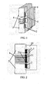
- a backplane 10 in a backplane 10, multiple connectors 2 connecting to a circuit board are disposed at one side of each vertical insertion plate 1, a part of the connectors (such as connectors 21 disposed at an upper end and a lower end) are used to install a service board 5, and a part of the connectors (such as connectors 22 disposed on the middle position) may be used to install a switch board 4.
- a service board 5 is connected to the connector 21 at two ends of a side of the vertical insertion plate 1 in a vertical insertion manner, and an installed service board 5 and the vertical insertion plate 1 are substantially in a coplanar or parallel state;
- the switch board 4 is connected to the connector 22, which is transversely disposed on the middle part of the vertical insertion plate 1, in a horizontal insertion manner, and an installed switch board 4 and the vertical insertion plate 1 are in an orthogonal state to each other; and the switch board 4 may be connected to one vertical insertion plate or connectors on the multiple vertical insertion plates that are transversely disposed.
- the backplane plane that is originally perpendicular to the service board is changed to be coplanar with or parallel to the service board, so that the service signal between the service board and the switch board that are connected by each connector is borne by one independent vertical insertion plate, and in this way, the original wiring space of one notch spacing of the backplane is expanded to the width of one vertical insertion plate, and the number of the layer of the vertical insertion plate may be lower than the number of the layer of the backplane, thereby solving the problem of processing bottleneck caused by the excessively large number of layers of a conventional backplane.
- multiple vertical insertion plates separately arranged from each other may be disposed in parallel, and a fixing component may be disposed (not shown in the figure), so that multiple vertical insertion plates are fixedly connected to form a backplane of an integral three-dimensional structure through the fixing component, so as to improve the convenience and stability of installation of the switch board and the service board in use.
- the fixing component may have a column structure or other structures, provided that the fixing component can be used to fixedly dispose multiple vertical insertion plates.
- each vertical insertion plate may serve as a plane bearing signal interconnection between the service board and the switch board, so that switching planes of both the service board and the switch board are distributed to wiring planes of multiple different vertical insertion plates, which greatly reduces the processing difficulty of the backplane and greatly reduces the cost, thus solving the problem of excessively large number of layers and excessively large size, which is caused by large-scale backplane wiring. Therefore, the backplane design and the switching capacity of the communication device are not limited by the processing capability of PCB, thereby ensuring the implementability of expansion of the communication device expansion in engineering.
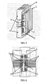
- the backplane provided by this embodiment is substantially the same as the backplane provided by Embodiment 1, the difference lies in that the backplane of this embodiment further includes a connecting plate 6 (referring to FIG. 3 ), so that multiple vertical insertion plates 1 separately arranged from each other are fixedly disposed on the connecting plate 6 and are fixedly connected through the connecting plate 6.
- a circuit for example, a printed circuit for supplying power to a switch board and/or a service board and/or controlling signal transmission is disposed on the connecting plate 6.
- the connecting plate 6 in the backplane may have the following structures.
- a connector for connecting the service board and/or the switch board is disposed on a surface of a connecting plate, the connector is electronically connected to a circuit (for example, a printed circuit) disposed on the plate body of the connecting plate, and through the connector and the printed circuit, power supply and/or signal transmission control for the service board and/or the switch board connected by the connector may be implemented.
- a notch for the connector on the vertical insertion plate to pass through is disposed on the plate body of the connecting plate, and the connector of each vertical insertion plate passes through the notch, so that multiple vertical insertion plates are fixed on the connecting plate.
- the connector of the connecting plate itself exists on a surface of the connecting plate, besides, the connector on the vertical insertion plate also exists on the surface of the connecting plate, so that the service board and the switch board may be connected to two connectors on the connecting plate respectively. Therefore, power supply and signal transmission control for the service board and the switch board can be implemented through the connecting plate, and service signal transmission between the service board and the switch board can be implemented through the vertical insertion plate.
- connectors are disposed at two surfaces of the connecting plate (the connectors on the two surfaces may be directly electronically connected through a through hole on the plate body, and may also be electronically connected through a circuit (for example, a printed circuit) on the plate body; the connector on one surface of the connecting plate is used to connect the service board and the switch board, and the connector on the other surface is used to interconnect with the connector on each vertical insertion plate, so that the multiple vertical insertion plates are fixedly connected to the connecting plate.
- a circuit for example, a printed circuit
- multiple vertical insertion plates may be fixed into an integral structure through the connecting plate, and therefore the alignment problem of the plates may be solved, the air flue may be changed, and the connecting plate may play a role in power supply transmission and signal control.
- the connecting plate may play a role in power supply transmission and signal control.
- the structure of a backplane provided by this embodiment is substantially the same as the structure provided by Embodiment 1, the difference lies in that, multiple connectors disposed on the backplane are respectively disposed at side edges of two opposite sides of the vertical insertion plate, that is, disposed at two opposite side edges of the vertical insertion plate.
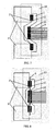
- backplanes of two structures may be formed, as shown in FIG. 4 , in a backplane 11 of a first structure, a connector 2 disposed at each side edge of the vertical insertion plate may connect a service board 5 and a switch board 4 respectively, the backplane of the three-dimensional structure can effectively improve the switching capacity at an equivalent volume.
- a backplane 12 of the other structure is shown in FIG. 5 , in which a connector disposed at one side edge of the vertical insertion plate 1 is used to install a service board 5, the installed service board 5 is coplanar with or parallel to a connected vertical insertion plate 1, and a connector 22 disposed at the other side edge of the vertical insertion plate 1 is used to install a switch board 4, the installed switch board 4 and the connected vertical insertion plate 1 are in an orthogonal state to each other.
- the service board and the switch board may be installed at the two sides, thereby avoiding the interference problem of connectors of a front board and a back board.
- two connecting plates 6 may also be disposed to form a backplane 13, and an installation connector for respectively installing a service board and/or a switch board is disposed on one side surface of each connecting plate, and the installation connector is electronically connected to a printed circuit disposed on the plate body of the connecting plate; the multiple vertical insertion plates are fixedly secured and connected between the two connecting plates and as for the connection manner between the vertical insertion plates and the two connecting plates, reference can be made to the description in Embodiment 2, which is not described here again.
- the two connecting plates may be common backplanes, and in the backplane of the three-dimensional structure, the service board and the switch board may be plugged in from two lateral sides, thereby ensuring the stability of the whole backplane, and avoiding the interference problem of connectors of a front board and a back board.
- a backplane 14 provided by this embodiment is substantially the same as the backplane of a second structure shown in FIG. 5 provided by Embodiment 3, the difference lies in that, as shown in FIG. 7 , in this backplane, each vertical insertion plate 1 is a shaped plate with a recessed central part, a connector 2 of an installation circuit board is respectively disposed at two ends of one side edge of the vertical insertion plate and a side edge of the recessed central part of the other side of the vertical insertion plate, and specifically, a service board 5 may be installed at a connector 21 disposed at the side edges of two end of one side of the vertical insertion plate, and a switch board 4 may be installed at a connector 22 disposed at the side edge of the recessed central part of the other side (referring to FIG. 7 ).
- the thickness of the backplane of this structure is small, therefore the overall volume after the service board and the switch board are installed is reduced, and the depth of a communication device is reduced.
- a connecting plate 6 is added on the basis of the backplane provided by Embodiment 5, so that multiple vertical insertion plates 1 separately arranged from each other are fixedly disposed on the connecting plate 6, and the multiple vertical insertion plates separately arranged from each other are fixedly connected through the connecting plate 6, and a circuit (for example, a printed circuit) for supplying power to the switch board and/or the service board and/or controlling signal transmission is disposed on the connecting plate 6.
- a circuit for example, a printed circuit
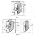
- the connecting plate 6 may adopts a common backplane, and a notch may be opened on the common backplane, so that the vertical insertion plates can be fixed on the connecting plate 6 through the notch on the connecting plate 6 to from a backplane of a three-dimensional structure shown in FIG. 8 .
- the stability of the backplane is improved, and power supply and control signal transmission can be conveniently implemented through installation of the connecting plate, and the overall volume after the service board and the switch board are installed is reduced.
- the device 30 includes: a switch board 4, a service board 5 and a backplane 31, where the switch board 4 and the service board 5 are connected to the backplane 31, signal interconnection is implemented through the backplane 31.
- the backplane 31 adopts the backplane of the three-dimensional structure provided by each foregoing embodiment.
- the communication device of this embodiment adopts the backplane of the three-dimensional structure as a switching plane of the switch board and the service board, the capacity of expansion of the communication device is not limited by the PCB process of the backplane, and the capacity of expansion of the communication device is improved.
- This embodiment provides a communication system, as shown in FIG. 10 .
- the system includes multiple communication devices 40, 50 in communication connection.
- Each of the communication devices 40 include: a switch board 4, a service board 5 and a backplane 41, where the switch board 4 and the service board 5 are connected to the backplane 41, and signal interconnection is implemented through the backplane 41.
- the backplane 41 in the communication device 40 adopts the backplane of the three-dimensional structure provided by each foregoing embodiment.
- each vertical insertion plate may serve as a plane bearing signal interconnection between the service board and the switch board, so that switching planes of both the service board and the switch board are distributed to wiring planes of multiple different vertical insertion plates, which greatly reduces the processing difficulty of the backplane and greatly reduces the cost, thus solving the problem of excessively large number of layers and excessively large size, which is caused by large-scale backplane wiring. Therefore, the backplane design and the switching capacity of the communication device are not limited by the processing capability of the PCB, thereby ensuring the implementability of expansion of the communication device expansion in engineering.
Landscapes
- Engineering & Computer Science (AREA)
- Computer Networks & Wireless Communication (AREA)
- Signal Processing (AREA)
- Mounting Of Printed Circuit Boards And The Like (AREA)
Claims (12)
- Rückwandplatine, die Folgendes umfasst:mehrere vertikale Einschubplatten (1), die getrennt voneinander angeordnet sind, wobei die vertikalen Einschubplatten mehrere Verbindungselemente (2) umfassen, die darauf angebracht sind, und Schaltungen (3), die als darauf gebildete Signalverdrahtung dienen, wobei die Verbindungselemente (2) mit den Schaltungen der vertikalen Einschubplatten (1), auf denen die Verbindungselemente (2) angebracht sind, elektronisch verbunden sind, um eine Signalverbindung zwischen Schaltplatinen (4) und Dienstplatinen (5) zu erreichen, wenn die Verbindungselemente auf den vertikalen Einschubplatten (1) die Schaltplatinen mit den Dienstplatinen verbinden;wobei dann, wenn die Verbindungselemente (2) auf den vertikalen Einschubplatten die Schaltplatinen (4) und die Dienstplatinen (5) verbinden, Verbindungselemente, die auf einer oder mehreren vertikalen Einschubplatten angebracht sind, mit den Schaltplatinen verbunden sind, und die vertikalen Einschubplatten (1) und die verbundenen Schaltplatinen (4) zueinander in einem orthogonalen Zustand sind; undwo die Verbindungselemente auf einer vertikalen Einschubplatte mit den Dienstplatinen (5) verbunden sind, und die vertikale Einschubplatte parallel mit oder komplanar zu den verbundenen Dienstplatinen ist.
- Rückwandplatine nach Anspruch 1, wobei die Verbindungselemente (2) auf der vertikalen Einschubplatte (1) Folgendes umfassen:mehrere Verbindungselemente (2), die an einer Seitenkante einer seitlichen Seite jeder der vertikalen Einschubplatten (1) angebracht sind.
- Rückwandplatine nach Anspruch 1, wobei die Verbindungselemente (2) auf der vertikalen Einschubplatte (1) Folgendes umfassen:mehrere Verbindungselemente (2), die an Seitenkanten von gegenüberliegenden seitlichen Seiten der vertikalen Einschubplatten angebracht sind.
- Rückwandplatine nach Anspruch 3, wobei die mehreren Verbindungselemente (2) an Seitenkanten von gegenüberliegenden Seiten der vertikalen Einschubplatten angebracht sind und Verbindungselemente zum Verbinden mit den Dienstplatinen an einer Seitenkante angebracht sind und Verbindungselemente zum Verbinden mit den Schaltplatinen an der anderen Seitenkante angebracht sind.
- Rückwandplatine nach Anspruch 1, wobei die mehreren vertikalen Einschubplatten (1), die getrennt voneinander angeordnet sind, parallel zueinander angebracht sind und durch eine Befestigungskomponente fest verbunden sind.
- Rückwandplatine nach Anspruch 1, die ferner Folgendes umfasst: Verbindungsplatten (6), wobei die mehreren vertikalen Einschubplatten (1), die getrennt voneinander angeordnet sind, durch die Verbindungsplatten fest verbunden sind, und Schaltungen zur Energieversorgung der Schaltplatinen (4) und/oder der Dienstplatinen (5) und/oder Steuersignalübertragung auf den Verbindungsplatten gebildet sind.
- Rückwandplatine nach Anspruch 6, wobei Verbindungselemente (2), die die Dienstplatinen (5) und/oder Schaltplatinen (4) verbinden, an einer Oberfläche der Verbindungsplatte (6) angebracht sind und die Verbindungselemente mit gedruckten Schaltungen, die auf Plattenkörpern der Verbindungsplatten gebildet sind, elektronisch verbunden sind; Aussparungen, die es erlauben, dass die Verbindungselemente auf der vertikalen Einschubplatte hindurchtreten, in den Plattenkörpern der Verbindungsplatten definiert sind und die Verbindungselemente jeder vertikalen Einschubplatte durch die Aussparungen hindurchtreten können, um die mehreren vertikalen Einschubplatten auf den Verbindungsplatten zu befestigen.
- Rückwandplatine nach Anspruch 6, wobei Verbindungselemente (2) an zwei Oberflächen jeder der Verbindungsplatten (6) angebracht sind und die Verbindungselemente auf den zwei Oberflächen jeder der Verbindungsplatten durch eine Schaltung, die auf dem Plattenkörper jeder der Verbindungsplatten angebracht ist, elektronisch verbunden sind; ein Verbindungselement auf einer Oberfläche jeder der Verbindungsplatten verwendet wird, um die Dienstplatine (5) und/oder die Schaltplatine (4) zu verbinden, und ein Verbindungselement auf der anderen Oberfläche konfiguriert ist, sich mit dem Verbindungselement auf jeder vertikalen Einschubplatte (1) zu verbinden, um die mehreren vertikalen Einschubplatten fest mit der Verbindungsplatte zu verbinden.
- Rückwandplatine nach Anspruch 7 oder 8, wobei zwei Verbindungsplatten (6) vorhanden sind und die mehreren vertikalen Einschubplatten (1), die getrennt voneinander angeordnet sind, zur Verbindung fest zwischen zwei Verbindungsplatten angebracht sind.
- Rückwandplatine nach Anspruch 1 oder 6, wobei jede vertikale Einschubplatte (1) eine geformte Platte mit einem ausgesparten mittleren Abschnitt ist, die Verbindungselemente (2) jeweils an Seitenkanten von zwei Enden einer Seite der vertikalen Einschubplatte und einer Seitenkante des ausgesparten mittleren Abschnitts der anderen Seite der vertikalen Einschubplatte angebracht sind, das Verbindungselement zum Verbinden mit der Dienstplatine an der Seitenkante von zwei Enden einer Seite der vertikalen Einschubplatte angebracht ist und das Verbindungselement zum Verbinden mit der Schaltplatine an einer Seitenkante des ausgesparten mittleren Abschnitts der anderen Seite angebracht ist.
- Kommunikationsvorrichtung, die Folgendes umfasst: wenigstens eine Schaltplatine (4), wenigstens eine Dienstplatine (5) und wenigstens eine Rückwandplatine (10), wobei die wenigstens eine Rückwandplatine die Rückwandplatine nach einem der Ansprüche 1 bis 10 ist, die wenigstens eine Schaltplatine und die wenigstens eine Dienstplatine mit der wenigstens einen Rückwandplatine verbunden sind und gegenseitige Signalverbindung über die wenigstens eine Rückwandplatine implementieren.
- Kommunikationsvorrichtung, die mehrere Kommunikationsvorrichtungen (40, 50) in Kommunikationsverbindung umfasst, wobei die Kommunikationsvorrichtung Folgendes umfasst: wenigstens eine Schaltplatine (4), wenigstens eine Dienstplatine (5) und wenigstens eine Rückwandplatine (10), wobei die wenigstens eine Rückwandplatine die Rückwandplatine oder die Rückwandplatinen nach einem der Ansprüche 1 bis 10 ist/sind, die wenigstens eine Schaltplatine und die wenigstens eine Dienstplatine mit der wenigstens einen Rückwandplatine verbunden sind und gegenseitige Signalverbindung über die wenigstens eine Rückwandplatine implementieren.
Applications Claiming Priority (2)
| Application Number | Priority Date | Filing Date | Title |
|---|---|---|---|
| CN2010105325444A CN101984599B (zh) | 2010-11-01 | 2010-11-01 | 背板及通讯设备、通讯系统 |
| PCT/CN2011/074692 WO2011137828A1 (zh) | 2010-11-01 | 2011-05-26 | 背板及通讯设备、通讯系统 |
Publications (3)
| Publication Number | Publication Date |
|---|---|
| EP2568537A1 EP2568537A1 (de) | 2013-03-13 |
| EP2568537A4 EP2568537A4 (de) | 2013-10-02 |
| EP2568537B1 true EP2568537B1 (de) | 2015-07-08 |
Family
ID=43641770
Family Applications (1)
| Application Number | Title | Priority Date | Filing Date |
|---|---|---|---|
| EP11777247.5A Active EP2568537B1 (de) | 2010-11-01 | 2011-05-26 | Rückseitenplatte, kommunikationsvorrichtung und kommunikationssystem |
Country Status (4)
| Country | Link |
|---|---|
| US (1) | US8861222B2 (de) |
| EP (1) | EP2568537B1 (de) |
| CN (1) | CN101984599B (de) |
| WO (1) | WO2011137828A1 (de) |
Families Citing this family (38)
| Publication number | Priority date | Publication date | Assignee | Title |
|---|---|---|---|---|
| CN101984599B (zh) | 2010-11-01 | 2013-09-11 | 华为技术有限公司 | 背板及通讯设备、通讯系统 |
| CN102645957B (zh) * | 2012-03-09 | 2014-05-07 | 华为技术有限公司 | 背板系统 |
| CN102681618A (zh) * | 2012-04-20 | 2012-09-19 | 华为技术有限公司 | 背板系统 |
| CN102946364B (zh) * | 2012-09-29 | 2015-12-02 | 华为技术有限公司 | 连接装置以及系统 |
| CN103780516B (zh) * | 2012-10-19 | 2017-06-09 | 华为技术有限公司 | 一种立体背板 |
| CN103813677A (zh) * | 2012-11-05 | 2014-05-21 | 华为技术有限公司 | 背板、机柜级通讯设备以及更换背板的方法 |
| CN103050800B (zh) * | 2012-12-25 | 2015-04-08 | 华为技术有限公司 | 电气连接装置及电子设备 |
| CN103051566B (zh) * | 2012-12-27 | 2015-12-23 | 华为技术有限公司 | 背板装置及通信设备 |
| CA2896779C (en) * | 2012-12-31 | 2017-10-03 | Huawei Technologies Co., Ltd. | Heat dissipation system for communications device |
| CN103974538B (zh) * | 2013-02-05 | 2017-09-12 | 华为技术有限公司 | 电子设备、电子系统及其电路板互联架构 |
| CN103236991B (zh) * | 2013-03-29 | 2016-08-24 | 华为技术有限公司 | 通信系统 |
| EP3068088A4 (de) * | 2013-12-04 | 2016-11-30 | Huawei Tech Co Ltd | Verbindungssystem für kommunikationsvorrichtung |
| CN104080308B (zh) * | 2014-06-20 | 2017-07-14 | 华为技术有限公司 | 背板及具有该背板的通讯设备 |
| US20160183402A1 (en) * | 2014-12-23 | 2016-06-23 | Intel Corporation | Reducing trace length and insertion loss of high speed signals on a network switch board |
| US9595798B2 (en) * | 2015-06-17 | 2017-03-14 | The Boeing Company | VME P2 five row interface adapter assembly, system, and method |
| CN106953816A (zh) * | 2016-01-06 | 2017-07-14 | 中兴通讯股份有限公司 | 通讯交换设备 |
| KR20170093596A (ko) * | 2016-02-05 | 2017-08-16 | 한국전자통신연구원 | 미드플레인 통신 시스템 |
| CN107124671B (zh) * | 2016-02-24 | 2022-01-25 | 中兴通讯股份有限公司 | 一种通信设备 |
| CN107154856A (zh) * | 2016-03-03 | 2017-09-12 | 中兴通讯股份有限公司 | 具有平行背板的通讯设备及其平行背板的布置方法 |
| CN107317770A (zh) * | 2016-04-27 | 2017-11-03 | 中兴通讯股份有限公司 | 背板装置、通信设备 |
| CN205670612U (zh) | 2016-06-15 | 2016-11-02 | 合肥京东方光电科技有限公司 | 一种电路转接装置 |
| CN108011214B (zh) * | 2016-10-31 | 2020-09-08 | 新华三技术有限公司 | 线缆背板系统及通信设备 |
| CN108270698B (zh) * | 2016-12-30 | 2021-12-14 | 中兴通讯股份有限公司 | 基于crossbar非正交架构的交换机背板互联装置及方法 |
| US10841246B2 (en) * | 2017-08-30 | 2020-11-17 | Arista Networks, Inc. | Distributed core switching with orthogonal fabric card and line cards |
| CN108170233B (zh) * | 2017-12-13 | 2019-11-19 | 浙江大华技术股份有限公司 | 一种机箱 |
| CN108134750B (zh) * | 2017-12-27 | 2021-06-29 | 迈普通信技术股份有限公司 | 一种背板及通信设备 |
| CN109996414A (zh) * | 2017-12-29 | 2019-07-09 | 中兴通讯股份有限公司 | 一种线缆背板、线缆盒和线缆组件 |
| US10680382B2 (en) * | 2018-08-27 | 2020-06-09 | Quanta Computer Inc. | Modular bridge array for bridging electronic components |
| CN109788697B (zh) | 2018-12-04 | 2021-04-09 | 华为技术有限公司 | 具有平行背板的电子设备及存储设备 |
| US10986423B2 (en) | 2019-04-11 | 2021-04-20 | Arista Networks, Inc. | Network device with compact chassis |
| CN111836121B (zh) * | 2019-04-18 | 2023-03-24 | 中兴通讯股份有限公司 | 一种板卡连接架构及具有该架构的通信设备 |
| CN210868472U (zh) * | 2019-07-17 | 2020-06-26 | 华为机器有限公司 | 框式设备 |
| US11266007B2 (en) | 2019-09-18 | 2022-03-01 | Arista Networks, Inc. | Linecard system using riser printed circuit boards (PCBS) |
| CN115939812A (zh) * | 2020-05-30 | 2023-04-07 | 华为技术有限公司 | 一种板级架构及通信设备 |
| CN111781992B (zh) | 2020-06-19 | 2022-03-08 | 苏州浪潮智能科技有限公司 | 一种服务器内多板卡的布局方法及服务器多板卡装置 |
| CN112462874A (zh) * | 2020-11-13 | 2021-03-09 | 苏州浪潮智能科技有限公司 | 一种服务器及其双维度模块热拔插结构 |
| WO2022268140A1 (zh) * | 2021-06-24 | 2022-12-29 | 广州市康珑电子有限公司 | 一种三维布线的电路板结构 |
| CN116133313B (zh) * | 2021-11-12 | 2025-06-13 | 华为技术有限公司 | 通信设备和业务信号调度的方法 |
Family Cites Families (13)
| Publication number | Priority date | Publication date | Assignee | Title |
|---|---|---|---|---|
| JP3698233B2 (ja) * | 1998-04-28 | 2005-09-21 | 富士通株式会社 | プリント配線板実装構造 |
| US6824393B2 (en) * | 2001-05-29 | 2004-11-30 | International Business Machines Corporation | Fragmented backplane system for I/O applications |
| US6757177B2 (en) | 2001-07-05 | 2004-06-29 | Tropic Networks Inc. | Stacked backplane assembly |
| JP2003037379A (ja) * | 2001-07-25 | 2003-02-07 | Toyo Commun Equip Co Ltd | プリント基板の接続構造 |
| US6918775B2 (en) | 2003-09-23 | 2005-07-19 | Hon Hai Precision Ind. Co., Ltd. | Method for interconnecting multiple printed circuit boards |
| TW200529497A (en) * | 2004-02-24 | 2005-09-01 | Hon Hai Prec Ind Co Ltd | Method for interconnecting multiple printed circuit boards |
| CN2735566Y (zh) | 2004-06-21 | 2005-10-19 | 中兴通讯股份有限公司南京分公司 | 一种子、母板间高速互联的结构 |
| US20070232089A1 (en) * | 2006-03-31 | 2007-10-04 | Nortel Networks Limited | Bridge modules for connecting plural groups of electronic modules |
| CN101001474A (zh) * | 2006-12-31 | 2007-07-18 | 华为技术有限公司 | 实现多种业务统一交换的通信设备、方法和交换板 |
| CN101299669A (zh) * | 2007-11-21 | 2008-11-05 | 华为技术有限公司 | 一种通信系统及装置 |
| CN101304543A (zh) * | 2008-06-17 | 2008-11-12 | 华为技术有限公司 | 双面插背板 |
| CN101931828B (zh) | 2009-06-12 | 2013-01-30 | 华为技术有限公司 | 背板和通讯设备 |
| CN101984599B (zh) | 2010-11-01 | 2013-09-11 | 华为技术有限公司 | 背板及通讯设备、通讯系统 |
-
2010
- 2010-11-01 CN CN2010105325444A patent/CN101984599B/zh active Active
-
2011
- 2011-05-26 EP EP11777247.5A patent/EP2568537B1/de active Active
- 2011-05-26 WO PCT/CN2011/074692 patent/WO2011137828A1/zh not_active Ceased
-
2012
- 2012-12-20 US US13/721,426 patent/US8861222B2/en active Active
Also Published As
| Publication number | Publication date |
|---|---|
| EP2568537A4 (de) | 2013-10-02 |
| US20130107489A1 (en) | 2013-05-02 |
| CN101984599A (zh) | 2011-03-09 |
| WO2011137828A1 (zh) | 2011-11-10 |
| CN101984599B (zh) | 2013-09-11 |
| EP2568537A1 (de) | 2013-03-13 |
| US8861222B2 (en) | 2014-10-14 |
Similar Documents
| Publication | Publication Date | Title |
|---|---|---|
| US8861222B2 (en) | Backplane, communication device and communication system | |
| EP2836058B1 (de) | Vertikales orthogonales verbindungssystem und kommunikationsvorrichtung | |
| US8267699B2 (en) | Backboard and communication device | |
| US7435095B1 (en) | Electrical interconnection system | |
| CN103503590B (zh) | 用于通信设备的散热系统 | |
| EP1955412A2 (de) | Monolithische platine mit einem ersten und einem zweiten teil | |
| WO2014146231A1 (zh) | 背板、插框和网络设备 | |
| CN101642006A (zh) | 用于配合具有不同宽度的板的底板 | |
| EP2830257B1 (de) | Atca-rückwandplatine | |
| CN102984881B (zh) | 电路板连接结构 | |
| EP1955170A2 (de) | Subrack mit vorder- und rückseitiger einfügung von amc-modulen | |
| CN104641593B (zh) | 网板和通信设备 | |
| EP3735116A1 (de) | Kabelrückwand, kabeldose und kabelanordnung | |
| CN104752851B (zh) | 一种系统 | |
| CN105027518B (zh) | 用于通信设备的互连系统 | |
| CN101841734B (zh) | 一种背板及背板通信系统 | |
| CN103098317B (zh) | 信号传输装置及电子设备 | |
| CN201946853U (zh) | 多插卡转接面板 | |
| CN203243353U (zh) | 一种背板 | |
| CN102665373B (zh) | 一种印刷电路板卡,及制造方法 | |
| JP3125446U (ja) | 高密度モジュール式コネクタ | |
| CN219592743U (zh) | 一种通信装置 | |
| CN105682352A (zh) | 背板系统、集中交换设备及背板连接和固定方法 | |
| WO2017067508A1 (zh) | 背板组件以及通信设备 | |
| KR20170093596A (ko) | 미드플레인 통신 시스템 |
Legal Events
| Date | Code | Title | Description |
|---|---|---|---|
| PUAI | Public reference made under article 153(3) epc to a published international application that has entered the european phase |
Free format text: ORIGINAL CODE: 0009012 |
|
| 17P | Request for examination filed |
Effective date: 20121205 |
|
| AK | Designated contracting states |
Kind code of ref document: A1 Designated state(s): AL AT BE BG CH CY CZ DE DK EE ES FI FR GB GR HR HU IE IS IT LI LT LU LV MC MK MT NL NO PL PT RO RS SE SI SK SM TR |
|
| A4 | Supplementary search report drawn up and despatched |
Effective date: 20130830 |
|
| RIC1 | Information provided on ipc code assigned before grant |
Ipc: H01R 12/51 20110101AFI20130826BHEP |
|
| DAX | Request for extension of the european patent (deleted) | ||
| GRAP | Despatch of communication of intention to grant a patent |
Free format text: ORIGINAL CODE: EPIDOSNIGR1 |
|
| INTG | Intention to grant announced |
Effective date: 20140708 |
|
| GRAS | Grant fee paid |
Free format text: ORIGINAL CODE: EPIDOSNIGR3 |
|
| GRAP | Despatch of communication of intention to grant a patent |
Free format text: ORIGINAL CODE: EPIDOSNIGR1 |
|
| INTG | Intention to grant announced |
Effective date: 20141217 |
|
| GRAA | (expected) grant |
Free format text: ORIGINAL CODE: 0009210 |
|
| AK | Designated contracting states |
Kind code of ref document: B1 Designated state(s): AL AT BE BG CH CY CZ DE DK EE ES FI FR GB GR HR HU IE IS IT LI LT LU LV MC MK MT NL NO PL PT RO RS SE SI SK SM TR |
|
| REG | Reference to a national code |
Ref country code: GB Ref legal event code: FG4D |
|
| REG | Reference to a national code |
Ref country code: AT Ref legal event code: REF Ref document number: 736030 Country of ref document: AT Kind code of ref document: T Effective date: 20150715 Ref country code: CH Ref legal event code: EP |
|
| REG | Reference to a national code |
Ref country code: IE Ref legal event code: FG4D |
|
| REG | Reference to a national code |
Ref country code: DE Ref legal event code: R096 Ref document number: 602011017740 Country of ref document: DE |
|
| REG | Reference to a national code |
Ref country code: AT Ref legal event code: MK05 Ref document number: 736030 Country of ref document: AT Kind code of ref document: T Effective date: 20150708 |
|
| REG | Reference to a national code |
Ref country code: NL Ref legal event code: MP Effective date: 20150708 |
|
| REG | Reference to a national code |
Ref country code: LT Ref legal event code: MG4D |
|
| PG25 | Lapsed in a contracting state [announced via postgrant information from national office to epo] |
Ref country code: LV Free format text: LAPSE BECAUSE OF FAILURE TO SUBMIT A TRANSLATION OF THE DESCRIPTION OR TO PAY THE FEE WITHIN THE PRESCRIBED TIME-LIMIT Effective date: 20150708 Ref country code: LT Free format text: LAPSE BECAUSE OF FAILURE TO SUBMIT A TRANSLATION OF THE DESCRIPTION OR TO PAY THE FEE WITHIN THE PRESCRIBED TIME-LIMIT Effective date: 20150708 Ref country code: NO Free format text: LAPSE BECAUSE OF FAILURE TO SUBMIT A TRANSLATION OF THE DESCRIPTION OR TO PAY THE FEE WITHIN THE PRESCRIBED TIME-LIMIT Effective date: 20151008 Ref country code: GR Free format text: LAPSE BECAUSE OF FAILURE TO SUBMIT A TRANSLATION OF THE DESCRIPTION OR TO PAY THE FEE WITHIN THE PRESCRIBED TIME-LIMIT Effective date: 20151009 Ref country code: FI Free format text: LAPSE BECAUSE OF FAILURE TO SUBMIT A TRANSLATION OF THE DESCRIPTION OR TO PAY THE FEE WITHIN THE PRESCRIBED TIME-LIMIT Effective date: 20150708 |
|
| PG25 | Lapsed in a contracting state [announced via postgrant information from national office to epo] |
Ref country code: AT Free format text: LAPSE BECAUSE OF FAILURE TO SUBMIT A TRANSLATION OF THE DESCRIPTION OR TO PAY THE FEE WITHIN THE PRESCRIBED TIME-LIMIT Effective date: 20150708 Ref country code: IS Free format text: LAPSE BECAUSE OF FAILURE TO SUBMIT A TRANSLATION OF THE DESCRIPTION OR TO PAY THE FEE WITHIN THE PRESCRIBED TIME-LIMIT Effective date: 20151108 Ref country code: PT Free format text: LAPSE BECAUSE OF FAILURE TO SUBMIT A TRANSLATION OF THE DESCRIPTION OR TO PAY THE FEE WITHIN THE PRESCRIBED TIME-LIMIT Effective date: 20151109 Ref country code: ES Free format text: LAPSE BECAUSE OF FAILURE TO SUBMIT A TRANSLATION OF THE DESCRIPTION OR TO PAY THE FEE WITHIN THE PRESCRIBED TIME-LIMIT Effective date: 20150708 Ref country code: SE Free format text: LAPSE BECAUSE OF FAILURE TO SUBMIT A TRANSLATION OF THE DESCRIPTION OR TO PAY THE FEE WITHIN THE PRESCRIBED TIME-LIMIT Effective date: 20150708 Ref country code: HR Free format text: LAPSE BECAUSE OF FAILURE TO SUBMIT A TRANSLATION OF THE DESCRIPTION OR TO PAY THE FEE WITHIN THE PRESCRIBED TIME-LIMIT Effective date: 20150708 Ref country code: RS Free format text: LAPSE BECAUSE OF FAILURE TO SUBMIT A TRANSLATION OF THE DESCRIPTION OR TO PAY THE FEE WITHIN THE PRESCRIBED TIME-LIMIT Effective date: 20150708 Ref country code: PL Free format text: LAPSE BECAUSE OF FAILURE TO SUBMIT A TRANSLATION OF THE DESCRIPTION OR TO PAY THE FEE WITHIN THE PRESCRIBED TIME-LIMIT Effective date: 20150708 |
|
| REG | Reference to a national code |
Ref country code: DE Ref legal event code: R097 Ref document number: 602011017740 Country of ref document: DE |
|
| REG | Reference to a national code |
Ref country code: FR Ref legal event code: PLFP Year of fee payment: 6 |
|
| PG25 | Lapsed in a contracting state [announced via postgrant information from national office to epo] |
Ref country code: SK Free format text: LAPSE BECAUSE OF FAILURE TO SUBMIT A TRANSLATION OF THE DESCRIPTION OR TO PAY THE FEE WITHIN THE PRESCRIBED TIME-LIMIT Effective date: 20150708 Ref country code: CZ Free format text: LAPSE BECAUSE OF FAILURE TO SUBMIT A TRANSLATION OF THE DESCRIPTION OR TO PAY THE FEE WITHIN THE PRESCRIBED TIME-LIMIT Effective date: 20150708 Ref country code: EE Free format text: LAPSE BECAUSE OF FAILURE TO SUBMIT A TRANSLATION OF THE DESCRIPTION OR TO PAY THE FEE WITHIN THE PRESCRIBED TIME-LIMIT Effective date: 20150708 Ref country code: DK Free format text: LAPSE BECAUSE OF FAILURE TO SUBMIT A TRANSLATION OF THE DESCRIPTION OR TO PAY THE FEE WITHIN THE PRESCRIBED TIME-LIMIT Effective date: 20150708 |
|
| PLBE | No opposition filed within time limit |
Free format text: ORIGINAL CODE: 0009261 |
|
| STAA | Information on the status of an ep patent application or granted ep patent |
Free format text: STATUS: NO OPPOSITION FILED WITHIN TIME LIMIT |
|
| PG25 | Lapsed in a contracting state [announced via postgrant information from national office to epo] |
Ref country code: RO Free format text: LAPSE BECAUSE OF FAILURE TO SUBMIT A TRANSLATION OF THE DESCRIPTION OR TO PAY THE FEE WITHIN THE PRESCRIBED TIME-LIMIT Effective date: 20150708 |
|
| 26N | No opposition filed |
Effective date: 20160411 |
|
| PG25 | Lapsed in a contracting state [announced via postgrant information from national office to epo] |
Ref country code: SI Free format text: LAPSE BECAUSE OF FAILURE TO SUBMIT A TRANSLATION OF THE DESCRIPTION OR TO PAY THE FEE WITHIN THE PRESCRIBED TIME-LIMIT Effective date: 20150708 Ref country code: BE Free format text: LAPSE BECAUSE OF NON-PAYMENT OF DUE FEES Effective date: 20160531 |
|
| PG25 | Lapsed in a contracting state [announced via postgrant information from national office to epo] |
Ref country code: BE Free format text: LAPSE BECAUSE OF FAILURE TO SUBMIT A TRANSLATION OF THE DESCRIPTION OR TO PAY THE FEE WITHIN THE PRESCRIBED TIME-LIMIT Effective date: 20150708 Ref country code: LU Free format text: LAPSE BECAUSE OF FAILURE TO SUBMIT A TRANSLATION OF THE DESCRIPTION OR TO PAY THE FEE WITHIN THE PRESCRIBED TIME-LIMIT Effective date: 20160526 |
|
| REG | Reference to a national code |
Ref country code: CH Ref legal event code: PL |
|
| PG25 | Lapsed in a contracting state [announced via postgrant information from national office to epo] |
Ref country code: LI Free format text: LAPSE BECAUSE OF NON-PAYMENT OF DUE FEES Effective date: 20160531 Ref country code: CH Free format text: LAPSE BECAUSE OF NON-PAYMENT OF DUE FEES Effective date: 20160531 |
|
| REG | Reference to a national code |
Ref country code: IE Ref legal event code: MM4A |
|
| REG | Reference to a national code |
Ref country code: FR Ref legal event code: PLFP Year of fee payment: 7 |
|
| PG25 | Lapsed in a contracting state [announced via postgrant information from national office to epo] |
Ref country code: IE Free format text: LAPSE BECAUSE OF NON-PAYMENT OF DUE FEES Effective date: 20160526 |
|
| PG25 | Lapsed in a contracting state [announced via postgrant information from national office to epo] |
Ref country code: NL Free format text: LAPSE BECAUSE OF FAILURE TO SUBMIT A TRANSLATION OF THE DESCRIPTION OR TO PAY THE FEE WITHIN THE PRESCRIBED TIME-LIMIT Effective date: 20150708 |
|
| REG | Reference to a national code |
Ref country code: FR Ref legal event code: PLFP Year of fee payment: 8 |
|
| PG25 | Lapsed in a contracting state [announced via postgrant information from national office to epo] |
Ref country code: CY Free format text: LAPSE BECAUSE OF FAILURE TO SUBMIT A TRANSLATION OF THE DESCRIPTION OR TO PAY THE FEE WITHIN THE PRESCRIBED TIME-LIMIT Effective date: 20150708 Ref country code: SM Free format text: LAPSE BECAUSE OF FAILURE TO SUBMIT A TRANSLATION OF THE DESCRIPTION OR TO PAY THE FEE WITHIN THE PRESCRIBED TIME-LIMIT Effective date: 20150708 Ref country code: HU Free format text: LAPSE BECAUSE OF FAILURE TO SUBMIT A TRANSLATION OF THE DESCRIPTION OR TO PAY THE FEE WITHIN THE PRESCRIBED TIME-LIMIT; INVALID AB INITIO Effective date: 20110526 |
|
| PG25 | Lapsed in a contracting state [announced via postgrant information from national office to epo] |
Ref country code: MT Free format text: LAPSE BECAUSE OF NON-PAYMENT OF DUE FEES Effective date: 20160531 Ref country code: TR Free format text: LAPSE BECAUSE OF FAILURE TO SUBMIT A TRANSLATION OF THE DESCRIPTION OR TO PAY THE FEE WITHIN THE PRESCRIBED TIME-LIMIT Effective date: 20150708 Ref country code: MK Free format text: LAPSE BECAUSE OF FAILURE TO SUBMIT A TRANSLATION OF THE DESCRIPTION OR TO PAY THE FEE WITHIN THE PRESCRIBED TIME-LIMIT Effective date: 20150708 Ref country code: MC Free format text: LAPSE BECAUSE OF FAILURE TO SUBMIT A TRANSLATION OF THE DESCRIPTION OR TO PAY THE FEE WITHIN THE PRESCRIBED TIME-LIMIT Effective date: 20150708 |
|
| PG25 | Lapsed in a contracting state [announced via postgrant information from national office to epo] |
Ref country code: BG Free format text: LAPSE BECAUSE OF FAILURE TO SUBMIT A TRANSLATION OF THE DESCRIPTION OR TO PAY THE FEE WITHIN THE PRESCRIBED TIME-LIMIT Effective date: 20150708 |
|
| PG25 | Lapsed in a contracting state [announced via postgrant information from national office to epo] |
Ref country code: AL Free format text: LAPSE BECAUSE OF FAILURE TO SUBMIT A TRANSLATION OF THE DESCRIPTION OR TO PAY THE FEE WITHIN THE PRESCRIBED TIME-LIMIT Effective date: 20150708 |
|
| REG | Reference to a national code |
Ref country code: FR Ref legal event code: PLFP Year of fee payment: 13 |
|
| P01 | Opt-out of the competence of the unified patent court (upc) registered |
Effective date: 20230524 |
|
| PGFP | Annual fee paid to national office [announced via postgrant information from national office to epo] |
Ref country code: DE Payment date: 20250402 Year of fee payment: 15 |
|
| PGFP | Annual fee paid to national office [announced via postgrant information from national office to epo] |
Ref country code: IT Payment date: 20250422 Year of fee payment: 15 |
|
| PGFP | Annual fee paid to national office [announced via postgrant information from national office to epo] |
Ref country code: FR Payment date: 20250401 Year of fee payment: 15 |
|
| PGFP | Annual fee paid to national office [announced via postgrant information from national office to epo] |
Ref country code: GB Payment date: 20260325 Year of fee payment: 16 |