EP2565930A2 - III-nitride semiconductor device - Google Patents
III-nitride semiconductor device Download PDFInfo
- Publication number
- EP2565930A2 EP2565930A2 EP12155007A EP12155007A EP2565930A2 EP 2565930 A2 EP2565930 A2 EP 2565930A2 EP 12155007 A EP12155007 A EP 12155007A EP 12155007 A EP12155007 A EP 12155007A EP 2565930 A2 EP2565930 A2 EP 2565930A2
- Authority
- EP
- European Patent Office
- Prior art keywords
- semiconductor
- layer
- layers
- semiconductor layer
- substrate
- Prior art date
- Legal status (The legal status is an assumption and is not a legal conclusion. Google has not performed a legal analysis and makes no representation as to the accuracy of the status listed.)
- Granted
Links
Images



Classifications
-
- H—ELECTRICITY
- H10—SEMICONDUCTOR DEVICES; ELECTRIC SOLID-STATE DEVICES NOT OTHERWISE PROVIDED FOR
- H10D—INORGANIC ELECTRIC SEMICONDUCTOR DEVICES
- H10D30/00—Field-effect transistors [FET]
- H10D30/40—FETs having zero-dimensional [0D], one-dimensional [1D] or two-dimensional [2D] charge carrier gas channels
- H10D30/47—FETs having zero-dimensional [0D], one-dimensional [1D] or two-dimensional [2D] charge carrier gas channels having two-dimensional [2D] charge carrier gas channels, e.g. nanoribbon FETs or high electron mobility transistors [HEMT]
- H10D30/471—High electron mobility transistors [HEMT] or high hole mobility transistors [HHMT]
- H10D30/475—High electron mobility transistors [HEMT] or high hole mobility transistors [HHMT] having wider bandgap layer formed on top of lower bandgap active layer, e.g. undoped barrier HEMTs such as i-AlGaN/GaN HEMTs
-
- H—ELECTRICITY
- H10—SEMICONDUCTOR DEVICES; ELECTRIC SOLID-STATE DEVICES NOT OTHERWISE PROVIDED FOR
- H10H—INORGANIC LIGHT-EMITTING SEMICONDUCTOR DEVICES HAVING POTENTIAL BARRIERS
- H10H20/00—Individual inorganic light-emitting semiconductor devices having potential barriers, e.g. light-emitting diodes [LED]
- H10H20/80—Constructional details
- H10H20/81—Bodies
- H10H20/816—Bodies having carrier transport control structures, e.g. highly-doped semiconductor layers or current-blocking structures
-
- H—ELECTRICITY
- H10—SEMICONDUCTOR DEVICES; ELECTRIC SOLID-STATE DEVICES NOT OTHERWISE PROVIDED FOR
- H10P—GENERIC PROCESSES OR APPARATUS FOR THE MANUFACTURE OR TREATMENT OF DEVICES COVERED BY CLASS H10
- H10P14/00—Formation of materials, e.g. in the shape of layers or pillars
- H10P14/20—Formation of materials, e.g. in the shape of layers or pillars of semiconductor materials
- H10P14/24—Formation of materials, e.g. in the shape of layers or pillars of semiconductor materials using chemical vapour deposition [CVD]
-
- H—ELECTRICITY
- H10—SEMICONDUCTOR DEVICES; ELECTRIC SOLID-STATE DEVICES NOT OTHERWISE PROVIDED FOR
- H10P—GENERIC PROCESSES OR APPARATUS FOR THE MANUFACTURE OR TREATMENT OF DEVICES COVERED BY CLASS H10
- H10P14/00—Formation of materials, e.g. in the shape of layers or pillars
- H10P14/20—Formation of materials, e.g. in the shape of layers or pillars of semiconductor materials
- H10P14/29—Formation of materials, e.g. in the shape of layers or pillars of semiconductor materials characterised by the substrates
- H10P14/2901—Materials
-
- H—ELECTRICITY
- H10—SEMICONDUCTOR DEVICES; ELECTRIC SOLID-STATE DEVICES NOT OTHERWISE PROVIDED FOR
- H10P—GENERIC PROCESSES OR APPARATUS FOR THE MANUFACTURE OR TREATMENT OF DEVICES COVERED BY CLASS H10
- H10P14/00—Formation of materials, e.g. in the shape of layers or pillars
- H10P14/20—Formation of materials, e.g. in the shape of layers or pillars of semiconductor materials
- H10P14/32—Formation of materials, e.g. in the shape of layers or pillars of semiconductor materials characterised by intermediate layers between substrates and deposited layers
- H10P14/3202—Materials thereof
- H10P14/3214—Materials thereof being Group IIIA-VA semiconductors
- H10P14/3216—Nitrides
-
- H—ELECTRICITY
- H10—SEMICONDUCTOR DEVICES; ELECTRIC SOLID-STATE DEVICES NOT OTHERWISE PROVIDED FOR
- H10P—GENERIC PROCESSES OR APPARATUS FOR THE MANUFACTURE OR TREATMENT OF DEVICES COVERED BY CLASS H10
- H10P14/00—Formation of materials, e.g. in the shape of layers or pillars
- H10P14/20—Formation of materials, e.g. in the shape of layers or pillars of semiconductor materials
- H10P14/32—Formation of materials, e.g. in the shape of layers or pillars of semiconductor materials characterised by intermediate layers between substrates and deposited layers
- H10P14/3242—Structure
- H10P14/3244—Layer structure
- H10P14/3248—Layer structure consisting of two layers
-
- H—ELECTRICITY
- H10—SEMICONDUCTOR DEVICES; ELECTRIC SOLID-STATE DEVICES NOT OTHERWISE PROVIDED FOR
- H10P—GENERIC PROCESSES OR APPARATUS FOR THE MANUFACTURE OR TREATMENT OF DEVICES COVERED BY CLASS H10
- H10P14/00—Formation of materials, e.g. in the shape of layers or pillars
- H10P14/20—Formation of materials, e.g. in the shape of layers or pillars of semiconductor materials
- H10P14/34—Deposited materials, e.g. layers
- H10P14/3402—Deposited materials, e.g. layers characterised by the chemical composition
- H10P14/3414—Deposited materials, e.g. layers characterised by the chemical composition being group IIIA-VIA materials
- H10P14/3416—Nitrides
-
- H—ELECTRICITY
- H10—SEMICONDUCTOR DEVICES; ELECTRIC SOLID-STATE DEVICES NOT OTHERWISE PROVIDED FOR
- H10P—GENERIC PROCESSES OR APPARATUS FOR THE MANUFACTURE OR TREATMENT OF DEVICES COVERED BY CLASS H10
- H10P14/00—Formation of materials, e.g. in the shape of layers or pillars
- H10P14/20—Formation of materials, e.g. in the shape of layers or pillars of semiconductor materials
- H10P14/34—Deposited materials, e.g. layers
- H10P14/3438—Doping during depositing
- H10P14/3441—Conductivity type
- H10P14/3442—N-type
-
- H—ELECTRICITY
- H10—SEMICONDUCTOR DEVICES; ELECTRIC SOLID-STATE DEVICES NOT OTHERWISE PROVIDED FOR
- H10P—GENERIC PROCESSES OR APPARATUS FOR THE MANUFACTURE OR TREATMENT OF DEVICES COVERED BY CLASS H10
- H10P14/00—Formation of materials, e.g. in the shape of layers or pillars
- H10P14/20—Formation of materials, e.g. in the shape of layers or pillars of semiconductor materials
- H10P14/34—Deposited materials, e.g. layers
- H10P14/3438—Doping during depositing
- H10P14/3441—Conductivity type
- H10P14/3444—P-type
-
- H—ELECTRICITY
- H10—SEMICONDUCTOR DEVICES; ELECTRIC SOLID-STATE DEVICES NOT OTHERWISE PROVIDED FOR
- H10D—INORGANIC ELECTRIC SEMICONDUCTOR DEVICES
- H10D62/00—Semiconductor bodies, or regions thereof, of devices having potential barriers
- H10D62/10—Shapes, relative sizes or dispositions of the regions of the semiconductor bodies; Shapes of the semiconductor bodies
- H10D62/17—Semiconductor regions connected to electrodes not carrying current to be rectified, amplified or switched, e.g. channel regions
- H10D62/351—Substrate regions of field-effect devices
- H10D62/357—Substrate regions of field-effect devices of FETs
-
- H—ELECTRICITY
- H10—SEMICONDUCTOR DEVICES; ELECTRIC SOLID-STATE DEVICES NOT OTHERWISE PROVIDED FOR
- H10D—INORGANIC ELECTRIC SEMICONDUCTOR DEVICES
- H10D62/00—Semiconductor bodies, or regions thereof, of devices having potential barriers
- H10D62/10—Shapes, relative sizes or dispositions of the regions of the semiconductor bodies; Shapes of the semiconductor bodies
- H10D62/17—Semiconductor regions connected to electrodes not carrying current to be rectified, amplified or switched, e.g. channel regions
- H10D62/351—Substrate regions of field-effect devices
- H10D62/357—Substrate regions of field-effect devices of FETs
- H10D62/364—Substrate regions of field-effect devices of FETs of IGFETs
- H10D62/371—Inactive supplementary semiconductor regions, e.g. for preventing punch-through, improving capacity effect or leakage current
-
- H—ELECTRICITY
- H10—SEMICONDUCTOR DEVICES; ELECTRIC SOLID-STATE DEVICES NOT OTHERWISE PROVIDED FOR
- H10D—INORGANIC ELECTRIC SEMICONDUCTOR DEVICES
- H10D62/00—Semiconductor bodies, or regions thereof, of devices having potential barriers
- H10D62/80—Semiconductor bodies, or regions thereof, of devices having potential barriers characterised by the materials
- H10D62/85—Semiconductor bodies, or regions thereof, of devices having potential barriers characterised by the materials being Group III-V materials, e.g. GaAs
- H10D62/8503—Nitride Group III-V materials, e.g. AlN or GaN
-
- H—ELECTRICITY
- H10—SEMICONDUCTOR DEVICES; ELECTRIC SOLID-STATE DEVICES NOT OTHERWISE PROVIDED FOR
- H10H—INORGANIC LIGHT-EMITTING SEMICONDUCTOR DEVICES HAVING POTENTIAL BARRIERS
- H10H20/00—Individual inorganic light-emitting semiconductor devices having potential barriers, e.g. light-emitting diodes [LED]
- H10H20/80—Constructional details
- H10H20/81—Bodies
- H10H20/822—Materials of the light-emitting regions
- H10H20/824—Materials of the light-emitting regions comprising only Group III-V materials, e.g. GaP
- H10H20/825—Materials of the light-emitting regions comprising only Group III-V materials, e.g. GaP containing nitrogen, e.g. GaN
Definitions
- Embodiments relate to a semiconductor device.
- the primary surface of the semiconductor substrate is exposed to source gas for forming the thin film while the semiconductor substrate is heated.
- the source gas may contain, for example, an organic metal compound of a Group III nitride semiconductor as a cation or may contain a Group V element as an anion.
- Vapor phase growth method is one form epitaxial crystal growth.
- a material of the thin film may be different from that of the substrate.
- the method of growing the thin film made of a material different from that of the substrate on the substrate is called a hetero epitaxial growth method.
- the thin film formed using the hetero epitaxial growth method is called a hetero epitaxial film, and an interface between the hetero epitaxial film and the substrate is called a hetero interface.
- the substrate refers to a member on which a target thin film is formed
- the substrate may comprise a single-layered substrate on a primary surface of which the target thin film is formed, and a substrate comprising one or more thin films previously formed thereon (a substrate on which an epitaxial film is previously formed and is defined as an epi-wafer).
- the target thin film is formed on the previously-formed thin film on the substrate.
- an InGaN thin film grown on a group III nitride semiconductor film such as a GaN crystal film may be problematic in that it is difficult to achieve a sharp gradient of an indium (In) concentration change near an interface between the InGaN film and the GaN film.
- the InGaN thin film having a desired indium concentration may not be formed on the GaN film.
- a transition layer having a lower indium (In) concentration may be formed up to approximately 1 to 2 nm in a direction of the thickness of the InGaN film from the interface between the InGaN and GaN films.
- Such a transition layer may prevent the indium concentration change nearby the interface between the InGaN film and GaN film from having a sharp gradient. This phenomenon may also occur when growing an AlGaN thin film on the GaN crystal film in the hetero epitaxial growth manner.
- the transition layer having such a lower or non-uniform indium concentration, formed near the interface using the hetero epitaxial growth method, may deteriorate characteristics of the semiconductor device employing the hetero epitaxial film. Therefore, in order to improve the characteristics of the semiconductor device employing the hetero epitaxial film, it is necessary to suppress the transition layer so that the sharp gradient of the concentration of the thin film near the hetero interface is achieved when using the hetero epitaxial growth method.
- spatially-relative terms such as “below”, “beneath”, “lower”, “above”, or “upper” may be used herein to describe one element's relationship to another element as illustrated in the figures. It will be understood that spatially-relative terms are intended to encompass different orientations of the device in addition to the orientations depicted in the figures. For example, if the device in one of the figures is turned over, elements described as “below” or “beneath” other elements would then be oriented “above” the other elements. The exemplary terms “below” or “beneath” can, therefore, encompass both an orientation of above and below. Since the device may be oriented in another direction, the spatially-relative terms may be interpreted in accordance with the orientation of the device.
- each layer is exaggerated, omitted, or schematically illustrated for convenience of description and clarity. Also, the size or area of each constituent element does not entirely reflect the actual size thereof.
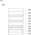
- FIG. 1 to FIG. 4 are cross-sectional views of structures of semiconductor devices 100 and 200 according to various exemplary embodiments.
- the semiconductor device 100 comprises a substrate 110, middle layers 140 and 150 comprising a first semiconductor layer 140 disposed on the substrate 110 and comprising Al x Ga 1-x N (0 ⁇ x ⁇ 1) doped with a first conduction type dopant and a second semiconductor layer 150 disposed on the first semiconductor layer 140 and comprising undoped gallium nitride (GaN), and a drive unit 160 disposed on the second semiconductor layer 150.
- the substrate 110 may be disposed under the first semiconductor layer 140.
- the substrate 110 may support the first semiconductor layer 140.
- the substrate 110 may receive heat from the first semiconductor layer 140.
- the material of the substrate 110 may be a semiconductor material, a metal material, a composite material or a combination thereof.
- the substrate 110 may be comprised the semiconductor material depending on implementation.
- the substrate 110 may be comprised a carrier wafer such as a silicon (Si), germanium (Ge), gallium arsenide (GaAs), zinc oxide (ZnO), silicon carbide (SiC), silicon germanium (SiGe), gallium nitride (GaN) or gallium (III) oxide (Ga 2 O 3 ) carrier wafer.
- a first buffer layer 120 is disposed on the substrate 110 and a second buffer layer 130 is disposed on the first buffer layer 120.
- the first and/or second buffer layers 120 and/or 130 may be comprised a material having a different lattice constant from that of the material of the substrate 110.
- the first and/or second buffer layers 120 and/or 130 may be comprised a material having a lattice constant characteristic similar to that of the material of the first and/or second semiconductor layers 140 and/or 150. For example, when the lattice constant of the material of the first and/or second semiconductor layers 140 and/or 150 is smaller than that of the material of the substrate 110, the lattice constant of the material of the first and/or second buffer layers 120 and/or 130 is smaller than that of the material of the substrate 110.
- the lattice constant of the material of the first and/or second semiconductor layers 140 and/or 150 is larger than that of the material of the substrate 110
- the lattice constant of the material of the first and/or second buffer layers 120 and/or 130 is larger than that of the material of the substrate 110.
- the first and/or second buffer layers 120 and/or 130 may have stress.
- the material of the first and/or second buffer layers 120 and/or 130 may have a smaller lattice constant than that of the material of the substrate 110.
- stress may occur at the first and/or second buffer layers 120 and/or 130, so that the first and/or second buffer layers 120 and/or 130 may be bent in a concave shape.
- the semiconductor device 100 may further comprise third and/or fourth buffer layers 172 and/or 174 interposed between the substrate 110 and the buffer layers 140 and 150.
- the fourth buffer 174 may be disposed on the third buffer layer 172.
- the third buffer layer 172 may comprise undoped Al x Ga 1-x N(0 ⁇ x ⁇ 1).
- the fourth buffer layer 174 may comprise undoped gallium nitride (GaN).
- the third and/or fourth buffer layers 172 and/or 174 need not be doped with a P type dopant and hence have an improved crystal characteristic. Thus, the third and/or fourth buffer layers 172 and/or 174 may improve crystal characteristics of the first and second semiconductor layers 140 and 150.
- the middle layers 140 and 150 may be disposed on the substrate 110. In another exemplary embodiment, the middle layers 140 and 150 may be disposed on the second buffer layer 130 or fourth buffer layer 174.
- the middle layers 140 and 150 may comprise the first semiconductor layer 140 and the second semiconductor layer 150 disposed on the first semiconductor layer 140.
- the first semiconductor layer 140 may be grown on the second buffer layer 130.
- the present disclosure is not limited thereto.
- the first semiconductor layer 140 may be comprised Al x Ga 1-x N(0 ⁇ x ⁇ 1).
- the first semiconductor layer 140 may be doped with a first dopant which may be a P type dopant.
- the first dopant may be magnesium (Mg), zinc (Zn), calcium (Ca), strontium (Sr), carbon (C), barium (Ba) or the like.
- the first semiconductor layer 140 may be doped with a P type dopant to contain holes therein.
- the first semiconductor layer 140 may be comprised gallium nitride (GaN) when x (a concentration of aluminum) is zero.
- GaN gallium nitride
- the first semiconductor layer 140 contains the holes, it may be possible to suppress current leakage resulting from a piezoelectric field effect occurring between the layers by the pressure generated due to differences in lattice constant between the substrate 110, the first buffer layer 120, the second buffer layer 130, the first semiconductor layer 140 and second semiconductor layer 150.
- the first semiconductor layer 140 contains the holes, it may be possible to prevent electrons from staying between the second buffer layer 130 and the second semiconductor layer 150. Accordingly, bending of an energy band between the first semiconductor layer 140 and second semiconductor layer 150 may be minimized and hence a piezoelectric field effect may be reduced.
- current leakage due to 2DEG (2 Dimensional electron gas) may be suppressed.
- the second semiconductor layer 150 may be disposed on the first semiconductor layer 140.
- the second semiconductor layer 150 may comprise undoped gallium nitride (GaN).
- the second semiconductor layer 150 may be formed by supplying NH 3 and trimethyl gallium (TMG) onto the second buffer layer 130 at 700 °C.
- TMG trimethyl gallium
- the present disclosure is not limited thereto.
- the second semiconductor layer 150 may be formed as an undoped layer having a predetermined thickness.
- the first and second semiconductor layers 140 and 150 have a stress like the first and/or second buffer layers 120 and/or 130.
- the first and second semiconductor layers 140 and 150 may exert the stress and hence may be bent in a convex shape. This stress may counteract the stress of the substrate 110, the first buffer layer 120 or the second buffer layer 130.
- the semiconductor device 100 may further comprise a third buffer layer 172 disposed between the substrate 110 and the middle layers 140 and 150 and comprising undoped Al x Ga 1 - x N (O ⁇ x ⁇ 1) and a fourth buffer layer 174 disposed between the third buffer layer 130 and the middle layers 140 and 150, and comprising undoped gallium nitride (GaN).
- a third buffer layer 172 disposed between the substrate 110 and the middle layers 140 and 150 and comprising undoped Al x Ga 1 - x N (O ⁇ x ⁇ 1) and a fourth buffer layer 174 disposed between the third buffer layer 130 and the middle layers 140 and 150, and comprising undoped gallium nitride (GaN).
- the third buffer layer 172 comprises undoped Al x Ga 1 - x N(0 ⁇ x ⁇ 1) to have an improved crystal characteristic.
- the third buffer layer 172 may be comprised gallium nitride (GaN) when x (a concentration of aluminum) is zero.
- the third and fourth buffer layers 172 and 174 are stacked on top of each other to minimize bending of the semiconductor layers. Thus, current leakage due to the 2DEG (2 Dimensional electron gas) may be suppressed.
- the first semiconductor layer 140 comprises a plurality of first semiconductor layers 140 and the second semiconductor layer 150 comprises a plurality of second semiconductor layers 150.
- the first and second semiconductor layers 140 and 150 are disposed to alternate with each other. As the alternating number of the first and second semiconductor layers 140 and 150 increases, the stress of the first and second semiconductor layers 140 and 150 increasingly counteracts the stress of the substrate 110, the first buffer layer 120 or the second buffer layer 130.
- first and/or second semiconductor layers 140 and/or 150 are grown at a slow growth rate, the first and/or second semiconductor layers 140 and/or 150 have an excellent crystal characteristic.
- first and/or second buffer layers 120 and/or 130 are grown at a slow growth rate, the first and/or second buffer layers 120 and/or 130 do not have an excellent crystal characteristic.
- the first and/or second semiconductor layers 140 and/or 150 may be formed using a different method than that used in forming the first and/or second buffer layers 120 and/or 130. The present disclosure is not limited thereto.
- the first and/or second semiconductor layers 140 and/or 150 may be formed using MOCVD (metal organic chemical vapor deposition), CVD (chemical vapor deposition), PECVD (plasma enhanced CVD), MBE (molecular beam epitaxy) or HVPE (hydride vapor phase epitaxy), etc.
- MOCVD metal organic chemical vapor deposition
- CVD chemical vapor deposition
- PECVD plasma enhanced CVD
- MBE molecular beam epitaxy
- HVPE hydrogen vapor phase epitaxy
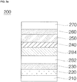
- the semiconductor device 200 comprises a substrate 210, middle layers 240, 250 and 260 comprising a first semiconductor layer 240 disposed on the substrate 210 and comprising Al x Ga 1-x N (0 ⁇ x ⁇ 1), a second semiconductor layer 250 disposed on the first semiconductor layer 240 and comprising undoped gallium nitride (GaN) and a third semiconductor layer 260 disposed on the second semiconductor layer 250 and doped with a first dopant, and a drive unit 270 disposed on the middle layers 240, 250 and 260.
- GaN undoped gallium nitride
- the substrate 210 may be disposed under the first, second and third semiconductor layers 240, 250 and 260 and may support the same.
- a first buffer layer 220 may be disposed on the substrate 210.
- a second buffer layer 230 may be disposed on the first buffer layer 220.
- the material or deposition method for forming the first and/or second buffer layers 220 and/or 230 may be the same as described above.
- the third buffer layer 282 may comprised undoped Al x Ga 1-x N (0 ⁇ x ⁇ 1).
- the fourth buffer layer 284 may comprise undoped gallium nitride (GaN).
- the first semiconductor layer 240 may be comprised Al x Ga 1-x N (0 ⁇ x ⁇ 1).
- the first semiconductor layer 240 according to one exemplary embodiment may be comprised undoped Al x Ga 1-x N (0 ⁇ x ⁇ 1). Even when the first semiconductor layer 240 is comprised the undoped layer, the first semiconductor layer 240 exerts the stress to reduce 2DEG (2 Dimensional electron gas) resulting from a piezoelectric field effect.
- the first semiconductor layer 240 may be doped with a first dopant which may be a P type dopant.
- the first dopant may be magnesium (Mg), zinc (Zn), calcium (Ca), strontium (Sr), carbon (C), barium (Ba) or the like.
- the first semiconductor layer 240 may be doped with a P type dopant to contain holes therein.
- a P type dopant to contain holes therein.
- the first semiconductor layer 240 contains holes, it may be possible to suppress current leakage resulting from a piezoelectric field effect occurring between the layers by the pressure generated due to differences in lattice constant between the substrate 210, the first buffer layer 220, the second buffer layer 230, the first semiconductor layer 240, and the second semiconductor layer 250.
- the first semiconductor layer 240 contains the holes, it may be possible to prevent electrons from remaining between the second buffer layer 230 and the second semiconductor layer 250.
- the second semiconductor layer 250 may be disposed on the first semiconductor layer 240.
- the second semiconductor layer 250 may comprise undoped gallium nitride (GaN). Since the first and second semiconductor layers 240 and 250 have a smaller lattice constant than that of the substrate 210, the first and second semiconductor layers 240 and 250 have a stress like the first and/or second buffer layers 220 and/or 230. The first and second semiconductor layers 240 and 250 may exert the stress and hence may be bent in a convex shape. This stress counteracts the stress of the substrate 210, the first buffer layer 220 or the second buffer layer 230. In this way, the stress applied to the second semiconductor layer 250 may be reduced.
- GaN undoped gallium nitride
- the third semiconductor layer 260 may be disposed on the second semiconductor layer 250.
- the third semiconductor layer 260 may comprise gallium nitride (GaN).
- the third semiconductor layer 260 may be doped with a first dopant which may be a P type dopant.
- the first dopant may be magnesium (Mg), zinc (Zn), calcium (Ca), strontium (Sr), carbon (C), barium (Ba) or the like.
- the third semiconductor layer 260 Since the third semiconductor layer 260 has a smaller lattice constant than that of the substrate 210, the third semiconductor layer 260 has a stress like the first and/or second buffer layers 220 and/or 230.
- the third semiconductor layer 260 may exert the stress and hence may be bent in a convex shape. This stress counteracts the stress of the substrate 210, the first buffer layer 220 or the second buffer layer 230.
- the third semiconductor layer 260 may minimize a P type doped region in the semiconductor device 200.
- the third semiconductor layer 260 may minimize a crystal quality deterioration of the nitride semiconductor resulting from the P type dopant.
- the third semiconductor layer 260 may be thinner than the second semiconductor layer 250.
- the third semiconductor layer 260 may contain holes therein.
- the first semiconductor layer 240 contains the holes, it may be possible to suppress current leakage resulting from a piezoelectric field effect occurring between the layers by the pressure generated due to differences in lattice constant between the substrate 210, the first buffer layer 220, the second buffer layer 230, the first semiconductor layer 240 and the second semiconductor layer 250.
- first, second and/or third semiconductor layers 240, 250 and 260 are grown at a slow growth rate, the first, second and/or third semiconductor layers 240, 250 and 260 have an excellent crystal characteristic.
- first and/or second buffer layers 220 and/or 230 are grown at a slow growth rate, the first and/or second buffer layers 220 and/or 230 do not have an excellent crystal characteristic.
- the first, second and/or third semiconductor layers 240, 250 and 260 may be formed using a different method than that used in forming the first and/or second buffer layers 220 and/or 230. The present disclosure is not limited thereto.
- the first, second and/or third semiconductor layers 240, 250 and 260 may be formed using MOCVD (metal organic chemical vapor deposition), CVD (chemical vapor deposition), PECVD (plasma enhanced CVD), MBE (molecular beam epitaxy) or HVPE (hydride vapor phase epitaxy), etc.
- MOCVD metal organic chemical vapor deposition
- CVD chemical vapor deposition
- PECVD plasma enhanced CVD
- MBE molecular beam epitaxy
- HVPE hydrogen vapor phase epitaxy
- FIG. 3B is a cross-sectional view of a semiconductor device 200 according to an exemplary embodiment different from that of FIG. 3A .
- the semiconductor device 200 may further comprise third and/or fourth buffer layers 286 and/or 288 interposed between the middle layers 240, 250 and 260 and a drive unit 270.
- the third buffer layer 286 may comprise undoped Al x Ga 1-x N(0 ⁇ x ⁇ 1). That is, the third buffer layer 286 having the same composition as the third buffer layer 282 disposed under the middle layers 240, 250 and 260 may be disposed over the middle layers 240, 250 and 260.
- the fourth buffer layer 288 may comprise undoped gallium nitride (GaN). That is, the fourth buffer layer 288 having the same composition as the fourth buffer layer 284 disposed under the middle layers 240, 250 and 260 may be disposed over the middle layers 240, 250 and 260.
- GaN undoped gallium nitride
- the third and/or fourth buffer layers 286 and/or 288 may not be doped with a P type dopant to have an excellent crystal characteristic. Thus, the third and/or fourth buffer layers 286 and/or 288 may improve crystal characteristics of the drive unit 270 disposed over the same.
- the first, second and third semiconductor layers 240, 250 and 260 may comprise a plurality of first, and second and third semiconductor layers respectively.
- the first, second and third semiconductor layers 240, 250 and 260 may be disposed to alternate with one another. As the alternating number of the first, second and third semiconductor layers 240, 250 and 260 increases, the stress of the first, second and third semiconductor layers 240, 250 and 260 increasingly counteracts the stress of the substrate 210, the first buffer layer 220 or the second buffer layer 230.
- FIG. 5 is a cross-sectional view of a structure of a drive unit 300 of a semiconductor device according to one exemplary embodiment.
- the drive unit 300 may comprise a light emitting structure 315 having a first conduction type semiconductor layer 320, a second conduction type semiconductor layer 340 and an active layer disposed between the first and second conduction type semiconductor layers 320 and 340.
- the light emitting structure 315 may be disposed over a middle layer 310.
- the present disclosure is not limited thereto.
- the middle layer 310 may be made of a material to allow lattice constants of the light emitting structure 315 and a layer disposed under the middle layer 310 to match each other.
- the active layer 330 may be disposed between the first and second conduction type semiconductor layers 320 and 340.
- One of the first and second conduction type semiconductor layers 320 and 340 may be implemented as a P type semiconductor layer doped with a P type dopant.
- the other of the first and second conduction type semiconductor layers 320 and 340 may be implemented as an N type semiconductor layer doped with an N type dopant.
- the second conduction type semiconductor layer 340 may be implemented as an N type semiconductor layer, and vice versa.
- the P type semiconductor layer may be comprised a semiconductor material having a composition of In x Al y Ga 1-x-y N (0 ⁇ x ⁇ 1, 0 ⁇ y ⁇ 1, and 0 ⁇ x+y ⁇ 1) such as gallium nitride (GaN), aluminum nitride (AlN), aluminum gallium nitride (AlGaN), indium gallium nitride (InGaN), indium nitride (InN), indium aluminum gallium nitride (InAlGaN), aluminum indium nitride (AlInN) or the like which is doped with a P type dopant such as magnesium (Mg), zinc (Zn), calcium (Ca), strontium (Sr), carbon (C), barium (Ba) or the like.
- a P type dopant such as magnesium (Mg), zinc (Zn), calcium (Ca), strontium (Sr), carbon (C), barium (Ba) or the like.
- the N type semiconductor layer may be comprised a semiconductor material having a composition of In x Al y Ga 1-x-y N (0 ⁇ x ⁇ 1, 0 ⁇ y ⁇ 1,and 0 ⁇ x+y ⁇ 1) such as gallium nitride (GaN), aluminum nitride (AlN), aluminum gallium nitride (AlGaN), indium gallium nitride (InGaN), indium nitride (InN), indium aluminum gallium nitride
- AlInN aluminum indium nitride
- AlInN aluminum indium nitride
- N type dopant such as silicon (Si), germanium (Ge), tin (Sn), selenium (Se), tellurium (Te), etc.
- the active layer 330 may be disposed between the first and second conduction type semiconductor layers 320 and 340.
- the active layer 330 may be a single or multiple quantum well structure, a quantum-wire structure, a quantum dot structure or the like using a Group III - Group V compound semiconductor material.
- the quantum well structure may be a single or multiple quantum well structure comprising a well layer having a composition of In x Al y Ga 1-x-y N (0 ⁇ x ⁇ 1, 0 ⁇ y ⁇ 1, and 0 ⁇ x+y ⁇ 1) and a barrier layer having a composition of In a Al b Ga 1-a-b N (0 ⁇ a ⁇ 1, 0 ⁇ b ⁇ 1, and 0 ⁇ a+b ⁇ 1).
- the well layer may be comprised a material having a smaller energy band gap than that of the barrier layer.
- an electrically conductive cladding layer (not shown) may be disposed on and/or beneath the active layer 330.
- the electrically conductive cladding layer (not shown) may be comprised an AlGaN based semiconductor material and may have a larger energy band gap than that of the active layer 330.
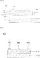
- FIG. 6 is a cross-sectional view of a structure of a drive unit 400 according to another exemplary embodiment.
- the drive unit 400 may comprise a first material layer 410, a second material layer 420 disposed on the first material layer 410 and supplying a channel, a source electrode 430 disposed on the second material layer 420, a gate electrode 440 disposed on the second material layer 420 and a drain electrode 450 disposed on the second material layer 420.
- the first material layer 410 may have smaller polarizability and energy band gap than those of the second material layer 420.
- the first material layer 410 may be a semiconductor layer.
- the first material layer 410 may comprised gallium nitride (GaN) or indium gallium nitride (InGaN). The present disclosure is not limited thereto.
- the second material layer 420 may be a semiconductor layer.
- the second material layer 420 may consist essentially of aluminum gallium nitride (AlGaN) or aluminum nitride (AIN). The present disclosure is not limited thereto.
- Charges of the second material layer 420 may be polarized charges. Charges occurring at an interface between the first and second material layers 410 and 420 may be 2 dimensional electron gas (2DEG).
- the second material layer 420 may be a channel supply layer to enable a 2DEG channel to be formed in the first material layer 410. In the second material layer 420, the 2 dimensional electron gas may counteract a surface charge resulting from the polarization.
- the first material layer 410 may be a channel formation layer.
- the source, gate and drain electrodes 430, 440 and 450 may be disposed on the second material layer 420.
- the source, gate and drain electrodes 430, 440 and 450 may be spaced from one another.
- the semiconductor device may comprise the middle layers.
- the current leakage due to a piezoelectric field effect may be suppressed.
- the drive unit may be reliably operated.
- a semiconductor device is not limited to the above-described exemplary embodiments in terms of configuration and manufacturing process. All or parts of each of the above-described exemplary embodiments may be selectively combined with each other such that a variety of medications may be made to the above-described exemplary embodiments.
Landscapes
- Junction Field-Effect Transistors (AREA)
- Led Devices (AREA)
Abstract
Description
- This application claims the priority benefit of Korean Patent Application No.
10-2011-0088647, filed on September 1, 2011 - Embodiments relate to a semiconductor device.
- When growing a thin film on a primary surface of a substrate, in particular, a semiconductor substrate to form a semiconductor device, the primary surface of the semiconductor substrate is exposed to source gas for forming the thin film while the semiconductor substrate is heated. The source gas may contain, for example, an organic metal compound of a Group III nitride semiconductor as a cation or may contain a Group V element as an anion. By supplying the source gas onto the primary surface of the semiconductor substrate, the thin film is grown on the primary surface of the semiconductor substrate.
- The above-mentioned method of growing the thin film is called a vapor phase growth method. Vapor phase growth method is one form epitaxial crystal growth. When growing a thin film on a substrate using the vapor phase growth method, for example, a material of the thin film may be different from that of the substrate. The method of growing the thin film made of a material different from that of the substrate on the substrate is called a hetero epitaxial growth method. Moreover, the thin film formed using the hetero epitaxial growth method is called a hetero epitaxial film, and an interface between the hetero epitaxial film and the substrate is called a hetero interface. As will be described later, the substrate refers to a member on which a target thin film is formed, and the substrate may comprise a single-layered substrate on a primary surface of which the target thin film is formed, and a substrate comprising one or more thin films previously formed thereon (a substrate on which an epitaxial film is previously formed and is defined as an epi-wafer). In the latter case, the target thin film is formed on the previously-formed thin film on the substrate.
- When forming the above mentioned hetero epitaxial film, for example, an InGaN thin film grown on a group III nitride semiconductor film such as a GaN crystal film may be problematic in that it is difficult to achieve a sharp gradient of an indium (In) concentration change near an interface between the InGaN film and the GaN film.
- To be specific, the InGaN thin film having a desired indium concentration may not be formed on the GaN film. For example, when forming the InGaN thin film having a thickness of approximately 5 nm, a transition layer having a lower indium (In) concentration may be formed up to approximately 1 to 2 nm in a direction of the thickness of the InGaN film from the interface between the InGaN and GaN films. Such a transition layer may prevent the indium concentration change nearby the interface between the InGaN film and GaN film from having a sharp gradient. This phenomenon may also occur when growing an AlGaN thin film on the GaN crystal film in the hetero epitaxial growth manner.
- The transition layer having such a lower or non-uniform indium concentration, formed near the interface using the hetero epitaxial growth method, may deteriorate characteristics of the semiconductor device employing the hetero epitaxial film. Therefore, in order to improve the characteristics of the semiconductor device employing the hetero epitaxial film, it is necessary to suppress the transition layer so that the sharp gradient of the concentration of the thin film near the hetero interface is achieved when using the hetero epitaxial growth method.
- One exemplary embodiment provides a semiconductor device comprising a substrate, middle layers comprising a first semiconductor layer disposed on the substrate and comprising AlxGa1-xN (0≤x≤1) doped with a first conduction type dopant and a second semiconductor layer disposed on the first semiconductor layer and comprising undoped gallium nitride (GaN), and a drive unit disposed on the second semiconductor layer.
- Details of the embodiments will be more clearly understood from the following detailed description taken in conjunction with the accompanying drawings, in which:
-
FIG. 1 is a cross-sectional view of a structure of a semiconductor device according to one exemplary embodiment; -
FIG. 2 is a cross-sectional view of a structure of a semiconductor device according to one exemplary embodiment; -
FIG. 3A is a cross-sectional view of a structure of a semiconductor device according to one exemplary embodiment; -
FIG. 3B is a cross-sectional view of a structure of a semiconductor device according to one exemplary embodiment; -
FIG. 4 is a cross-sectional view of a structure of a semiconductor device according to one exemplary embodiment; -
FIG. 5 is a cross-sectional view of a structure of a drive unit according to one exemplary embodiment; and -
FIG. 6 is a cross-sectional view of a structure of a drive unit according to one exemplary embodiment. - Reference will now be made in detail to embodiments, examples of which are illustrated in the accompanying drawings. However, the present disclosure may be embodied in many different forms and should not be construed as limited to the embodiments set forth herein. Rather, these embodiments are provided so that this disclosure will be thorough and complete, and will fully convey the scope of the disclosure to those skilled in the art. The present disclosure is defined only by the categories of the claims. In certain embodiments, detailed descriptions of device constructions or processes well known in the art may be omitted to avoid obscuring the disclosure by a person of ordinary skill in the art. Wherever possible, the same reference numbers will be used throughout the drawings to refer to the same or like parts.
- Spatially-relative terms such as "below", "beneath", "lower", "above", or "upper" may be used herein to describe one element's relationship to another element as illustrated in the figures. It will be understood that spatially-relative terms are intended to encompass different orientations of the device in addition to the orientations depicted in the figures. For example, if the device in one of the figures is turned over, elements described as "below" or "beneath" other elements would then be oriented "above" the other elements. The exemplary terms "below" or "beneath" can, therefore, encompass both an orientation of above and below. Since the device may be oriented in another direction, the spatially-relative terms may be interpreted in accordance with the orientation of the device.
- The terminology used in the present disclosure is for the purpose of describing particular embodiments only and is not intended to limit the disclosure. As used in the disclosure and the appended claims, the singular forms "a", "an" and "the" are intended to comprise the plural forms as well, unless context clearly indicates otherwise. It will be further understood that the terms "comprises" and/or "comprising," when used in this specification, specify the presence of stated features, integers, steps, operations, elements, and/or components, but do not preclude the presence or addition of one or more other features, integers, steps, operations, elements, components, and/or groups thereof.
- Unless otherwise defined, all terms (comprising technical and scientific terms) used herein have the same meaning as commonly understood by one of ordinary skill in the art. It will be further understood that terms, such as those defined in commonly used dictionaries, should be interpreted as having a meaning that is consistent with their meaning in the context of the relevant art and the present disclosure, and will not be interpreted in an idealized or overly formal sense unless expressly so defined herein.
- In the drawings, the thickness or size of each layer is exaggerated, omitted, or schematically illustrated for convenience of description and clarity. Also, the size or area of each constituent element does not entirely reflect the actual size thereof.
- Hereinafter, embodiments will be described in detail with reference to the drawings.
-
FIG. 1 to FIG. 4 are cross-sectional views of structures ofsemiconductor devices - Referring to
FIG. 1 , there is illustrated asemiconductor device 100 according to one exemplary embodiment. Thesemiconductor device 100 comprises asubstrate 110,middle layers first semiconductor layer 140 disposed on thesubstrate 110 and comprising AlxGa1-xN (0≤x≤1) doped with a first conduction type dopant and asecond semiconductor layer 150 disposed on thefirst semiconductor layer 140 and comprising undoped gallium nitride (GaN), and adrive unit 160 disposed on thesecond semiconductor layer 150. - The
substrate 110 may be disposed under thefirst semiconductor layer 140. Thesubstrate 110 may support thefirst semiconductor layer 140. Thesubstrate 110 may receive heat from thefirst semiconductor layer 140. - The material of the
substrate 110 may be a semiconductor material, a metal material, a composite material or a combination thereof. Thesubstrate 110 may be comprised the semiconductor material depending on implementation. For example, thesubstrate 110 may be comprised a carrier wafer such as a silicon (Si), germanium (Ge), gallium arsenide (GaAs), zinc oxide (ZnO), silicon carbide (SiC), silicon germanium (SiGe), gallium nitride (GaN) or gallium (III) oxide (Ga2O3) carrier wafer. - The
substrate 110 may be comprised an electrically conductive material. Thesubstrate 110 may be comprised a metal material according to implementation. For example, thesubstrate 110 may be comprised any one selected from a group consisting of gold (Au), nickel (Ni), tungsten (W), molybdenum (Mo), copper (Cu), aluminum (Al), tantalum (Ta), silver (Ag), platinum (Pt), chromium (Cr) and an alloy thereof. Thesubstrate 110 may be formed in a stack of two or more layers made of the above-described metal elements respectively. - A
first buffer layer 120 is disposed on thesubstrate 110 and asecond buffer layer 130 is disposed on thefirst buffer layer 120. The first and/or second buffer layers 120 and/or 130 may be comprised a material having a different lattice constant from that of the material of thesubstrate 110. The first and/or second buffer layers 120 and/or 130 may be comprised a material having a lattice constant characteristic similar to that of the material of the first and/or second semiconductor layers 140 and/or 150. For example, when the lattice constant of the material of the first and/or second semiconductor layers 140 and/or 150 is smaller than that of the material of thesubstrate 110, the lattice constant of the material of the first and/or second buffer layers 120 and/or 130 is smaller than that of the material of thesubstrate 110. When the lattice constant of the material of the first and/or second semiconductor layers 140 and/or 150 is larger than that of the material of thesubstrate 110, the lattice constant of the material of the first and/or second buffer layers 120 and/or 130 is larger than that of the material of thesubstrate 110. The first and/or second buffer layers 120 and/or 130 may have stress. - The
first buffer layer 120 may be of aluminum nitride (AIN). Source gas for forming thefirst buffer layer 120 may contain aluminum (AI), trimethyl aluminum (TMA), triethyl aluminum (TEA), trimethylamine aluminum (TMMA), dimethylethylamine aluminum (DMEAA), triisobutyl aluminum (TIBA), etc., and reaction gas may contain ammonia (NH3). The source and reaction gases are introduced to a reaction chamber and react with each other at 500 to 600 °C to form thefirst buffer layer 120. The present disclosure is not limited thereto. - The
second buffer layer 130 may be comprised aluminum gallium nitride (AlGaN). The first and/or second buffer layers 120 and/or 130 may be grown in a single-crystal form on thesubstrate 110. The present disclosure is not limited thereto. - The first and/or second buffer layers 120 and/or 130 may reduce lattice mismatching between the
substrate 110 and thefirst semiconductor layer 140. The first and/or second buffer layers 120 and/or 130 may enable thefirst semiconductor layer 140 to be easily grown thereon. The first and/or second buffer layers 120 and/or 130 may improve crystal characteristics of thefirst semiconductor layer 140. The first and/or second buffer layers 120 and/or 130 may be comprised a material to reduce a difference in lattice constant between thesubstrate 110 and thefirst semiconductor layer 140. - In the
semiconductor device 100 according to one exemplary embodiment, the material of the first and/or second buffer layers 120 and/or 130 may have a smaller lattice constant than that of the material of thesubstrate 110. When the first and/or second buffer layers 120 and/or 130 having a smaller lattice constant than that of thesubstrate 110 is disposed on thesubstrate 110, stress may occur at the first and/or second buffer layers 120 and/or 130, so that the first and/or second buffer layers 120 and/or 130 may be bent in a concave shape. - Although the first and/or second buffer layers 120 and/or 130 may be comprised the nitride material, the first and/or second buffer layers 120 and/or 130 may be formed using a different method than that used in forming the first and/or second semiconductor layers 140 and/or 150. The present disclosure is not limited thereto. In some cases, the first and/or second buffer layers 120 and/or 130 may be formed using MOCVD. Alternatively, the first and/or second buffer layers 120 and/or 130 may be rapidly disposed on the
substrate 110 using sputtering or HVPE. - The
semiconductor device 100 may further comprise third and/or fourth buffer layers 172 and/or 174 interposed between thesubstrate 110 and the buffer layers 140 and 150. Thefourth buffer 174 may be disposed on thethird buffer layer 172. - The
third buffer layer 172 may comprise undoped AlxGa1-xN(0≤x≤1). Thefourth buffer layer 174 may comprise undoped gallium nitride (GaN). - The third and/or fourth buffer layers 172 and/or 174 need not be doped with a P type dopant and hence have an improved crystal characteristic. Thus, the third and/or fourth buffer layers 172 and/or 174 may improve crystal characteristics of the first and second semiconductor layers 140 and 150.
- The
middle layers substrate 110. In another exemplary embodiment, themiddle layers second buffer layer 130 orfourth buffer layer 174. - The
middle layers first semiconductor layer 140 and thesecond semiconductor layer 150 disposed on thefirst semiconductor layer 140. Thefirst semiconductor layer 140 may be grown on thesecond buffer layer 130. The present disclosure is not limited thereto. - The
first semiconductor layer 140 may be comprised AlxGa1-xN(0≤x≤1). Thefirst semiconductor layer 140 may be doped with a first dopant which may be a P type dopant. The first dopant may be magnesium (Mg), zinc (Zn), calcium (Ca), strontium (Sr), carbon (C), barium (Ba) or the like. - The
first semiconductor layer 140 may be doped with a P type dopant to contain holes therein. Thefirst semiconductor layer 140 may be comprised gallium nitride (GaN) when x (a concentration of aluminum) is zero. When thefirst semiconductor layer 140 contains the holes, it may be possible to suppress current leakage resulting from a piezoelectric field effect occurring between the layers by the pressure generated due to differences in lattice constant between thesubstrate 110, thefirst buffer layer 120, thesecond buffer layer 130, thefirst semiconductor layer 140 andsecond semiconductor layer 150. When thefirst semiconductor layer 140 contains the holes, it may be possible to prevent electrons from staying between thesecond buffer layer 130 and thesecond semiconductor layer 150. Accordingly, bending of an energy band between thefirst semiconductor layer 140 andsecond semiconductor layer 150 may be minimized and hence a piezoelectric field effect may be reduced. Thus, current leakage due to 2DEG (2 Dimensional electron gas) may be suppressed. - The
second semiconductor layer 150 may be disposed on thefirst semiconductor layer 140. Thesecond semiconductor layer 150 may comprise undoped gallium nitride (GaN). For example, thesecond semiconductor layer 150 may be formed by supplying NH3 and trimethyl gallium (TMG) onto thesecond buffer layer 130 at 700 °C. The present disclosure is not limited thereto. Thesecond semiconductor layer 150 may be formed as an undoped layer having a predetermined thickness. - Since the first and second semiconductor layers 140 and 150 have a smaller lattice constant than that of the
substrate 110, the first and second semiconductor layers 140 and 150 have a stress like the first and/or second buffer layers 120 and/or 130. The first and second semiconductor layers 140 and 150 may exert the stress and hence may be bent in a convex shape. This stress may counteract the stress of thesubstrate 110, thefirst buffer layer 120 or thesecond buffer layer 130. - Since bending of the first and second semiconductor layers 140 and 150 is minimized, the
semiconductor device 100 has a uniform concentration of aluminum. - Referring to
FIG. 1 , thesemiconductor device 100 may further comprise athird buffer layer 172 disposed between thesubstrate 110 and themiddle layers fourth buffer layer 174 disposed between thethird buffer layer 130 and themiddle layers - The
third buffer layer 172 comprises undoped AlxGa1-xN(0≤x≤1) to have an improved crystal characteristic. Thethird buffer layer 172 may be comprised gallium nitride (GaN) when x (a concentration of aluminum) is zero. The third and fourth buffer layers 172 and 174 are stacked on top of each other to minimize bending of the semiconductor layers. Thus, current leakage due to the 2DEG (2 Dimensional electron gas) may be suppressed. - Referring to
FIG. 2 , thefirst semiconductor layer 140 comprises a plurality of first semiconductor layers 140 and thesecond semiconductor layer 150 comprises a plurality of second semiconductor layers 150. The first and second semiconductor layers 140 and 150 are disposed to alternate with each other. As the alternating number of the first and second semiconductor layers 140 and 150 increases, the stress of the first and second semiconductor layers 140 and 150 increasingly counteracts the stress of thesubstrate 110, thefirst buffer layer 120 or thesecond buffer layer 130. - Although the first and/or second semiconductor layers 140 and/or 150 are grown at a slow growth rate, the first and/or second semiconductor layers 140 and/or 150 have an excellent crystal characteristic. On the other hand, when the first and/or second buffer layers 120 and/or 130 are grown at a slow growth rate, the first and/or second buffer layers 120 and/or 130 do not have an excellent crystal characteristic. The first and/or second semiconductor layers 140 and/or 150 may be formed using a different method than that used in forming the first and/or second buffer layers 120 and/or 130. The present disclosure is not limited thereto.
- For example, the first and/or second semiconductor layers 140 and/or 150 may be formed using MOCVD (metal organic chemical vapor deposition), CVD (chemical vapor deposition), PECVD (plasma enhanced CVD), MBE (molecular beam epitaxy) or HVPE (hydride vapor phase epitaxy), etc. The present disclosure is not limited thereto.
- Referring to
FIG. 3A , there is illustrated asemiconductor device 200 according to one exemplary embodiment. Thesemiconductor device 200 comprises asubstrate 210,middle layers first semiconductor layer 240 disposed on thesubstrate 210 and comprising AlxGa1-xN (0≤x≤1), asecond semiconductor layer 250 disposed on thefirst semiconductor layer 240 and comprising undoped gallium nitride (GaN) and athird semiconductor layer 260 disposed on thesecond semiconductor layer 250 and doped with a first dopant, and adrive unit 270 disposed on themiddle layers - The same descriptions as in
FIG. 1 andFIG. 2 may be omitted hereinafter. - The
substrate 210 may be disposed under the first, second and third semiconductor layers 240, 250 and 260 and may support the same. - On the
substrate 210, afirst buffer layer 220 may be disposed. On thefirst buffer layer 220, asecond buffer layer 230 may be disposed. The material or deposition method for forming the first and/or second buffer layers 220 and/or 230 may be the same as described above. - The
semiconductor device 200 may further comprise third and/or fourth buffer layers 282 and/or 284 interposed between thesubstrate 210 and themiddle layers fourth buffer layer 284 may be formed on thethird buffer layer 282. - The
third buffer layer 282 may comprised undoped AlxGa1-xN (0≤x≤1). Thefourth buffer layer 284 may comprise undoped gallium nitride (GaN). - The third and/or fourth buffer layers 282 and/or 284 may not be doped with a P type dopant to have excellent crystal characteristic. Thus, the third and/or fourth buffer layers 282 and/or 284 may improve crystal characteristics of the first, second and third semiconductor layers 240, 250 and 260 thereon.
- The
first semiconductor layer 240 may be comprised AlxGa1-xN (0≤x≤1). Thefirst semiconductor layer 240 according to one exemplary embodiment may be comprised undoped AlxGa1-xN (0≤x≤1). Even when thefirst semiconductor layer 240 is comprised the undoped layer, thefirst semiconductor layer 240 exerts the stress to reduce 2DEG (2 Dimensional electron gas) resulting from a piezoelectric field effect. - The
first semiconductor layer 240 according to another exemplary embodiment may be doped with a first dopant which may be a P type dopant. The first dopant may be magnesium (Mg), zinc (Zn), calcium (Ca), strontium (Sr), carbon (C), barium (Ba) or the like. - The
first semiconductor layer 240 may be doped with a P type dopant to contain holes therein. When thefirst semiconductor layer 240 contains holes, it may be possible to suppress current leakage resulting from a piezoelectric field effect occurring between the layers by the pressure generated due to differences in lattice constant between thesubstrate 210, thefirst buffer layer 220, thesecond buffer layer 230, thefirst semiconductor layer 240, and thesecond semiconductor layer 250. When thefirst semiconductor layer 240 contains the holes, it may be possible to prevent electrons from remaining between thesecond buffer layer 230 and thesecond semiconductor layer 250. - The
second semiconductor layer 250 may be disposed on thefirst semiconductor layer 240. Thesecond semiconductor layer 250 may comprise undoped gallium nitride (GaN). Since the first and second semiconductor layers 240 and 250 have a smaller lattice constant than that of thesubstrate 210, the first and second semiconductor layers 240 and 250 have a stress like the first and/or second buffer layers 220 and/or 230. The first and second semiconductor layers 240 and 250 may exert the stress and hence may be bent in a convex shape. This stress counteracts the stress of thesubstrate 210, thefirst buffer layer 220 or thesecond buffer layer 230. In this way, the stress applied to thesecond semiconductor layer 250 may be reduced. - The
third semiconductor layer 260 may be disposed on thesecond semiconductor layer 250. Thethird semiconductor layer 260 may comprise gallium nitride (GaN). Thethird semiconductor layer 260 may be doped with a first dopant which may be a P type dopant. The first dopant may be magnesium (Mg), zinc (Zn), calcium (Ca), strontium (Sr), carbon (C), barium (Ba) or the like. - Since the
third semiconductor layer 260 has a smaller lattice constant than that of thesubstrate 210, thethird semiconductor layer 260 has a stress like the first and/or second buffer layers 220 and/or 230. Thethird semiconductor layer 260 may exert the stress and hence may be bent in a convex shape. This stress counteracts the stress of thesubstrate 210, thefirst buffer layer 220 or thesecond buffer layer 230. - The
third semiconductor layer 260 may minimize a P type doped region in thesemiconductor device 200. Thus, thethird semiconductor layer 260 may minimize a crystal quality deterioration of the nitride semiconductor resulting from the P type dopant. Thethird semiconductor layer 260 may be thinner than thesecond semiconductor layer 250. - The
third semiconductor layer 260 may have a thickness in a range of 10 to 100 nm. When thethird semiconductor layer 260 has a thickness below 10 nm, 2DEG (2 Dimensional electron gas) compensation effects cannot be obtained. When thethird semiconductor layer 260 has a thickness above 100 nm, the crystal characteristics thereof may be adversely affected. - The
third semiconductor layer 260 may contain holes therein. When thefirst semiconductor layer 240 contains the holes, it may be possible to suppress current leakage resulting from a piezoelectric field effect occurring between the layers by the pressure generated due to differences in lattice constant between thesubstrate 210, thefirst buffer layer 220, thesecond buffer layer 230, thefirst semiconductor layer 240 and thesecond semiconductor layer 250. - In the
semiconductor device 200 according to one exemplary embodiment, bending of the semiconductor device may be minimized due to counteraction between the stresses of the layers. As the bending of thesemiconductor device 200 is minimized, the concentration across the entire area of each semiconductor layer may be uniform. - Although the first, second and/or third semiconductor layers 240, 250 and 260 are grown at a slow growth rate, the first, second and/or third semiconductor layers 240, 250 and 260 have an excellent crystal characteristic. On the other hand, when the first and/or second buffer layers 220 and/or 230 are grown at a slow growth rate, the first and/or second buffer layers 220 and/or 230 do not have an excellent crystal characteristic. The first, second and/or third semiconductor layers 240, 250 and 260 may be formed using a different method than that used in forming the first and/or second buffer layers 220 and/or 230. The present disclosure is not limited thereto.
- For example, the first, second and/or third semiconductor layers 240, 250 and 260 may be formed using MOCVD (metal organic chemical vapor deposition), CVD (chemical vapor deposition), PECVD (plasma enhanced CVD), MBE (molecular beam epitaxy) or HVPE (hydride vapor phase epitaxy), etc. The present disclosure is not limited thereto.
-
FIG. 3B is a cross-sectional view of asemiconductor device 200 according to an exemplary embodiment different from that ofFIG. 3A . - Referring to
FIG. 3B , thesemiconductor device 200 may further comprise third and/or fourth buffer layers 286 and/or 288 interposed between themiddle layers drive unit 270. - The
third buffer layer 286 may comprise undoped AlxGa1-xN(0≤x≤1). That is, thethird buffer layer 286 having the same composition as thethird buffer layer 282 disposed under themiddle layers middle layers - The
fourth buffer layer 288 may comprise undoped gallium nitride (GaN). That is, thefourth buffer layer 288 having the same composition as thefourth buffer layer 284 disposed under themiddle layers middle layers - The third and/or fourth buffer layers 286 and/or 288 may not be doped with a P type dopant to have an excellent crystal characteristic. Thus, the third and/or fourth buffer layers 286 and/or 288 may improve crystal characteristics of the
drive unit 270 disposed over the same. - Referring to
FIG. 4 , the first, second and third semiconductor layers 240, 250 and 260 may comprise a plurality of first, and second and third semiconductor layers respectively. The first, second and third semiconductor layers 240, 250 and 260 may be disposed to alternate with one another. As the alternating number of the first, second and third semiconductor layers 240, 250 and 260 increases, the stress of the first, second and third semiconductor layers 240, 250 and 260 increasingly counteracts the stress of thesubstrate 210, thefirst buffer layer 220 or thesecond buffer layer 230. -
FIG. 5 is a cross-sectional view of a structure of adrive unit 300 of a semiconductor device according to one exemplary embodiment. - Referring to
FIG. 5 , thedrive unit 300 may comprise alight emitting structure 315 having a first conductiontype semiconductor layer 320, a second conductiontype semiconductor layer 340 and an active layer disposed between the first and second conduction type semiconductor layers 320 and 340. Thelight emitting structure 315 may be disposed over amiddle layer 310. The present disclosure is not limited thereto. Themiddle layer 310 may be made of a material to allow lattice constants of thelight emitting structure 315 and a layer disposed under themiddle layer 310 to match each other. - The
active layer 330 may be disposed between the first and second conduction type semiconductor layers 320 and 340. - One of the first and second conduction type semiconductor layers 320 and 340 may be implemented as a P type semiconductor layer doped with a P type dopant. The other of the first and second conduction type semiconductor layers 320 and 340 may be implemented as an N type semiconductor layer doped with an N type dopant. When the first conduction
type semiconductor layer 320 is implemented as a P type semiconductor layer, the second conductiontype semiconductor layer 340 may be implemented as an N type semiconductor layer, and vice versa. - The P type semiconductor layer may be comprised a semiconductor material having a composition of InxAlyGa1-x-yN (0≤x≤1, 0≤y≤1, and 0≤x+y≤1) such as gallium nitride (GaN), aluminum nitride (AlN), aluminum gallium nitride (AlGaN), indium gallium nitride (InGaN), indium nitride (InN), indium aluminum gallium nitride (InAlGaN), aluminum indium nitride (AlInN) or the like which is doped with a P type dopant such as magnesium (Mg), zinc (Zn), calcium (Ca), strontium (Sr), carbon (C), barium (Ba) or the like.
- The N type semiconductor layer may be comprised a semiconductor material having a composition of InxAlyGa1-x-yN (0≤x≤1, 0≤y≤1,and 0≤x+y≤1) such as gallium nitride (GaN), aluminum nitride (AlN), aluminum gallium nitride (AlGaN), indium gallium nitride (InGaN), indium nitride (InN), indium aluminum gallium nitride
- (InAlGaN), aluminum indium nitride (AlInN) or the like which is doped with an N type dopant such as silicon (Si), germanium (Ge), tin (Sn), selenium (Se), tellurium (Te), etc.
- The
active layer 330 may be disposed between the first and second conduction type semiconductor layers 320 and 340. Theactive layer 330 may be a single or multiple quantum well structure, a quantum-wire structure, a quantum dot structure or the like using a Group III - Group V compound semiconductor material. - When the
active layer 330 has the quantum well structure, the quantum well structure may be a single or multiple quantum well structure comprising a well layer having a composition of InxAlyGa1-x-yN (0≤x≤1, 0≤y≤1, and 0≤x+y≤1) and a barrier layer having a composition of InaAlbGa1-a-bN (0≤a≤1, 0≤b≤1, and 0≤a+b≤1). The well layer may be comprised a material having a smaller energy band gap than that of the barrier layer. - On and/or beneath the
active layer 330, an electrically conductive cladding layer (not shown) may be disposed. The electrically conductive cladding layer (not shown) may be comprised an AlGaN based semiconductor material and may have a larger energy band gap than that of theactive layer 330. -
FIG. 6 is a cross-sectional view of a structure of adrive unit 400 according to another exemplary embodiment. - Referring to
FIG. 6 , thedrive unit 400 may comprise afirst material layer 410, asecond material layer 420 disposed on thefirst material layer 410 and supplying a channel, asource electrode 430 disposed on thesecond material layer 420, agate electrode 440 disposed on thesecond material layer 420 and adrain electrode 450 disposed on thesecond material layer 420. - The
first material layer 410 may have smaller polarizability and energy band gap than those of thesecond material layer 420. Thefirst material layer 410 may be a semiconductor layer. For example, thefirst material layer 410 may comprised gallium nitride (GaN) or indium gallium nitride (InGaN). The present disclosure is not limited thereto. - The
second material layer 420 may be a semiconductor layer. For example, thesecond material layer 420 may consist essentially of aluminum gallium nitride (AlGaN) or aluminum nitride (AIN). The present disclosure is not limited thereto. - The
second material layer 420 may be polarized due to a difference in the polarizability between the first and second material layers 410 and 420. - Charges of the
second material layer 420 may be polarized charges. Charges occurring at an interface between the first and second material layers 410 and 420 may be 2 dimensional electron gas (2DEG). Thesecond material layer 420 may be a channel supply layer to enable a 2DEG channel to be formed in thefirst material layer 410. In thesecond material layer 420, the 2 dimensional electron gas may counteract a surface charge resulting from the polarization. Thefirst material layer 410 may be a channel formation layer. - The source, gate and drain
electrodes second material layer 420. The source, gate and drainelectrodes - According to another exemplary embodiment, an insulation layer (not shown) may be disposed between the
gate electrode 440 and thesecond material layer 420. The insulation layer (not shown) may be comprised an electrically insulating material. For example, the electrically insulating material may comprised Al2O3, SiO2 or SiN. - The semiconductor device according to the above-described exemplary embodiments may comprise the middle layers. Thus, the current leakage due to a piezoelectric field effect may be suppressed. As a result, the drive unit may be reliably operated.
- A semiconductor device according to the present disclosure is not limited to the above-described exemplary embodiments in terms of configuration and manufacturing process. All or parts of each of the above-described exemplary embodiments may be selectively combined with each other such that a variety of medications may be made to the above-described exemplary embodiments.
- Particular features, structures, or characteristics described in connection with the embodiment are comprised in at least one embodiment of the present disclosure and not necessarily in all embodiments. Furthermore, the particular features, structures, or characteristics of any specific embodiment of the present disclosure may be combined in any suitable manner with one or more other embodiments or may be changed by those skilled in the art to which the embodiments pertain. Therefore, it is to be understood that contents associated with such combination or change fall within the spirit and scope of the present disclosure.
- Although embodiments have been described with reference to a number of illustrative embodiments thereof, it should be understood that numerous other modifications and applications may be devised by those skilled in the art that will fall within the intrinsic aspects of the embodiments. More particularly, various variations and modifications are possible in concrete constituent elements of the embodiments. In addition, it is to be understood that differences relevant to the variations and modifications fall within the spirit and scope of the present disclosure defined in the appended claims.
Claims (15)
- A semiconductor device comprising:a substrate;middle layers comprising a first semiconductor layer disposed on the substrate and comprising AlxGa1-xN (0≤x≤1) and a second semiconductor layer disposed on the first semiconductor layer and comprising undoped gallium nitride (GaN); anda drive unit disposed on the second semiconductor layer.
- The device of claim 1, wherein the first semiconductor layer is doped with a first conduction type dopant.
- The device of claim 1 or 2, wherein the middle layers comprise a plurality of the first semiconductor layers and a plurality of the second semiconductor layers,
wherein the first and second semiconductor layers are alternated with each other. - The device of claim 1, wherein the middle layers further comprises a third semiconductor layer disposed on the second semiconductor layer and doped with a first conduction type dopant.
- The device of claim 4, wherein the third semiconductor layer has a thickness of 10 to 100 nm.
- The device of claim 4 or 5, wherein the first semiconductor layer is undoped.
- The device of any one of claims 4 to 6, wherein the middle layers comprise a plurality of the first semiconductor layers, a plurality of the second semiconductor layers and a plurality of the third semiconductor layers;
wherein the first, second and third semiconductor layers are alternated with one another - The device of claim 1 or 4, further comprising:a third buffer layer disposed between the substrate and the middle layers,and comprising undoped AlxGa1-xN (0≤x≤1); anda fourth buffer layer disposed between the third buffer layer and the middle layers and comprising undoped gallium nitride (GaN).
- The device of claim 7, further comprising a third buffer layer comprising undoped AlxGa1-xN (0≤x≤1)and a fourth buffer layer comprising undoped gallium nitride (GaN);
wherein the third and fourth buffer layers are disposed between the middle layers and the drive unit. - The device of claim 1 or 4, wherein the substrate comprises at least one selected from a group comprising silicon (Si), germanium (Ge), gallium arsenide (GaAs), zinc oxide (ZnO), silicon carbide (SiC), silicon germanium (SiGe), gallium nitride (GaN) and gallium (III) oxide (Ga2O3).
- The device of claim 1 or 4, wherein the first conduction type dopant is a P type dopant.
- The device of claim 1 or 4, further comprising a first buffer layer disposed between the substrate and the middle layers, and comprising aluminum nitride (AIN).
- The device of claim 12, further comprising a second buffer layer disposed between the first buffer layer and the middle layers, and comprising aluminum gallium nitride (AlGaN).
- The device of claim 1 or 4, wherein the drive unit comprises:a first material layer to form a channel;a second material layer disposed on the first material layer to supply the channel; andsource, gate and drain electrodes disposed on the second material layer respectively.
- The device of claim 1 or 4, wherein the drive unit comprises a first conduction type semiconductor layer, a second conduction type semiconductor layer and an active layer between the first and second conduction type semiconductor layers.
Applications Claiming Priority (1)
| Application Number | Priority Date | Filing Date | Title |
|---|---|---|---|
| KR1020110088647A KR101834802B1 (en) | 2011-09-01 | 2011-09-01 | Semiconductor device |
Publications (3)
| Publication Number | Publication Date |
|---|---|
| EP2565930A2 true EP2565930A2 (en) | 2013-03-06 |
| EP2565930A3 EP2565930A3 (en) | 2013-06-26 |
| EP2565930B1 EP2565930B1 (en) | 2019-07-24 |
Family
ID=45655603
Family Applications (1)
| Application Number | Title | Priority Date | Filing Date |
|---|---|---|---|
| EP12155007.3A Active EP2565930B1 (en) | 2011-09-01 | 2012-02-10 | III-nitride semiconductor device |
Country Status (4)
| Country | Link |
|---|---|
| US (1) | US8742458B2 (en) |
| EP (1) | EP2565930B1 (en) |
| KR (1) | KR101834802B1 (en) |
| CN (1) | CN102969335B (en) |
Families Citing this family (4)
| Publication number | Priority date | Publication date | Assignee | Title |
|---|---|---|---|---|
| CN103579428B (en) * | 2012-07-30 | 2016-08-17 | 比亚迪股份有限公司 | A kind of LED and preparation method thereof |
| JP2015176936A (en) * | 2014-03-13 | 2015-10-05 | 株式会社東芝 | semiconductor device |
| TWI680503B (en) * | 2018-12-26 | 2019-12-21 | 杰力科技股份有限公司 | Method of manufacturing gate structure for gallium nitride hemt |
| GB201910788D0 (en) * | 2019-07-29 | 2019-09-11 | Univ Oxford Innovation Ltd | Improving hole mobility in electronic devices |
Family Cites Families (8)
| Publication number | Priority date | Publication date | Assignee | Title |
|---|---|---|---|---|
| EP1014455B1 (en) | 1997-07-25 | 2006-07-12 | Nichia Corporation | Nitride semiconductor device |
| US7033912B2 (en) * | 2004-01-22 | 2006-04-25 | Cree, Inc. | Silicon carbide on diamond substrates and related devices and methods |
| JP5383652B2 (en) * | 2008-03-04 | 2014-01-08 | ルネサスエレクトロニクス株式会社 | Field effect transistor and manufacturing method thereof |
| US20100117118A1 (en) * | 2008-08-07 | 2010-05-13 | Dabiran Amir M | High electron mobility heterojunction device |
| US20100126225A1 (en) * | 2008-11-25 | 2010-05-27 | Josh Ding | Method for homogenizing a glass melt |
| JP2010225765A (en) * | 2009-03-23 | 2010-10-07 | Panasonic Corp | Semiconductor device and manufacturing method thereof |
| JP5604147B2 (en) * | 2010-03-25 | 2014-10-08 | パナソニック株式会社 | Transistor and manufacturing method thereof |
| JP5649112B2 (en) * | 2010-07-30 | 2015-01-07 | パナソニック株式会社 | Field effect transistor |
-
2011
- 2011-09-01 KR KR1020110088647A patent/KR101834802B1/en active Active
-
2012
- 2012-02-02 US US13/364,597 patent/US8742458B2/en active Active
- 2012-02-10 EP EP12155007.3A patent/EP2565930B1/en active Active
- 2012-02-29 CN CN201210050158.0A patent/CN102969335B/en active Active
Non-Patent Citations (1)
| Title |
|---|
| None |
Also Published As
| Publication number | Publication date |
|---|---|
| CN102969335A (en) | 2013-03-13 |
| US8742458B2 (en) | 2014-06-03 |
| EP2565930B1 (en) | 2019-07-24 |
| EP2565930A3 (en) | 2013-06-26 |
| KR101834802B1 (en) | 2018-04-13 |
| KR20130025241A (en) | 2013-03-11 |
| CN102969335B (en) | 2017-03-01 |
| US20120126225A1 (en) | 2012-05-24 |
Similar Documents
| Publication | Publication Date | Title |
|---|---|---|
| JP4381380B2 (en) | Semiconductor device and manufacturing method thereof | |
| US8264001B2 (en) | Semiconductor wafer having multi-layered buffer region formed from compound semiconductor materials | |
| KR102573938B1 (en) | compound semiconductor substrate | |
| JP5787417B2 (en) | Nitride semiconductor substrate | |
| US8772831B2 (en) | III-nitride growth method on silicon substrate | |
| US11387356B2 (en) | Semiconductor structure and high-electron mobility transistor device having the same | |
| US20130140525A1 (en) | Gallium nitride growth method on silicon substrate | |
| CN103003931B (en) | Epitaxial substrate for semiconductor device, semiconductor element, PN engage the manufacture method of diode element and epitaxial substrate for semiconductor device | |
| US20130015463A1 (en) | Nitride-based semiconductor device having excellent stability | |
| JP2003059948A (en) | Semiconductor device and production method therefor | |
| US20150349064A1 (en) | Nucleation and buffer layers for group iii-nitride based semiconductor devices | |
| KR20250080901A (en) | Semiconductor layer structure | |
| CN111463326A (en) | Semiconductor device and method of making the same | |
| TWI732593B (en) | Semiconductor structure and high-electron mobility transistor device having the same | |
| US10332975B2 (en) | Epitaxial substrate for semiconductor device and method for manufacturing same | |
| US8742458B2 (en) | Semiconductor device | |
| KR102137743B1 (en) | Semiconductor device | |
| TWI740457B (en) | Semiconductor structure and semiconductor device | |
| US20220384580A1 (en) | Iii-n semiconductor structure and method of manufacturing same | |
| JP4729872B2 (en) | Method for manufacturing field effect transistor | |
| KR102170215B1 (en) | Semiconductor device | |
| KR102114936B1 (en) | Semiconductor device | |
| EP4117041A1 (en) | Semiconductor structure with barrier layer comprising indium aluminium nitride and method of growing thereof | |
| KR102087945B1 (en) | Power semiconductor device | |
| CN113871475A (en) | Semiconductor structure and high electron mobility transistor device having semiconductor structure |
Legal Events
| Date | Code | Title | Description |
|---|---|---|---|
| PUAI | Public reference made under article 153(3) epc to a published international application that has entered the european phase |
Free format text: ORIGINAL CODE: 0009012 |
|
| AK | Designated contracting states |
Kind code of ref document: A2 Designated state(s): AL AT BE BG CH CY CZ DE DK EE ES FI FR GB GR HR HU IE IS IT LI LT LU LV MC MK MT NL NO PL PT RO RS SE SI SK SM TR |
|
| AX | Request for extension of the european patent |
Extension state: BA ME |
|
| PUAL | Search report despatched |
Free format text: ORIGINAL CODE: 0009013 |
|
| AK | Designated contracting states |
Kind code of ref document: A3 Designated state(s): AL AT BE BG CH CY CZ DE DK EE ES FI FR GB GR HR HU IE IS IT LI LT LU LV MC MK MT NL NO PL PT RO RS SE SI SK SM TR |
|
| AX | Request for extension of the european patent |
Extension state: BA ME |
|
| RIC1 | Information provided on ipc code assigned before grant |
Ipc: H01L 29/10 20060101ALI20130517BHEP Ipc: H01L 29/778 20060101AFI20130517BHEP Ipc: H01L 33/32 20100101ALI20130517BHEP Ipc: H01L 21/02 20060101ALI20130517BHEP Ipc: H01L 21/20 20060101ALI20130517BHEP Ipc: H01L 29/20 20060101ALI20130517BHEP |
|
| 17P | Request for examination filed |
Effective date: 20131227 |
|
| RBV | Designated contracting states (corrected) |
Designated state(s): AL AT BE BG CH CY CZ DE DK EE ES FI FR GB GR HR HU IE IS IT LI LT LU LV MC MK MT NL NO PL PT RO RS SE SI SK SM TR |
|
| RAP1 | Party data changed (applicant data changed or rights of an application transferred) |
Owner name: LG INNOTEK CO., LTD. |
|
| RAP1 | Party data changed (applicant data changed or rights of an application transferred) |
Owner name: LG INNOTEK CO., LTD. |
|
| STAA | Information on the status of an ep patent application or granted ep patent |
Free format text: STATUS: EXAMINATION IS IN PROGRESS |
|
| 17Q | First examination report despatched |
Effective date: 20180511 |
|
| GRAP | Despatch of communication of intention to grant a patent |
Free format text: ORIGINAL CODE: EPIDOSNIGR1 |
|
| STAA | Information on the status of an ep patent application or granted ep patent |
Free format text: STATUS: GRANT OF PATENT IS INTENDED |
|
| INTG | Intention to grant announced |
Effective date: 20190212 |
|
| GRAS | Grant fee paid |
Free format text: ORIGINAL CODE: EPIDOSNIGR3 |
|
| GRAA | (expected) grant |
Free format text: ORIGINAL CODE: 0009210 |
|
| STAA | Information on the status of an ep patent application or granted ep patent |
Free format text: STATUS: THE PATENT HAS BEEN GRANTED |
|
| AK | Designated contracting states |
Kind code of ref document: B1 Designated state(s): AL AT BE BG CH CY CZ DE DK EE ES FI FR GB GR HR HU IE IS IT LI LT LU LV MC MK MT NL NO PL PT RO RS SE SI SK SM TR |
|
| REG | Reference to a national code |
Ref country code: GB Ref legal event code: FG4D |
|
| REG | Reference to a national code |
Ref country code: CH Ref legal event code: EP |
|
| REG | Reference to a national code |
Ref country code: DE Ref legal event code: R096 Ref document number: 602012062187 Country of ref document: DE |
|
| REG | Reference to a national code |
Ref country code: AT Ref legal event code: REF Ref document number: 1159238 Country of ref document: AT Kind code of ref document: T Effective date: 20190815 |
|
| REG | Reference to a national code |
Ref country code: IE Ref legal event code: FG4D |
|
| REG | Reference to a national code |
Ref country code: NL Ref legal event code: FP |
|
| REG | Reference to a national code |
Ref country code: LT Ref legal event code: MG4D |
|
| REG | Reference to a national code |
Ref country code: AT Ref legal event code: MK05 Ref document number: 1159238 Country of ref document: AT Kind code of ref document: T Effective date: 20190724 |
|
| PG25 | Lapsed in a contracting state [announced via postgrant information from national office to epo] |
Ref country code: AT Free format text: LAPSE BECAUSE OF FAILURE TO SUBMIT A TRANSLATION OF THE DESCRIPTION OR TO PAY THE FEE WITHIN THE PRESCRIBED TIME-LIMIT Effective date: 20190724 Ref country code: BG Free format text: LAPSE BECAUSE OF FAILURE TO SUBMIT A TRANSLATION OF THE DESCRIPTION OR TO PAY THE FEE WITHIN THE PRESCRIBED TIME-LIMIT Effective date: 20191024 Ref country code: PT Free format text: LAPSE BECAUSE OF FAILURE TO SUBMIT A TRANSLATION OF THE DESCRIPTION OR TO PAY THE FEE WITHIN THE PRESCRIBED TIME-LIMIT Effective date: 20191125 Ref country code: HR Free format text: LAPSE BECAUSE OF FAILURE TO SUBMIT A TRANSLATION OF THE DESCRIPTION OR TO PAY THE FEE WITHIN THE PRESCRIBED TIME-LIMIT Effective date: 20190724 Ref country code: LT Free format text: LAPSE BECAUSE OF FAILURE TO SUBMIT A TRANSLATION OF THE DESCRIPTION OR TO PAY THE FEE WITHIN THE PRESCRIBED TIME-LIMIT Effective date: 20190724 Ref country code: NO Free format text: LAPSE BECAUSE OF FAILURE TO SUBMIT A TRANSLATION OF THE DESCRIPTION OR TO PAY THE FEE WITHIN THE PRESCRIBED TIME-LIMIT Effective date: 20191024 Ref country code: FI Free format text: LAPSE BECAUSE OF FAILURE TO SUBMIT A TRANSLATION OF THE DESCRIPTION OR TO PAY THE FEE WITHIN THE PRESCRIBED TIME-LIMIT Effective date: 20190724 Ref country code: SE Free format text: LAPSE BECAUSE OF FAILURE TO SUBMIT A TRANSLATION OF THE DESCRIPTION OR TO PAY THE FEE WITHIN THE PRESCRIBED TIME-LIMIT Effective date: 20190724 |
|
| PG25 | Lapsed in a contracting state [announced via postgrant information from national office to epo] |
Ref country code: LV Free format text: LAPSE BECAUSE OF FAILURE TO SUBMIT A TRANSLATION OF THE DESCRIPTION OR TO PAY THE FEE WITHIN THE PRESCRIBED TIME-LIMIT Effective date: 20190724 Ref country code: AL Free format text: LAPSE BECAUSE OF FAILURE TO SUBMIT A TRANSLATION OF THE DESCRIPTION OR TO PAY THE FEE WITHIN THE PRESCRIBED TIME-LIMIT Effective date: 20190724 Ref country code: ES Free format text: LAPSE BECAUSE OF FAILURE TO SUBMIT A TRANSLATION OF THE DESCRIPTION OR TO PAY THE FEE WITHIN THE PRESCRIBED TIME-LIMIT Effective date: 20190724 Ref country code: GR Free format text: LAPSE BECAUSE OF FAILURE TO SUBMIT A TRANSLATION OF THE DESCRIPTION OR TO PAY THE FEE WITHIN THE PRESCRIBED TIME-LIMIT Effective date: 20191025 Ref country code: IS Free format text: LAPSE BECAUSE OF FAILURE TO SUBMIT A TRANSLATION OF THE DESCRIPTION OR TO PAY THE FEE WITHIN THE PRESCRIBED TIME-LIMIT Effective date: 20191124 Ref country code: RS Free format text: LAPSE BECAUSE OF FAILURE TO SUBMIT A TRANSLATION OF THE DESCRIPTION OR TO PAY THE FEE WITHIN THE PRESCRIBED TIME-LIMIT Effective date: 20190724 |
|
| PG25 | Lapsed in a contracting state [announced via postgrant information from national office to epo] |
Ref country code: TR Free format text: LAPSE BECAUSE OF FAILURE TO SUBMIT A TRANSLATION OF THE DESCRIPTION OR TO PAY THE FEE WITHIN THE PRESCRIBED TIME-LIMIT Effective date: 20190724 |
|
| PG25 | Lapsed in a contracting state [announced via postgrant information from national office to epo] |
Ref country code: PL Free format text: LAPSE BECAUSE OF FAILURE TO SUBMIT A TRANSLATION OF THE DESCRIPTION OR TO PAY THE FEE WITHIN THE PRESCRIBED TIME-LIMIT Effective date: 20190724 Ref country code: RO Free format text: LAPSE BECAUSE OF FAILURE TO SUBMIT A TRANSLATION OF THE DESCRIPTION OR TO PAY THE FEE WITHIN THE PRESCRIBED TIME-LIMIT Effective date: 20190724 Ref country code: IT Free format text: LAPSE BECAUSE OF FAILURE TO SUBMIT A TRANSLATION OF THE DESCRIPTION OR TO PAY THE FEE WITHIN THE PRESCRIBED TIME-LIMIT Effective date: 20190724 Ref country code: EE Free format text: LAPSE BECAUSE OF FAILURE TO SUBMIT A TRANSLATION OF THE DESCRIPTION OR TO PAY THE FEE WITHIN THE PRESCRIBED TIME-LIMIT Effective date: 20190724 Ref country code: DK Free format text: LAPSE BECAUSE OF FAILURE TO SUBMIT A TRANSLATION OF THE DESCRIPTION OR TO PAY THE FEE WITHIN THE PRESCRIBED TIME-LIMIT Effective date: 20190724 |
|
| PG25 | Lapsed in a contracting state [announced via postgrant information from national office to epo] |
Ref country code: IS Free format text: LAPSE BECAUSE OF FAILURE TO SUBMIT A TRANSLATION OF THE DESCRIPTION OR TO PAY THE FEE WITHIN THE PRESCRIBED TIME-LIMIT Effective date: 20200224 Ref country code: SM Free format text: LAPSE BECAUSE OF FAILURE TO SUBMIT A TRANSLATION OF THE DESCRIPTION OR TO PAY THE FEE WITHIN THE PRESCRIBED TIME-LIMIT Effective date: 20190724 Ref country code: CZ Free format text: LAPSE BECAUSE OF FAILURE TO SUBMIT A TRANSLATION OF THE DESCRIPTION OR TO PAY THE FEE WITHIN THE PRESCRIBED TIME-LIMIT Effective date: 20190724 Ref country code: SK Free format text: LAPSE BECAUSE OF FAILURE TO SUBMIT A TRANSLATION OF THE DESCRIPTION OR TO PAY THE FEE WITHIN THE PRESCRIBED TIME-LIMIT Effective date: 20190724 |
|
| REG | Reference to a national code |
Ref country code: DE Ref legal event code: R097 Ref document number: 602012062187 Country of ref document: DE |
|
| PLBE | No opposition filed within time limit |
Free format text: ORIGINAL CODE: 0009261 |
|
| STAA | Information on the status of an ep patent application or granted ep patent |
Free format text: STATUS: NO OPPOSITION FILED WITHIN TIME LIMIT |
|
| PG2D | Information on lapse in contracting state deleted |
Ref country code: IS |
|
| 26N | No opposition filed |
Effective date: 20200603 |
|
| PG25 | Lapsed in a contracting state [announced via postgrant information from national office to epo] |
Ref country code: SI Free format text: LAPSE BECAUSE OF FAILURE TO SUBMIT A TRANSLATION OF THE DESCRIPTION OR TO PAY THE FEE WITHIN THE PRESCRIBED TIME-LIMIT Effective date: 20190724 |
|
| REG | Reference to a national code |
Ref country code: CH Ref legal event code: PL |
|
| GBPC | Gb: european patent ceased through non-payment of renewal fee |
Effective date: 20200210 |
|
| REG | Reference to a national code |
Ref country code: BE Ref legal event code: MM Effective date: 20200229 |
|
| PG25 | Lapsed in a contracting state [announced via postgrant information from national office to epo] |
Ref country code: MC Free format text: LAPSE BECAUSE OF FAILURE TO SUBMIT A TRANSLATION OF THE DESCRIPTION OR TO PAY THE FEE WITHIN THE PRESCRIBED TIME-LIMIT Effective date: 20190724 Ref country code: LU Free format text: LAPSE BECAUSE OF NON-PAYMENT OF DUE FEES Effective date: 20200210 |
|
| PG25 | Lapsed in a contracting state [announced via postgrant information from national office to epo] |
Ref country code: LI Free format text: LAPSE BECAUSE OF NON-PAYMENT OF DUE FEES Effective date: 20200229 Ref country code: CH Free format text: LAPSE BECAUSE OF NON-PAYMENT OF DUE FEES Effective date: 20200229 |
|
| PG25 | Lapsed in a contracting state [announced via postgrant information from national office to epo] |
Ref country code: FR Free format text: LAPSE BECAUSE OF NON-PAYMENT OF DUE FEES Effective date: 20200229 Ref country code: GB Free format text: LAPSE BECAUSE OF NON-PAYMENT OF DUE FEES Effective date: 20200210 Ref country code: IE Free format text: LAPSE BECAUSE OF NON-PAYMENT OF DUE FEES Effective date: 20200210 |
|
| PG25 | Lapsed in a contracting state [announced via postgrant information from national office to epo] |
Ref country code: BE Free format text: LAPSE BECAUSE OF NON-PAYMENT OF DUE FEES Effective date: 20200229 |
|
| REG | Reference to a national code |
Ref country code: NL Ref legal event code: PD Owner name: SUZHOU LEKIN SEMICONDUCTOR CO., LTD.; CN Free format text: DETAILS ASSIGNMENT: CHANGE OF OWNER(S), ASSIGNMENT; FORMER OWNER NAME: LG INNOTEK CO., LTD. Effective date: 20210719 |
|
| REG | Reference to a national code |
Ref country code: DE Ref legal event code: R081 Ref document number: 602012062187 Country of ref document: DE Owner name: SUZHOU LEKIN SEMICONDUCTOR CO. LTD., TAICANG, CN Free format text: FORMER OWNER: LG INNOTEK CO., LTD., SEOUL, KR |
|
| PG25 | Lapsed in a contracting state [announced via postgrant information from national office to epo] |
Ref country code: MT Free format text: LAPSE BECAUSE OF FAILURE TO SUBMIT A TRANSLATION OF THE DESCRIPTION OR TO PAY THE FEE WITHIN THE PRESCRIBED TIME-LIMIT Effective date: 20190724 Ref country code: CY Free format text: LAPSE BECAUSE OF FAILURE TO SUBMIT A TRANSLATION OF THE DESCRIPTION OR TO PAY THE FEE WITHIN THE PRESCRIBED TIME-LIMIT Effective date: 20190724 |
|
| PG25 | Lapsed in a contracting state [announced via postgrant information from national office to epo] |
Ref country code: MK Free format text: LAPSE BECAUSE OF FAILURE TO SUBMIT A TRANSLATION OF THE DESCRIPTION OR TO PAY THE FEE WITHIN THE PRESCRIBED TIME-LIMIT Effective date: 20190724 |
|
| PGFP | Annual fee paid to national office [announced via postgrant information from national office to epo] |
Ref country code: NL Payment date: 20240116 Year of fee payment: 13 |
|
| PGFP | Annual fee paid to national office [announced via postgrant information from national office to epo] |
Ref country code: DE Payment date: 20231220 Year of fee payment: 13 |
|
| REG | Reference to a national code |
Ref country code: DE Ref legal event code: R079 Ref document number: 602012062187 Country of ref document: DE Free format text: PREVIOUS MAIN CLASS: H01L0029778000 Ipc: H10D0030470000 |
|
| REG | Reference to a national code |
Ref country code: DE Ref legal event code: R119 Ref document number: 602012062187 Country of ref document: DE |
|
| REG | Reference to a national code |
Ref country code: NL Ref legal event code: MM Effective date: 20250301 |
|
| PG25 | Lapsed in a contracting state [announced via postgrant information from national office to epo] |
Ref country code: NL Free format text: LAPSE BECAUSE OF NON-PAYMENT OF DUE FEES Effective date: 20250301 |
|
| PG25 | Lapsed in a contracting state [announced via postgrant information from national office to epo] |
Ref country code: DE Free format text: LAPSE BECAUSE OF NON-PAYMENT OF DUE FEES Effective date: 20250902 |