JP4729872B2 - Method for manufacturing field effect transistor - Google Patents
Method for manufacturing field effect transistor Download PDFInfo
- Publication number
- JP4729872B2 JP4729872B2 JP2004176676A JP2004176676A JP4729872B2 JP 4729872 B2 JP4729872 B2 JP 4729872B2 JP 2004176676 A JP2004176676 A JP 2004176676A JP 2004176676 A JP2004176676 A JP 2004176676A JP 4729872 B2 JP4729872 B2 JP 4729872B2
- Authority
- JP
- Japan
- Prior art keywords
- layer
- barrier layer
- effect transistor
- field effect
- gas
- Prior art date
- Legal status (The legal status is an assumption and is not a legal conclusion. Google has not performed a legal analysis and makes no representation as to the accuracy of the status listed.)
- Expired - Fee Related
Links
Images


Description
本発明は、III族窒化物系化合物半導体の結晶成長によって製造可能な電界効果トランジスタ(各種のFETやHEMT等)の製造方法に関する。 The present invention relates to a manufacturing method capable of manufacturing a field effect transistor (various FET or HEMT etc.) by a Group III nitride compound semiconductor crystal growth.
III族窒化物系化合物半導体の結晶成長によって製造される電界効果トランジスタの構成やその製造方法としては、例えば下記の特許文献1に記載されている技術などが、一般にも広く知られている。
これらの従来技術においては、半導体層を結晶成長させる際にその材料ガスを運ぶキャリアガスとして水素(H2)ガスが用いられることが多い。
As a structure of a field effect transistor manufactured by crystal growth of a group III nitride compound semiconductor and a manufacturing method thereof, for example, a technique described in
In these conventional techniques, hydrogen (H 2 ) gas is often used as a carrier gas for carrying a material gas when a semiconductor layer is crystal-grown.
その理由は、次の通りである。
(理由1)水素ガスを用いた場合、結晶成長させる半導体層の結晶性を良質に形成することが、その他のキャリアガスよりも比較的容易である。このことは、素子のシート抵抗や素子特性のばらつきや歩留りなどの点で有利である。
(理由2)水素ガスを用いた場合、バッファ層とバリア層などの各半導体層間の界面の平坦性や或いはその界面近傍における組成変動の急峻性などを高めることが、その他のキャリアガスよりも比較的容易である。このため、チャネルを移動するキャリアの移動度を高く良好に確保することが、比較的容易となる。このことは、素子の小型化や高性能化などの点で有利である。
(Reason 1) When hydrogen gas is used, it is relatively easier to form a semiconductor layer for crystal growth with good crystallinity than other carrier gases. This is advantageous in terms of variations in sheet resistance of the elements, element characteristics, yield, and the like.
(Reason 2) When hydrogen gas is used, the flatness of the interface between the semiconductor layers such as the buffer layer and the barrier layer, or the sharpness of the composition fluctuation in the vicinity of the interface is improved compared to other carrier gases. Easy. For this reason, it is relatively easy to ensure high and favorable mobility of carriers moving through the channel. This is advantageous in terms of downsizing and high performance of the element.
しかしながら、水素(H2)ガスをキャリアガスとして用いた場合、最後に積層される半導体層の表面は、平坦或いは平滑には形成され難くなり、その結果、次の様な問題が生じる。
(問題点1)接続すべき電極の大きさに対して、その半導体層の表面の凹凸形状の起伏が相対的に大きくなり過ぎると、その表面上に正確に電極を形成することが困難となる。このため、電極の微細化が阻害され、素子の小型化が困難となる。
(問題点2)或いは、例え所望の位置に電極が形成できたとしても、接続強度やオーミック性などの電極特性を、必ずしも十分には安定させることができない。このため、素子の歩留りを確保することが難しくなり、よって、所望の電界効果トランジスタの工業的な量産態勢を確立することも困難となる。
However, when hydrogen (H 2 ) gas is used as the carrier gas, the surface of the semiconductor layer to be finally stacked is difficult to be formed flat or smooth, and as a result, the following problems occur.
(Problem 1) If the unevenness of the surface of the semiconductor layer is too large relative to the size of the electrode to be connected, it becomes difficult to accurately form the electrode on the surface. . For this reason, miniaturization of the electrode is hindered, and it is difficult to reduce the size of the element.
(Problem 2) Alternatively, even if an electrode can be formed at a desired position, electrode characteristics such as connection strength and ohmic properties cannot always be sufficiently stabilized. For this reason, it is difficult to ensure the yield of the element, and it is therefore difficult to establish an industrial mass production system of a desired field effect transistor.
上記の様な表面荒れが生じてしまう原因は、水素(H2)ガスが奏するエッチング作用にあるものと考えられる。そこで、この点を改善するために、例えば窒素(N2)ガスをキャリアガスとして用いてバリア層を結晶成長させると、上記の表面荒れの問題を改善することができる。しかしながら、この方法によれば、前述の理由1、理由2に基づいて得られていた、移動度やシート抵抗などに関わる所望の電気的特性を同時に得ることは、必然的に困難となる。
It is considered that the cause of the surface roughness as described above is due to the etching action produced by hydrogen (H 2 ) gas. Therefore, in order to improve this point, for example, when the barrier layer is crystal-grown using nitrogen (N 2 ) gas as a carrier gas, the above-described problem of surface roughness can be improved. However, according to this method, it is inevitably difficult to simultaneously obtain desired electrical characteristics related to mobility, sheet resistance, and the like, which have been obtained based on the above-described
本発明は、上記の課題を解決するために成されたものであり、その目的は、素子のシート抵抗や微細電極の形成の確実性やチャネル中のキャリアの移動度などが何れも優れた、高性能化や小型化に好適な電界効果トランジスタを実現することである。 The present invention was made in order to solve the above-mentioned problems, and the purpose thereof was excellent in the sheet resistance of the element, the reliability of the formation of the fine electrode, the mobility of carriers in the channel, etc. It is to realize a field effect transistor suitable for high performance and miniaturization.
まず、本製造方法の発明により製造される一例としての電界効果トランジスタについて説明する。
電界効果トランジスタは、III族窒化物系化合物半導体より成るバッファ層とバリア層とを有し、バッファ層のバリア層に対する界面側にチャネルが形成される電界効果トランジスタにおいて、そのバリア層の積層構造を、少なくとも次の(1)、(2)の計2層を備えた多層構造である。
(1)バリア層の内の最下層の半導体層を構成し、バッファ層との界面における組成変化が急峻に形成された急峻界面提供層。
(2)バリア層の内の最上層の半導体層を構成し、上面が平坦に形成された電極接続面提供層。
更に、上記のバリア層を構成する各半導体層を何れも、ノンドープのAlxGa1-xN(0<x≦1)から形成しても良い。
First, an example of a field effect transistor manufactured by the present manufacturing method will be described.
A field effect transistor has a buffer layer made of a group III nitride compound semiconductor and a barrier layer, and a channel is formed on the interface side of the buffer layer with respect to the barrier layer. , A multilayer structure having at least the following two layers (1) and (2) .
(1) A steep interface providing layer that constitutes the lowermost semiconductor layer of the barrier layers and has a sharp change in composition at the interface with the buffer layer.
(2) An electrode connection surface providing layer that constitutes the uppermost semiconductor layer of the barrier layers and has a flat upper surface.
Further, each of the semiconductor layers constituting the barrier layer may be formed from non-doped Al x Ga 1-x N (0 <x ≦ 1) .
ただし、上記のバリア層は、通常、一般にキャリア供給層などとも呼ばれることがある。また、上記のバッファ層は、通常、一般に下地層などとも呼ばれることがある。上記の第1の手段で言うバッファ層は、半導体の結晶成長の分野で、結晶成長させるべき所望の半導体層と結晶成長基板との間の格子定数差の問題を解消又は緩和するために、それらの間に形成する薄膜の半導体層(例:膜厚約250nm前後のAlN層など)の意味ではないが、実際の構成上、その様な半導体層をも、上記の第1の手段で言う所のバッファ層(下地層)の概念中には含み得る。
例えば、GaNのバルク結晶から成る結晶成長基板を使用する場合、上記の格子定数差の問題は始めから存在しないが、その様な場合にも、バッファ層(下地層)は必要である。ただし、この場合、そのGaNのバルク結晶から成る結晶成長基板で、バッファ層(下地層)を兼ねても良い。
However, the barrier layer is generally sometimes referred to as a carrier supply layer. In addition, the above buffer layer is generally sometimes referred to as a base layer. In the field of semiconductor crystal growth, the buffer layer referred to in the above first means is used to solve or alleviate the problem of the difference in lattice constant between the desired semiconductor layer to be crystal-grown and the crystal growth substrate. Although it does not mean a thin semiconductor layer (eg, an AlN layer having a film thickness of about 250 nm) formed between the layers, in the actual configuration, such a semiconductor layer is also referred to as the first means. It may be included in the concept of the buffer layer (underlayer).
For example, when a crystal growth substrate made of a GaN bulk crystal is used, the above problem of difference in lattice constant does not exist from the beginning, but in such a case, a buffer layer (underlayer) is necessary. However, in this case, the crystal growth substrate made of the GaN bulk crystal, may serve as buffer layer (underlying layer).
上記のバリア層の最上の半導体層には、ドレイン電極、ソース電極、ゲート電極を形成する。ただし、ゲート電極は、絶縁膜などを介して間接的に形成しても良い。これらの各種の電極に関わる構成形態は任意で良く、例えばオーミック性や整流作用などを考慮しつつ、周知の適当な構成形態を任意に選択、採用することができる。また、電界効果トランジスタは、バリア層の厚さなどによって、ノーマリーオンのトランジスタにでも、ノーマリーオフのトランジスタにでも、何れのタイプの電界効果トランジスタにでも構成することができる。これらの諸構成は任意で良い。 A drain electrode, a source electrode, and a gate electrode are formed on the uppermost semiconductor layer of the barrier layer. However, the gate electrode may be formed indirectly through an insulating film or the like. The configuration related to these various electrodes may be arbitrary. For example, a well-known appropriate configuration may be arbitrarily selected and adopted in consideration of ohmic properties, rectifying action, and the like. Further, the electric field effect transistor data, such as by the thickness of the barrier layer, even in the transistor of the normally-on, even in the normally-off transistor can be configured to any of the type of field-effect transistors. These various configurations may be arbitrary.
以下、電界効果トランジスタの構造または製造手順を最適化するための各種の要件に付いて説明する。
キャリアの移動度が大きいチャネルを形成したり、各オーミック電極近傍におけるバリア層のオーミック特性を最適化したりするためには、バリア層に垂直な方向におけるキャリアのエネルギー準位(即ち、各半導体層のバンドギャップ)の最適化が必要になることは言うまでもないが、その最適化を実施するためには、少なくとも以下に示すパラメータ(1)〜(3)が非常に重要である。
Below, it is described with the various requirements for optimizing the structure or procedure for manufacturing the electric field effect transistor.
In order to form a channel with a high carrier mobility or to optimize the ohmic characteristics of the barrier layer in the vicinity of each ohmic electrode, the carrier energy level in the direction perpendicular to the barrier layer (ie Needless to say, optimization of (band gap) is required, but at least the following parameters (1) to (3) are very important in order to perform the optimization.
(1)半導体層の厚さ
特に、バリア層を構成する各半導体層の各厚さを最適化することにより、バリア層を適度に空乏層化させたり、上記のトンネル効果におけるキャリアのトンネリングの確率を最適化したりすることができる。或いは、バリア層を構成する各半導体層の各厚さを最適化することにより、更には、ゲート電圧によるチャネルの生成/消滅に対する制御性を適正に確保したりすることができる。即ち、各半導体層の厚さの最適化により、電子供給の流れや、電子蓄積層(チャネル)の制御容易性を改善することができる。
(1) Thickness of semiconductor layer In particular, by optimizing each thickness of each semiconductor layer constituting the barrier layer, the barrier layer can be appropriately depleted, or the probability of carrier tunneling in the tunnel effect described above Can be optimized. Alternatively, by optimizing the thicknesses of the respective semiconductor layers constituting the barrier layer, it is possible to further ensure the controllability of the channel generation / extinction due to the gate voltage. That is, by optimizing the thickness of each semiconductor layer, the flow of electron supply and the controllability of the electron storage layer (channel) can be improved.
(2)Al組成比
各半導体層のAl組成比を最適化すれば、これにより、各半導体層のバンドギャップエネルギーや、或いは電子親和力を最適化することができるので、良好なチャネル構造を形成することができる。
例えば、バリア層の電子親和力はバッファ層の電子親和力よりも小さくしなくてはならない。即ち、基本的には、バリア層のバンドギャップエネルギーは、バッファ層のバンドギャップエネルギーよりも大きくしなくてはならない。このため、バリア層とバッファ層とを何れもAlxGa1-xN(0<x≦1)から形成する場合には、バリア層のAl組成比xは、バッファ層のAl組成比xよりも大きくしなくてはならない。また、両層の各バンドギャップエネルギーの差は、基本的には、大きいほうが望ましい。勿論、バリア層のAl組成比などは、バリア層のオーミック特性の最適化パラメータにもなり得る。
また、特に、オーミック電極(ソース電極、ドレイン電極)に直接接合される半導体層の場合、Al組成比を最適化することにより、良好なオーミック性を確保することができる。
(2) Al composition ratio If the Al composition ratio of each semiconductor layer is optimized, the band gap energy or the electron affinity of each semiconductor layer can be optimized, thereby forming a good channel structure. be able to.
For example, the electron affinity of the barrier layer must be smaller than the electron affinity of the buffer layer. That is, basically, the band gap energy of the barrier layer must be larger than the band gap energy of the buffer layer. Therefore, when both the barrier layer and the buffer layer are formed of Al x Ga 1-x N (0 <x ≦ 1), the Al composition ratio x of the barrier layer is greater than the Al composition ratio x of the buffer layer. Must also be large. Moreover, it is desirable that the difference between the band gap energies of both layers is basically large. Of course, the Al composition ratio of the barrier layer can also be an optimization parameter for the ohmic characteristics of the barrier layer.
In particular, in the case of a semiconductor layer directly bonded to an ohmic electrode (source electrode, drain electrode), good ohmic properties can be ensured by optimizing the Al composition ratio.
(3)不純物の有無
ドーパント(不純物)の有無又は濃度によって、各半導体層のキャリア密度や絶縁性やオーミック特性などを最適化することができる。高移動度を実現するためには、少なくともチャネルやその近傍を形成する半導体層においては、キャリアの散乱を防止するために不純物は添加しない方が良い。また、高抵抗率が要求される半導体層に付いても、不純物は添加しない方が良い。これらの意味で、特に、バッファ層の少なくとも最上層を構成する半導体層は、ノンドープ層であることが望ましい。
ただし、バリア層は、必ずしもノンドープ層にする必要はなく、例えばn型に形成しても良い。この様な構成によっても、高性能な電界効果トランジスタを製造することができる。
(3) Presence / absence of impurities The carrier density, insulation, ohmic characteristics, etc. of each semiconductor layer can be optimized by the presence / absence or concentration of the dopant (impurities). In order to realize high mobility, it is better not to add impurities in order to prevent carrier scattering in at least a semiconductor layer that forms a channel and its vicinity. Further, it is better not to add impurities even if the semiconductor layer is required to have a high resistivity. In these meanings, in particular, the semiconductor layer constituting at least the uppermost layer of the buffer layer is preferably a non-doped layer.
However, the barrier layer is not necessarily a non-doped layer, and may be formed, for example, in an n-type. Even by this configuration, it is possible to manufacture a high-performance field-effect transistor.
第1本発明は、III族窒化物系化合物半導体より成るバッファ層とバリア層とを有し、バッファ層のバリア層に対する界面側にチャネルが形成される電界効果トランジスタの製造方法であって、バリア層を結晶成長させる結晶成長工程において、バリア層の材料ガスを運ぶキャリアガスの中で、水素(H2)ガスが占めるガス分圧比Rを「r1≧R≧r2(1≧r1>1/4,1/2>r2≧0,r1>r2)」なる範囲内で、時間tに対して連続的又は段階的に、単調に減少させることを特徴とする電界効果トランジスタの製造方法である。
ただし、より望ましくは、上記のバリア層を結晶成長させる結晶成長工程において、上記のガス分圧比Rを「r1≧R≧r2(1≧r1>1/2,1/4>r2≧0)」なる範囲内で、時間tに対して連続的又は段階的に、単調に減少させることである。
また、第2発明は、結晶成長工程において、ガス分圧比Rを段階的にm回(m≧1)減少させることにより、上記のバリア層をノンドープのAlxGa1-xN(0<x≦1)から成る計m+1層の半導体層から形成することを特徴とする電界効果トランジスタの製造方法である。
さらに、第3発明は、バリア層を2層構成とし、先に積層するバリア層第1層を、水素(H2)ガスを主なキャリアガスとして結晶成長させ、次に積層するバリア層第2層を、希ガス又は窒素(N2)ガスから成る不活性ガスを主なキャリアガスとして結晶成長させることを特徴とする電界効果トランジスタの製造方法である。
上記で検討した各パラメータを最適化することは非常に重要となる。
以下に記載する条件は、以上の各観点を踏まえて考案されたものであり、よって、本発明を更に具体的に実施するに当たっては、以下の何れかの手段を採用することがより望ましい。
The first present invention, and a buffer layer and a barrier layer made of group III nitride compound semiconductor, a method of manufacturing a field effect transistor channel interface side with respect to the barrier layer of the buffer layer is formed, the barrier In the crystal growth process for crystal growth of the layer, the gas partial pressure ratio R occupied by hydrogen (H 2 ) gas in the carrier gas carrying the material gas of the barrier layer is set to “r 1 ≧ R ≧ r 2 (1 ≧ r 1 > 1 / 4,1 / 2> r 2 ≧ 0,
However, more preferably, in the crystal growth step for crystal growth of the barrier layer, the gas partial pressure ratio R is set to “r 1 ≧ R ≧ r 2 (1 ≧ r 1 > 1/2, 1/4> r 2). Within a range of “≧ 0)”, the time t is decreased monotonously continuously or stepwise.
In the second aspect of the invention , the gas partial pressure ratio R is decreased m times (m ≧ 1) stepwise in the crystal growth step, thereby making the barrier layer non-doped Al x Ga 1-x N (0 <x A method of manufacturing a field effect transistor, characterized in that the field effect transistor is formed from a total of m + 1 semiconductor layers .
Further, according to the third invention, the barrier layer has a two-layer structure, and the barrier layer first layer to be stacked first is crystal-grown using hydrogen (H 2 ) gas as a main carrier gas, and then the barrier layer second layer to be stacked A method of manufacturing a field effect transistor, characterized in that a layer is crystal-grown using an inert gas composed of a rare gas or nitrogen (N 2 ) gas as a main carrier gas .
It is very important to optimize each parameter examined above .
The conditions described below have been devised based on the above viewpoints. Therefore, it is more desirable to employ any one of the following means in carrying out the present invention more specifically.
また、バリア層を構成する各半導体層を何れも、ノンドープのAlxGa1-xN(0.15≦x≦0.3)から形成しても良い。 Also, any of the semiconductor layers constituting the barriers layers may be formed of non-doped Al x Ga 1-x N ( 0.15 ≦ x ≦ 0.3).
また、バリア層を構成する各半導体層のアルミニウム組成比xを、その積層順序に従って単調に減少する様に設定しても良い。
ただし、上記の「単調に減少する」とは、概ね次の様な減少傾向を示すことを言う。即ち、番号Nを独立変数とする関数z=f(N)に付いて、Nの定義域上における任意の番号N1,N2に対して「N1<N2⇒f(N1)≧f(N2)」が成り立つ時、この関数fを広義の単調減少関数と言い、また、従属変数zは番号Nに対して単調に減少すると言う。したがって、バリア層を構成する各半導体層のアルミニウム組成比xを全て或いは部分的に同じにすることを含んでいる。
Also, the aluminum composition ratio x of each semiconductor layer forming the barrier-layer, may be set so as to decrease monotonically in accordance with the stacking sequence.
However, the above-mentioned “decrease monotonically” means that it generally shows the following decreasing trend. That is, with the function z = f (N) for an independent variable the number N, "N 1 <N 2 ⇒f for any number N 1, N 2 on the domain of N (N 1) ≧ When “f (N 2 )” holds, this function f is called a monotonically decreasing function in a broad sense, and the dependent variable z is said to monotonously decrease with respect to the number N. Therefore, it includes bringing all aluminum composition ratio x of each semiconductor layer forming the barrier-layer or partially identical.
また、上記の番号Nを例えば時間tなどの連続変数に置き換えた場合にも同様に、以下でも上記と同様の表現を用いるものとする。即ち、例えば、所定の定義域上における任意の時刻t1,t2に対して「t1<t2⇒z1=f(t1)≧z2=f(t2)」が成り立つ時にも同様に、従属変数zは独立変数tに対して単調に減少すると言う。 Similarly, when the number N is replaced with a continuous variable such as time t, the same expression as above is used in the following. That is, for example, when “t 1 <t 2 ⇒z 1 = f (t 1 ) ≧ z 2 = f (t 2 )” holds for arbitrary times t 1 and t 2 in a predetermined domain. Similarly, the dependent variable z is said to decrease monotonically with respect to the independent variable t.
次に、下側に積層されたバリア層第1層と、このバリア層第1層の上側に積層されたバリア層第2層との計2層の半導体層から、上記のバリア層を形成しても良い。
即ち、ここで言うバリア層第1層は急峻界面提供層に当たり、また、上記のバリア層第2層は電極接続面提供層に当たる。
In the following, a first layer barrier layer stacked on the lower side, of a total of two layers semiconductor layer between the barrier layer barrier layer a second layer which is laminated on the upper side of the first layer, to form the barrier layer May be.
That is, here refers barrier layer first layer per suddenly Shun interface providing layer, said barrier layer a second layer impinging on the electrodes connecting surface providing layer.
また、バリア層第1層の膜厚d1とバリア層第2層の膜厚d2とを、何れも「10nm≦d1≦30nm、10nm≦d2≦30nm、かつ、30nm≦d1+d2≦60nm」が成立する様に設定することが望ましい。
Also, the film thickness d 2 of the barrier layer a first layer thickness d 1 and the barrier layer a second layer of both "10nm ≦ d 1 ≦ 30nm, 10nm ≦
また、バッファ層の最上層をノンドープのGaNから形成することが望ましい。ただし、バッファ層は勿論、単層構造であってもよい。その場合には、バッファ層の最上層は、バッファ層そのものに該当する。 Also, it is desirable to form the uppermost layer of the buffer layer of undoped GaN. However, the buffer layer may of course have a single layer structure. In that case, the uppermost layer of the buffer layer corresponds to the buffer layer itself.
以上の本発明の手段により、の課題を効果的、或いは合理的に解決することができる。 The above- described means of the present invention can solve the above problem effectively or rationally.
以上の本発明の手段によって得られる効果は以下の通りである。
また、第1本発明によれば、上記の結晶成長工程において、上記のガス分圧比Rが段階的或いは連続的に単調減少されるので、電界効果トランジスタを製造することが可能或いは容易となるばかりでなく、また、それらと同等のデバイス性能を有する、バリア層が単層構造の電界効果トランジスタを製造することも略同様に可能或いは容易となる。例えば、バリア層が単層構造の電界効果トランジスタを製造する場合には、上記のガス分圧比Rを例えば略一様に連続的に単調減少させるなどすれば良い。
この第1発明が上記の様に良好に作用する理由は、前にも言及した様に、上記のガス分圧比Rが高い場合程、前述の急峻界面提供層が良好に形成され易く、また、上記のガス分圧比Rが低い場合程、前述の電極接続面提供層が良好に形成され易くなるためである。ただし、ここで、界面が急峻であることの利点は、前にも言及した様に、チャネル中を移動する電子の移動度が向上するためである。また、表面が平坦或いは平滑であることの利点は、前にも言及した様に、電極の微細化が可能或いは従来よりも容易となるためである。 また、第2本発明によれば、上記のガス分圧比Rがm回にわたって段階的かつ単調に減少するので、優れた電界効果トランジスタを製造することができる。
また、第3本発明によれば、電界効果トランジスタを製造することが可能または容易となる。また、上記のガス分圧比Rが高い場合程、前述の急峻界面提供層が良好に形成され易く、かつ、上記のガス分圧比Rが低い場合程、前述の電極接続面提供層が良好に形成され易くなるため、第3発明によれば、極めて良好なデバイス特性を実現することができる。
本発明の製造方法により製造される一例としての電界効果トランジスタによれば、上記の急峻界面提供層によって、バリア層の結晶性を良好に確保することができ、バリア層とバッファ層との界面近傍における半導体結晶の組成変化が急峻となる。
更に、上記の電極接続面提供層によって、バリア層の表面の平坦性や平滑性も良好に確保される。
The effects obtained by the above-described means of the present invention are as follows.
Further, according to the first invention, in the above crystal growth process, since the gas partial pressure ratio R is decreased stepwise or continuously monotonously, is possible to manufacture the electric field effect transistor allows or facilitates In addition, it is also possible or easy to manufacture a field effect transistor having a single layer structure of a barrier layer having device performance equivalent to those of the above. For example, when manufacturing a field effect transistor having a single-layer structure of the barrier layer, the gas partial pressure ratio R may be monotonously decreased, for example, substantially uniformly.
The reason why this first invention works well as described above is that, as mentioned above, the higher the gas partial pressure ratio R, the easier the above-mentioned steep interface providing layer is formed, This is because as the gas partial pressure ratio R is lower, the electrode connection surface providing layer is more easily formed. However, the advantage of the steep interface is that the mobility of electrons moving in the channel is improved as mentioned above. The advantage of the flat or smooth surface is that, as mentioned above, the electrodes can be miniaturized or easier than before. According to the second invention, it said gas partial pressure ratio R is than reduced stepwise and monotonic over m times, it is possible to produce a superior field-effect transistor.
According to the third invention, it becomes possible or easier to manufacture the electric field effect transistor. In addition, the higher the gas partial pressure ratio R, the easier the formation of the steep interface providing layer, and the lower the gas partial pressure ratio R, the better the electrode connecting surface providing layer. Therefore, according to the third aspect of the invention , extremely good device characteristics can be realized.
According to the field effect transistor as an example manufactured by the manufacturing method of the present invention, the crystallinity of the barrier layer can be satisfactorily ensured by the steep interface providing layer, and the vicinity of the interface between the barrier layer and the buffer layer The compositional change of the semiconductor crystal becomes sharp.
Further, the flatness and smoothness of the surface of the barrier layer are ensured by the electrode connection surface providing layer.
バリア層とバッファ層との界面の急峻性を確保することは、チャネル中を移動するキャリアの散乱によるキャリアの移動度の低減を抑制する効果があるものと考えられる。 Ensuring the steepness of the interface between the barrier layer and the buffer layer is considered to have an effect of suppressing reduction in carrier mobility due to scattering of carriers moving in the channel.
したがって、電界効果トランジスタにおいて、上記の界面付近に形成されるチャネル中を移動するキャリアの移動度や、或いは素子のシート抵抗などの各種の電気特性を良好に確保できると同時に、バリア層の表面の平坦性や平滑性も良好に確保され、これにより、ゲート電極の密着性が向上するので、ゲート電圧による電界効果の制御容易性を改善することも同時に可能又は容易となる。 Therefore, the electric field effect transistor, the mobility and the carrier moving in the channel formed in the vicinity of the interface of the above, or the various electrical properties such as sheet resistance of the device can be secured satisfactorily simultaneously, the surface of the barrier layer The flatness and smoothness of the gate electrode are ensured well, thereby improving the adhesion of the gate electrode, so that it is possible or easy to improve the controllability of the field effect by the gate voltage at the same time.
更に、バリア層のバンドギャップエネルギーを大きく確保することが容易である。したがって、バッファ層にはインジウム(In)を含んだ半導体結晶などを用いなくても、バリア層のバンドギャップエネルギーとバッファ層のバンドギャップエネルギーの差を十分に大きく確保することができる。したがって、バリア層とバッファ層との間の界面荒れが生じ難くなる。即ち、バリア層とバッファ層との界面をより確実に平坦或いは平滑にすることができるので、より確実にキャリアの移動度を良好に確保することができる。
また、バリア層をノンドープ層とすることは、半導体素子の耐圧性の観点からも有利である。
Furthermore, it is easy to ensure a large band gap energy of the barrier layer. Therefore, a sufficiently large difference between the band gap energy of the barrier layer and the band gap energy of the buffer layer can be ensured without using a semiconductor crystal containing indium (In) for the buffer layer. Therefore, rough interface between the barrier layer and the buffer layer is less likely to occur. Immediate Chi, it is possible to secure flat or smooth interface between the barriers layers and the buffer layer, it is possible to satisfactorily ensure more reliably carrier mobility.
Moreover, it is advantageous from the viewpoint of the pressure resistance of the semiconductor element to make the barrier layer a non-doped layer.
なお、インジウム(In)を含んだ半導体結晶を結晶成長させた場合に、その後に積層される他の半導体層との間で界面荒れが生じ易くなる事情については、例えば次の文献等からも容易に理解することができる。
(1)公開特許公報:特開平11−068159
(2)公開特許公報:特開平9−139543
(3)公開特許公報:特開平8−88432
In addition, when a semiconductor crystal containing indium (In) is crystal-grown, the situation in which interface roughness is likely to occur between other semiconductor layers stacked thereafter is easy from the following documents, for example. Can understand.
(1) Published patent publication: JP-A-11-068159
(2) Published patent publication: JP-A-9-139543
(3) Published patent publication: JP-A-8-88432
また、チャネル周辺のポテンシャル曲線などを最適化することが可能または容易になる。特に、アルミニウム組成比に対する下限値の設定はチャネルを確実に形成するための制約であり、一方、上限値の設定は良好なオーミック電極を形成するための制約である。 Also, it becomes possible or easier to optimizing the potential curve of the peripheral switch Yaneru. In particular, the setting of the lower limit for the aluminum composition ratio is a constraint for reliably forming a channel, while the setting of the upper limit is a constraint for forming a good ohmic electrode .
また、バリア層のバンドギャップエネルギーとバッファ層のバンドギャップエネルギーの差を大きく確保することができるので、チャネル周辺のポテンシャル曲線などを最適化することが可能または容易になる。また、特に、オーミック電極が直接接合された半導体層に付いては、この様な電子親和力の最適化によって、そのオーミック性を良好に確保することも容易となる。 Further, it is possible to secure a large difference in band gap energy and the buffer layer of the barrier-layer, it becomes possible or easier to optimizing the potential curve around the channel. In particular, for a semiconductor layer to which an ohmic electrode is directly bonded, it is easy to ensure good ohmic properties by optimizing the electron affinity .
また、電界効果トランジスタのバリア層を2層構成で実現することができる。即ち、このバリア層第1層によって急峻界面提供層を形成し、かつ、バリア層第2層によって電極接続面提供層を構成することができる。即ち、上記の個々の利点を備えた急峻界面提供層と電極接続面提供層との各々を有するバリア層を最小の積層構成で実現することができる。
即ち、この構成は、最も容易に電界効果トランジスタを実現するための手段であり、よって、この構成によれば、小型化や高性能化に非常に有利な本発明の電界効果トランジスタを効率よく生産することができる。
Also, the barrier layer of the field effect transistor can be realized in a two-layer structure. That is, the steep interface providing layer can be formed by the barrier layer first layer, and the electrode connection surface providing layer can be constituted by the barrier layer second layer. That is, it is possible to realize the barriers layers which have a respective and abrupt interface providing layer and the electrode connection plane providing layer which includes an individual advantages of above minimum stackup.
That is, this arrangement is a means for realizing the most easily electric field effect transistor, thus, according to this configuration, efficient field effect transistor highly advantageous present invention to the miniaturization and higher performance Can be produced.
また、バリア層全体の厚さが最適化されるので、バリア層のオーミック特性を最適化することができる。ただし、電極接続面提供層(上記のバリア層第2層)を薄く形成し過ぎると、平坦或いは平滑な表面が形成され難くなるなど、その膜厚の積層ムラに基づく悪影響が素子特性として表面化し易くなるため注意を要する。
即ち、バリア層第1層の厚さとバリア層第2層の厚さに付いて、これらの作用に関する観点より、経験的かつ総合的に最適化された適正範囲を示すものである。
Also, since the total thickness of the barrier layer is optimized, it is possible to optimize the ohmic characteristic of the barrier layer. However, if the electrode connection surface providing layer (the second barrier layer) is formed too thin, a flat or smooth surface becomes difficult to be formed. Because it becomes easy, attention is required.
Immediately Chi, with the thickness of the thickness of the barrier layer first layer and the barrier layer a second layer, in view of these effects, shows the empirical and comprehensively optimized proper range.
更に、高移動度を実現するためには、少なくともチャネルが形成される半導体層においては、キャリアの散乱を防止するために不純物は添加しない方が良い。また、高抵抗率が要求される半導体層に付いても、不純物は添加しない方が良い。これらの意味で、特に、バッファ層の少なくとも最上層を構成する半導体層は、ノンドープ層であることが望ましい。 Further, in order to realize high mobility, it is preferable that at least a semiconductor layer in which a channel is formed does not contain impurities in order to prevent carrier scattering. Further, it is better not to add impurities even if the semiconductor layer is required to have a high resistivity. In these sense, in particular, a semiconductor layer constituting at least the uppermost layer of the buffer layer, it is desirable that non-doped layer.
また、バッファ層の最上層をGaNから形成した場合には、バッファ層の最上層をインジウムを含まない半導体(AlxGa1-xN(0≦x≦1))から形成する場合、この最上層のバンドギャップエネルギーを最小に抑えることができる。ここでインジウム(In)を用いないのは、前にも言及した様にバッファ層とバリア層との界面における界面荒れを良好に防止するためであり、これらの限りにおいて、GaNは最小のバンドギャップエネルギーを与える半導体と言える。
したがって、所望のチャネルを良好に形成することができる。
Also, in the case of forming the uppermost bar Ffa layer of GaN, if formed from a semiconductor containing no indium uppermost buffer layer (Al x Ga 1-x N (0 ≦ x ≦ 1)), The band gap energy of the uppermost layer can be minimized. Indium (In) is not used here in order to satisfactorily prevent the roughening of the interface between the buffer layer and the barrier layer as mentioned above. In these cases, GaN has the smallest band gap. It can be said that it is a semiconductor that gives energy.
Therefore, it is possible to satisfactorily form the Nozomu Tokoro channel.
バリア層の結晶成長に使用する不活性ガスとしては、希ガス(He,Ne,Ar,Kr,Xe,Rn)や、窒素(N2)ガスや、或いはこれらの混合気体を用いることができる。また、不活性ガスとしてこれらの混合気体を用いる場合には、その混合比は任意で良い。また、主なキャリアガス(即ち、キャリアガスの主成分)として、水素(H2)ガス、窒素(N2)ガス、或いは希ガス等を用いる場合に、結晶成長させるべき半導体結晶中に、望ましくない原子や分子が残留(混入)する恐れがない限り、その他の気体が、そのキャリアガス中に微量若しくは若干量混合されていても、特段本発明の作用を妨げるものではない。 As an inert gas used for crystal growth of the barrier layer, a rare gas (He, Ne, Ar, Kr, Xe, Rn), nitrogen (N 2 ) gas, or a mixed gas thereof can be used. Moreover, when using these mixed gases as an inert gas, the mixing ratio may be arbitrary. In addition, when hydrogen (H 2 ) gas, nitrogen (N 2 ) gas, or rare gas is used as the main carrier gas (that is, the main component of the carrier gas), it is desirable in the semiconductor crystal to be crystal-grown. As long as there is no fear of remaining (mixed) atoms or molecules, even if a small amount or a slight amount of other gases are mixed in the carrier gas, the action of the present invention is not particularly disturbed.
また、本発明の電界効果トランジスタを構成する結晶成長基板の材料としては、耐熱性や放熱性の点で炭化シリコン(SiC)が最も適しているが、価格をも大きく加味すれば、サファイアや、シリコン(Si)などを用いた実施形態をも十分に考えることができる。また、GaN基板を用いることは、価格や放熱性などの点で有利とは言えないが、GaN基板の採用は、特に本発明の適用を妨げるものではない。
また、オーミック電極やショットキー電極の形成形態としては、周知の任意の形態を採用することができる。例えば、ゲート電極は、前にも言及した様に、バリア層の最上層の上に薄膜の絶縁膜を介して形成しても良い。
In addition, as a material for the crystal growth substrate constituting the field effect transistor of the present invention, silicon carbide (SiC) is most suitable in terms of heat resistance and heat dissipation, but sapphire, An embodiment using silicon (Si) or the like can be sufficiently considered. In addition, using a GaN substrate is not advantageous in terms of cost and heat dissipation, but adoption of the GaN substrate does not particularly impede application of the present invention.
Further, any known form can be adopted as a form of forming the ohmic electrode or the Schottky electrode. For example, the gate electrode may be formed on the uppermost layer of the barrier layer via a thin insulating film as mentioned above.
以下、本発明を具体的な実施例に基づいて説明する。
ただし、本発明の実施形態は、以下に示す個々の実施例に限定されるものではない。
Hereinafter, the present invention will be described based on specific examples.
However, the embodiments of the present invention are not limited to the following examples.
図1は、本実施例1の電界効果トランジスタ100の断面図である。この電界効果トランジスタ100は、結晶成長によってIII族窒化物系化合物半導体を順次積層することにより形成した半導体素子であり、その結晶成長基板101は、厚さ約300μmのサファイアから形成されている。この結晶成長基板101の上には、厚さ約40nmのAlNから成るAlN層102が形成されている。このAlN層102は結晶成長基板101と、後に積層する半導体層103との間の格子定数の不整合を解消又は緩和するためのものである。
FIG. 1 is a cross-sectional view of the
そして、このAlN層102の上には厚さ約2μmのノンドープのGaNから成る半導体層103が形成されている。以下、この半導体層103と上記のAlN層102との計2層を合わせて総称的に単にバッファ層と言うことがある。勿論、このバッファ層(層102と層103)が、請求項1などに記載されているバッファ層に相当する半導体層である。
A
更に、半導体層103の上には、厚さ約40nmのノンドープのAl0.2Ga0.8Nから成る半導体層104が積層されている。この半導体層104の膜厚(約40nm)は、ゲートON時にバリア層とバッファ層との界面、即ち、層1041と層103との界面の近傍に生成されるチャネルと、下記の個々のオーミック電極(105,107)との間におけるキャリア(電子)のトンネル効果が、それぞれ確実かつ良好に発現する様に設定されている。
Further, a semiconductor layer 104 made of non-doped Al 0.2 Ga 0.8 N having a thickness of about 40 nm is stacked on the
即ち、半導体層104は、本発明に基づく厚さ約30nmの急峻界面提供層1041と、本発明に基づく厚さ約10nmの電極接続面提供層1042の計2層の半導体層から構成されている。これらは双方共に上記の通りノンドープのAl0.2Ga0.8Nから形成されているが、急峻界面提供層1041を結晶成長させる際には、キャリアガスとしてH2を使用した。また、電極接続面提供層1042を結晶成長させる際には、キャリアガスとしてN2を使用した。
That is, the semiconductor layer 104 is composed of a total of two semiconductor layers, a steep interface providing layer 1041 having a thickness of about 30 nm based on the present invention and an electrode connection
また、符号105,106,107はそれぞれ、ソース電極(オーミック電極)、ゲート電極(ショットキー電極)、ドレイン電極(オーミック電極)を示している。各オーミック電極(ソース電極105とドレイン電極107)は、何れもチタン(Ti)から成る膜厚約100Åの薄い金属層を蒸着によって積層し、その上にアルミニウム(Al)から成る膜厚約3000Åの金属層を更に蒸着にて積層したものである。これらのオーミック電極は、1秒未満のフラッシュアニール処理による約700℃〜900℃の熱処理によって、良好に密着及び合金化されている。他方、ゲート電極106は、約100Åのニッケル(Ni)から成る金属層を蒸着によって積層し、その上に、金(Au)から成る金属層を更に約3000Å蒸着して形成したショットキー電極である。
以下、上記の電界効果トランジスタ100の製造方法を、本発明の特徴部分(半導体層1041,1042)を中心に説明する。
上記の電界効果トランジスタ100の各半導体層(半導体層102,103,104)は何れも、有機金属化合物気相成長法(MOVPE)による気相成長により結晶成長されたものである。ここで用いられたガスは、キャリアガス(H2又はN2)と、アンモニアガス(NH3)と、トリメチルガリウム(Ga(CH3)3)と、トリメチルアルミニウム(Al(CH3)3)などである。
ただし、これらの半導体層を結晶成長させる方法としては、上記の有機金属化合物気相成長法(MOVPE)の他にも、分子線気相成長法(MBE)、ハライド気相成長法(HVPE)等が有効である。
Hereinafter, the manufacturing method of the above-described
Each of the semiconductor layers (semiconductor layers 102, 103, 104) of the
However, as a method for crystal growth of these semiconductor layers, in addition to the above-mentioned organometallic compound vapor phase epitaxy (MOVPE), molecular beam vapor phase epitaxy (MBE), halide vapor phase epitaxy (HVPE), etc. Is effective.
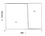
図2に、本実施例1におけるバリア層104(即ち、急峻界面提供層1041と電極接続面提供層1042)形成時のキャリアガス供給形態を示す。このグラフの縦軸はキャリアガス中に占める水素(H2)ガスの分圧比Rを示している。また、横軸は結晶成長時間であり、時刻t=0が急峻界面提供層1041の結晶成長開始時刻を示し、時刻t=t1が電極接続面提供層1042の結晶成長終了時刻を示している。
更に、詳しくは、以下の結晶成長条件にしたがって、バリア層104を積層した。
FIG. 2 shows a carrier gas supply mode when the barrier layer 104 (that is, the steep interface providing layer 1041 and the electrode connection surface providing layer 1042) is formed in the first embodiment. The vertical axis of this graph indicates the partial pressure ratio R of hydrogen (H 2 ) gas in the carrier gas. The horizontal axis represents the crystal growth time. Time t = 0 represents the crystal growth start time of the steep interface providing layer 1041, and time t = t 1 represents the crystal growth end time of the electrode connection
More specifically, the barrier layer 104 was laminated according to the following crystal growth conditions.
(バリア層104の結晶成長条件)
(1)急峻界面提供層1041
(a)キャリアガス : H2 (R≒1)
(b)結晶成長温度 : 1000〔℃〕
(c)結晶成長気圧 : 1013〔hPa〕(結晶成長炉内の全圧)
(Crystal growth conditions for barrier layer 104)
(1) Steep interface providing layer 1041
(A) Carrier gas: H 2 (R≈1)
(B) Crystal growth temperature: 1000 [° C.]
(C) Crystal growth pressure: 1013 [hPa] (total pressure in crystal growth furnace)
(2)電極接続面提供層1042
(a)キャリアガス : N2 (R≒0)
(b)結晶成長温度 : 1000〔℃〕
(c)結晶成長気圧 : 1013〔hPa〕(結晶成長炉内の全圧)
(2) Electrode connection
(A) Carrier gas: N 2 (R≈0)
(B) Crystal growth temperature: 1000 [° C.]
(C) Crystal growth pressure: 1013 [hPa] (total pressure in crystal growth furnace)
図3は、バリア層104全体の厚さ(:d1+d2)を400Åに固定する時、電極接続面提供層1042の膜厚d2〔Å〕をパラメータとして、電極接続面提供層1042の表面の像(表面モフォロジー)を5種類(d2=0Å〜400Å)、原子間力顕微鏡(Atomic Force Microscope)を使って出力したものである。
図4−Aに、この電極接続面提供層1042の膜厚d2と各表面の粗さとの関係を示す。縦軸は、電極接続面提供層1042の表面の1方向における凹凸波形の平均振幅(Root Mean Square)を、d2=0Åの時の値を基準(:規格化表面粗さ=1)として、即ち、膜厚約400Åの急峻界面提供層1041だけでバリア層104全体を形成した場合を基準として、規格化したものである。
FIG. 3 shows that when the thickness (: d 1 + d 2 ) of the entire barrier layer 104 is fixed to 400 mm, the film thickness d 2 [Å] of the electrode connection
FIG. 4-A shows the relationship between the film thickness d 2 of the electrode connection
また、図4−Bのグラフは、ゲート電極106形成前の電界効果トランジスタ100のシート抵抗の規格化値と、上記の膜厚d2との関係を、図4−Aの場合と同様にd2=0Åの時の値を基準(:規格化シート抵抗=1)として示したものである。
これらの測定結果より、バリア層104全体の膜厚を400Åにする場合、電極接続面提供層1042の膜厚d2の適正範囲は、約100Å〜300Å程度の範囲であり、より望ましくは約150Å〜200Å程度の範囲になると言うことができる。
Further, the graph of FIG. 4-B shows the relationship between the normalized value of the sheet resistance of the
From these measurements, when the barrier layer 104 total thickness to 400 Å, a proper range of the thickness d 2 of the electrode connection
この様に、バリア層104を形成した結果、本実施例1の電界効果トランジスタ100においては、シート抵抗などの各種の電気特性を良好に確保でき、同時に良好な表面平坦性に基づいて電極を従来よりも効果的に微細化することができた。
As described above, as a result of forming the barrier layer 104, in the
図5は、本実施例2の電界効果トランジスタ200の断面図である。この電界効果トランジスタ200は、結晶成長によってIII族窒化物系化合物半導体を順次積層することにより形成した半導体素子であり、その結晶成長基板201は、厚さ約400μmの炭化シリコン(SiC)から形成されている。この結晶成長基板201の上には、厚さ約0.2μmのAlNから成るAlN層202が形成されている。このAlN層202は結晶成長基板201と、後に積層する半導体層203との間の格子定数の不整合を解消又は緩和するためのものである。
FIG. 5 is a cross-sectional view of the
そして、このAlN層202の上には厚さ約2μmのノンドープのGaNから成る半導体層203が形成されている。以下、この半導体層203と上記のAlN層202との計2層を合わせて総称的に単にバッファ層と言うことがある。勿論、このバッファ層(層202と層203)が、請求項1などに記載されているバッファ層に相当する半導体層である。
A
更に、半導体層203の上には、厚さ約40nmのノンドープのAl0.25Ga0.75Nから成る半導体層204が積層されている。この半導体層204の膜厚(約40nm)は、ゲートON時にバリア層とバッファ層との界面、即ち、層2041と層203との界面の近傍に生成されるチャネルと、下記の個々のオーミック電極(205,207)との間におけるキャリア(電子)のトンネル効果が、それぞれ確実かつ良好に発現する様に設定されている。
Further, a
即ち、半導体層204は、本発明に基づく厚さ約10nmの急峻界面提供層2041と、本発明に基づく厚さ約30nmの電極接続面提供層2042の計2層の半導体層から構成されている。これらは双方共に上記の通りノンドープのAl0.25Ga0.75Nから形成されているが、急峻界面提供層2041を結晶成長させる際には、キャリアガスとしてH2を使用した。また、電極接続面提供層2042を結晶成長させる際には、キャリアガスとしてN2を使用した。
That is, the
また、符号205,206,207はそれぞれ、ソース電極(オーミック電極)、ゲート電極(ショットキー電極)、ドレイン電極(オーミック電極)を示している。各オーミック電極(ソース電極205とドレイン電極207)は、何れもチタン(Ti)から成る膜厚約100Åの薄い金属層を蒸着によって積層し、その上にアルミニウム(Al)から成る膜厚約3000Åの金属層を更に蒸着にて積層したものである。これらのオーミック電極は、1秒未満のフラッシュアニール処理による約700℃〜900℃の熱処理によって、良好に密着及び合金化されている。他方、ゲート電極206は、約100Åのニッケル(Ni)から成る金属層を蒸着によって積層し、その上に、金(Au)から成る金属層を更に約3000Å蒸着して形成したショットキー電極である。
以下、上記の電界効果トランジスタ200の製造方法を、本発明の特徴部分(半導体層2041,2042)を中心に説明する。
上記の電界効果トランジスタ200の各半導体層(半導体層202,203,204)は何れも、有機金属化合物気相成長法(MOVPE)による気相成長により結晶成長されたものである。ここで用いられたガスは、キャリアガス(H2又はN2)と、アンモニアガス(NH3)と、トリメチルガリウム(Ga(CH3)3)と、トリメチルアルミニウム(Al(CH3)3)などである。
ただし、これらの半導体層を結晶成長させる方法としては、上記の有機金属化合物気相成長法(MOVPE)の他にも、分子線気相成長法(MBE)、ハライド気相成長法(HVPE)等が有効である。
Hereinafter, the manufacturing method of the above-described
Each of the semiconductor layers (semiconductor layers 202, 203, and 204) of the above-described
However, as a method for crystal growth of these semiconductor layers, in addition to the above-mentioned organometallic compound vapor phase epitaxy (MOVPE), molecular beam vapor phase epitaxy (MBE), halide vapor phase epitaxy (HVPE), etc. Is effective.
本実施例2におけるバリア層204(即ち、急峻界面提供層2041と電極接続面提供層2042)形成時のキャリアガス供給形態を、前述の実施例1と同様、図2に示す。このグラフの縦軸は、前述の実施例1と同様、キャリアガス中に占める水素(H2)ガスの分圧比Rを示している。また、横軸は結晶成長時間であり、時刻t=0が急峻界面提供層2041の結晶成長開始時刻を示し、時刻t=t1が電極接続面提供層2042の結晶成長終了時刻を示している。
更に、詳しくは、以下の結晶成長条件にしたがって、バリア層204を積層した。
The carrier gas supply mode at the time of forming the barrier layer 204 (that is, the steep
More specifically, the
(バリア層204の結晶成長条件)
(1)急峻界面提供層2041
(a)キャリアガス : H2 (R≒1)
(b)結晶成長温度 : 1000〔℃〕
(c)結晶成長気圧 : 1013〔hPa〕(結晶成長炉内の全圧)
(Crystal growth conditions for the barrier layer 204)
(1) Steep
(A) Carrier gas: H 2 (R≈1)
(B) Crystal growth temperature: 1000 [° C.]
(C) Crystal growth pressure: 1013 [hPa] (total pressure in crystal growth furnace)
(2)電極接続面提供層2042
(a)キャリアガス : N2 (R≒0)
(b)結晶成長温度 : 1000〔℃〕
(c)結晶成長気圧 : 1013〔hPa〕(結晶成長炉内の全圧)
(2) Electrode connection
(A) Carrier gas: N 2 (R≈0)
(B) Crystal growth temperature: 1000 [° C.]
(C) Crystal growth pressure: 1013 [hPa] (total pressure in crystal growth furnace)
図6は、バリア層204全体の厚さ(:d1+d2)を40nmに固定する時、電極接続面提供層2042の膜厚d2〔Å〕をパラメータとして、電極接続面提供層2042の表面の像を2種類(d2=0nm,30nm)、原子間力顕微鏡(Atomic Force Microscope)を使って出力したものである。
図7−Aに、この電極接続面提供層2042の膜厚d2と各表面の粗さとの関係を示す。縦軸は、電極接続面提供層2042の表面の1方向における凹凸波形の平均振幅(Root Mean Square)を、d2=0Åの時の値を基準(:規格化表面粗さ=1)として、即ち、膜厚約40nmの急峻界面提供層2041だけでバリア層204全体を形成した場合を基準として、規格化したものである。
FIG. 6 shows that when the thickness (: d 1 + d 2 ) of the
FIG. 7A shows the relationship between the film thickness d 2 of the electrode connection
また、図7−Bのグラフは、ゲート電極206形成前の電界効果トランジスタ200のシート抵抗の規格化値と、上記の膜厚d2との関係を、図7−Aの場合と同様にd2=0nmの時の値を基準(:規格化シート抵抗=1)として示したものである。
これらの測定結果からも、所望の電気特性と電極の微細化とを高度かつ合理的に両立させるためには、バリア層204は、急峻界面提供層2041と電極接続面提供層2042との2層構成にすると良いことが判る。
7B shows the relationship between the normalized value of the sheet resistance of the
Also from these measurement results, the
この様に、バリア層204を形成した結果、本実施例2の電界効果トランジスタ200においては、シート抵抗などの各種の電気特性を良好に確保でき、同時に良好な表面平坦性に基づいて電極を従来よりも効果的に微細化することができた。
As described above, as a result of the formation of the
〔その他の変形例〕
本発明の実施形態は、上記の形態に限定されるものではなく、その他にも以下に例示される様な変形を行っても良い。この様な変形や応用によっても、本発明の作用に基づいて本発明の効果を得ることができる。
[Other variations]
The embodiment of the present invention is not limited to the above-described embodiment, and other modifications as exemplified below may be made. Even with such modifications and applications, the effects of the present invention can be obtained based on the functions of the present invention.
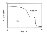
(変形例1)
例えば、上記の実施例1では、図2からも判る様に、キャリアガス中に占める水素ガスの分圧比Rを一度で、略1から略0に一気に減少させたが、その他にも例えば図8に例示する様に、キャリアガス中に占める水素ガスの分圧比Rは、略一様に連続的に減少させる様にしても良い。この様にした場合、上記の様に問題のバリア層104を明確に2層(即ち、急峻界面提供層1041と電極接続面提供層1042)に分けて認識することはできないが、しかしながら、上記の電界効果トランジスタ100と略同等の性能を有する電界効果トランジスタを製造することができる。
(Modification 1)
For example, in the first embodiment, as can be seen from FIG. 2, the partial pressure ratio R of the hydrogen gas occupying the carrier gas is reduced from about 1 to about 0 at a stroke. As illustrated in FIG. 4, the partial pressure ratio R of the hydrogen gas in the carrier gas may be continuously reduced substantially uniformly. In this case, the barrier layer 104 in question cannot be clearly divided into two layers (that is, the steep interface providing layer 1041 and the electrode connection surface providing layer 1042) as described above. A field effect transistor having substantially the same performance as the
(変形例2)
また、キャリアガス中に占める水素ガスの分圧比Rは、多段階に分けて時々刻々と段階的に減少させる様にしても良い。また、なだらかに連続的に減少させたり、急峻に段階的に減少させたりする形態を組み合わせて実施しても良い。図9に例示される実施形態は、その様な組み合わせの形態を例示するものである。
これらの何れの実施形態においても、本発明の手段に基づいて、本発明の作用・効果を得ることができる。
(Modification 2)
Further, the partial pressure ratio R of the hydrogen gas occupying in the carrier gas may be reduced step by step in multiple steps. Further, it may be carried out in combination with a mode in which the current is gradually decreased or rapidly decreased in a stepwise manner. The embodiment illustrated in FIG. 9 exemplifies such a combination form.
In any of these embodiments, the actions and effects of the present invention can be obtained based on the means of the present invention.
本発明は、半導体の表面荒れの防止方法に関し、半導体素子の電極の微細化への可能性または容易性を良好に確保するためのものである。また、同時に本発明は、結晶成長によって積層される半導体層間の界面近傍に略平面状に生成されるチャネル中を移動するキャリアの移動度に関し、その移動度を良好に確保するためのものである。
したがって、本発明は、III族窒化物系化合物半導体の結晶成長によって製造可能な電界効果トランジスタ(各種のFETやHEMT等)の設計や製造に大いに有用なものであり、各種の電界効果トランジスタの小型化や高性能化に当たって非常に大きな効果を発揮する。
The present invention relates to a method for preventing surface roughness of a semiconductor, and is intended to satisfactorily ensure the possibility or ease of miniaturization of electrodes of a semiconductor element. At the same time, the present invention relates to the mobility of carriers moving in a channel generated in a substantially planar shape in the vicinity of the interface between semiconductor layers stacked by crystal growth, in order to ensure good mobility. .
Therefore, the present invention is very useful for the design and manufacture of field effect transistors (such as various FETs and HEMTs) that can be manufactured by crystal growth of group III nitride compound semiconductors. It is very effective in improving performance and performance.
100 : 電界効果トランジスタ(実施例1)
101 : 結晶成長基板(サファイア)
102 : AlN層(バッファ層)
103 : GaNから成る半導体層(バッファ層)
104 : AlGaNから成る半導体層(バリア層)
1041: 急峻界面提供層
1042: 電極接続面提供層
105 : ソース電極(オーミック電極)
106 : ゲート電極(ショットキー電極)
107 : ドレイン電極(オーミック電極)
100: Field effect transistor (Example 1)
101: Crystal growth substrate (sapphire)
102: AlN layer (buffer layer)
103: Semiconductor layer (buffer layer) made of GaN
104: Semiconductor layer (barrier layer) made of AlGaN
1041: Steep interface providing layer 1042: Electrode connection surface providing layer 105: Source electrode (ohmic electrode)
106: Gate electrode (Schottky electrode)
107: drain electrode (ohmic electrode)
200 : 電界効果トランジスタ(実施例2)
201 : 結晶成長基板(SiC)
202 : AlN層(バッファ層)
203 : GaNから成る半導体層(バッファ層)
204 : AlGaNから成る半導体層(バリア層)
2041: 急峻界面提供層
2042: 電極接続面提供層
205 : ソース電極(オーミック電極)
206 : ゲート電極(ショットキー電極)
207 : ドレイン電極(オーミック電極)
200: Field effect transistor (Example 2)
201: Crystal growth substrate (SiC)
202: AlN layer (buffer layer)
203: Semiconductor layer (buffer layer) made of GaN
204: Semiconductor layer (barrier layer) made of AlGaN
2041: Steep interface providing layer 2042: Electrode connection surface providing layer 205: Source electrode (ohmic electrode)
206: Gate electrode (Schottky electrode)
207: Drain electrode (ohmic electrode)
Claims (8)
前記バリア層を結晶成長させる結晶成長工程において、前記バリア層の材料ガスを運ぶキャリアガスの中で、水素(H2)ガスが占めるガス分圧比Rを「r1≧R≧r2(1≧r1>1/4,1/2>r2≧0,r1>r2)」なる範囲内で、時間tに対して連続的又は段階的に、単調に減少させることを特徴とする電界効果トランジスタの製造方法。 A method of manufacturing a field effect transistor, comprising a buffer layer made of a group III nitride compound semiconductor and a barrier layer, wherein a channel is formed on an interface side of the buffer layer with respect to the barrier layer,
In the crystal growth step for crystal growth of the barrier layer, the gas partial pressure ratio R occupied by hydrogen (H 2 ) gas in the carrier gas carrying the material gas of the barrier layer is set to “r 1 ≧ R ≧ r 2 (1 ≧ r 1 > 1/4, 1/2> r 2 ≧ 0, r 1 > r 2 ) ”, and continuously or stepwise with respect to time t. Effect transistor manufacturing method.
先に積層するバリア層第1層を、水素(H2)ガスを主なキャリアガスとして結晶成長させ、
次に積層するバリア層第2層を、希ガス又は窒素(N2)ガスから成る不活性ガスを主なキャリアガスとして結晶成長させることを特徴とする請求項2に記載の電界効果トランジスタの製造方法。 The barrier layer has a two-layer structure,
The barrier layer first layer to be laminated first is crystal-grown using hydrogen (H 2 ) gas as the main carrier gas,
3. The field effect transistor according to claim 2 , wherein the second barrier layer to be laminated is crystal-grown using an inert gas composed of a rare gas or nitrogen (N 2 ) gas as a main carrier gas. Method.
Priority Applications (5)
| Application Number | Priority Date | Filing Date | Title |
|---|---|---|---|
| JP2004176676A JP4729872B2 (en) | 2004-06-15 | 2004-06-15 | Method for manufacturing field effect transistor |
| DE112005001337T DE112005001337B4 (en) | 2004-06-10 | 2005-06-09 | Process for producing a FET |
| US11/578,965 US7981744B2 (en) | 2004-06-10 | 2005-06-09 | Field-effect transistor, semiconductor device, a method for manufacturing them, and a method of semiconductor crystal growth |
| PCT/JP2005/011006 WO2005122234A1 (en) | 2004-06-10 | 2005-06-09 | Field-effect transistor, semiconductor device, a method for manufacturing them, and a method of semiconductor crystal growth |
| TW094119288A TWI299196B (en) | 2004-06-10 | 2005-06-10 | Field-effect transistor, semiconductor device, a method for manufacturing them, and a method of semiconductor crystal growth |
Applications Claiming Priority (1)
| Application Number | Priority Date | Filing Date | Title |
|---|---|---|---|
| JP2004176676A JP4729872B2 (en) | 2004-06-15 | 2004-06-15 | Method for manufacturing field effect transistor |
Publications (3)
| Publication Number | Publication Date |
|---|---|
| JP2006004977A JP2006004977A (en) | 2006-01-05 |
| JP2006004977A5 JP2006004977A5 (en) | 2008-04-17 |
| JP4729872B2 true JP4729872B2 (en) | 2011-07-20 |
Family
ID=35773129
Family Applications (1)
| Application Number | Title | Priority Date | Filing Date |
|---|---|---|---|
| JP2004176676A Expired - Fee Related JP4729872B2 (en) | 2004-06-10 | 2004-06-15 | Method for manufacturing field effect transistor |
Country Status (1)
| Country | Link |
|---|---|
| JP (1) | JP4729872B2 (en) |
Families Citing this family (4)
| Publication number | Priority date | Publication date | Assignee | Title |
|---|---|---|---|---|
| JP2007220927A (en) * | 2006-02-17 | 2007-08-30 | Tokyo Univ Of Agriculture & Technology | Manufacturing method of algan ternary mixed crystal, and vapor phase epitaxy apparatus |
| JP5217151B2 (en) * | 2006-08-25 | 2013-06-19 | 日亜化学工業株式会社 | Field effect transistor and manufacturing method thereof |
| JP5230560B2 (en) * | 2009-08-07 | 2013-07-10 | コバレントマテリアル株式会社 | Compound semiconductor substrate and manufacturing method thereof |
| JP5286616B2 (en) * | 2011-07-22 | 2013-09-11 | 国立大学法人東京農工大学 | Method for producing AlxGa1-xN crystal |
Citations (2)
| Publication number | Priority date | Publication date | Assignee | Title |
|---|---|---|---|---|
| WO2003049193A1 (en) * | 2001-12-03 | 2003-06-12 | Cree, Inc. | Strain balanced nitride heterojunction transistors and methods of fabricating strain balanced nitride heterojunction transistors |
| JP2005509274A (en) * | 2001-05-11 | 2005-04-07 | クリー インコーポレイテッド | III-nitride high electron mobility transistor (HEMT) with barrier / spacer layer |
Family Cites Families (1)
| Publication number | Priority date | Publication date | Assignee | Title |
|---|---|---|---|---|
| JPH11261051A (en) * | 1998-03-09 | 1999-09-24 | Nippon Telegr & Teleph Corp <Ntt> | Semiconductor device |
-
2004
- 2004-06-15 JP JP2004176676A patent/JP4729872B2/en not_active Expired - Fee Related
Patent Citations (2)
| Publication number | Priority date | Publication date | Assignee | Title |
|---|---|---|---|---|
| JP2005509274A (en) * | 2001-05-11 | 2005-04-07 | クリー インコーポレイテッド | III-nitride high electron mobility transistor (HEMT) with barrier / spacer layer |
| WO2003049193A1 (en) * | 2001-12-03 | 2003-06-12 | Cree, Inc. | Strain balanced nitride heterojunction transistors and methods of fabricating strain balanced nitride heterojunction transistors |
Also Published As
| Publication number | Publication date |
|---|---|
| JP2006004977A (en) | 2006-01-05 |
Similar Documents
| Publication | Publication Date | Title |
|---|---|---|
| JP4525894B2 (en) | Semiconductor device forming plate-like substrate, manufacturing method thereof, and semiconductor device using the same | |
| US9818855B2 (en) | Semiconductor device | |
| JP4381380B2 (en) | Semiconductor device and manufacturing method thereof | |
| JP4530171B2 (en) | Semiconductor device | |
| JP5634681B2 (en) | Semiconductor element | |
| JP5116977B2 (en) | Semiconductor element | |
| JP5749580B2 (en) | Semiconductor device and manufacturing method of semiconductor device | |
| US8592823B2 (en) | Compound semiconductor device and method for manufacturing the same | |
| JP2003059948A (en) | Semiconductor device and production method therefor | |
| JP2010171416A (en) | Semiconductor device, manufacturing method therefor, and leakage-current reduction method therefor | |
| US20220376074A1 (en) | Nitride-based semiconductor device and method for manufacturing the same | |
| WO2005122234A1 (en) | Field-effect transistor, semiconductor device, a method for manufacturing them, and a method of semiconductor crystal growth | |
| US9379102B2 (en) | Nitride-based semiconductor device | |
| JP4888537B2 (en) | Group III nitride semiconductor laminated wafer and group III nitride semiconductor device | |
| CN111344868B (en) | High electron mobility transistor with boron nitride alloy interlayer and method of manufacture | |
| US7432538B2 (en) | Field-effect transistor | |
| JP5101143B2 (en) | Field effect transistor and manufacturing method thereof | |
| JP2007088252A5 (en) | ||
| JP2007123824A (en) | Electronic device using group-iii nitride based compound semiconductor | |
| JP4729872B2 (en) | Method for manufacturing field effect transistor | |
| JP5223202B2 (en) | Semiconductor substrate and semiconductor device | |
| JP4682541B2 (en) | Semiconductor crystal growth method | |
| JP2006004977A5 (en) | ||
| JP6168978B2 (en) | Nitride semiconductor device, method for manufacturing the same, diode, and field effect transistor | |
| CN110875381B (en) | Semiconductor device and manufacturing method thereof |
Legal Events
| Date | Code | Title | Description |
|---|---|---|---|
| A621 | Written request for application examination |
Free format text: JAPANESE INTERMEDIATE CODE: A621 Effective date: 20060830 |
|
| A521 | Written amendment |
Free format text: JAPANESE INTERMEDIATE CODE: A523 Effective date: 20080304 |
|
| A131 | Notification of reasons for refusal |
Free format text: JAPANESE INTERMEDIATE CODE: A131 Effective date: 20100824 |
|
| A521 | Written amendment |
Free format text: JAPANESE INTERMEDIATE CODE: A523 Effective date: 20101021 |
|
| A01 | Written decision to grant a patent or to grant a registration (utility model) |
Free format text: JAPANESE INTERMEDIATE CODE: A01 Effective date: 20110322 |
|
| A61 | First payment of annual fees (during grant procedure) |
Free format text: JAPANESE INTERMEDIATE CODE: A61 Effective date: 20110404 |
|
| FPAY | Renewal fee payment (event date is renewal date of database) |
Free format text: PAYMENT UNTIL: 20140428 Year of fee payment: 3 |
|
| R150 | Certificate of patent or registration of utility model |
Free format text: JAPANESE INTERMEDIATE CODE: R150 |
|
| LAPS | Cancellation because of no payment of annual fees |