EP2562584A2 - Anzeige und elektronische Einheit - Google Patents
Anzeige und elektronische Einheit Download PDFInfo
- Publication number
- EP2562584A2 EP2562584A2 EP12177325A EP12177325A EP2562584A2 EP 2562584 A2 EP2562584 A2 EP 2562584A2 EP 12177325 A EP12177325 A EP 12177325A EP 12177325 A EP12177325 A EP 12177325A EP 2562584 A2 EP2562584 A2 EP 2562584A2
- Authority
- EP
- European Patent Office
- Prior art keywords
- display
- substrate
- layer
- damp
- driving
- Prior art date
- Legal status (The legal status is an assumption and is not a legal conclusion. Google has not performed a legal analysis and makes no representation as to the accuracy of the status listed.)
- Withdrawn
Links
Images




Classifications
-
- G—PHYSICS
- G09—EDUCATION; CRYPTOGRAPHY; DISPLAY; ADVERTISING; SEALS
- G09F—DISPLAYING; ADVERTISING; SIGNS; LABELS OR NAME-PLATES; SEALS
- G09F9/00—Indicating arrangements for variable information in which the information is built-up on a support by selection or combination of individual elements
- G09F9/30—Indicating arrangements for variable information in which the information is built-up on a support by selection or combination of individual elements in which the desired character or characters are formed by combining individual elements
- G09F9/35—Indicating arrangements for variable information in which the information is built-up on a support by selection or combination of individual elements in which the desired character or characters are formed by combining individual elements being liquid crystals
-
- G—PHYSICS
- G02—OPTICS
- G02F—OPTICAL DEVICES OR ARRANGEMENTS FOR THE CONTROL OF LIGHT BY MODIFICATION OF THE OPTICAL PROPERTIES OF THE MEDIA OF THE ELEMENTS INVOLVED THEREIN; NON-LINEAR OPTICS; FREQUENCY-CHANGING OF LIGHT; OPTICAL LOGIC ELEMENTS; OPTICAL ANALOGUE/DIGITAL CONVERTERS
- G02F1/00—Devices or arrangements for the control of the intensity, colour, phase, polarisation or direction of light arriving from an independent light source, e.g. switching, gating or modulating; Non-linear optics
- G02F1/01—Devices or arrangements for the control of the intensity, colour, phase, polarisation or direction of light arriving from an independent light source, e.g. switching, gating or modulating; Non-linear optics for the control of the intensity, phase, polarisation or colour
- G02F1/13—Devices or arrangements for the control of the intensity, colour, phase, polarisation or direction of light arriving from an independent light source, e.g. switching, gating or modulating; Non-linear optics for the control of the intensity, phase, polarisation or colour based on liquid crystals, e.g. single liquid crystal display cells
- G02F1/133—Constructional arrangements; Operation of liquid crystal cells; Circuit arrangements
- G02F1/1333—Constructional arrangements; Manufacturing methods
-
- G—PHYSICS
- G02—OPTICS
- G02F—OPTICAL DEVICES OR ARRANGEMENTS FOR THE CONTROL OF LIGHT BY MODIFICATION OF THE OPTICAL PROPERTIES OF THE MEDIA OF THE ELEMENTS INVOLVED THEREIN; NON-LINEAR OPTICS; FREQUENCY-CHANGING OF LIGHT; OPTICAL LOGIC ELEMENTS; OPTICAL ANALOGUE/DIGITAL CONVERTERS
- G02F1/00—Devices or arrangements for the control of the intensity, colour, phase, polarisation or direction of light arriving from an independent light source, e.g. switching, gating or modulating; Non-linear optics
- G02F1/01—Devices or arrangements for the control of the intensity, colour, phase, polarisation or direction of light arriving from an independent light source, e.g. switching, gating or modulating; Non-linear optics for the control of the intensity, phase, polarisation or colour
- G02F1/13—Devices or arrangements for the control of the intensity, colour, phase, polarisation or direction of light arriving from an independent light source, e.g. switching, gating or modulating; Non-linear optics for the control of the intensity, phase, polarisation or colour based on liquid crystals, e.g. single liquid crystal display cells
- G02F1/133—Constructional arrangements; Operation of liquid crystal cells; Circuit arrangements
- G02F1/1333—Constructional arrangements; Manufacturing methods
- G02F1/133305—Flexible substrates, e.g. plastics, organic film
-
- G—PHYSICS
- G02—OPTICS
- G02F—OPTICAL DEVICES OR ARRANGEMENTS FOR THE CONTROL OF LIGHT BY MODIFICATION OF THE OPTICAL PROPERTIES OF THE MEDIA OF THE ELEMENTS INVOLVED THEREIN; NON-LINEAR OPTICS; FREQUENCY-CHANGING OF LIGHT; OPTICAL LOGIC ELEMENTS; OPTICAL ANALOGUE/DIGITAL CONVERTERS
- G02F1/00—Devices or arrangements for the control of the intensity, colour, phase, polarisation or direction of light arriving from an independent light source, e.g. switching, gating or modulating; Non-linear optics
- G02F1/01—Devices or arrangements for the control of the intensity, colour, phase, polarisation or direction of light arriving from an independent light source, e.g. switching, gating or modulating; Non-linear optics for the control of the intensity, phase, polarisation or colour
- G02F1/13—Devices or arrangements for the control of the intensity, colour, phase, polarisation or direction of light arriving from an independent light source, e.g. switching, gating or modulating; Non-linear optics for the control of the intensity, phase, polarisation or colour based on liquid crystals, e.g. single liquid crystal display cells
- G02F1/133—Constructional arrangements; Operation of liquid crystal cells; Circuit arrangements
- G02F1/1333—Constructional arrangements; Manufacturing methods
- G02F1/133308—Support structures for LCD panels, e.g. frames or bezels
- G02F1/133311—Environmental protection, e.g. against dust or humidity
-
- G—PHYSICS
- G02—OPTICS
- G02F—OPTICAL DEVICES OR ARRANGEMENTS FOR THE CONTROL OF LIGHT BY MODIFICATION OF THE OPTICAL PROPERTIES OF THE MEDIA OF THE ELEMENTS INVOLVED THEREIN; NON-LINEAR OPTICS; FREQUENCY-CHANGING OF LIGHT; OPTICAL LOGIC ELEMENTS; OPTICAL ANALOGUE/DIGITAL CONVERTERS
- G02F2201/00—Constructional arrangements not provided for in groups G02F1/00 - G02F7/00
- G02F2201/50—Protective arrangements
- G02F2201/501—Blocking layers, e.g. against migration of ions
-
- G—PHYSICS
- G02—OPTICS
- G02F—OPTICAL DEVICES OR ARRANGEMENTS FOR THE CONTROL OF LIGHT BY MODIFICATION OF THE OPTICAL PROPERTIES OF THE MEDIA OF THE ELEMENTS INVOLVED THEREIN; NON-LINEAR OPTICS; FREQUENCY-CHANGING OF LIGHT; OPTICAL LOGIC ELEMENTS; OPTICAL ANALOGUE/DIGITAL CONVERTERS
- G02F2202/00—Materials and properties
- G02F2202/28—Adhesive materials or arrangements
Definitions
- the present technology relates to a display including a liquid crystal layer, and an electronic unit including the display.
- liquid crystal displays As displays for reading, displays of cholesteric liquid crystal type, electrophoresis type, electric oxidation reduction type, and twist ball type are proposed. Above all, liquid crystal displays that generate contrast by utilizing variation in orientation of liquid crystal molecules are preferable. In particular, in consideration of handleability or the like, liquid crystal displays of flexible type using a flexible plastic film or the like as a supporting base are more preferable.
- displays classified as reflection type are also preferable.
- the reason for this is that since such displays utilize reflection (scattering) of external light similarly to a paper in order to perform bright display, display quality close to that of the paper is obtained, and that since a backlight is unnecessary, power consumption is reduced.
- a leading candidate of the displays of the reflection type is electrophoretic displays that utilize the electrophoresis of electric charge particles to generate contrast. This is because electrophoretic displays offer low power consumption and very quick response.
- the electrophoretic display is provided with a display substrate including an electrophoretic element, and a driving substrate including a thin film transistor (TFT) that drives the display substrate and the like.
- TFT thin film transistor
- a display substrate is covered with a protective layer in order to prevent a situation in which the movement of electric charge particles is interfered by intrusion of water.
- a protective layer is provided on a top face of a display substrate, and a sealing material is formed on side faces of the display substrate (see, for example, Japanese Unexamined Patent Application Publication No. 2009-134324 ).
- a display substrate is covered by a protective layer, and end portions of the protective layer are adhered to a surface of a driving substrate through an adhesive agent (see, for example, Published Japanese Translation of PCT Application No. JP 2009-529711 ).
- a display including: a display substrate including a liquid crystal layer; a driving substrate driving the display substrate; and a damp-proof layer continuously provided along a top face and side faces of the display substrate, and a top face of the driving substrate.
- an electronic unit including a display, the display including: a display substrate including a liquid crystal layer; a driving substrate driving the display substrate; and a damp-proof layer continuously provided along a top face and side faces of the display substrate, and a top face of the driving substrate.
- FIG. 1 is a sectional view showing a configuration of a display according to an embodiment of the present technology.
- FIG. 2 is a sectional view showing a modification with respect to the configuration of the display.
- FIGs. 3A and 3B are perspective views each showing a configuration of an electronic book provided with the display.
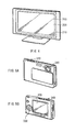
- FIG. 4 is a perspective view showing a configuration of a television provided with the display.
- FIGs. 5A and 5B are perspective views each showing a configuration of a digital still camera provided with the display.
- FIG. 6 is a perspective view showing an external appearance of a personal computer provided with the display.
- FIG. 7 is a perspective view showing an external appearance of a video camera provided with the display.
- FIGs. 8A to 8G are plan views each showing a configuration of a mobile phone provided with the display.
- FIG. 1 shows a cross-sectional configuration of the display.
- This display is applicable to various kinds of electronic units, and the kind of electronic unit is not particularly limited.
- the display described here is a liquid crystal display device (so-called liquid crystal display) which utilizes variation in orientation of liquid crystal molecules to display an image.
- a driving substrate 10 and a display substrate 20 are disposed to face each other with a spacer 30 and a liquid crystal layer 31 therebetween as illustrated in FIG. 1 , and an image is displayed on the display substrate 20 side.
- the driving substrate 10 and the display substrate 20 are provided with a damp-proof layer 42.
- the driving substrate 10 includes a thin film transistor (TFT) 12, a protective layer 13, a planarizing insulating layer 14, a pixel electrode 15 which are formed on the entire surface of a supporting base 11 in this order, for example.
- TFT 12 and the pixel electrode 15 are disposed in matrix or a segmented form corresponding to a pixel placement, for example.
- the supporting base 11 is, for example, made of one or more kinds of inorganic materials, metal materials, plastic materials, and the like.
- the inorganic materials include silicon (Si), silicon oxide (SiO x ), silicon nitride (SiN x ), aluminum oxide (AlO x ), and the like, and the silicon oxide includes glass, spin on glass (SOG), and the like, for example.
- the metal materials include aluminum (Al), nickel (Ni), stainless, and the like.
- the plastic materials include polycarbonate (PC), polyethylene terephthalate (PET), polyethylene naphthalate (PEN), polyether ether ketone (PEEK), and the like.
- the supporting base 11 may be of light transmission type or non-light transmission type. Since an image is displayed on the display substrate 20 side, the supporting base 11 is not necessarily of the light transmission type.
- the supporting base 11 may be configured of either a substrate having rigidity such as a wafer, or a thin layer glass or a film having flexibility, the supporting base 11 preferably has flexibility. This is because, in this case, a flexible (bendable) liquid crystal display is realized.
- the TFT 12 is a switching device configured to select pixels.
- the TFT 12 may be configured of an inorganic TFT employing as a channel layer an inorganic semiconductor layer of amorphous silicon, poly silicon, or oxide, or an organic TFT employing as a channel layer an organic semiconductor layer of pentacene or the like, for example.
- the protective layer 13 and the planarizing insulating layer 14 each contains, for example, an insulating material such as polyimide. It is to be noted that, in the case where the surface of the protective layer 13 is sufficiently flat, the planarizing insulating layer 14 is not necessary.
- the pixel electrode 15 includes one or more kinds of conductive materials such as gold (Au), silver (Ag), and copper (Cu), for example.
- the pixel electrode 15 is connected to the TFT 12 through a contact hole (not shown) provided in the protective layer 13 and the planarizing insulating layer 14. It should be noted that, the number of the TFT 12 disposed for each pixel electrode 15 is not particularly limited, and the number may be one or two or more.
- the display substrate 20 is a substrate in which an opposite electrode 22 is formed on the entire surface of a supporting substrate 21, for example.
- the supporting substrate 21 is made of a material similar to that of the supporting base 11 except that the supporting substrate 21 is of a light transmission type. Since an image is displayed on the display substrate 20 side, it is necessary for the supporting substrate 21 to have light permeability. In particular, similarly to the above-mentioned supporting base 11, in order to realize a flexible type liquid crystal display, the supporting substrate 21 preferably has flexibility.
- the opposite electrode 22 includes, for example, one or more kinds of light-transmissive conductive materials (transparent electrode materials).
- the light-transmissive conductive materials include indium tin oxide (ITO), antimony tin oxide (ATO), fluorine doped tin oxide (FTO), aluminum doped zinc oxide (AZO), and the like.
- the opposite electrode 22 is formed on the entire surface of the supporting substrate 21, for example. It is to be noted that, the opposite electrode 22 is disposed in matrix or a segmented form, similarly to the pixel electrode 15.
- the light transmittance of the opposite electrode 22 is set as high as possible, and for example, the light transmittance is set to 80% or more.
- the electric resistance of the opposite electrode 22 is set to 100 ⁇ / ⁇ or lower.
- the spacer 30 is configured to keep the distance between the driving substrate 10 and the display substrate 20 constant, and the material and form thereof is not particularly limited.
- the liquid crystal layer 31 contains a plurality of liquid crystal molecules, and utilizes variations in orientation of the liquid crystal molecules to generate contrast.
- the orientational state of the liquid crystal molecules is variable in response to electric field, and the kind of the liquid crystal molecules (liquid crystal material) is not particularly limited.
- the damp-proof layer 42 is continuously provided along a top face 20T and side faces 20S of the display substrate 20 and a top face 10T of the driving substrate 10. More specifically, for example, the damp-proof layer 42 is adhered to the display substrate 20 and the driving substrate 10 through an adhesive layer 41 continuously provided along, in this order, the top face 10T, the side face 20S, the top face 20T, the side face 20S, and the top face 10T. With this configuration, the driving substrate 10 and the display substrate 20 is covered with the damp-proof layer 42 which is a single continuous layer, and the damp-proof layer 42 is tightly adhered to the driving substrate 10 and the display substrate 20. Therefore, there is substantially no gap between the damp-proof layer 42 and the driving substrate 10, and between the damp-proof layer 42 and the display substrate 20.
- the adhesive layer 41 includes, for example, one or more kinds of pressure-sensitive adhesive agents and heat-sensitive adhesive agents.
- the damp-proof layer 42 is a so-called water vapor barrier film, and includes one or more kinds of inorganic materials, polymer materials, and the like, for example.
- the inorganic materials include silicon nitride (SiN), silicon oxide (SiO x ), and aluminum oxide (Al 2 O x ).
- the polymer materials include polyethylene terephthalate, polymethylmethacrylate, polycarbonate, polyethylene naphthalate, polypropylene, nylon-6, nylon-66, poly vinylidene chloride, polyether sulfone, and the like.
- the damp-proof property (moisture permeability or water transmittance) of the damp-proof layer 42 is preferably, for example, 0. 1 g/m 2 per day to 0. 000001 g/m 2 per day, more preferably, 0. 03 g/m 2 per day or lower. The reason for this is that since intrusion of water is sufficiently prevented, the display performance of the display is less likely to be lowered. In addition, it is preferable to set the light transmittance of the damp-proof layer 42 as high as possible.
- the liquid crystal display may include other configuration elements such as a retardation plate, a polarization plate, an alighnment film, a backlight unit, and the like (which are not shown), for example.
- the orientational state of liquid crystal molecules in the liquid crystal layer 31 is varied in response to the intensity of the electric field. Consequently, the transmission amount (transmittance) of light is controlled according to the orientational state of the liquid crystal molecules, and thus an image is displayed.
- the display is manufactured by the following procedure.
- the TFT 12, the protective layer 13, the planarizing insulating layer 14, and the pixel electrode 15 are formed in this order on the entire surface of the supporting base 11 to prepare the driving substrate 10.
- the opposite electrode 22 is formed on the entire surface of the supporting substrate 21 to form the display substrate 20.
- the method of forming the composing elements may be appropriately selected from among existing film formation methods, patterning methods, and the like, for example.
- liquid crystal is injected into a space surrounded by the substrates and the spacer 30 to form the liquid crystal layer 31.
- the damp-proof layer 42 is adhered to the driving substrate 10 and the display substrate 20 with the adhesive layer 41 in between. In this way, the display is completed.
- the damp-proof layer 42 is continuously provided along the top face 10T of the driving substrate 10 and the top face 20T and the side faces 20S of the display substrate 20.
- the damp-proof layer 42 is a single continuous layer, and different from a known case where the damp-proof layer 42 is composed of separately formed two components (for example, the known protective layer and sealing material)
- the damp-proof layer 42 of the present embodiment has no joint line. This suppresses intrusion of water into the inside from the outside of the display substrate 20 by way of the joint line.
- the damp-proof layer 42 is formed as a single continuous layer, the damp-proof layer 42 may be formed by one process, and therefore, in comparison to the case where two processes are necessitated to form the damp-proof layer 42 composed of two components, the damp-proof layer 42 is allowed to be readily formed.
- the damp-proof layer 42 is adhered to the driving substrate 10 and the display substrate 20 with the adhesive layer 41 in between, the adhesive layer 41 provided along the top face 20T, the side faces 20S, and the top face 10T, a gap is unlikely to be formed between the damp-proof layer 42 and the side faces 20S.
- the adhesive layer 41 is not provided on the side faces 20S, intrusion of water is prevented at the side faces 20S not only by the damp-proof layer 42 but also by the adhesive layer 41. Consequently, the higher effects are obtainable.
- the function layer 52 is, for example, an anti reflection (AR) film, an anti glare (AG) film, or the like. It is to be noted that, the function layer 52 may also be a layer having other functions, and may also be a layer in which two or more kinds of layers having different functions are laminated. At the time of forming the function layer 52, for example, the function layer 52 may be adhered to the damp-proof layer 42 through the adhesive layer 51 with use of a laminating machine or the like.
- AR anti reflection
- AG anti glare
- the function layer 52 is previously adhered to the damp-proof layer 42 with the adhesive layer 51 in between, and the damp-proof layer 42, together with the function layer 52, is adhered to the driving substrate 10 and the display substrate 20.
- the function layer 52 is adopted, various functions may be added to the display.
- FIGs. 3A and 3B each show an external configuration of an electronic book.
- This electronic book includes, for example, a display section 110, a non-display section (housing) 120, and an operation section 130.
- the operation section 130 may be provided on a front face of the non-display section 120 as illustrated in FIG 3A , or on a top face of the non-display section 120 as illustrated in FIG 3B .
- the display may be incorporated in a PDA having a configuration similar to that of the electronic book illustrated in FIGs. 3A and 3B .
- FIG. 4 shows an external configuration of a television.
- This television is provided with, for example, an image display screen section 200 including a front panel 210 and a filter glass 220.
- FIGs. 5A and 5B each show an external configuration of a digital still camera.
- FIGs. 5A and 5B illustrate a front face and a rear face thereof, respectively.
- This digital still camera includes, for example, a light emitting section 310 for generating flash light, a display section 320, a menu switch 330, and a shutter button 340.
- FIG. 6 shows an external configuration of a notebook personal computer.
- This notebook personal computer includes, for example, a main body 410, a keyboard 420 for inputting letters and the like, and a display section 430 displaying an image.
- FIG. 7 shows an external configuration of a video camera.
- This video camera includes, for example, a main body section 510, a lens 520 which is adapted to take an image of a subject and provided on the front side of the main body section 510, a start/stop switch 530 for capturing an image, and a display section 540.
- FIGs. 8A to 8G each show an external configuration of a mobile phone.
- FIGs. 8A and 8B illustrate a front face and a side face of the mobile phone in an unfolded state, respectively.
- FIGs. 8C to 8G illustrate a front face, a left side face, a right side face, a top face, and a bottom face of the mobile phone in a folded state, respectively.
- This mobile phone includes, for example, an upper side housing 610, a lower side housing 620, a connecting section (hinge section) 630 connecting the upper side housing 610 and the lower side housing 620, a display 640, a sub-display 650, a picture light 660, and a camera 670.
- the present technology has been described based on the embodiment, the present technology is not limited to the modes described in the embodiment, and various modifications may be made.
- the display according to the embodiment of the present technology is applicable to other electronic units in addition to the above-mentioned electronic units.
- “Other electronic units” include, for example, an electrophoretic display and the like.
Landscapes
- Physics & Mathematics (AREA)
- Nonlinear Science (AREA)
- Chemical & Material Sciences (AREA)
- Crystallography & Structural Chemistry (AREA)
- General Physics & Mathematics (AREA)
- Mathematical Physics (AREA)
- Optics & Photonics (AREA)
- Engineering & Computer Science (AREA)
- Theoretical Computer Science (AREA)
- Liquid Crystal (AREA)
- Devices For Indicating Variable Information By Combining Individual Elements (AREA)
Applications Claiming Priority (1)
| Application Number | Priority Date | Filing Date | Title |
|---|---|---|---|
| JP2011181360A JP2013044860A (ja) | 2011-08-23 | 2011-08-23 | 表示装置および電子機器 |
Publications (2)
| Publication Number | Publication Date |
|---|---|
| EP2562584A2 true EP2562584A2 (de) | 2013-02-27 |
| EP2562584A3 EP2562584A3 (de) | 2013-03-27 |
Family
ID=46832201
Family Applications (1)
| Application Number | Title | Priority Date | Filing Date |
|---|---|---|---|
| EP12177325A Withdrawn EP2562584A3 (de) | 2011-08-23 | 2012-07-20 | Anzeige und elektronische Einheit |
Country Status (6)
| Country | Link |
|---|---|
| US (1) | US8829791B2 (de) |
| EP (1) | EP2562584A3 (de) |
| JP (1) | JP2013044860A (de) |
| KR (1) | KR20130023083A (de) |
| CN (1) | CN102955280A (de) |
| TW (1) | TW201310119A (de) |
Families Citing this family (4)
| Publication number | Priority date | Publication date | Assignee | Title |
|---|---|---|---|---|
| KR101977708B1 (ko) * | 2012-09-04 | 2019-08-29 | 삼성디스플레이 주식회사 | 표시 장치 및 그 제조 방법 |
| JP2014202934A (ja) * | 2013-04-05 | 2014-10-27 | ソニー株式会社 | 表示装置および電子機器 |
| CN104698692A (zh) | 2013-12-10 | 2015-06-10 | 精工爱普生株式会社 | 电光装置以及电子设备 |
| KR101676770B1 (ko) * | 2014-10-22 | 2016-11-17 | 삼성디스플레이 주식회사 | 액정 표시 장치 및 그 제조 방법 |
Citations (2)
| Publication number | Priority date | Publication date | Assignee | Title |
|---|---|---|---|---|
| JP2009134324A (ja) | 2002-06-10 | 2009-06-18 | E Ink Corp | 電気光学表示装置を形成および検査するための構成部品および方法 |
| JP2009529711A (ja) | 2006-03-09 | 2009-08-20 | イー インク コーポレイション | エッジシールを有する電気光学表示素子 |
Family Cites Families (9)
| Publication number | Priority date | Publication date | Assignee | Title |
|---|---|---|---|---|
| US6605826B2 (en) * | 2000-08-18 | 2003-08-12 | Semiconductor Energy Laboratory Co., Ltd. | Light-emitting device and display device |
| WO2003003108A1 (en) * | 2001-06-29 | 2003-01-09 | Citizen Watch Co., Ltd. | Liquid crystal display panel and its manufacturing method |
| JP2005123012A (ja) * | 2003-10-16 | 2005-05-12 | Pioneer Electronic Corp | 有機エレクトロルミネセンス表示パネルとその製造方法 |
| US7205718B2 (en) * | 2004-06-24 | 2007-04-17 | Eastman Kodak Company | OLED display having thermally conductive adhesive |
| KR100879207B1 (ko) * | 2005-12-30 | 2009-01-16 | 주식회사 엘지화학 | 플렉시블 디스플레이장치 및 이의 제조방법 |
| TWI421607B (zh) * | 2006-08-24 | 2014-01-01 | Creator Technology Bv | 可撓性裝置上的滲透阻障 |
| CN101154010A (zh) * | 2006-09-29 | 2008-04-02 | 启萌科技有限公司 | 电子纸装置 |
| TWI587734B (zh) * | 2009-03-26 | 2017-06-11 | 精工愛普生股份有限公司 | 有機el裝置、有機el裝置之製造方法、及電子機器 |
| KR101089715B1 (ko) * | 2009-11-05 | 2011-12-07 | 한국기계연구원 | 다층 박막형 봉지막 및 이의 제조방법 |
-
2011
- 2011-08-23 JP JP2011181360A patent/JP2013044860A/ja not_active Abandoned
-
2012
- 2012-07-20 EP EP12177325A patent/EP2562584A3/de not_active Withdrawn
- 2012-07-25 TW TW101126856A patent/TW201310119A/zh unknown
- 2012-08-14 KR KR1020120088758A patent/KR20130023083A/ko not_active Withdrawn
- 2012-08-16 CN CN2012102924005A patent/CN102955280A/zh active Pending
- 2012-08-17 US US13/588,480 patent/US8829791B2/en not_active Expired - Fee Related
Patent Citations (2)
| Publication number | Priority date | Publication date | Assignee | Title |
|---|---|---|---|---|
| JP2009134324A (ja) | 2002-06-10 | 2009-06-18 | E Ink Corp | 電気光学表示装置を形成および検査するための構成部品および方法 |
| JP2009529711A (ja) | 2006-03-09 | 2009-08-20 | イー インク コーポレイション | エッジシールを有する電気光学表示素子 |
Also Published As
| Publication number | Publication date |
|---|---|
| US20130050632A1 (en) | 2013-02-28 |
| TW201310119A (zh) | 2013-03-01 |
| JP2013044860A (ja) | 2013-03-04 |
| KR20130023083A (ko) | 2013-03-07 |
| EP2562584A3 (de) | 2013-03-27 |
| CN102955280A (zh) | 2013-03-06 |
| US8829791B2 (en) | 2014-09-09 |
Similar Documents
| Publication | Publication Date | Title |
|---|---|---|
| JP7542122B2 (ja) | 表示パネル | |
| KR102583494B1 (ko) | 표시 장치 | |
| JP7499924B2 (ja) | El表示装置、電子機器 | |
| JP2023174828A (ja) | 表示装置 | |
| US10073490B2 (en) | Display and electronic unit | |
| US20130120227A1 (en) | Display and electronic unit | |
| JP7478857B2 (ja) | 光経路制御部材及びこれを含むディスプレイ装置 | |
| US9242424B2 (en) | Display device and electronic apparatus | |
| TW201435430A (zh) | 液晶顯示裝置及電子裝置 | |
| US8829791B2 (en) | Display and electronic unit | |
| JP2024050542A (ja) | 発光装置 | |
| US20100302614A1 (en) | Mems and electrophoretic display devices integrated with organic light-emitting device | |
| TWI761320B (zh) | 顯示裝置及電子裝置 | |
| CN113436543B (zh) | 一种显示装置 | |
| CN104103219B (zh) | 显示单元和电子装置 | |
| CN110456579A (zh) | 显示模组及电子设备 | |
| TWI764877B (zh) | 顯示裝置 | |
| CN113724589A (zh) | 显示屏及显示装置 | |
| WO2017199122A1 (ja) | 電子機器 | |
| KR20050094524A (ko) | 광 셔터를 갖는 양방향 디스플레이 장치 | |
| KR20010077355A (ko) | 접이식 평판표시장치 |
Legal Events
| Date | Code | Title | Description |
|---|---|---|---|
| PUAL | Search report despatched |
Free format text: ORIGINAL CODE: 0009013 |
|
| PUAI | Public reference made under article 153(3) epc to a published international application that has entered the european phase |
Free format text: ORIGINAL CODE: 0009012 |
|
| 17P | Request for examination filed |
Effective date: 20120809 |
|
| AK | Designated contracting states |
Kind code of ref document: A2 Designated state(s): AL AT BE BG CH CY CZ DE DK EE ES FI FR GB GR HR HU IE IS IT LI LT LU LV MC MK MT NL NO PL PT RO RS SE SI SK SM TR |
|
| AX | Request for extension of the european patent |
Extension state: BA ME |
|
| AK | Designated contracting states |
Kind code of ref document: A3 Designated state(s): AL AT BE BG CH CY CZ DE DK EE ES FI FR GB GR HR HU IE IS IT LI LT LU LV MC MK MT NL NO PL PT RO RS SE SI SK SM TR |
|
| AX | Request for extension of the european patent |
Extension state: BA ME |
|
| RIC1 | Information provided on ipc code assigned before grant |
Ipc: G02F 1/1333 20060101AFI20130215BHEP |
|
| STAA | Information on the status of an ep patent application or granted ep patent |
Free format text: STATUS: THE APPLICATION HAS BEEN WITHDRAWN |
|
| 18W | Application withdrawn |
Effective date: 20150108 |