EP2562526B1 - Device and method for detecting optical performance of beam shaping element - Google Patents
Device and method for detecting optical performance of beam shaping element Download PDFInfo
- Publication number
- EP2562526B1 EP2562526B1 EP11838977.4A EP11838977A EP2562526B1 EP 2562526 B1 EP2562526 B1 EP 2562526B1 EP 11838977 A EP11838977 A EP 11838977A EP 2562526 B1 EP2562526 B1 EP 2562526B1
- Authority
- EP
- European Patent Office
- Prior art keywords
- far field
- imaging lens
- field imaging
- optical element
- diffractive
- Prior art date
- Legal status (The legal status is an assumption and is not a legal conclusion. Google has not performed a legal analysis and makes no representation as to the accuracy of the status listed.)
- Active
Links
Images
Classifications
-
- B—PERFORMING OPERATIONS; TRANSPORTING
- B23—MACHINE TOOLS; METAL-WORKING NOT OTHERWISE PROVIDED FOR
- B23K—SOLDERING OR UNSOLDERING; WELDING; CLADDING OR PLATING BY SOLDERING OR WELDING; CUTTING BY APPLYING HEAT LOCALLY, e.g. FLAME CUTTING; WORKING BY LASER BEAM
- B23K26/00—Working by laser beam, e.g. welding, cutting or boring
- B23K26/70—Auxiliary operations or equipment
- B23K26/702—Auxiliary equipment
- B23K26/705—Beam measuring devices
-
- B—PERFORMING OPERATIONS; TRANSPORTING
- B23—MACHINE TOOLS; METAL-WORKING NOT OTHERWISE PROVIDED FOR
- B23K—SOLDERING OR UNSOLDERING; WELDING; CLADDING OR PLATING BY SOLDERING OR WELDING; CUTTING BY APPLYING HEAT LOCALLY, e.g. FLAME CUTTING; WORKING BY LASER BEAM
- B23K26/00—Working by laser beam, e.g. welding, cutting or boring
- B23K26/02—Positioning or observing the workpiece, e.g. with respect to the point of impact; Aligning, aiming or focusing the laser beam
- B23K26/06—Shaping the laser beam, e.g. by masks or multi-focusing
- B23K26/064—Shaping the laser beam, e.g. by masks or multi-focusing by means of optical elements, e.g. lenses, mirrors or prisms
- B23K26/066—Shaping the laser beam, e.g. by masks or multi-focusing by means of optical elements, e.g. lenses, mirrors or prisms by using masks
-
- B—PERFORMING OPERATIONS; TRANSPORTING
- B23—MACHINE TOOLS; METAL-WORKING NOT OTHERWISE PROVIDED FOR
- B23K—SOLDERING OR UNSOLDERING; WELDING; CLADDING OR PLATING BY SOLDERING OR WELDING; CUTTING BY APPLYING HEAT LOCALLY, e.g. FLAME CUTTING; WORKING BY LASER BEAM
- B23K26/00—Working by laser beam, e.g. welding, cutting or boring
- B23K26/70—Auxiliary operations or equipment
- B23K26/702—Auxiliary equipment
- B23K26/707—Auxiliary equipment for monitoring laser beam transmission optics
-
- G—PHYSICS
- G02—OPTICS
- G02B—OPTICAL ELEMENTS, SYSTEMS OR APPARATUS
- G02B19/00—Condensers, e.g. light collectors or similar non-imaging optics
- G02B19/0004—Condensers, e.g. light collectors or similar non-imaging optics characterised by the optical means employed
- G02B19/0009—Condensers, e.g. light collectors or similar non-imaging optics characterised by the optical means employed having refractive surfaces only
- G02B19/0014—Condensers, e.g. light collectors or similar non-imaging optics characterised by the optical means employed having refractive surfaces only at least one surface having optical power
-
- G—PHYSICS
- G02—OPTICS
- G02B—OPTICAL ELEMENTS, SYSTEMS OR APPARATUS
- G02B19/00—Condensers, e.g. light collectors or similar non-imaging optics
- G02B19/0033—Condensers, e.g. light collectors or similar non-imaging optics characterised by the use
- G02B19/0047—Condensers, e.g. light collectors or similar non-imaging optics characterised by the use for use with a light source
- G02B19/0052—Condensers, e.g. light collectors or similar non-imaging optics characterised by the use for use with a light source the light source comprising a laser diode
-
- G—PHYSICS
- G02—OPTICS
- G02B—OPTICAL ELEMENTS, SYSTEMS OR APPARATUS
- G02B19/00—Condensers, e.g. light collectors or similar non-imaging optics
- G02B19/0033—Condensers, e.g. light collectors or similar non-imaging optics characterised by the use
- G02B19/0095—Condensers, e.g. light collectors or similar non-imaging optics characterised by the use for use with ultraviolet radiation
-
- G—PHYSICS
- G03—PHOTOGRAPHY; CINEMATOGRAPHY; ANALOGOUS TECHNIQUES USING WAVES OTHER THAN OPTICAL WAVES; ELECTROGRAPHY; HOLOGRAPHY
- G03F—PHOTOMECHANICAL PRODUCTION OF TEXTURED OR PATTERNED SURFACES, e.g. FOR PRINTING, FOR PROCESSING OF SEMICONDUCTOR DEVICES; MATERIALS THEREFOR; ORIGINALS THEREFOR; APPARATUS SPECIALLY ADAPTED THEREFOR
- G03F7/00—Photomechanical, e.g. photolithographic, production of textured or patterned surfaces, e.g. printing surfaces; Materials therefor, e.g. comprising photoresists; Apparatus specially adapted therefor
- G03F7/70—Microphotolithographic exposure; Apparatus therefor
- G03F7/70058—Mask illumination systems
- G03F7/70091—Illumination settings, i.e. intensity distribution in the pupil plane or angular distribution in the field plane; On-axis or off-axis settings, e.g. annular, dipole or quadrupole settings; Partial coherence control, i.e. sigma or numerical aperture [NA]
- G03F7/70108—Off-axis setting using a light-guiding element, e.g. diffractive optical elements [DOEs] or light guides
-
- G—PHYSICS
- G03—PHOTOGRAPHY; CINEMATOGRAPHY; ANALOGOUS TECHNIQUES USING WAVES OTHER THAN OPTICAL WAVES; ELECTROGRAPHY; HOLOGRAPHY
- G03F—PHOTOMECHANICAL PRODUCTION OF TEXTURED OR PATTERNED SURFACES, e.g. FOR PRINTING, FOR PROCESSING OF SEMICONDUCTOR DEVICES; MATERIALS THEREFOR; ORIGINALS THEREFOR; APPARATUS SPECIALLY ADAPTED THEREFOR
- G03F7/00—Photomechanical, e.g. photolithographic, production of textured or patterned surfaces, e.g. printing surfaces; Materials therefor, e.g. comprising photoresists; Apparatus specially adapted therefor
- G03F7/70—Microphotolithographic exposure; Apparatus therefor
- G03F7/70483—Information management; Active and passive control; Testing; Wafer monitoring, e.g. pattern monitoring
- G03F7/70591—Testing optical components
Definitions
- the invention relates to micro lithography field, especially a detection apparatus and method for testing optical performance of a diffractive optical element in ultraviolet lithography machine illumination system.
- Lithography system resolution is the minimum line width that a lithography machine can fabricate on a silicon wafer, it is proportional to light source wavelength.
- lithography systems mainly use ultraviolet or deep-ultraviolet laser as the light source (ultraviolet wavelength range: mercury lamp i line wavelength at 365 nm, deep-ultraviolet wavelength range: argon fluoride (ArF) laser wavelength at 193 nm, and krypton fluoride (KrF) laser wavelength at 248 nm.
- short light wavelength is benefit for decreasing critical line dimension and increasing the integration degree of electronic device (such as central process unit (CPU), static memory and etc). Due to the choice of wavelength of light source, the beam shaping element in illumination system is also working at ultraviolet wavelength.
- diffractive optical method is usually adopted for the beam shaping element.
- the beam shaping element Prior to assemble the beam shaping element on the illumination system, its optical performance should be tested. Designed and fabricated beam shaping element requires not only off-axis illumination capability, but also as high energy efficiency as possible by minimizing the energy loss at illumination mode change process.
- the optical performance tests on beam shaping elements comprise far field optical intensity distribution and energy efficiency.
- ultraviolet laser, ultraviolet CCD image sensor and ultraviolet energy sensor with the same working as that of beam shaping element, are used to install the testing system ( John E Childers, Tom Baker, Tim Emig, James Carriere, Marc D. Himel, Proc. of SPIE Vol. 7430, 74300S, 2009 ).
- the output beam of beam shaping element is detected by ultraviolet CCD imaging camera at far field (the focal plane of far field imaging lens), and the output beam is focused on the ultraviolet energy sensor to detect the energy efficiency.
- the disadvantages of the existing technology includes: the testing system is working at ultraviolet wavelength, which results non-convenient optical path adjustment; the ultraviolet laser, the ultraviolet CCD image sensor and the ultraviolet energy sensor used in testing system are very expensive; the ultraviolet laser uses fluorine-containing mixed gas, which has strong corrosive and toxic; The ultraviolet light beam cannot be seen by human eyes, which results in difficult optical path alignment and adjustment.
- the invention is a detection apparatus and method for testing optical performance of a diffractive optical element.
- the detection apparatus and method can be employed to detect the optical performance of beam shaping element working at any ultraviolet band, and provides the features of low cost, easy operation use and quick measurement.
- the beam splitter is designed to have an angle of 45° to the optical axis.
- a first energy sensor is located at the reflection direction of the beam splitter to detect the input beam energy.
- the test diffractive optical element is located at the object focal plane of the first far field imaging lens.
- the object and image focal lengths of both said first far field imaging lens and said second far field imaging lens are f.
- the distance between the first far field imaging lens and the second far field imaging lens is 2 f .
- the second energy sensor is located at image focal plane of the second far field imaging lens.
- the adjustable aperture or the CCD image sensor At the common focal plane of the first far field imaging lens and the second far field imaging lens, there is the adjustable aperture or the CCD image sensor. In the middle of photosensitive surface of the CCD image sensor, there is a central obscuration.
- At the object focal plane of the first far field imaging lens there has an adjustable frame to install the diffractive optical element.
- the beam splitter is a half transmission and half reflection mirror.
- the present invention is also related to a detection method using the above described detection apparatus for testing optical performance of a diffractive optical element comprising in the listed sequence
- this invention is suitable for the optical performance test of all ultraviolet diffractive optical element, rather than being only limited for a single wavelength.
- this invention has the features of low cost, easy operation and quick measurement.
- the annular far field optical intensity distribution generated by a beam shaping element in an ultraviolet lithography machine is shown as an example.
- the aperture size of the diffractive optical element is 10 mmx10 mm.
- ⁇ h ⁇ /( n -1)
- ⁇ h the working wavelength of diffractive optical element.
- n' ⁇ n and divide ⁇ 1 ' by ⁇ 1 .
- ⁇ 1 ′ / ⁇ 1 1 N ⁇ sin ⁇ 1 ⁇ c / b sin ⁇ 1 ⁇ c / b / N 2
- c / b ⁇ / ⁇ '
- N is the phase number of diffractive optical element.
- Phase number is the equally division number of the phase 0 ⁇ 2 ⁇ of the-diffractive optical element. This phase number can be received from the measurement of the zeroth-order diffraction efficiency.
- Fig. 2 shows a detection apparatus for testing optical performance of a diffractive optical element.
- This apparatus comprises a visible wavelength laser 201 and other optical units placed along the optical axis including, in order from the side of the laser 201, a beam expander lens group 202, a beam splitter 203, first far field imaging lens 206, an adjustable aperture 208, a second far field imaging lens 209 and a second energy sensor 210.
- the beam splitter 203 is 45° to the optical axis. At the reflection direction of the beam splitter 203, there is a first energy sensor 204 to detect the input beam energy.
- the diffractive optical element to be tested 205 is located at the object focal plane of the first far field imaging lens 206.
- the focal length of both the first far field imaging lens 206 and the second far field imaging lens 207 is f.
- the distance between the first far field imaging lens 206 and the second far field imaging lens 207 is 2f.
- the second energy sensor 210 is located at the image focal plane of the second far field imaging lens 209.
- the adjustable aperture 208 or the CCD image sensor 207-2 At the common focal plane of the first far field imaging lens 206 and the second far field imaging lens 209, there is the adjustable aperture 208 or the CCD image sensor 207-2. In the middle of photosensitive surface of the CCD image sensor 207-2, there is a central obscuration 207-1.
- an interchange unit to control the exchange of said CCD image sensor 207-2 (containing said central obscuration 207-1) and said adjustable aperture 208.
- said interchange unit When said interchange unit is working, said CCD image sensor 207-2 and said adjustable aperture 208 will change their position, and one of the two components is located along the optical axis of the optical path, the other one is outside the optical path.
- the embodiment is shown in the following to describe the whole detection apparatus components, light path construction and detection method.
- a visible wavelength laser 201 such as 632.8 nm He-Ne laser is chosen.
- the laser outside diameter is about 0.5 mm.
- a beam expander 202 is located after the laser to expand the laser beam diameter to at least the aperture of diffractive optical element 205 about 14.14 mm, which is the diameter of the diagonal calculated by 10 mm ⁇ 2 .
- the expanded beam is cut out by a square aperture with the size of 10 mmx10 mm before illuminating on the diffractive optical element 205.
- a beam splitter 203 is a half transmission and half reflection mirror.
- the half transmission light was detected by the first energy sensor 204, whose detection diameter should be bigger than 14.14 mm, while the half reflection light was vertically illuminated on the diffractive optical element 205.
- the above light path is shared, while subsequent light path has two cases: the "A" light path is used to test the far field optical intensity distribution; the "B" light path is used to test the energy efficiency. Two cases are described separately bellow.
- the 2- f measurement system comprises: the diffractive optical element 205 located at the object focal plane of the first far field imaging lens 206, and the CCD image sensor 207-2 located at the image focal plane of the first far field imaging lens 206.
- the focal length of the first far field imaging lens 206 should be carefully chosen according to CCD size of the CCD image sensor 207-2 based on the equation: f ⁇ l / 2 NA wherein, I is the CCD size and NA is the output numerical aperture of the diffractive optical element 205.
- NA ⁇ / d
- the CCD size l is 12 mm
- the laser wavelength is 632.8 nm
- the lateral size of the phase step d is 5 ⁇ m.
- f can be chosen as 40 mm.
- FIG. 2 in the middle of photosensitive surface of the CCD image sensor 207-2, there is a central obscuration 207-1 to block the central light spot.
- the area ratio of the central obscuration to the CCD photosensitive area should be less than 0.05. In this embodiment, a 0.5 mm diameter round central obscuration is used.
- the "B" light path is used to test the energy efficiency of the diffractive optical element 205.
- a 4- f measurement system is applied as: the first far field imaging lens 206 and the second far field imaging lens 209 are located in the light beam; the diffractive optical element 205 is located at the object focal plane of the first far field imaging lens 206; the adjustable aperture 208 is located at the image focal plane of the first far field imaging lens 206 and object focal plane of the second far field imaging lens 209; the second energy sensor 210 is located at the image focal plane of the second far field imaging lens 209.
- the focal lengths f of the two far field imaging lenses are the same.
- the distance from the diffractive optical element 205 to the second energy sensor 210 is 4 f . This is the reason why this optical path called 4 f measurement system.
- the adjustable aperture 208 is in the same position of the CCD image sensor 207-2 in "A" light path.
- the focal length of the first far field imaging lens 206 is the same as that in "A" light path.
- the test procedure of energy efficiency is as following:
Landscapes
- Physics & Mathematics (AREA)
- Optics & Photonics (AREA)
- Engineering & Computer Science (AREA)
- General Physics & Mathematics (AREA)
- Plasma & Fusion (AREA)
- Mechanical Engineering (AREA)
- Exposure And Positioning Against Photoresist Photosensitive Materials (AREA)
- Chemical & Material Sciences (AREA)
- Analytical Chemistry (AREA)
- Lenses (AREA)
- Testing Of Optical Devices Or Fibers (AREA)
- Length Measuring Devices By Optical Means (AREA)
- Exposure Of Semiconductors, Excluding Electron Or Ion Beam Exposure (AREA)
- Diffracting Gratings Or Hologram Optical Elements (AREA)
Description
- The invention relates to micro lithography field, especially a detection apparatus and method for testing optical performance of a diffractive optical element in ultraviolet lithography machine illumination system.
- In advanced lithography machine illumination system, beam shaping elements are used to realize off-axis illumination, which enhances lithography system resolution, enlarges depth of focus, and improves lithography contrast and quality. Lithography system resolution is the minimum line width that a lithography machine can fabricate on a silicon wafer, it is proportional to light source wavelength. Recently, lithography systems mainly use ultraviolet or deep-ultraviolet laser as the light source (ultraviolet wavelength range: mercury lamp i line wavelength at 365 nm, deep-ultraviolet wavelength range: argon fluoride (ArF) laser wavelength at 193 nm, and krypton fluoride (KrF) laser wavelength at 248 nm. In this invention, we use "ultraviolet" to instead of "ultraviolet and deep-ultraviolet" for simplicity). Short light wavelength is benefit for decreasing critical line dimension and increasing the integration degree of electronic device (such as central process unit (CPU), static memory and etc). Due to the choice of wavelength of light source, the beam shaping element in illumination system is also working at ultraviolet wavelength.
- In order to realize exact off-axis illumination mode and high energy efficiency, diffractive optical method is usually adopted for the beam shaping element. Prior to assemble the beam shaping element on the illumination system, its optical performance should be tested. Designed and fabricated beam shaping element requires not only off-axis illumination capability, but also as high energy efficiency as possible by minimizing the energy loss at illumination mode change process.
- Therefore, the optical performance tests on beam shaping elements comprise far field optical intensity distribution and energy efficiency.
- In the existing testing methods, ultraviolet laser, ultraviolet CCD image sensor and ultraviolet energy sensor with the same working as that of beam shaping element, are used to install the testing system (John E Childers, Tom Baker, Tim Emig, James Carriere, Marc D. Himel, Proc. of SPIE Vol. 7430, 74300S, 2009). In the testing system, the output beam of beam shaping element is detected by ultraviolet CCD imaging camera at far field (the focal plane of far field imaging lens), and the output beam is focused on the ultraviolet energy sensor to detect the energy efficiency. The disadvantages of the existing technology includes: the testing system is working at ultraviolet wavelength, which results non-convenient optical path adjustment; the ultraviolet laser, the ultraviolet CCD image sensor and the ultraviolet energy sensor used in testing system are very expensive; the ultraviolet laser uses fluorine-containing mixed gas, which has strong corrosive and toxic; The ultraviolet light beam cannot be seen by human eyes, which results in difficult optical path alignment and adjustment.
- The invention is a detection apparatus and method for testing optical performance of a diffractive optical element. The detection apparatus and method can be employed to detect the optical performance of beam shaping element working at any ultraviolet band, and provides the features of low cost, easy operation use and quick measurement.
- The current invention provides a technical solution as follows:
- A detection apparatus for testing optical performance of a diffractive optical element suitable for use in an ultraviolet lithography machine comprising a visible wavelength laser and the following optical units placed along the laser direction and along the optical axis of the laser in the following sequence, a beam expander lens group, a beam splitter, a first far field imaging lens, an adjustable aperture or a CCD image sensor, a second far field imaging lens and a second energy sensor.
- In the apparatus, the beam splitter is designed to have an angle of 45° to the optical axis. At the reflection direction of the beam splitter, a first energy sensor is located to detect the input beam energy.
- The test diffractive optical element is located at the object focal plane of the first far field imaging lens. The object and image focal lengths of both said first far field imaging lens and said second far field imaging lens are f. The distance between the first far field imaging lens and the second far field imaging lens is 2f. The second energy sensor is located at image focal plane of the second far field imaging lens.
- At the common focal plane of the first far field imaging lens and the second far field imaging lens, there is the adjustable aperture or the CCD image sensor. In the middle of photosensitive surface of the CCD image sensor, there is a central obscuration.
- At the object focal plane of the first far field imaging lens, there has an adjustable frame to install the diffractive optical element.
- At the common focal plane of the first far field imaging lens and the second far field imaging lens there is an interchange unit to control the exchange of the CCD image sensor containing the central obscuration and the adjustable aperture.
- When said interchange unit is working, the CCD image sensor and the adjustable aperture will change their position, and one of the two components is located along the optical axis of the optical path, the other one is outside the optical path. The beam splitter is a half transmission and half reflection mirror.
- In addition, the present invention is also related to a detection method using the above described detection apparatus for testing optical performance of a diffractive optical element comprising in the listed sequence
- 1) Detection of far field optical intensity distribution
- ① placing said CCD image sensor (207-2) at the optical path by using said interchange unit,
- ② turning on said visible wavelength laser (201), adjusting the beam expander lens group (202) to expand the output beam of said visible wavelength laser (201) to the same dimension as that of the aperture of said diffractive optical element (205); wherein the beam passes square pinhole aperture and said beam splitter (203), and splits into reflection beam and transmission beam; said transmission beam is illuminated on said diffractive optical element (205), and then the far field optical intensity distribution is detected by said CCD image sensor (207-2) and the optical far field distribution size D' is determined:

- ③ determining the size of far field distribution at ultraviolet working wavelength (λ) having the relationship with that at visible wavelength by

- 2) Detection of energy efficiency:
- ① measuring zeroth-order diffractive efficiency at visible wavelength (λ'), wherein
said adjustable aperture (208) is turned to its minimum size to only let zeroth-order diffractive light pass, the zeroth-order light intensity I0 ' is measured by said second energy sensor (210), and at the same time the input light intensity Iin is measured by said first energy sensor (204), and the phase number N of said diffractive optical element (205) is calculated by the equation:
- ② measuring first-order diffractive efficiency at visible wavelength (λ'), wherein
said adjustable aperture (208) is turned to the size as same as that of said far field distribution D', the zeroth-order and first-order light intensity I 0+1 ' is measured by said second energy sensor (210), and at the same time the input light intensity Iin is measured by said first energy sensor (204). first-order diffractive efficiency η 1' is calculated by the equation:
- ③ calculating first-order diffractive efficiency (η 1) of said diffractive optical element (205) at said ultraviolet working wavelength (λ) by

- ① measuring zeroth-order diffractive efficiency at visible wavelength (λ'), wherein
- It is a further advantage of this invention that it is suitable for the optical performance test of all ultraviolet diffractive optical element, rather than being only limited for a single wavelength. In addition, this invention has the features of low cost, easy operation and quick measurement.
-
-
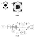
FIG. 1 shows the simulation result of the far field optical intensity distributions of the same diffractive optical element working at two different wavelengths. -
FIG. 2 shows the schematic of the detection apparatus used to test the optical performance of a diffractive optical element. - Additional descriptions of the invention are presented combining with the drawings and embodiment. These descriptions are not the limitation of the protection range for the invention.
- In
Fig. 1 , the annular far field optical intensity distribution generated by a beam shaping element in an ultraviolet lithography machine is shown as an example. As the result of the simulation, when the wavelength of input light source changes, the far field optical intensity distribution will change. For example, at wavelength λ=248 nm, the far field optical intensity distribution of the diffractive optical element is an annular distribution shown as 101. Its outside diameter is D=20 mm. The aperture size of the diffractive optical element is 10 mmx10 mm. Based on the computer simulation, it can be found that when the input beam wavelength is changed to λ'=Mλ (M>1), the outside diameter of the far fieldoptical intensity distribution 102 enlarges M times, while its shape does not change. Moreover, in the middle of the far field optical intensity distribution, a strong light spot appears. By the principle of Fraunhofer diffraction theorem, if we neglect the refractive index change at the different wavelength (the change is very small usually), the outside dimension D of the far field optical intensity distribution is proportional to wavelength λ (Yu Daoyin, Tan Hengying, Engineering Optics (Second Edition), Mechanical Industry Press, 2005, P345, in Chinese):
- Therefore, it is proved by the simulation result and theoretical analysis that testing the optical performance of a diffractive optical element at the wavelength different from its working wavelength is practicable. This is the basis of this invention. In the testing process of this invention, the central light spot should be blocked. Because the intensity of this light spot is too high to saturate and can even destroy the CCD. After the central obscuration is installed before the CCD, the far field optical intensity distribution is measured by the CCD imaging camera. Finally, the far field optical intensity distribution at the ultraviolet wavelength is received by shrinking the measured distribution at the ratio of λ'/λ, wherein λ' is the visible wavelength used in the measurement, and λ is the ultraviolet working wavelength.
- The equations used for energy efficiency test are deduced in the following:
- The diffractive optical element is used for beam shaping, and it is a phase grating consisting of multiple step-like reliefs. The intensity of every diffractive order is (Yu Daoyin, Tan Hengying, Engineering Optics (Second Edition), Mechanical Industry Press, 2005, P366, in Chinese):

- As indicated in this equation, when the input laser wavelength is changed, the intensity of each diffractive order will change correspondingly. In general, the diffractive optical element is designed in accordance with 2π phase difference, which means h=λ/(n-1), λ is the working wavelength of diffractive optical element. However, in actual fabrication process, there is small deviation Δh to the step height h due to the fabrication error. For the diffractive optical element, useful energy is concentrated in the first-order diffraction, which means m=1.
- Based on the above equation, at the working wavelength λ, the first-order energy efficiency can be expressed by:

- At the testing wavelength λ', the first-order energy efficiency can be expressed by:


-
Fig. 2 shows a detection apparatus for testing optical performance of a diffractive optical element. This apparatus comprises avisible wavelength laser 201 and other optical units placed along the optical axis including, in order from the side of thelaser 201, a beamexpander lens group 202, abeam splitter 203, first farfield imaging lens 206, anadjustable aperture 208, a second farfield imaging lens 209 and asecond energy sensor 210. - In the apparatus, the
beam splitter 203 is 45° to the optical axis. At the reflection direction of thebeam splitter 203, there is afirst energy sensor 204 to detect the input beam energy. - The diffractive optical element to be tested 205 is located at the object focal plane of the first far
field imaging lens 206. The focal length of both the first farfield imaging lens 206 and the second far field imaging lens 207 is f. The distance between the first farfield imaging lens 206 and the second far field imaging lens 207 is 2f. Thesecond energy sensor 210 is located at the image focal plane of the second farfield imaging lens 209. - At the common focal plane of the first far
field imaging lens 206 and the second farfield imaging lens 209, there is theadjustable aperture 208 or the CCD image sensor 207-2. In the middle of photosensitive surface of the CCD image sensor 207-2, there is a central obscuration 207-1. - At the object focal plane of the first far
field imaging lens 206, there has an adjustable frame to fix the diffractiveoptical element 205. - At the common focal plane of the first far
field imaging lens 206 and the second farfield imaging lens 209 there is an interchange unit to control the exchange of said CCD image sensor 207-2 (containing said central obscuration 207-1) and saidadjustable aperture 208. When said interchange unit is working, said CCD image sensor 207-2 and saidadjustable aperture 208 will change their position, and one of the two components is located along the optical axis of the optical path, the other one is outside the optical path. - The embodiment is shown in the following to describe the whole detection apparatus components, light path construction and detection method.
- First, a
visible wavelength laser 201 such as 632.8 nm He-Ne laser is chosen. The laser outside diameter is about 0.5 mm. Abeam expander 202 is located after the laser to expand the laser beam diameter to at least the aperture of diffractiveoptical element 205 about 14.14 mm, which is the diameter of the diagonal calculated by
optical element 205. Abeam splitter 203 is a half transmission and half reflection mirror. The half transmission light was detected by thefirst energy sensor 204, whose detection diameter should be bigger than 14.14 mm, while the half reflection light was vertically illuminated on the diffractiveoptical element 205. The above light path is shared, while subsequent light path has two cases: the "A" light path is used to test the far field optical intensity distribution; the "B" light path is used to test the energy efficiency. Two cases are described separately bellow. - In the "A" light path, a 2-f measurement system to test the far field light intensity distribution of the diffractive optical element is used. The 2-f measurement system comprises: the diffractive
optical element 205 located at the object focal plane of the first farfield imaging lens 206, and the CCD image sensor 207-2 located at the image focal plane of the first farfield imaging lens 206. In order to ensure the far field imaging to be fully detected by the CCD image sensor 207-2, the focal length of the first farfield imaging lens 206 should be carefully chosen according to CCD size of the CCD image sensor 207-2 based on the equation:
optical element 205. On the other hand, according to the diffraction law, NA is dependent with the lateral size of the phase step of the diffractiveoptical element 205 and the laser wavelength λ:
field imaging lens 206 should satisfy:
- In the embodiment, the CCD size l is 12 mm, the laser wavelength is 632.8 nm, and the lateral size of the phase step d is 5 µm. According to the equation, f can be chosen as 40 mm.
- In
FIG. 2 , in the middle of photosensitive surface of the CCD image sensor 207-2, there is a central obscuration 207-1 to block the central light spot. The area ratio of the central obscuration to the CCD photosensitive area should be less than 0.05. In this embodiment, a 0.5 mm diameter round central obscuration is used. - The test procedure of the far field optical intensity distribution is as following:
- ① The CCD image sensor together with the central obscuration is located at the optical path by using the interchange unit.
- ② The visible wavelength laser is turned on, followed by the beam expander lens group adjustment to expand the output beam of the visible wavelength laser to the same dimension as the aperture of the diffractive optical element 14.14 mm (the diameter of the diagonal is 10 mm×√2). In the following, the beam passed square aperture is to be size of 10 mmx10 mm. After the
beam splitter 203 is used to split the beam into reflection beam and transmission beam, the transmission beam is illuminated on the diffractiveoptical element 205, and then the far field optical intensity distribution is detected by the CCD image sensor 207-2. - ③ The size of far field distribution at ultraviolet working wavelength (λ) is shrunk by the ratio of λ'/λ. The working wavelength of diffractive optical element is 248 nm, so the shrink ration is 2.55. The reduced far field optical intensity distribution is the far field optical intensity distribution at ultraviolet working wavelength.
- In
FIG. 2 , the "B" light path is used to test the energy efficiency of the diffractiveoptical element 205. In the "B" light path, a 4-f measurement system is applied as: the first farfield imaging lens 206 and the second farfield imaging lens 209 are located in the light beam; the diffractiveoptical element 205 is located at the object focal plane of the first farfield imaging lens 206; theadjustable aperture 208 is located at the image focal plane of the first farfield imaging lens 206 and object focal plane of the second farfield imaging lens 209; thesecond energy sensor 210 is located at the image focal plane of the second farfield imaging lens 209. The focal lengths f of the two far field imaging lenses are the same. The distance from the diffractiveoptical element 205 to thesecond energy sensor 210 is 4f. This is the reason why this optical path called 4f measurement system. Theadjustable aperture 208 is in the same position of the CCD image sensor 207-2 in "A" light path. The focal length of the first farfield imaging lens 206 is the same as that in "A" light path. - The test procedure of energy efficiency is as following:
- ① The
adjustable aperture 208 is located at the optical path by using the interchange unit. - ② The
visible wavelength laser 201 is turned on, followed by the beamexpander lens group 202 adjustment to expand the output beam of the visible wavelength laser to the same dimension as the aperture of the diffractive optical element 14.14 mm (the diameter of the diagonal is 10
beam splitter 203 is used to split the beam into reflection beam and transmission beam. The transmission light is illuminated on the diffractiveoptical element 205. - ③ Measurement of zeroth-order diffractive efficiency at visible wavelength The
adjustable aperture 208 is turned to its minimum size (in this embodiment is 0.3 mm) to only let the central light pass. After passing through thebeam expander 202 and reflected by thebeam splitter 203, the laser was detected by thefirst energy sensor 204 to measure the input laser beam energy I in. The transmission beam from thebeam splitter 203, illuminating on the diffractiveoptical element 205, subsequently passing through the first farfield imaging lens 206, and finally theadjustable aperture 208 and the second farfield imaging lens 209, is detected by the second energy sensor to measure the zeroth-order light intensity I0 '. The zeroth-order diffraction energy efficiency is calculated by η 0'= I0 /Iin . - 4) Calculation of the phase number N of the diffractive optical element by using the equation:

- 5) Measurement of first-order diffractive efficiency at visible wavelength (λ')
Theadjustable aperture 208 is turned to the size same as that of the far field distribution D'. The zeroth-order and first-order light intensity I 0+1 ' is measured by thesecond energy sensor 210, and at the same time the input light intensity Iin is measured by thefirst energy sensor 204. The first-order diffractive efficiency η 1' is calculated by the equation:
- 6) first-order diffractive efficiency (η 1) of the diffractive optical element at the ultraviolet working wavelength (λ) is calculated by

- Test wavelength selection should follow the following principles: test wavelength λ' should be longer than the working ultraviolet wavelength λ, and λ'/λ is preferred to be 2∼4. Because from the above equation, when λ'/λ=4, we can get η 1'/η 1=0.09, which means the ratio of the two energy efficiencies is higher than 10. The reliability of the measurements is close to its limitation.
- It is a feature of this invention that visible light is used to test the optical performance of a diffractive optical element suitable for use in an ultraviolet lithography illumination system to detect its far field optical intensity distribution and energy efficiency. This invention has additional features such as low cost, easy operation and quick measurement.
Claims (5)
- A detection apparatus for testing optical performance of a diffractive optical element suitable for use in an ultraviolet lithography machine comprising a visible wavelength laser (201) and the following optical units placed along the laser direction and along the optical axis of the laser in the following sequence: a beam expander lens group (202), a beam splitter (203), a first far field imaging lens (206), an adjustable aperture (208) or a CCD image sensor (207-2), a second far field imaging lens (209) and a second energy sensor (210),
wherein said beam splitter (203) has an angle of 45° to said optical axis, and at the reflection direction of the beam splitter (203) there is a first energy sensor (204),
wherein the diffractive optical element (205) is located at the object focal plane of said first far field imaging lens (206), the object and image focal lengths of both said first far field imaging lens (206) and said second far field imaging lens (209) are f, the distance between said first far field imaging lens (206) and said second far field imaging lens (209) is 2f, and said second energy sensor (210) is located at the image focal plane of said second far field imaging lens (209),
wherein at the common focal plane of said first far field imaging lens (206) and said second far field imaging lens (209), there is said adjustable aperture (208) or said CCD image sensor (207-2), and in the middle of photosensitive surface of said CCD image sensor (207-2) ,there is a central obscuration (207-1). - The detection apparatus for testing optical performance of a diffractive optical element according to claim 1, wherein at the object focal plane of said first far field imaging lens (206) there exists an adjustable frame to install said diffractive optical element (205).
- The detection apparatus for testing optical performance of a diffractive optical element according to claim 1, wherein at the common focal plane of said first far field imaging lens (206) and said second far field imaging lens (209), there is an interchange unit to control the exchange of said CCD image sensor (207-2) containing said central obscuration (207-1) and said adjustable aperture (208), when said interchange unit works, said CCD image sensor (207-2) and said adjustable aperture (208) change their position, and one of the two components is located along the optical axis of the optical path, the other one is outside the optical path.
- The detection apparatus for testing optical performance of a diffractive optical element according to claim 1, wherein said beam splitter (203) is a half transmission and half reflection mirror.
- A detection method using the detection apparatus for testing optical performance of a diffractive optical element according to claim 1 comprising in the listed sequence1) Detection of far field optical intensity distribution① placing said CCD image sensor (207-2) at the optical path by using said interchange unit,② turning on said visible wavelength laser (201), adjusting the beam expander lens group (202) to expand the output beam of said visible wavelength laser (201) to the same dimension as that of the aperture of said diffractive optical element (205); wherein the beam passes square pinhole aperture and said beam splitter (203), and splits into reflection beam and transmission beam; said transmission beam is illuminated on said diffractive optical element (205), and then the far field optical intensity distribution is detected by said CCD image sensor (207-2) and the optical far field distribution size D' is determined:
 ③ determining the size of far field distribution at ultraviolet working wavelength (λ) having the relationship with that at visible wavelength by
 2) Detection of energy efficiency:① measuring zeroth-order diffractive efficiency at visible wavelength (λ'), wherein
said adjustable aperture (208) is turned to its minimum size to only let zeroth-order diffractive light pass, the zeroth-order light intensity I0 ' is measured by said second energy sensor (210), and at the same time the input light intensity Iin is measured by said first energy sensor (204), and the phase number N of said diffractive optical element (205) is calculated by the equation: ② measuring first-order diffractive efficiency at visible wavelength (λ'), wherein
said adjustable aperture (208) is turned to the size as same as that of said far field distribution D', the zeroth-order and first-order light intensity I 0+1 ' is measured by said second energy sensor (210), and at the same time the input light intensity Iin is measured by said first energy sensor (204). first-order diffractive efficiency η 1' is calculated by the equation: ③ calculating first-order diffractive efficiency (η 1) of said diffractive optical element (205) at said ultraviolet working wavelength (λ) by
Applications Claiming Priority (2)
| Application Number | Priority Date | Filing Date | Title |
|---|---|---|---|
| CN2011101672360A CN102243137B (en) | 2011-06-21 | 2011-06-21 | Detection device and detection method for optical performance of beam shaping element |
| PCT/CN2011/001063 WO2012174683A1 (en) | 2011-06-21 | 2011-06-28 | Device and method for detecting optical performance of beam shaping element |
Publications (3)
| Publication Number | Publication Date |
|---|---|
| EP2562526A1 EP2562526A1 (en) | 2013-02-27 |
| EP2562526A4 EP2562526A4 (en) | 2014-08-13 |
| EP2562526B1 true EP2562526B1 (en) | 2016-10-19 |
Family
ID=44961305
Family Applications (1)
| Application Number | Title | Priority Date | Filing Date |
|---|---|---|---|
| EP11838977.4A Active EP2562526B1 (en) | 2011-06-21 | 2011-06-28 | Device and method for detecting optical performance of beam shaping element |
Country Status (4)
| Country | Link |
|---|---|
| US (1) | US9121788B2 (en) |
| EP (1) | EP2562526B1 (en) |
| CN (1) | CN102243137B (en) |
| WO (1) | WO2012174683A1 (en) |
Families Citing this family (29)
| Publication number | Priority date | Publication date | Assignee | Title |
|---|---|---|---|---|
| CN102528293A (en) * | 2012-01-11 | 2012-07-04 | 广东省南方彩色制版有限公司 | Depth-adjustable femtosecond laser punching device for printing stencils |
| CN102636272B (en) * | 2012-03-22 | 2013-11-20 | 中国科学院上海光学精密机械研究所 | Femtosecond laser pulse measurement method based on transient grating effect and device |
| CN102628996B (en) * | 2012-03-31 | 2014-03-26 | 北京国科世纪激光技术有限公司 | Fundamental transverse mode laser beam shaping device and method |
| CN102735428B (en) * | 2012-06-08 | 2014-10-01 | 中国科学院上海光学精密机械研究所 | Measuring device and method for optical performance of diffractive optical element |
| EP2878402A1 (en) * | 2013-12-02 | 2015-06-03 | SLM Solutions Group AG | Apparatus and method for producing three-dimensional work pieces with a radiation detection device |
| TWI491856B (en) | 2014-06-20 | 2015-07-11 | Univ Nat Central | Detecting system |
| US9625726B2 (en) * | 2014-12-05 | 2017-04-18 | Kla-Tencor Corp. | Lens array-based illumination for wafer inspection |
| CN105511085B (en) * | 2015-11-10 | 2019-03-08 | 河南中光学集团有限公司 | A kind of laser beam expanding fusion optical system |
| CN107186336B (en) * | 2016-03-09 | 2021-08-27 | 住友重机械工业株式会社 | Laser processing apparatus |
| CN107064907A (en) * | 2017-03-07 | 2017-08-18 | 北京环境特性研究所 | A kind of laser beam emitting device of new LRCS test systems |
| CN109387353B (en) * | 2017-08-14 | 2021-07-23 | 深圳光峰科技股份有限公司 | Microlens array detection system and microlens array detection method |
| CN107860713B (en) * | 2017-11-06 | 2020-12-15 | 湖北工程学院 | Spectral stability optimization device, system and method |
| CN109141825B (en) * | 2018-09-13 | 2019-07-02 | 西华大学 | Subwavelength optical imaging device focal length measuring device and measuring method |
| WO2020064108A1 (en) * | 2018-09-27 | 2020-04-02 | MAX-PLANCK-Gesellschaft zur Förderung der Wissenschaften e.V. | Method of and apparatus for forming and shifting a light intensity distribution in a focal area of an objective lens |
| CN109342028A (en) * | 2018-10-17 | 2019-02-15 | 深圳奥比中光科技有限公司 | Diffractive optical element detection method and system |
| CN110146991B (en) * | 2019-04-18 | 2024-07-09 | 珠海市运泰利自动化设备有限公司 | Laser spot shaping optical system |
| CN110202265A (en) * | 2019-05-14 | 2019-09-06 | 中国电子科技集团公司第三十八研究所 | A kind of processing method of diamond high-precision microchanneled surface |
| CN111735613A (en) * | 2020-08-11 | 2020-10-02 | 吉林省春曦光电科技有限公司 | Optical Quality Inspection System of Four Quadrant Detector Lenses |
| CN112414677B (en) * | 2020-11-10 | 2022-05-27 | 中国工程物理研究院上海激光等离子体研究所 | Testing device and method for measuring size of light spot in optical element body with high precision |
| CN112697284A (en) * | 2020-12-08 | 2021-04-23 | 中国人民解放军空军工程大学 | Remote laser light field pulse waveform distribution characteristic measurement system |
| CN112630983A (en) * | 2020-12-24 | 2021-04-09 | 中国工程物理研究院激光聚变研究中心 | Laser system, laser-induced damage testing system and method |
| CN112987528B (en) * | 2021-03-08 | 2022-03-22 | 昆明理工大学 | Method for realizing edge extraction of annular light based on 4f system |
| CN113267840B (en) * | 2021-05-08 | 2022-02-22 | 中国工程物理研究院激光聚变研究中心 | Sawtooth diaphragm, application thereof and debugging method of sawtooth diaphragm to light path |
| CN113639965B (en) * | 2021-07-30 | 2023-01-17 | 中国科学院空天信息创新研究院 | A spectral resolution acquisition method for a single-lens spectroscopic device |
| CN113945364A (en) * | 2021-10-25 | 2022-01-18 | 中国科学院光电技术研究所 | Device and method for measuring diffraction efficiency of diffractive optical element |
| CN114640419A (en) * | 2022-03-01 | 2022-06-17 | 北京交通大学 | Optical fiber mode decomposition device based on optical tomography |
| CN115165314A (en) * | 2022-06-23 | 2022-10-11 | 深圳市先地图像科技有限公司 | Laser light source detection device |
| CN117347015B (en) * | 2023-12-06 | 2024-02-20 | 中国航天三江集团有限公司 | High-energy laser beam quality outfield high-precision measurement method and system |
| CN119916578A (en) * | 2025-01-26 | 2025-05-02 | 皖江新兴产业技术发展中心 | A new type of laser-driven plasma light source |
Family Cites Families (17)
| Publication number | Priority date | Publication date | Assignee | Title |
|---|---|---|---|---|
| JPH0396813A (en) * | 1989-09-11 | 1991-04-22 | Ya Man Ltd | Portable photoelectric displacement measuring instrument |
| JPH07234171A (en) * | 1994-02-24 | 1995-09-05 | Fuji Photo Optical Co Ltd | Reflection efficiency measuring instrument and diffraction efficiency measuring instrument |
| JP3334470B2 (en) * | 1996-01-17 | 2002-10-15 | 松下電器産業株式会社 | Diffraction efficiency measurement method and diffraction efficiency measurement device |
| TW482705B (en) * | 1999-05-28 | 2002-04-11 | Electro Scient Ind Inc | Beam shaping and projection imaging with solid state UV Gaussian beam to form blind vias |
| TW550377B (en) | 2000-02-23 | 2003-09-01 | Zeiss Stiftung | Apparatus for wave-front detection |
| JP3578144B2 (en) * | 2002-01-16 | 2004-10-20 | 住友電気工業株式会社 | Apparatus and method for measuring optical characteristics of diffractive optical parts |
| JP2005268035A (en) * | 2004-03-18 | 2005-09-29 | Canon Inc | Evaluation apparatus for evaluation of EUV light source and evaluation method using the same |
| JP4522137B2 (en) * | 2004-05-07 | 2010-08-11 | キヤノン株式会社 | Optical system adjustment method |
| US20050259269A1 (en) | 2004-05-19 | 2005-11-24 | Asml Holding N.V. | Shearing interferometer with dynamic pupil fill |
| US7259869B2 (en) * | 2004-06-29 | 2007-08-21 | Kla-Tencor Technologies Corporation | System and method for performing bright field and dark field optical inspection |
| CN100378442C (en) * | 2004-06-30 | 2008-04-02 | 中国科学院上海光学精密机械研究所 | Optical wave front detection device and detection method thereof |
| JP2006279017A (en) | 2005-03-02 | 2006-10-12 | Canon Inc | Exposure apparatus and method, measuring apparatus, and device manufacturing method |
| CN100445718C (en) * | 2005-05-18 | 2008-12-24 | 中国科学院长春光学精密机械与物理研究所 | Measuring method and device of optical transfer function |
| US9239455B2 (en) * | 2007-12-31 | 2016-01-19 | Stc.Unm | Structural illumination and evanescent coupling for the extension of imaging interferometric microscopy |
| US9151719B2 (en) * | 2011-12-27 | 2015-10-06 | Hitachi High-Technologies Corporation | Inspection apparatus |
| CN102735428B (en) * | 2012-06-08 | 2014-10-01 | 中国科学院上海光学精密机械研究所 | Measuring device and method for optical performance of diffractive optical element |
| DE102013016368B4 (en) * | 2013-09-30 | 2024-05-16 | Carl Zeiss Microscopy Gmbh | Light microscope and microscopy method for examining a microscopic sample |
-
2011
- 2011-06-21 CN CN2011101672360A patent/CN102243137B/en active Active
- 2011-06-28 EP EP11838977.4A patent/EP2562526B1/en active Active
- 2011-06-28 WO PCT/CN2011/001063 patent/WO2012174683A1/en not_active Ceased
- 2011-06-28 US US14/125,581 patent/US9121788B2/en active Active
Also Published As
| Publication number | Publication date |
|---|---|
| WO2012174683A1 (en) | 2012-12-27 |
| US9121788B2 (en) | 2015-09-01 |
| CN102243137A (en) | 2011-11-16 |
| CN102243137B (en) | 2013-04-10 |
| EP2562526A4 (en) | 2014-08-13 |
| EP2562526A1 (en) | 2013-02-27 |
| US20140132952A1 (en) | 2014-05-15 |
Similar Documents
| Publication | Publication Date | Title |
|---|---|---|
| EP2562526A1 (en) | Device and method for detecting optical performance of beam shaping element | |
| TWI574116B (en) | Inspection apparatus, lithographic apparatus, and device manufacturing method | |
| US7548077B2 (en) | Measuring apparatus and a measuring method for measuring a polarization characteristic of an optical system | |
| TW446814B (en) | Image quality mapper for progressive eyeglasses and method for measuring said image quality | |
| TWI569002B (en) | Precision measuring tools, catadioptric optical systems, and precision measuring methods | |
| CN102494873B (en) | Method for measuring focal length of micro-lens array | |
| CN101495833A (en) | Optical element and method of calibrating a measuring apparatus comprising a wave shaping structure | |
| JPH03183904A (en) | Detection of shape of object | |
| US20060164630A1 (en) | Method and measuring device for contactless measurement of angles or angle changes on objects | |
| CN100561359C (en) | Asymmetric Phase-Shifting Grating Marking and Its Application in Object Mirror Aberration Detection of Lithography Machine | |
| NL1032952C2 (en) | Polarization evaluation mask, polarization evaluation method and polarization determining device. | |
| CN103076724B (en) | Projection objective wave aberration on-line detection device and method based on double-beam interference | |
| US5548401A (en) | Photomask inspecting method and apparatus | |
| Xu et al. | Rotatable single wedge plate shearing interference technique for collimation testing | |
| US5661560A (en) | Elliptical light measuring method | |
| CN100378442C (en) | Optical wave front detection device and detection method thereof | |
| US12019231B2 (en) | Device for analyzing size of step in pair of divided mirrors of telescope | |
| US6081333A (en) | Bi-lateral shearing interferometer with beam convergence/divergence indication | |
| WO2025021452A1 (en) | Systems and methods for non-linear optical metrology for advanced sub-diffraction imaging | |
| Lindlein et al. | Optical measurement methods for refractive microlenses and arrays | |
| Xu | Any-orientation shear-plate tester by two rotating ways | |
| Chen | Optical axis alignment for three-aspherical mirrors system using five parallel laser beams and moiré method | |
| Miks et al. | Influence of material dispersion on the measurement accuracy of chromatic sensors | |
| Kanzler et al. | High aspect ratio line shapes generated with a diffractive/refractive hybrid approach | |
| Blattner et al. | Optical measurement of the global and local geometry of grating structures |
Legal Events
| Date | Code | Title | Description |
|---|---|---|---|
| PUAI | Public reference made under article 153(3) epc to a published international application that has entered the european phase |
Free format text: ORIGINAL CODE: 0009012 |
|
| 17P | Request for examination filed |
Effective date: 20121023 |
|
| AK | Designated contracting states |
Kind code of ref document: A1 Designated state(s): AL AT BE BG CH CY CZ DE DK EE ES FI FR GB GR HR HU IE IS IT LI LT LU LV MC MK MT NL NO PL PT RO RS SE SI SK SM TR |
|
| A4 | Supplementary search report drawn up and despatched |
Effective date: 20140716 |
|
| RIC1 | Information provided on ipc code assigned before grant |
Ipc: G01M 11/02 20060101AFI20140710BHEP Ipc: G02B 27/10 20060101ALI20140710BHEP Ipc: G02B 27/09 20060101ALI20140710BHEP Ipc: G03F 7/20 20060101ALI20140710BHEP |
|
| DAX | Request for extension of the european patent (deleted) | ||
| REG | Reference to a national code |
Ref country code: DE Ref legal event code: R079 Ref document number: 602011031560 Country of ref document: DE Free format text: PREVIOUS MAIN CLASS: G01M0011020000 Ipc: G03F0007200000 |
|
| GRAP | Despatch of communication of intention to grant a patent |
Free format text: ORIGINAL CODE: EPIDOSNIGR1 |
|
| RIC1 | Information provided on ipc code assigned before grant |
Ipc: G03F 7/20 20060101AFI20160504BHEP Ipc: G02B 19/00 20060101ALI20160504BHEP Ipc: B23K 26/70 20140101ALI20160504BHEP |
|
| INTG | Intention to grant announced |
Effective date: 20160527 |
|
| GRAS | Grant fee paid |
Free format text: ORIGINAL CODE: EPIDOSNIGR3 |
|
| GRAA | (expected) grant |
Free format text: ORIGINAL CODE: 0009210 |
|
| AK | Designated contracting states |
Kind code of ref document: B1 Designated state(s): AL AT BE BG CH CY CZ DE DK EE ES FI FR GB GR HR HU IE IS IT LI LT LU LV MC MK MT NL NO PL PT RO RS SE SI SK SM TR |
|
| REG | Reference to a national code |
Ref country code: GB Ref legal event code: FG4D |
|
| REG | Reference to a national code |
Ref country code: CH Ref legal event code: EP |
|
| REG | Reference to a national code |
Ref country code: AT Ref legal event code: REF Ref document number: 838830 Country of ref document: AT Kind code of ref document: T Effective date: 20161115 |
|
| REG | Reference to a national code |
Ref country code: IE Ref legal event code: FG4D Ref country code: NL Ref legal event code: FP |
|
| REG | Reference to a national code |
Ref country code: DE Ref legal event code: R096 Ref document number: 602011031560 Country of ref document: DE |
|
| REG | Reference to a national code |
Ref country code: LT Ref legal event code: MG4D |
|
| PG25 | Lapsed in a contracting state [announced via postgrant information from national office to epo] |
Ref country code: LV Free format text: LAPSE BECAUSE OF FAILURE TO SUBMIT A TRANSLATION OF THE DESCRIPTION OR TO PAY THE FEE WITHIN THE PRESCRIBED TIME-LIMIT Effective date: 20161019 |
|
| REG | Reference to a national code |
Ref country code: AT Ref legal event code: MK05 Ref document number: 838830 Country of ref document: AT Kind code of ref document: T Effective date: 20161019 |
|
| PG25 | Lapsed in a contracting state [announced via postgrant information from national office to epo] |
Ref country code: NO Free format text: LAPSE BECAUSE OF FAILURE TO SUBMIT A TRANSLATION OF THE DESCRIPTION OR TO PAY THE FEE WITHIN THE PRESCRIBED TIME-LIMIT Effective date: 20170119 Ref country code: GR Free format text: LAPSE BECAUSE OF FAILURE TO SUBMIT A TRANSLATION OF THE DESCRIPTION OR TO PAY THE FEE WITHIN THE PRESCRIBED TIME-LIMIT Effective date: 20170120 Ref country code: SE Free format text: LAPSE BECAUSE OF FAILURE TO SUBMIT A TRANSLATION OF THE DESCRIPTION OR TO PAY THE FEE WITHIN THE PRESCRIBED TIME-LIMIT Effective date: 20161019 Ref country code: LT Free format text: LAPSE BECAUSE OF FAILURE TO SUBMIT A TRANSLATION OF THE DESCRIPTION OR TO PAY THE FEE WITHIN THE PRESCRIBED TIME-LIMIT Effective date: 20161019 |
|
| PG25 | Lapsed in a contracting state [announced via postgrant information from national office to epo] |
Ref country code: IS Free format text: LAPSE BECAUSE OF FAILURE TO SUBMIT A TRANSLATION OF THE DESCRIPTION OR TO PAY THE FEE WITHIN THE PRESCRIBED TIME-LIMIT Effective date: 20170219 Ref country code: BE Free format text: LAPSE BECAUSE OF FAILURE TO SUBMIT A TRANSLATION OF THE DESCRIPTION OR TO PAY THE FEE WITHIN THE PRESCRIBED TIME-LIMIT Effective date: 20161019 Ref country code: PT Free format text: LAPSE BECAUSE OF FAILURE TO SUBMIT A TRANSLATION OF THE DESCRIPTION OR TO PAY THE FEE WITHIN THE PRESCRIBED TIME-LIMIT Effective date: 20170220 Ref country code: HR Free format text: LAPSE BECAUSE OF FAILURE TO SUBMIT A TRANSLATION OF THE DESCRIPTION OR TO PAY THE FEE WITHIN THE PRESCRIBED TIME-LIMIT Effective date: 20161019 Ref country code: FI Free format text: LAPSE BECAUSE OF FAILURE TO SUBMIT A TRANSLATION OF THE DESCRIPTION OR TO PAY THE FEE WITHIN THE PRESCRIBED TIME-LIMIT Effective date: 20161019 Ref country code: ES Free format text: LAPSE BECAUSE OF FAILURE TO SUBMIT A TRANSLATION OF THE DESCRIPTION OR TO PAY THE FEE WITHIN THE PRESCRIBED TIME-LIMIT Effective date: 20161019 Ref country code: PL Free format text: LAPSE BECAUSE OF FAILURE TO SUBMIT A TRANSLATION OF THE DESCRIPTION OR TO PAY THE FEE WITHIN THE PRESCRIBED TIME-LIMIT Effective date: 20161019 Ref country code: RS Free format text: LAPSE BECAUSE OF FAILURE TO SUBMIT A TRANSLATION OF THE DESCRIPTION OR TO PAY THE FEE WITHIN THE PRESCRIBED TIME-LIMIT Effective date: 20161019 Ref country code: AT Free format text: LAPSE BECAUSE OF FAILURE TO SUBMIT A TRANSLATION OF THE DESCRIPTION OR TO PAY THE FEE WITHIN THE PRESCRIBED TIME-LIMIT Effective date: 20161019 |
|
| REG | Reference to a national code |
Ref country code: FR Ref legal event code: PLFP Year of fee payment: 7 |
|
| REG | Reference to a national code |
Ref country code: DE Ref legal event code: R097 Ref document number: 602011031560 Country of ref document: DE |
|
| PG25 | Lapsed in a contracting state [announced via postgrant information from national office to epo] |
Ref country code: RO Free format text: LAPSE BECAUSE OF FAILURE TO SUBMIT A TRANSLATION OF THE DESCRIPTION OR TO PAY THE FEE WITHIN THE PRESCRIBED TIME-LIMIT Effective date: 20161019 Ref country code: SK Free format text: LAPSE BECAUSE OF FAILURE TO SUBMIT A TRANSLATION OF THE DESCRIPTION OR TO PAY THE FEE WITHIN THE PRESCRIBED TIME-LIMIT Effective date: 20161019 Ref country code: EE Free format text: LAPSE BECAUSE OF FAILURE TO SUBMIT A TRANSLATION OF THE DESCRIPTION OR TO PAY THE FEE WITHIN THE PRESCRIBED TIME-LIMIT Effective date: 20161019 Ref country code: DK Free format text: LAPSE BECAUSE OF FAILURE TO SUBMIT A TRANSLATION OF THE DESCRIPTION OR TO PAY THE FEE WITHIN THE PRESCRIBED TIME-LIMIT Effective date: 20161019 Ref country code: CZ Free format text: LAPSE BECAUSE OF FAILURE TO SUBMIT A TRANSLATION OF THE DESCRIPTION OR TO PAY THE FEE WITHIN THE PRESCRIBED TIME-LIMIT Effective date: 20161019 |
|
| PGFP | Annual fee paid to national office [announced via postgrant information from national office to epo] |
Ref country code: FR Payment date: 20170625 Year of fee payment: 7 |
|
| PLBE | No opposition filed within time limit |
Free format text: ORIGINAL CODE: 0009261 |
|
| STAA | Information on the status of an ep patent application or granted ep patent |
Free format text: STATUS: NO OPPOSITION FILED WITHIN TIME LIMIT |
|
| PG25 | Lapsed in a contracting state [announced via postgrant information from national office to epo] |
Ref country code: SM Free format text: LAPSE BECAUSE OF FAILURE TO SUBMIT A TRANSLATION OF THE DESCRIPTION OR TO PAY THE FEE WITHIN THE PRESCRIBED TIME-LIMIT Effective date: 20161019 Ref country code: BG Free format text: LAPSE BECAUSE OF FAILURE TO SUBMIT A TRANSLATION OF THE DESCRIPTION OR TO PAY THE FEE WITHIN THE PRESCRIBED TIME-LIMIT Effective date: 20170119 Ref country code: IT Free format text: LAPSE BECAUSE OF FAILURE TO SUBMIT A TRANSLATION OF THE DESCRIPTION OR TO PAY THE FEE WITHIN THE PRESCRIBED TIME-LIMIT Effective date: 20161019 |
|
| 26N | No opposition filed |
Effective date: 20170720 |
|
| PG25 | Lapsed in a contracting state [announced via postgrant information from national office to epo] |
Ref country code: SI Free format text: LAPSE BECAUSE OF FAILURE TO SUBMIT A TRANSLATION OF THE DESCRIPTION OR TO PAY THE FEE WITHIN THE PRESCRIBED TIME-LIMIT Effective date: 20161019 |
|
| PG25 | Lapsed in a contracting state [announced via postgrant information from national office to epo] |
Ref country code: MC Free format text: LAPSE BECAUSE OF FAILURE TO SUBMIT A TRANSLATION OF THE DESCRIPTION OR TO PAY THE FEE WITHIN THE PRESCRIBED TIME-LIMIT Effective date: 20161019 |
|
| REG | Reference to a national code |
Ref country code: CH Ref legal event code: PL |
|
| GBPC | Gb: european patent ceased through non-payment of renewal fee |
Effective date: 20170628 |
|
| REG | Reference to a national code |
Ref country code: IE Ref legal event code: MM4A |
|
| PG25 | Lapsed in a contracting state [announced via postgrant information from national office to epo] |
Ref country code: GB Free format text: LAPSE BECAUSE OF NON-PAYMENT OF DUE FEES Effective date: 20170628 Ref country code: LU Free format text: LAPSE BECAUSE OF NON-PAYMENT OF DUE FEES Effective date: 20170628 Ref country code: LI Free format text: LAPSE BECAUSE OF NON-PAYMENT OF DUE FEES Effective date: 20170630 Ref country code: CH Free format text: LAPSE BECAUSE OF NON-PAYMENT OF DUE FEES Effective date: 20170630 Ref country code: IE Free format text: LAPSE BECAUSE OF NON-PAYMENT OF DUE FEES Effective date: 20170628 |
|
| PG25 | Lapsed in a contracting state [announced via postgrant information from national office to epo] |
Ref country code: MT Free format text: LAPSE BECAUSE OF NON-PAYMENT OF DUE FEES Effective date: 20170628 |
|
| PG25 | Lapsed in a contracting state [announced via postgrant information from national office to epo] |
Ref country code: FR Free format text: LAPSE BECAUSE OF NON-PAYMENT OF DUE FEES Effective date: 20180630 |
|
| PG25 | Lapsed in a contracting state [announced via postgrant information from national office to epo] |
Ref country code: HU Free format text: LAPSE BECAUSE OF FAILURE TO SUBMIT A TRANSLATION OF THE DESCRIPTION OR TO PAY THE FEE WITHIN THE PRESCRIBED TIME-LIMIT; INVALID AB INITIO Effective date: 20110628 |
|
| PG25 | Lapsed in a contracting state [announced via postgrant information from national office to epo] |
Ref country code: CY Free format text: LAPSE BECAUSE OF NON-PAYMENT OF DUE FEES Effective date: 20161019 |
|
| PG25 | Lapsed in a contracting state [announced via postgrant information from national office to epo] |
Ref country code: MK Free format text: LAPSE BECAUSE OF FAILURE TO SUBMIT A TRANSLATION OF THE DESCRIPTION OR TO PAY THE FEE WITHIN THE PRESCRIBED TIME-LIMIT Effective date: 20161019 |
|
| REG | Reference to a national code |
Ref country code: DE Ref legal event code: R082 Ref document number: 602011031560 Country of ref document: DE Representative=s name: SCHMID, MICHAEL, DIPL.-ING. UNIV., DE Ref country code: DE Ref legal event code: R081 Ref document number: 602011031560 Country of ref document: DE Owner name: BEIJING GUOWANG OPTICAL TECHNOLOGY CO., LTD., CN Free format text: FORMER OWNER: SHANGHAI INSTITUTE OF OPTICS AND FINE MECHANICS CHINESE ACADEMY OF SCIENCES, SHANGHAI, CN |
|
| PG25 | Lapsed in a contracting state [announced via postgrant information from national office to epo] |
Ref country code: TR Free format text: LAPSE BECAUSE OF FAILURE TO SUBMIT A TRANSLATION OF THE DESCRIPTION OR TO PAY THE FEE WITHIN THE PRESCRIBED TIME-LIMIT Effective date: 20161019 |
|
| REG | Reference to a national code |
Ref country code: NL Ref legal event code: PD Owner name: BEIJING GUOWANG OPTICAL TECHNOLOGY CO., LTD.; CN Free format text: DETAILS ASSIGNMENT: CHANGE OF OWNER(S), ASSIGNMENT; FORMER OWNER NAME: SHANGHAI INSTITUTE OF OPTICS AND FINE MECHANICS CHINESE ACADEMY OF SCIENCES Effective date: 20200401 |
|
| PG25 | Lapsed in a contracting state [announced via postgrant information from national office to epo] |
Ref country code: AL Free format text: LAPSE BECAUSE OF FAILURE TO SUBMIT A TRANSLATION OF THE DESCRIPTION OR TO PAY THE FEE WITHIN THE PRESCRIBED TIME-LIMIT Effective date: 20161019 |
|
| PGFP | Annual fee paid to national office [announced via postgrant information from national office to epo] |
Ref country code: NL Payment date: 20250528 Year of fee payment: 15 |
|
| PGFP | Annual fee paid to national office [announced via postgrant information from national office to epo] |
Ref country code: DE Payment date: 20250617 Year of fee payment: 15 |