EP2554720A1 - Method for synthesizing group ii-vi compound semiconductor polycrystals - Google Patents
Method for synthesizing group ii-vi compound semiconductor polycrystals Download PDFInfo
- Publication number
- EP2554720A1 EP2554720A1 EP11762541A EP11762541A EP2554720A1 EP 2554720 A1 EP2554720 A1 EP 2554720A1 EP 11762541 A EP11762541 A EP 11762541A EP 11762541 A EP11762541 A EP 11762541A EP 2554720 A1 EP2554720 A1 EP 2554720A1
- Authority
- EP
- European Patent Office
- Prior art keywords
- vessel
- pressure
- furnace
- compound semiconductor
- polycrystal
- Prior art date
- Legal status (The legal status is an assumption and is not a legal conclusion. Google has not performed a legal analysis and makes no representation as to the accuracy of the status listed.)
- Granted
Links
Images

Classifications
-
- C—CHEMISTRY; METALLURGY
- C22—METALLURGY; FERROUS OR NON-FERROUS ALLOYS; TREATMENT OF ALLOYS OR NON-FERROUS METALS
- C22C—ALLOYS
- C22C1/00—Making non-ferrous alloys
- C22C1/02—Making non-ferrous alloys by melting
-
- C—CHEMISTRY; METALLURGY
- C30—CRYSTAL GROWTH
- C30B—SINGLE-CRYSTAL GROWTH; UNIDIRECTIONAL SOLIDIFICATION OF EUTECTIC MATERIAL OR UNIDIRECTIONAL DEMIXING OF EUTECTOID MATERIAL; REFINING BY ZONE-MELTING OF MATERIAL; PRODUCTION OF A HOMOGENEOUS POLYCRYSTALLINE MATERIAL WITH DEFINED STRUCTURE; SINGLE CRYSTALS OR HOMOGENEOUS POLYCRYSTALLINE MATERIAL WITH DEFINED STRUCTURE; AFTER-TREATMENT OF SINGLE CRYSTALS OR A HOMOGENEOUS POLYCRYSTALLINE MATERIAL WITH DEFINED STRUCTURE; APPARATUS THEREFOR
- C30B11/00—Single-crystal growth by normal freezing or freezing under temperature gradient, e.g. Bridgman-Stockbarger method
- C30B11/002—Crucibles or containers for supporting the melt
-
- C—CHEMISTRY; METALLURGY
- C30—CRYSTAL GROWTH
- C30B—SINGLE-CRYSTAL GROWTH; UNIDIRECTIONAL SOLIDIFICATION OF EUTECTIC MATERIAL OR UNIDIRECTIONAL DEMIXING OF EUTECTOID MATERIAL; REFINING BY ZONE-MELTING OF MATERIAL; PRODUCTION OF A HOMOGENEOUS POLYCRYSTALLINE MATERIAL WITH DEFINED STRUCTURE; SINGLE CRYSTALS OR HOMOGENEOUS POLYCRYSTALLINE MATERIAL WITH DEFINED STRUCTURE; AFTER-TREATMENT OF SINGLE CRYSTALS OR A HOMOGENEOUS POLYCRYSTALLINE MATERIAL WITH DEFINED STRUCTURE; APPARATUS THEREFOR
- C30B29/00—Single crystals or homogeneous polycrystalline material with defined structure characterised by the material or by their shape
- C30B29/10—Inorganic compounds or compositions
- C30B29/46—Sulfur-, selenium- or tellurium-containing compounds
- C30B29/48—AIIBVI compounds wherein A is Zn, Cd or Hg, and B is S, Se or Te
Definitions
- the present invention relates to a method for synthesizing group II-VI compound semiconductor polycrystals as raw materials of group II-VI compound semiconductor single crystals, and particularly relates to a method for synthesizing CdTe family compound semiconductor polycrystal, particularly CdTe polycrystal.
- a compound semiconductor polycrystal has to be synthesized from a group II element and a group VI element at first for synthesizing a group II-VI compound semiconductor single crystal.
- a group II-VI compound semiconductor was synthesized by putting a group II single element and a group VI single element in a semi-airtight pBN inner vessel, sealing the inner vessel, setting the inner vessel in an airtight outer vessel of a quartz ampoule, vacuum sealing the outer vessel, and heating the outer vessel in an electric furnace up to a melting point or more so as to melt and react the raw elements.
- Patent Document 1 and Patent Document 2 disclose such a kind of synthesizing method of polycrystals.
- the quartz ampoule was disposed because a synthesized polycrystal has to be taken out by breaking the ampoule after synthesis. Thus it also causes difficulty to reduce the costs.
- a method for synthesizing group II-VI compound semiconductor polycrystals according to claim 1 includes steps of:
- the present invention provides a synthesizing method without using a quartz ampoule and contributes cost reduction by virtue of the reuse of a vessel.
- the invention of claim 2 is a method for synthesizing group II-VI compound semiconductor polycrystals of claim 1, in which the outer vessel is made of graphite and a surface of which is covered with a coating layer. It becomes easy to handle the outer vessel because the outer vessel is made of graphite. Also it becomes possible to restrict leakage of gasified raw materials from the outer vessel during heating by coating the surface of the outer vessel even when the vessel is made of graphite.
- the invention of claim 3 is a method for synthesizing group II-VI compound semiconductor polycrystals of claim 1 or 2, in which the inert gas pressure in the high-pressure furnace before heating is 0.5 MPa or more. It becomes possible to reduce leakage of gasified raw materials from the vessel during the heating by setting the inert gas pressure in the high-pressure furnace before heating at 0.5 MPa or more.
- the invention of claim 4 is a method for synthesizing group II-VI compound semiconductor polycrystals of claim 3, in which the group II-VI compound semiconductor polycrystal is a CdTe polycrystal, and a temperature raising rate at the heating step is 100 to 2000 degrees C per hour. It becomes possible to eliminate remaining of non-reacted materials and accomplish the synthesis of CdTe polycrystals completely by setting the temperature raising rate at the heating at 100 to 2000 degrees C per hour.
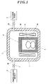
- FIG. 1 is a schematic structure of a device for synthesizing a group II-VI compound semiconductor polycrystal, such as a CdTe polycrystal, according to an embodiment of the present invention.
- a high-pressure furnace designated by symbol 1
- a vacuum pump 3 connected by piping 2a
- a pressurizing device 4 connected by piping 2b.
- the crystal synthesizing device is structured such that the high-pressure furnace 1 is evacuated by the vacuum pump 3 and the inner air is replaced with an inert gas such as a nitrogen gas (N2) through the piping 2b, and that an inert gas is filled with pressure by the pressurizing device 4 so as to control a pressure in the high-pressure furnace 1.
- an inert gas such as a nitrogen gas (N2)
- the pressurizing device 4 may include, for example, a high pressure gas-container.
- the pressure in the high-pressure furnace 1 may be set at a desirable pressure by introducing the gas into the furnace 1 from the high pressure gas-container via a pressure reducing valve and a pressure controller 5.
- a synthesis vessel 6 is placed around the center of the high-pressure furnace 1 and the vessel 6 is surrounded by a heater 7.
- the synthesis vessel 6 has a double-container structure of an inner vessel 6a and an outer vessel 6b.
- the inner vessel 6a is composed of a cylindrical crucible having an opening at an uppermost portion and a disc-shaped lid having a diameter almost the same as an outer diameter at the uppermost opening portion of the crucible, both of which are made of pBN.
- the outer vessel 6b is composed of a cylindrical body having a diameter slightly larger than that of the inner vessel 6a and an opening at an uppermost portion and a disc-shaped lid having a diameter of almost the same as an outer diameter at the uppermost opening portion of the cylindrical body, both of which are made of graphite. Because the outer vessel 6b made of graphite is gas-permeable, it is preferable to coat its surface by glass fiber type coating agent. It contributes to reduced gas leakage from the outer vessel 6b.
- a height of an inner space of the outer vessel 6b is designed to be the same height as the total height of the inner vessel 6a.
- a lid opening/closing mechanism to open and close the lids so as to perform gas exchange of the synthesis vessel at the same time of the gas exchange of the high-pressure furnace before synthesis.
- a predetermined weight of Cd block 8 and a predetermined weight of Te block 9 are put in the pBN crucible 6a as the inner vessel and lidded.
- the crucible is then set in the outer vessel 6b made of graphite and a lid is put on the outer vessel and fixed to the cylindrical body by screws.
- the outer vessel is set in the high-pressure furnace 1, the furnace 1 is evacuated by the vacuum pump 3 and an inert gas is introduced in the furnace by the pressurizing device 4 so as to make inner pressure at 0.5 MPa or more.
- the inert gas introduced in the high-pressure furnace can prevent leakage of gasified raw materials from the synthesis vessel during temperature rising step.
- FIG. 2 shows a temperature change in the furnace during the heating step.
- the temperature in the furnace jumps temporarily around 500 degrees C, at which temperature the Cd and Te start to melt, by reaction heat caused by a first reaction.
- the temperature in the furnace jumps temporarily around 800 to 900 degrees C because a second reaction occurs by non-reacted (remained) Cd and Te. If non-reacted Cd and Te is still remained, a third reaction will occur around 1000 degrees C.
- the high-pressure furnace 1 is finally heated up to 1092 degrees C, as a melting point of CdTe, and remained in this state in predetermined period of time so as to react the Cd and Te completely to form CdTe. After that the inside of the furnace is cooled to promote growth of a CdTe polycrystal.
- the synthesis vessel 6 is then taken out, the lids of the inner vessel 6a and outer vessel 6b are removed and the CdTe polycrystal is taken out. According to the present invention, it is not necessary to break both of the inner vessel 6a and the outer vessel 6b and both of them can be reused.
- a CdTe polycrystal was synthesized using the crystal synthesizing device explained in an exemplary embodiment having a pBN crucible of 6 inches in diameter and 40 cm in height.
- a Cd block and a Te block as raw materials, 20 kg in total weight, were put in the pBN crucible, the high-pressure furnace 1 was vacuumed and filled with an inert gas at a predetermined pressure (0.5 MPa, for example), the temperature was raised up to 1092 degrees C over a period of 1 hour, kept the state in two hours and cooled inside of the furnace to the room temperature over five hours to grow the CdTe polycrystal, according to the method above explained.
- the synthesizing experiments were repeated in 120 times. Both of the inner vessel 6a and the outer vessel 6b did not break at all during the 120 times experiments.
- a Cd block and a Te block 5 kg in total weight, were put in a pBN inner vessel 6a of 3 inches in diameter and 50 cm in length, the inner vessel 6a was put in a quartz outer vessel (quartz ampoule) 6b and vacuum sealed, and set in a high-pressure furnace 1 of a crystal synthesizing device which is similar to the device shown in FIG. 1 .
- CdTe polycrystal synthesizing experiments were repeated by 120 times by the same sequence as explained above. That is, the high-pressure furnace 1 was heated up to 1092 degrees C over a period of 11 hours, kept the state in two hours and cooled to the room temperature over a period of 35 hours. An incident that the outer quartz ampoule burst occurred two times at the first to third reactions in 120 times experiments.
- CdTe polycrystal synthesizing experiments were repeated by 120 times by the same sequence as explained above. That is, the high-pressure furnace 1 was heated up to 1092 degrees C over a period of 11 hours, kept the state in two hours and cooled to the room temperature over a period of 35 hours. There occurred an incident that the outer quartz ampoule burst at the first to third reactions with a frequency of once every ten experiments.
- the quartz ampoule may sometimes burst and a frequency of the incident becomes high as the size of the ampoule becomes large.
- the limitation of synthesis weight by the conventional method using the quartz ampoule was about 10 kg at a once.
- the CdTe polycrystal can be grown by utilizing a graphite vessel instead of a quartz ampoule as an outer vessel 6b.
- a graphite vessel instead of a quartz ampoule as an outer vessel 6b.
- the pBN inner vessel 6a having a diameter of 20 cm or larger can be used and thus a polycrystal can be synthesized at least 20 kg or more at a time of synthesis, which resulting in an increasing of synthesis efficiency.
- the inner pressure of the high-pressure furnace 1 before heating was set 0.5 MPa in an embodiment.
- the inner pressure is not limited to 0.5 MPa but may be preferably 0.5 MPa to 1 MPa.
- Temperature raising rate is not limited to an embodiment, either. It may be 100 to 2000 degrees C per hour.
- the high-pressure furnace 1 was filled with an inert gas at a predetermined pressure in an embodiment. However, it can be structured such that a reservoir portion is provided in the high-pressure furnace 1 so as to produce vapor of one of the raw materials (Cd, for example).
- the present invention is applied to synthesize the CdTe polycrystal in the above explanation.
- the present invention can be applied to synthesize group II-VI compound semiconductor polycrystals other than CdTe polycrystal.
Landscapes
- Chemical & Material Sciences (AREA)
- Engineering & Computer Science (AREA)
- Materials Engineering (AREA)
- Metallurgy (AREA)
- Organic Chemistry (AREA)
- Crystallography & Structural Chemistry (AREA)
- Inorganic Chemistry (AREA)
- Mechanical Engineering (AREA)
- Crystals, And After-Treatments Of Crystals (AREA)
Abstract
Description
- The present invention relates to a method for synthesizing group II-VI compound semiconductor polycrystals as raw materials of group II-VI compound semiconductor single crystals, and particularly relates to a method for synthesizing CdTe family compound semiconductor polycrystal, particularly CdTe polycrystal.
- A compound semiconductor polycrystal has to be synthesized from a group II element and a group VI element at first for synthesizing a group II-VI compound semiconductor single crystal. Conventionally, a group II-VI compound semiconductor was synthesized by putting a group II single element and a group VI single element in a semi-airtight pBN inner vessel, sealing the inner vessel, setting the inner vessel in an airtight outer vessel of a quartz ampoule, vacuum sealing the outer vessel, and heating the outer vessel in an electric furnace up to a melting point or more so as to melt and react the raw elements.
Patent Document 1 and Patent Document 2, for example, disclose such a kind of synthesizing method of polycrystals. -
- Patent Document 1:
JP Patent No. 2517803 - Patent Document 2: Tokukai
2003-277197A - When synthesizing a group II-VI compound semiconductor polycrystal as a raw material of a group II-VI compound semiconductor single crystal, it is desirable to use a larger vessel so as to synthesize a large amount of polycrystal efficiently at a time for reducing synthesizing costs. However, in a case where an airtight quartz ampoule is used as disclosed in
Patent Documents 1 and 2, there is a problem that the larger the size of the quartz ampoule, the more difficult to handle the quartz ampoule and easier to break the quartz ampoule due to increase of pressure during the synthesis, which result in a low yield. - In addition, in the synthesis method using a quartz ampoule, the quartz ampoule was disposed because a synthesized polycrystal has to be taken out by breaking the ampoule after synthesis. Thus it also causes difficulty to reduce the costs.
- It is an object of the present invention to provide a method for synthesizing group II-VI compound semiconductor polycrystals without using a quartz ampoule as a synthesis vessel for the polycrystals, which contributes to a size up of a synthesis vessel and reduction of the synthesis costs while the yield is not lowered.
- To achieve above object, a method for synthesizing group II-VI compound semiconductor polycrystals according to
claim 1 includes steps of: - putting two or more raw material elements in a semi-airtight pBN inner vessel and putting the inner vessel in a semi-airtight heat-resistant outer vessel,
- placing the outer vessel in a high-pressure furnace having a heating means,
- evacuating the high-pressure furnace and filling the high-pressure furnace with an inert gas at a predetermined pressure,
- heating the inner vessel and the outer vessel by the heating means so as to melt and promote a reaction of the raw material elements in the inner vessel, and
- cooling the reacted raw material elements so as to promote a growth of a polycrystal.
- According to the method above explained, it becomes possible to upsize a vessel for synthesis of polycrystals because it becomes not necessary to use a quartz ampoule, which is difficult to upsize, as a vessel for synthesis. Furthermore, when using a quartz ampoule as a vessel for synthesis of polycrystals, the quartz ampoule may burst during the synthesis process and result in a failure of the synthesis, which causes decreasing of a yield. However, the present invention provides a synthesizing method without using a quartz ampoule and contributes cost reduction by virtue of the reuse of a vessel.
- The invention of claim 2 is a method for synthesizing group II-VI compound semiconductor polycrystals of
claim 1, in which the outer vessel is made of graphite and a surface of which is covered with a coating layer.
It becomes easy to handle the outer vessel because the outer vessel is made of graphite. Also it becomes possible to restrict leakage of gasified raw materials from the outer vessel during heating by coating the surface of the outer vessel even when the vessel is made of graphite. - The invention of claim 3 is a method for synthesizing group II-VI compound semiconductor polycrystals of
claim 1 or 2, in which the inert gas pressure in the high-pressure furnace before heating is 0.5 MPa or more.
It becomes possible to reduce leakage of gasified raw materials from the vessel during the heating by setting the inert gas pressure in the high-pressure furnace before heating at 0.5 MPa or more. - The invention of claim 4 is a method for synthesizing group II-VI compound semiconductor polycrystals of claim 3, in which the group II-VI compound semiconductor polycrystal is a CdTe polycrystal, and a temperature raising rate at the heating step is 100 to 2000 degrees C per hour.
It becomes possible to eliminate remaining of non-reacted materials and accomplish the synthesis of CdTe polycrystals completely by setting the temperature raising rate at the heating at 100 to 2000 degrees C per hour. - According to the present invention, it becomes possible to synthesize group II-VI compound semiconductor polycrystals without using a quartz ampoule as a synthesis vessel and thus it becomes possible to upsize a vessel for synthesis, which results in reduction of a synthesis cost.
-
-
FIG. 1 is a schematic structure of a crystal synthesizing device for synthesizing a CdTe polycrystal according to an exemplary embodiment of the present invention, -
FIG. 2 is a chart graph showing temperature change of a heating device during a synthesis process of a CdTe polycrystal according to an exemplary embodiment of the present invention, and -
FIG. 3 is a schematic structure of a conventional crystal synthesizing device for synthesizing CdTe polycrystals. - An exemplary embodiment of the present invention will be explained below with reference to the drawings.
FIG. 1 is a schematic structure of a device for synthesizing a group II-VI compound semiconductor polycrystal, such as a CdTe polycrystal, according to an embodiment of the present invention. InFIG. 1 , a high-pressure furnace, designated bysymbol 1, is provided with a vacuum pump 3 connected bypiping 2a and a pressurizing device 4 connected bypiping 2b. The crystal synthesizing device is structured such that the high-pressure furnace 1 is evacuated by the vacuum pump 3 and the inner air is replaced with an inert gas such as a nitrogen gas (N2) through thepiping 2b, and that an inert gas is filled with pressure by the pressurizing device 4 so as to control a pressure in the high-pressure furnace 1. - The pressurizing device 4 may include, for example, a high pressure gas-container. The pressure in the high-
pressure furnace 1 may be set at a desirable pressure by introducing the gas into thefurnace 1 from the high pressure gas-container via a pressure reducing valve and a pressure controller 5. - According to the crystal synthesizing device of an embodiment, a synthesis vessel 6 is placed around the center of the high-
pressure furnace 1 and the vessel 6 is surrounded by aheater 7. The synthesis vessel 6 has a double-container structure of aninner vessel 6a and anouter vessel 6b. Theinner vessel 6a is composed of a cylindrical crucible having an opening at an uppermost portion and a disc-shaped lid having a diameter almost the same as an outer diameter at the uppermost opening portion of the crucible, both of which are made of pBN. - The
outer vessel 6b is composed of a cylindrical body having a diameter slightly larger than that of theinner vessel 6a and an opening at an uppermost portion and a disc-shaped lid having a diameter of almost the same as an outer diameter at the uppermost opening portion of the cylindrical body, both of which are made of graphite. Because theouter vessel 6b made of graphite is gas-permeable, it is preferable to coat its surface by glass fiber type coating agent. It contributes to reduced gas leakage from theouter vessel 6b. - In addition, it is structured such that the lid of the
outer vessel 6b can be fixed on the cylindrical body in semi-airtight state by a screw that is not shown in the drawing. Preferably a height of an inner space of theouter vessel 6b is designed to be the same height as the total height of theinner vessel 6a. By virtue of the design, it becomes possible to prevent the lid of theinner vessel 6a from moving caused by an inner gas pressure because the lid of theouter vessel 6b holds down the lid of theinner vessel 6a from upper side when the lid of theouter vessel 6b is fixed on the cylindrical body. It is also preferable to provide a lid opening/closing mechanism to open and close the lids so as to perform gas exchange of the synthesis vessel at the same time of the gas exchange of the high-pressure furnace before synthesis. - For preparing a CdTe polycrystal, for example, with the crystal synthesizing device of
FIG. 1 , a predetermined weight ofCd block 8 and a predetermined weight ofTe block 9 are put in thepBN crucible 6a as the inner vessel and lidded. The crucible is then set in theouter vessel 6b made of graphite and a lid is put on the outer vessel and fixed to the cylindrical body by screws. Next, the outer vessel is set in the high-pressure furnace 1, thefurnace 1 is evacuated by the vacuum pump 3 and an inert gas is introduced in the furnace by the pressurizing device 4 so as to make inner pressure at 0.5 MPa or more. The inert gas introduced in the high-pressure furnace can prevent leakage of gasified raw materials from the synthesis vessel during temperature rising step. - After that the inside of the high-
pressure furnace 1 is heated by supplying electric power to theheater 7.FIG. 2 shows a temperature change in the furnace during the heating step. As can be seen byFIG. 2 , at first the temperature in the furnace jumps temporarily around 500 degrees C, at which temperature the Cd and Te start to melt, by reaction heat caused by a first reaction. Next, the temperature in the furnace jumps temporarily around 800 to 900 degrees C because a second reaction occurs by non-reacted (remained) Cd and Te. If non-reacted Cd and Te is still remained, a third reaction will occur around 1000 degrees C. - The high-
pressure furnace 1 is finally heated up to 1092 degrees C, as a melting point of CdTe, and remained in this state in predetermined period of time so as to react the Cd and Te completely to form CdTe. After that the inside of the furnace is cooled to promote growth of a CdTe polycrystal. The synthesis vessel 6 is then taken out, the lids of theinner vessel 6a andouter vessel 6b are removed and the CdTe polycrystal is taken out. According to the present invention, it is not necessary to break both of theinner vessel 6a and theouter vessel 6b and both of them can be reused. - A CdTe polycrystal was synthesized using the crystal synthesizing device explained in an exemplary embodiment having a pBN crucible of 6 inches in diameter and 40 cm in height. A Cd block and a Te block as raw materials, 20 kg in total weight, were put in the pBN crucible, the high-
pressure furnace 1 was vacuumed and filled with an inert gas at a predetermined pressure (0.5 MPa, for example), the temperature was raised up to 1092 degrees C over a period of 1 hour, kept the state in two hours and cooled inside of the furnace to the room temperature over five hours to grow the CdTe polycrystal, according to the method above explained. The synthesizing experiments were repeated in 120 times. Both of theinner vessel 6a and theouter vessel 6b did not break at all during the 120 times experiments. - As shown in
FIG. 3 , a Cd block and a Te block, 5 kg in total weight, were put in a pBNinner vessel 6a of 3 inches in diameter and 50 cm in length, theinner vessel 6a was put in a quartz outer vessel (quartz ampoule) 6b and vacuum sealed, and set in a high-pressure furnace 1 of a crystal synthesizing device which is similar to the device shown inFIG. 1 . CdTe polycrystal synthesizing experiments were repeated by 120 times by the same sequence as explained above. That is, the high-pressure furnace 1 was heated up to 1092 degrees C over a period of 11 hours, kept the state in two hours and cooled to the room temperature over a period of 35 hours. An incident that the outer quartz ampoule burst occurred two times at the first to third reactions in 120 times experiments. - A Cd block and a Te block, 20 kg in total weight, were put in a pBN
inner vessel 6a of 6 inches in diameter and 40 cm in length as shown inFIG. 3 , theinner vessel 6a was put in a quartz outer vessel (quartz ampoule) 6b and vacuum sealed, and set in a high-pressure furnace 1 of a crystal synthesizing device which is similar to the device shown inFIG. 1 . CdTe polycrystal synthesizing experiments were repeated by 120 times by the same sequence as explained above. That is, the high-pressure furnace 1 was heated up to 1092 degrees C over a period of 11 hours, kept the state in two hours and cooled to the room temperature over a period of 35 hours. There occurred an incident that the outer quartz ampoule burst at the first to third reactions with a frequency of once every ten experiments. - It can be seen by the comparative examples 1 and 2 that, when a conventional synthesis method in which a quartz ampoule was used as an
outer vessel 6b was applied, the quartz ampoule may sometimes burst and a frequency of the incident becomes high as the size of the ampoule becomes large. Thus the limitation of synthesis weight by the conventional method using the quartz ampoule was about 10 kg at a once. - According to an exemplary embodiment and comparative examples 1 and 2, it can be understood that the CdTe polycrystal can be grown by utilizing a graphite vessel instead of a quartz ampoule as an
outer vessel 6b. In addition, an incident that the graphite vessel burst did not occur during the synthesis and thus the graphite vessel can be reused. Further, the pBNinner vessel 6a having a diameter of 20 cm or larger can be used and thus a polycrystal can be synthesized at least 20 kg or more at a time of synthesis, which resulting in an increasing of synthesis efficiency. Although an initial manufacturing cost of the graphite vessel is higher than that of the quartz ampoule, the total costs for synthesizing polycrystals can be reduced because several tens times of repeated usage are possible and single-use waste, which is generated when using a quartz ampoule, is eliminated. - An exemplary embodiment of the present invention was explained in details by way of an example and thus it is not restrictive. For example, the inner pressure of the high-
pressure furnace 1 before heating was set 0.5 MPa in an embodiment. However, the inner pressure is not limited to 0.5 MPa but may be preferably 0.5 MPa to 1 MPa. Temperature raising rate is not limited to an embodiment, either. It may be 100 to 2000 degrees C per hour. It was explained that the high-pressure furnace 1 was filled with an inert gas at a predetermined pressure in an embodiment. However, it can be structured such that a reservoir portion is provided in the high-pressure furnace 1 so as to produce vapor of one of the raw materials (Cd, for example). - The present invention is applied to synthesize the CdTe polycrystal in the above explanation. However, the present invention can be applied to synthesize group II-VI compound semiconductor polycrystals other than CdTe polycrystal.
-
- 1
- high-pressure furnace
- 2a, 2b
- piping
- 3
- vacuum pump
- 4
- pressurizing device
- 5
- pressure controller
- 6
- synthesis vessel (
inner vessel 6a,outer vessel 6b) - 7
- heater
- 8
- Cd block
- 9
- Te block
Claims (4)
- A method for synthesizing a group II-VI compound semiconductor polycrystal, comprising:putting two or more raw material elements in a semi-airtight pBN inner vessel and putting the inner vessel in a semi-airtight heat-resistant outer vessel,placing the outer vessel in a high-pressure furnace having a heating means,evacuating the high-pressure furnace and filling the high-pressure furnace with an inert gas at a predetermined pressure,heating the inner vessel and the outer vessel by the heating means so as to melt and promote a reaction of the raw material elements in the inner vessel, andcooling the reacted raw material elements so as to promote a growth of a polycrystal.
- The method of claim 1, wherein the outer vessel is made of graphite and a surface of the outer vessel is covered with a coating layer.
- The method of claim 1 or 2, wherein the inert gas pressure in the high-pressure furnace before heating is 0.5 MPa to 1 MPa.
- The method of claim 3, wherein the group II-VI compound semiconductor polycrystal is a CdTe polycrystal, and a temperature raising rate at the heating step is 100 to 2000 degrees C per hour.
Applications Claiming Priority (2)
| Application Number | Priority Date | Filing Date | Title |
|---|---|---|---|
| JP2010074010 | 2010-03-29 | ||
| PCT/JP2011/055748 WO2011122301A1 (en) | 2010-03-29 | 2011-03-11 | Method for synthesizing group ii-vi compound semiconductor polycrystals |
Publications (3)
| Publication Number | Publication Date |
|---|---|
| EP2554720A1 true EP2554720A1 (en) | 2013-02-06 |
| EP2554720A4 EP2554720A4 (en) | 2015-10-07 |
| EP2554720B1 EP2554720B1 (en) | 2019-04-24 |
Family
ID=44712024
Family Applications (1)
| Application Number | Title | Priority Date | Filing Date |
|---|---|---|---|
| EP11762541.8A Active EP2554720B1 (en) | 2010-03-29 | 2011-03-11 | Method for synthesizing group ii-vi compound semiconductor polycrystals |
Country Status (6)
| Country | Link |
|---|---|
| US (1) | US20130029278A1 (en) |
| EP (1) | EP2554720B1 (en) |
| JP (1) | JP5469742B2 (en) |
| CN (1) | CN102859051B (en) |
| RU (1) | RU2526382C2 (en) |
| WO (1) | WO2011122301A1 (en) |
Families Citing this family (4)
| Publication number | Priority date | Publication date | Assignee | Title |
|---|---|---|---|---|
| JP2014084242A (en) * | 2012-10-22 | 2014-05-12 | Hitachi Metals Ltd | Method and apparatus for producing compound polycrystal |
| CN111809236B (en) * | 2020-09-08 | 2020-12-22 | 宁波碲晶光电科技有限公司 | Method for preparing cadmium telluride or cadmium zinc telluride polycrystal material |
| CN111809241B (en) * | 2020-09-08 | 2020-12-15 | 宁波碲晶光电科技有限公司 | Method for preparing cadmium telluride or cadmium zinc telluride polycrystal material |
| CN114634166B (en) * | 2022-03-21 | 2023-04-21 | 中国科学院电工研究所 | A kind of iron-based superconducting polycrystalline bulk material and preparation method thereof |
Family Cites Families (12)
| Publication number | Priority date | Publication date | Assignee | Title |
|---|---|---|---|---|
| EP0138292B1 (en) * | 1983-08-06 | 1987-10-14 | Sumitomo Electric Industries Limited | Apparatus for the growth of single crystals |
| US4828648A (en) * | 1986-05-29 | 1989-05-09 | Rockwell International Corporation | Liquid phase epitaxy apparatus and method |
| US5312506A (en) * | 1987-06-15 | 1994-05-17 | Mitsui Mining Company, Limited | Method for growing single crystals from melt |
| JPH02160687A (en) * | 1988-12-14 | 1990-06-20 | Mitsui Mining Co Ltd | Method for producing single crystal |
| US5132506A (en) * | 1990-11-28 | 1992-07-21 | Matsushita Electric Industrial Co., Ltd. | Vacuum evaporation apparatus and method for making vacuum evaporated sheet |
| JP2517803B2 (en) * | 1991-06-07 | 1996-07-24 | 株式会社ジャパンエナジー | Method for synthesizing II-VI compound semiconductor polycrystal |
| KR100246712B1 (en) * | 1994-06-02 | 2000-03-15 | 구마모토 마사히로 | Method and apparatus for preparing compound single crystals |
| JP3153436B2 (en) * | 1995-03-28 | 2001-04-09 | 株式会社ジャパンエナジー | Method for producing CdTe crystal |
| JP4083449B2 (en) * | 2002-03-19 | 2008-04-30 | 日鉱金属株式会社 | CdTe single crystal manufacturing method |
| WO2005103341A1 (en) * | 2004-04-27 | 2005-11-03 | Matsushita Electric Industrial Co., Ltd. | Apparatus for production of crystal of group iii element nitride and process for producing crystal of group iii element nitride |
| CN101445392B (en) * | 2008-12-31 | 2012-05-30 | 中南大学 | Graphite matrix flawless TaC coating and manufacturing method thereof |
| US20110017743A1 (en) * | 2009-07-22 | 2011-01-27 | Honeywell International Inc. | Sealable container linings and sealable containers |
-
2011
- 2011-03-11 WO PCT/JP2011/055748 patent/WO2011122301A1/en not_active Ceased
- 2011-03-11 US US13/638,456 patent/US20130029278A1/en not_active Abandoned
- 2011-03-11 RU RU2012145864/05A patent/RU2526382C2/en active
- 2011-03-11 EP EP11762541.8A patent/EP2554720B1/en active Active
- 2011-03-11 CN CN201180016917.5A patent/CN102859051B/en active Active
- 2011-03-11 JP JP2012508192A patent/JP5469742B2/en active Active
Also Published As
| Publication number | Publication date |
|---|---|
| JPWO2011122301A1 (en) | 2013-07-08 |
| RU2012145864A (en) | 2014-05-10 |
| CN102859051B (en) | 2016-05-04 |
| RU2526382C2 (en) | 2014-08-20 |
| EP2554720B1 (en) | 2019-04-24 |
| WO2011122301A1 (en) | 2011-10-06 |
| EP2554720A4 (en) | 2015-10-07 |
| JP5469742B2 (en) | 2014-04-16 |
| CN102859051A (en) | 2013-01-02 |
| US20130029278A1 (en) | 2013-01-31 |
Similar Documents
| Publication | Publication Date | Title |
|---|---|---|
| JP5304600B2 (en) | SiC single crystal manufacturing apparatus and manufacturing method | |
| JP6913430B2 (en) | Quartz tube and equipment for crystal growth by VB / VGF method | |
| CN101498047A (en) | Gallium arsenide polycrystal non-liquid seal synthesizing method and apparatus | |
| JP2009007203A (en) | Oxide single crystal growing apparatus and oxide single crystal manufacturing method using the same | |
| EP2554720A1 (en) | Method for synthesizing group ii-vi compound semiconductor polycrystals | |
| CN111809235B (en) | Method for preparing cadmium telluride or cadmium zinc telluride polycrystal material | |
| JP5637778B2 (en) | Method for producing polycrystalline gallium arsenide compound semiconductor | |
| JP2008222481A (en) | Compound semiconductor manufacturing method and apparatus | |
| JP6655265B2 (en) | Method and apparatus for producing Mg2Si1-xSnx crystal | |
| JP4966007B2 (en) | InP single crystal wafer and method of manufacturing InP single crystal | |
| JP2001180918A (en) | Method of directly synthesizing indium phosphide | |
| JP4549111B2 (en) | GaAs polycrystal production furnace | |
| KR20040044146A (en) | Single crystal pulling apparatus for metal fluoride | |
| JP5029184B2 (en) | Semiconductor crystal manufacturing method and manufacturing apparatus thereof | |
| JP2018135228A (en) | METHOD FOR GROWING LiTaO3 SINGLE CRYSTAL AND METHOD FOR PROCESSING LiTaO3 SINGLE CRYSTAL | |
| CN111809236A (en) | Method for preparing cadmium telluride or cadmium zinc telluride polycrystal material | |
| KR101507571B1 (en) | VGF Synthesis apparatus and method for GaAs | |
| CN110158151A (en) | For the crucible cover of silicon carbide monocrystal growth, crucible and the method for crystal growth | |
| JP7483240B2 (en) | Single crystal growth apparatus and method for producing III-V group semiconductor single crystal | |
| JPH07330494A (en) | Production of znse single crystal | |
| JP2013193942A (en) | Single crystal manufacturing apparatus and method for manufacturing single crystal using the same | |
| KR102060188B1 (en) | Manufacturing apparatus for silicon carbide single crystal and manufacturing method of silicon carbide single crystal | |
| JP2005200279A (en) | Method for manufacturing silicon ingot, solar cell | |
| CN117071051A (en) | An equilibrium solidification method for preparing compound crystals by temperature gradient solidification | |
| JP2009067620A (en) | Method for manufacturing compound semiconductor single crystal and apparatus for manufacturing the same |
Legal Events
| Date | Code | Title | Description |
|---|---|---|---|
| PUAI | Public reference made under article 153(3) epc to a published international application that has entered the european phase |
Free format text: ORIGINAL CODE: 0009012 |
|
| 17P | Request for examination filed |
Effective date: 20121017 |
|
| AK | Designated contracting states |
Kind code of ref document: A1 Designated state(s): AL AT BE BG CH CY CZ DE DK EE ES FI FR GB GR HR HU IE IS IT LI LT LU LV MC MK MT NL NO PL PT RO RS SE SI SK SM TR |
|
| RIN1 | Information on inventor provided before grant (corrected) |
Inventor name: NODA, AKIRA Inventor name: ASAHI, TOSHIAKI |
|
| DAX | Request for extension of the european patent (deleted) | ||
| RIN1 | Information on inventor provided before grant (corrected) |
Inventor name: NODA, AKIRA Inventor name: ASAHI, TOSHIAKI |
|
| RA4 | Supplementary search report drawn up and despatched (corrected) |
Effective date: 20150909 |
|
| RIC1 | Information provided on ipc code assigned before grant |
Ipc: C30B 11/00 20060101ALI20150903BHEP Ipc: C01B 19/04 20060101ALI20150903BHEP Ipc: C22C 1/02 20060101ALI20150903BHEP Ipc: C01B 19/00 20060101ALI20150903BHEP Ipc: C30B 29/48 20060101AFI20150903BHEP |
|
| STAA | Information on the status of an ep patent application or granted ep patent |
Free format text: STATUS: EXAMINATION IS IN PROGRESS |
|
| 17Q | First examination report despatched |
Effective date: 20171211 |
|
| GRAP | Despatch of communication of intention to grant a patent |
Free format text: ORIGINAL CODE: EPIDOSNIGR1 |
|
| STAA | Information on the status of an ep patent application or granted ep patent |
Free format text: STATUS: GRANT OF PATENT IS INTENDED |
|
| INTG | Intention to grant announced |
Effective date: 20181031 |
|
| GRAS | Grant fee paid |
Free format text: ORIGINAL CODE: EPIDOSNIGR3 |
|
| GRAA | (expected) grant |
Free format text: ORIGINAL CODE: 0009210 |
|
| STAA | Information on the status of an ep patent application or granted ep patent |
Free format text: STATUS: THE PATENT HAS BEEN GRANTED |
|
| AK | Designated contracting states |
Kind code of ref document: B1 Designated state(s): AL AT BE BG CH CY CZ DE DK EE ES FI FR GB GR HR HU IE IS IT LI LT LU LV MC MK MT NL NO PL PT RO RS SE SI SK SM TR |
|
| REG | Reference to a national code |
Ref country code: GB Ref legal event code: FG4D |
|
| REG | Reference to a national code |
Ref country code: CH Ref legal event code: EP |
|
| REG | Reference to a national code |
Ref country code: AT Ref legal event code: REF Ref document number: 1124270 Country of ref document: AT Kind code of ref document: T Effective date: 20190515 Ref country code: IE Ref legal event code: FG4D |
|
| REG | Reference to a national code |
Ref country code: DE Ref legal event code: R096 Ref document number: 602011058322 Country of ref document: DE |
|
| REG | Reference to a national code |
Ref country code: NL Ref legal event code: MP Effective date: 20190424 |
|
| REG | Reference to a national code |
Ref country code: LT Ref legal event code: MG4D |
|
| PG25 | Lapsed in a contracting state [announced via postgrant information from national office to epo] |
Ref country code: NL Free format text: LAPSE BECAUSE OF FAILURE TO SUBMIT A TRANSLATION OF THE DESCRIPTION OR TO PAY THE FEE WITHIN THE PRESCRIBED TIME-LIMIT Effective date: 20190424 |
|
| PG25 | Lapsed in a contracting state [announced via postgrant information from national office to epo] |
Ref country code: ES Free format text: LAPSE BECAUSE OF FAILURE TO SUBMIT A TRANSLATION OF THE DESCRIPTION OR TO PAY THE FEE WITHIN THE PRESCRIBED TIME-LIMIT Effective date: 20190424 Ref country code: HR Free format text: LAPSE BECAUSE OF FAILURE TO SUBMIT A TRANSLATION OF THE DESCRIPTION OR TO PAY THE FEE WITHIN THE PRESCRIBED TIME-LIMIT Effective date: 20190424 Ref country code: SE Free format text: LAPSE BECAUSE OF FAILURE TO SUBMIT A TRANSLATION OF THE DESCRIPTION OR TO PAY THE FEE WITHIN THE PRESCRIBED TIME-LIMIT Effective date: 20190424 Ref country code: PT Free format text: LAPSE BECAUSE OF FAILURE TO SUBMIT A TRANSLATION OF THE DESCRIPTION OR TO PAY THE FEE WITHIN THE PRESCRIBED TIME-LIMIT Effective date: 20190824 Ref country code: AL Free format text: LAPSE BECAUSE OF FAILURE TO SUBMIT A TRANSLATION OF THE DESCRIPTION OR TO PAY THE FEE WITHIN THE PRESCRIBED TIME-LIMIT Effective date: 20190424 Ref country code: NO Free format text: LAPSE BECAUSE OF FAILURE TO SUBMIT A TRANSLATION OF THE DESCRIPTION OR TO PAY THE FEE WITHIN THE PRESCRIBED TIME-LIMIT Effective date: 20190724 Ref country code: FI Free format text: LAPSE BECAUSE OF FAILURE TO SUBMIT A TRANSLATION OF THE DESCRIPTION OR TO PAY THE FEE WITHIN THE PRESCRIBED TIME-LIMIT Effective date: 20190424 Ref country code: LT Free format text: LAPSE BECAUSE OF FAILURE TO SUBMIT A TRANSLATION OF THE DESCRIPTION OR TO PAY THE FEE WITHIN THE PRESCRIBED TIME-LIMIT Effective date: 20190424 |
|
| PG25 | Lapsed in a contracting state [announced via postgrant information from national office to epo] |
Ref country code: RS Free format text: LAPSE BECAUSE OF FAILURE TO SUBMIT A TRANSLATION OF THE DESCRIPTION OR TO PAY THE FEE WITHIN THE PRESCRIBED TIME-LIMIT Effective date: 20190424 Ref country code: BG Free format text: LAPSE BECAUSE OF FAILURE TO SUBMIT A TRANSLATION OF THE DESCRIPTION OR TO PAY THE FEE WITHIN THE PRESCRIBED TIME-LIMIT Effective date: 20190724 Ref country code: LV Free format text: LAPSE BECAUSE OF FAILURE TO SUBMIT A TRANSLATION OF THE DESCRIPTION OR TO PAY THE FEE WITHIN THE PRESCRIBED TIME-LIMIT Effective date: 20190424 Ref country code: GR Free format text: LAPSE BECAUSE OF FAILURE TO SUBMIT A TRANSLATION OF THE DESCRIPTION OR TO PAY THE FEE WITHIN THE PRESCRIBED TIME-LIMIT Effective date: 20190725 Ref country code: PL Free format text: LAPSE BECAUSE OF FAILURE TO SUBMIT A TRANSLATION OF THE DESCRIPTION OR TO PAY THE FEE WITHIN THE PRESCRIBED TIME-LIMIT Effective date: 20190424 |
|
| REG | Reference to a national code |
Ref country code: AT Ref legal event code: MK05 Ref document number: 1124270 Country of ref document: AT Kind code of ref document: T Effective date: 20190424 |
|
| PG25 | Lapsed in a contracting state [announced via postgrant information from national office to epo] |
Ref country code: IS Free format text: LAPSE BECAUSE OF FAILURE TO SUBMIT A TRANSLATION OF THE DESCRIPTION OR TO PAY THE FEE WITHIN THE PRESCRIBED TIME-LIMIT Effective date: 20190824 |
|
| REG | Reference to a national code |
Ref country code: DE Ref legal event code: R097 Ref document number: 602011058322 Country of ref document: DE |
|
| PG25 | Lapsed in a contracting state [announced via postgrant information from national office to epo] |
Ref country code: AT Free format text: LAPSE BECAUSE OF FAILURE TO SUBMIT A TRANSLATION OF THE DESCRIPTION OR TO PAY THE FEE WITHIN THE PRESCRIBED TIME-LIMIT Effective date: 20190424 Ref country code: EE Free format text: LAPSE BECAUSE OF FAILURE TO SUBMIT A TRANSLATION OF THE DESCRIPTION OR TO PAY THE FEE WITHIN THE PRESCRIBED TIME-LIMIT Effective date: 20190424 Ref country code: DK Free format text: LAPSE BECAUSE OF FAILURE TO SUBMIT A TRANSLATION OF THE DESCRIPTION OR TO PAY THE FEE WITHIN THE PRESCRIBED TIME-LIMIT Effective date: 20190424 Ref country code: RO Free format text: LAPSE BECAUSE OF FAILURE TO SUBMIT A TRANSLATION OF THE DESCRIPTION OR TO PAY THE FEE WITHIN THE PRESCRIBED TIME-LIMIT Effective date: 20190424 Ref country code: CZ Free format text: LAPSE BECAUSE OF FAILURE TO SUBMIT A TRANSLATION OF THE DESCRIPTION OR TO PAY THE FEE WITHIN THE PRESCRIBED TIME-LIMIT Effective date: 20190424 Ref country code: SK Free format text: LAPSE BECAUSE OF FAILURE TO SUBMIT A TRANSLATION OF THE DESCRIPTION OR TO PAY THE FEE WITHIN THE PRESCRIBED TIME-LIMIT Effective date: 20190424 |
|
| PG25 | Lapsed in a contracting state [announced via postgrant information from national office to epo] |
Ref country code: IT Free format text: LAPSE BECAUSE OF FAILURE TO SUBMIT A TRANSLATION OF THE DESCRIPTION OR TO PAY THE FEE WITHIN THE PRESCRIBED TIME-LIMIT Effective date: 20190424 Ref country code: SM Free format text: LAPSE BECAUSE OF FAILURE TO SUBMIT A TRANSLATION OF THE DESCRIPTION OR TO PAY THE FEE WITHIN THE PRESCRIBED TIME-LIMIT Effective date: 20190424 |
|
| PLBE | No opposition filed within time limit |
Free format text: ORIGINAL CODE: 0009261 |
|
| STAA | Information on the status of an ep patent application or granted ep patent |
Free format text: STATUS: NO OPPOSITION FILED WITHIN TIME LIMIT |
|
| PG25 | Lapsed in a contracting state [announced via postgrant information from national office to epo] |
Ref country code: TR Free format text: LAPSE BECAUSE OF FAILURE TO SUBMIT A TRANSLATION OF THE DESCRIPTION OR TO PAY THE FEE WITHIN THE PRESCRIBED TIME-LIMIT Effective date: 20190424 |
|
| 26N | No opposition filed |
Effective date: 20200127 |
|
| PG25 | Lapsed in a contracting state [announced via postgrant information from national office to epo] |
Ref country code: SI Free format text: LAPSE BECAUSE OF FAILURE TO SUBMIT A TRANSLATION OF THE DESCRIPTION OR TO PAY THE FEE WITHIN THE PRESCRIBED TIME-LIMIT Effective date: 20190424 |
|
| PG25 | Lapsed in a contracting state [announced via postgrant information from national office to epo] |
Ref country code: MC Free format text: LAPSE BECAUSE OF FAILURE TO SUBMIT A TRANSLATION OF THE DESCRIPTION OR TO PAY THE FEE WITHIN THE PRESCRIBED TIME-LIMIT Effective date: 20190424 |
|
| REG | Reference to a national code |
Ref country code: CH Ref legal event code: PL |
|
| REG | Reference to a national code |
Ref country code: BE Ref legal event code: MM Effective date: 20200331 |
|
| PG25 | Lapsed in a contracting state [announced via postgrant information from national office to epo] |
Ref country code: LU Free format text: LAPSE BECAUSE OF NON-PAYMENT OF DUE FEES Effective date: 20200311 |
|
| PG25 | Lapsed in a contracting state [announced via postgrant information from national office to epo] |
Ref country code: CH Free format text: LAPSE BECAUSE OF NON-PAYMENT OF DUE FEES Effective date: 20200331 Ref country code: LI Free format text: LAPSE BECAUSE OF NON-PAYMENT OF DUE FEES Effective date: 20200331 Ref country code: IE Free format text: LAPSE BECAUSE OF NON-PAYMENT OF DUE FEES Effective date: 20200311 |
|
| PG25 | Lapsed in a contracting state [announced via postgrant information from national office to epo] |
Ref country code: BE Free format text: LAPSE BECAUSE OF NON-PAYMENT OF DUE FEES Effective date: 20200331 |
|
| PG25 | Lapsed in a contracting state [announced via postgrant information from national office to epo] |
Ref country code: MT Free format text: LAPSE BECAUSE OF FAILURE TO SUBMIT A TRANSLATION OF THE DESCRIPTION OR TO PAY THE FEE WITHIN THE PRESCRIBED TIME-LIMIT Effective date: 20190424 Ref country code: CY Free format text: LAPSE BECAUSE OF FAILURE TO SUBMIT A TRANSLATION OF THE DESCRIPTION OR TO PAY THE FEE WITHIN THE PRESCRIBED TIME-LIMIT Effective date: 20190424 |
|
| PG25 | Lapsed in a contracting state [announced via postgrant information from national office to epo] |
Ref country code: MK Free format text: LAPSE BECAUSE OF FAILURE TO SUBMIT A TRANSLATION OF THE DESCRIPTION OR TO PAY THE FEE WITHIN THE PRESCRIBED TIME-LIMIT Effective date: 20190424 |
|
| PGFP | Annual fee paid to national office [announced via postgrant information from national office to epo] |
Ref country code: GB Payment date: 20260202 Year of fee payment: 16 |
|
| PGFP | Annual fee paid to national office [announced via postgrant information from national office to epo] |
Ref country code: DE Payment date: 20260128 Year of fee payment: 16 |
|
| PGFP | Annual fee paid to national office [announced via postgrant information from national office to epo] |
Ref country code: FR Payment date: 20260209 Year of fee payment: 16 |