EP2552117A2 - Photoelectric transducer, image reading device, and image reading method - Google Patents
Photoelectric transducer, image reading device, and image reading method Download PDFInfo
- Publication number
- EP2552117A2 EP2552117A2 EP12176075A EP12176075A EP2552117A2 EP 2552117 A2 EP2552117 A2 EP 2552117A2 EP 12176075 A EP12176075 A EP 12176075A EP 12176075 A EP12176075 A EP 12176075A EP 2552117 A2 EP2552117 A2 EP 2552117A2
- Authority
- EP
- European Patent Office
- Prior art keywords
- color
- monochrome
- mode
- reading mode
- reading
- Prior art date
- Legal status (The legal status is an assumption and is not a legal conclusion. Google has not performed a legal analysis and makes no representation as to the accuracy of the status listed.)
- Granted
Links
- 238000000034 method Methods 0.000 title claims description 23
- 238000012546 transfer Methods 0.000 claims description 43
- 238000012545 processing Methods 0.000 description 17
- 238000010586 diagram Methods 0.000 description 16
- 239000003990 capacitor Substances 0.000 description 13
- 230000006870 function Effects 0.000 description 12
- 238000004590 computer program Methods 0.000 description 11
- 238000010168 coupling process Methods 0.000 description 7
- 238000005859 coupling reaction Methods 0.000 description 7
- 230000015556 catabolic process Effects 0.000 description 6
- 230000008878 coupling Effects 0.000 description 6
- 230000006378 damage Effects 0.000 description 6
- 238000006731 degradation reaction Methods 0.000 description 6
- 230000008859 change Effects 0.000 description 5
- 238000003708 edge detection Methods 0.000 description 4
- 230000000694 effects Effects 0.000 description 3
- 238000007667 floating Methods 0.000 description 3
- 230000002093 peripheral effect Effects 0.000 description 3
- 230000002411 adverse Effects 0.000 description 2
- 238000013459 approach Methods 0.000 description 2
- 238000006243 chemical reaction Methods 0.000 description 2
- 230000000052 comparative effect Effects 0.000 description 2
- 230000007704 transition Effects 0.000 description 2
- 238000009825 accumulation Methods 0.000 description 1
- 238000003705 background correction Methods 0.000 description 1
- 238000001444 catalytic combustion detection Methods 0.000 description 1
- 238000004891 communication Methods 0.000 description 1
- 239000000470 constituent Substances 0.000 description 1
- 238000010276 construction Methods 0.000 description 1
- 238000007796 conventional method Methods 0.000 description 1
- 238000012937 correction Methods 0.000 description 1
- 238000001514 detection method Methods 0.000 description 1
- 238000009792 diffusion process Methods 0.000 description 1
- 238000007599 discharging Methods 0.000 description 1
- 238000005516 engineering process Methods 0.000 description 1
- 238000003384 imaging method Methods 0.000 description 1
- 238000012986 modification Methods 0.000 description 1
- 230000004048 modification Effects 0.000 description 1
- 230000002265 prevention Effects 0.000 description 1
- 230000008569 process Effects 0.000 description 1
- 230000004044 response Effects 0.000 description 1
- 230000001052 transient effect Effects 0.000 description 1
Images


Classifications
-
- H—ELECTRICITY
- H04—ELECTRIC COMMUNICATION TECHNIQUE
- H04N—PICTORIAL COMMUNICATION, e.g. TELEVISION
- H04N1/00—Scanning, transmission or reproduction of documents or the like, e.g. facsimile transmission; Details thereof
- H04N1/024—Details of scanning heads ; Means for illuminating the original
- H04N1/028—Details of scanning heads ; Means for illuminating the original for picture information pick-up
- H04N1/03—Details of scanning heads ; Means for illuminating the original for picture information pick-up with photodetectors arranged in a substantially linear array
-
- H—ELECTRICITY
- H04—ELECTRIC COMMUNICATION TECHNIQUE
- H04N—PICTORIAL COMMUNICATION, e.g. TELEVISION
- H04N23/00—Cameras or camera modules comprising electronic image sensors; Control thereof
- H04N23/80—Camera processing pipelines; Components thereof
- H04N23/84—Camera processing pipelines; Components thereof for processing colour signals
-
- H—ELECTRICITY
- H04—ELECTRIC COMMUNICATION TECHNIQUE
- H04N—PICTORIAL COMMUNICATION, e.g. TELEVISION
- H04N1/00—Scanning, transmission or reproduction of documents or the like, e.g. facsimile transmission; Details thereof
- H04N1/04—Scanning arrangements, i.e. arrangements for the displacement of active reading or reproducing elements relative to the original or reproducing medium, or vice versa
- H04N1/19—Scanning arrangements, i.e. arrangements for the displacement of active reading or reproducing elements relative to the original or reproducing medium, or vice versa using multi-element arrays
- H04N1/191—Scanning arrangements, i.e. arrangements for the displacement of active reading or reproducing elements relative to the original or reproducing medium, or vice versa using multi-element arrays the array comprising a one-dimensional array, or a combination of one-dimensional arrays, or a substantially one-dimensional array, e.g. an array of staggered elements
- H04N1/192—Simultaneously or substantially simultaneously scanning picture elements on one main scanning line
- H04N1/193—Simultaneously or substantially simultaneously scanning picture elements on one main scanning line using electrically scanned linear arrays, e.g. linear CCD arrays
-
- H—ELECTRICITY
- H04—ELECTRIC COMMUNICATION TECHNIQUE
- H04N—PICTORIAL COMMUNICATION, e.g. TELEVISION
- H04N25/00—Circuitry of solid-state image sensors [SSIS]; Control thereof
- H04N25/60—Noise processing, e.g. detecting, correcting, reducing or removing noise
- H04N25/62—Detection or reduction of noise due to excess charges produced by the exposure, e.g. smear, blooming, ghost image, crosstalk or leakage between pixels
-
- H—ELECTRICITY
- H04—ELECTRIC COMMUNICATION TECHNIQUE
- H04N—PICTORIAL COMMUNICATION, e.g. TELEVISION
- H04N25/00—Circuitry of solid-state image sensors [SSIS]; Control thereof
- H04N25/70—SSIS architectures; Circuits associated therewith
-
- H—ELECTRICITY
- H04—ELECTRIC COMMUNICATION TECHNIQUE
- H04N—PICTORIAL COMMUNICATION, e.g. TELEVISION
- H04N25/00—Circuitry of solid-state image sensors [SSIS]; Control thereof
- H04N25/70—SSIS architectures; Circuits associated therewith
- H04N25/701—Line sensors
-
- H—ELECTRICITY
- H04—ELECTRIC COMMUNICATION TECHNIQUE
- H04N—PICTORIAL COMMUNICATION, e.g. TELEVISION
- H04N25/00—Circuitry of solid-state image sensors [SSIS]; Control thereof
- H04N25/70—SSIS architectures; Circuits associated therewith
- H04N25/71—Charge-coupled device [CCD] sensors; Charge-transfer registers specially adapted for CCD sensors
- H04N25/75—Circuitry for providing, modifying or processing image signals from the pixel array
-
- H—ELECTRICITY
- H04—ELECTRIC COMMUNICATION TECHNIQUE
- H04N—PICTORIAL COMMUNICATION, e.g. TELEVISION
- H04N23/00—Cameras or camera modules comprising electronic image sensors; Control thereof
- H04N23/60—Control of cameras or camera modules
-
- H—ELECTRICITY
- H04—ELECTRIC COMMUNICATION TECHNIQUE
- H04N—PICTORIAL COMMUNICATION, e.g. TELEVISION
- H04N23/00—Cameras or camera modules comprising electronic image sensors; Control thereof
- H04N23/60—Control of cameras or camera modules
- H04N23/667—Camera operation mode switching, e.g. between still and video, sport and normal or high- and low-resolution modes
Definitions
- the present invention relates to a photoelectric transducer that reads an image of an original or the like, and a device and a method for reading an image.
- An image reading device that reads an image of an original or the like typically includes a charge coupled device (CCD) and an analog front end (AFE) arranged downstream of the CCD.
- An output of the CCD is input to the AFE via alternating-current (AC)-coupling (via a capacitor connected in series therebetween). Accordingly, only an amount of change (AC) in the output of the CCD is conveyed to the AFE. Put another way, the amount of change in the output of the CCD, or, an output-fluctuation amount, is inevitably conveyed to the AFE.
- a four-line CCD that generally includes a color (R/G/B) sensor as well as a monochrome (black and white (BW)) sensor has a problem that an overvoltage is developed even in a state where power is kept to be supplied to the CCD.
- This overvoltage is developed immediately after mode switching between a color reading mode and a monochrome reading mode as a result of at-a-dash emission of unnecessary charges accumulated in one sensor of the sensors that has been at rest before the mode switching.
- the one sensor the BW sensor when the CCD has been in the color reading mode before the mode switching, while the one sensor is the R/G/B sensor when the CCD has been in the monochrome reading mode.
- Japanese Patent Application Laid-open No. 2006-314039 discloses a configuration aimed at reducing magnitude of an influence of an overvoltage input to an AFE.
- a clamp circuit unit configured to set an input offset voltage of analog image data to a desired voltage level by charging and discharging an AC coupling capacitor at an input unit of an analog-signal-processing circuit unit.
- a fixing period over which the clamp unit fixes the input offset voltage to the desired voltage level is set such that the fixing period in a situation where on/off switching of the photoelectric transducer is performed is longer than the fixing period in a situation where the on/off switching is not performed.
- this approach cannot solve the problem that an overvoltage is developed at mode switching between the color reading mode and the monochrome reading mode of the CCD.
- a photoelectric transducer being capable of image reading in any one of a color reading mode and a monochrome reading mode, the photoelectric transducer comprising: a color reading sensor; a monochrome reading sensor; and an unnecessary-charge draining unit that drains unnecessary charges accumulated in one of the monochrome reading sensor and the color reading sensor therefrom at switching from the color reading mode to the monochrome reading mode or the monochrome reading mode to the color reading mode.
- An image reading device comprises: a photoelectric transducer that includes a color reading sensor, a monochrome reading sensor, and a signal-charge draining unit, the photoelectric transducer being capable of image reading is any one of a color reading mode and a monochrome reading mode; and a drive control unit that controls driving of the photoelectric transducer.
- the signal-charge draining unit drains output signal charges of any one of the color reading sensor and the monochrome reading sensor therefrom while a reset pulse is asserted, the reset pulse being a pulse signal supplied from the drive control unit to the photoelectric transducer during image reading.
- the drive control unit maintains the reset pulse being asserted at switching from the color reading mode to the monochrome reading mode or from the monochrome reading mode to the color reading mode.
- An image reading method to be performed by an image reading device that includes a photoelectric transducer being capable of image reading in any one of a color reading mode and a monochrome reading mode and a drive control unit that controls driving of the photoelectric transducer, the photoelectric transducer including a color reading sensor, a monochrome reading sensor, and a signal-charge draining unit
- the image reading method comprises: draining, performed by the signal-charge draining unit, output signal charges of any one of the color reading sensor and the monochrome reading sensor therefrom while a reset pulse is asserted, the reset pulse being a pulse signal supplied to the photoelectric transducer during the image reading; and maintaining, performed by the drive control unit, the reset pulse being asserted at switching from the color reading mode to the monochrome reading mode or from the monochrome reading mode to the color reading mode.
- FIG. 1 is a block diagram illustrating the configuration of an image reading device according to an embodiment of the present invention.
- the image reading device 1 includes a light source 2, a light-source lighting device (inverter) 3, a CCD (image sensor) 4, an emitter follower 5, an AC coupling capacitor 6, an AFE 7, a data processing unit 8, a control unit 9, and a storage unit 10.
- the light source 2 illuminates an original which is a target of image reading with light.
- the light-source lighting device 3 is a circuit for lighting the light source 2.
- the CCD 4 converts light reflected from the original into an electric signal (analog image signal). The configuration of the CCD 4 is described in detail later.
- the emitter follower 5 matches impedance of the CCD 4 to that of the AFE 7.
- the AC coupling capacitor 6 eliminates an amount of a direct current (DC) offset voltage portion of an output voltage of the CCD 4 to make the voltage of an analog image signal output from the CCD 4 fall within an input voltage rating of the AFE 7.
- DC direct current
- the AFE (analog front end) 7 is an integrated circuit (IC) into which an analog-to-digital (A/D) conversion function, a sample and hold (S/H) circuit function, a gain adjustment function, and the like are integrated. Converting an analog image signal into a digital image signal that is to be input to the AFE 7 is one of important functions of the AFE 7.
- the AFE 7 may further include a clamp function that stabilizes a voltage level of the input analog image signal to a desired fixed voltage level, an auto gain control (AGC) control function that adjusts a peak level of the converted digital image signal to a desired level, a black offset adjusting function that sets a black level to a desired level, and the like. The black level is used as a reference of image signals.
- the data processing section 8 performs various data processing such as shading correction and gamma correction on the digital image signal output from the AFE 7.
- the processed digital image data is either directly transmitted to a writing unit 15 or temporarily stored in the storage unit 10 via the control unit 9 and then transmitted to the writing unit 15 via the control unit 9.
- the control unit 9 controls totally the image reading device 1.
- the control unit 9 includes a light-source-drive control unit 11, a CCD-drive control unit 12, an AFE-drive control unit 13, and a data-processing control unit 14.
- the light-source-drive control unit 11 controls driving of the light-source lighting device 3 to control an amount of light emitted from the light source 2. Specifically, the light-source-drive control unit 11 controls the amount of light emitted from the light source 2 by inputting (applying) DC voltage or inputting a pulse-width modulation (PWM) signal to the light-source lighting device 3.
- PWM pulse-width modulation
- the CCD-drive control unit 12 controls driving of the CCD 4. Specifically, the CCD-drive control unit 12 selects one of a plurality of reading modes, in which the CCD 4 is to read an original, of the CCD 4 and indicates the selected mode to the CCD 4.
- the AFE-drive control unit 13 controls driving of the AFE 7.
- the data-processing control unit 14 controls driving of the data processing unit 8.
- the storage unit 10 stores various types of drive setting data and digital image data having processed by the data processing unit 8.
- the storage unit 10 is a storage medium, e.g. a read only memory (ROM), a random access memory (RAM), or a hard disk drive (HDD).
- the various types of drive setting data are data that include drive setting data for the light source 2 and the light-source lighting device 3, drive setting data for the CCD 4, drive setting data for the AFE 7, and data-processing setting data for the data processing unit 8.
- the image reading device 1 reads an image is briefly described below.
- An original is illuminated with light emitted from the light source 2, and light reflected from the original enters into the CCD 4 via a plurality of mirrors (not shown).
- the CCD 4 is driven based on the drive setting data for the CCD 4 stored in the storage unit 10 to output an analog image signal that depends on an amount of the light entered into the CCD 4.
- the analog image signal is input to the AC coupling capacitor 6 via the emitter follower 5.
- An offset voltage of a fixed level is superimposed on the analog image signal in an output stage of the CCD 4. It is undesirable to directly input this analog image signal to the AFE 7 because the offset voltage is over the input voltage rating of the AFE 7.
- the AC coupling capacitor 6 is used to eliminate an amount of the offset voltage of the analog image signal so that an input-amount to the AFE 7 does not exceed the input voltage rating of the AFE 7.
- FIG. 2A is a diagram illustrating the configuration of the emitter follower 5.
- FIG. 2B is a diagram illustrating an analog image signal in the output state of the CCD 4.
- FIG. 2C is a diagram illustrating an analog image signal in an input state of the AFE 7.
- the emitter follower 5 includes a resistor 5a and a transistor 5b.
- the resistor 5a is connected to the ground potential at one end.
- the transistor 5b includes a first input/output terminal connected to the other end of the resistor 5a, a second input/output terminal connected to a supply voltage (here, 10 to 12 V), and a control terminal to which an output signal of the CCD 4 is to be input.
- a supply voltage here, 10 to 12 V
- the supply voltage is 10 to 12 V.
- the analog image signal (see FIG. 2B ) in the output stage of the CCD 4 is a 5 V offset voltage on which a analog image signal, which is a negative-going pulse, is superimposed.
- the supply voltage of the AFE 7 is 3.3 V; the input voltage rating ranges from 0 to 2 V; the offset voltage of the AFE 7 is 2 V. Therefore, it is undesirable to directly input the output signal of the CCD 4 to the AFE 7.
- the AC coupling capacitor 6 is used to convert the output signal of the CCD 4 into a signal (see FIG. 2C ) which is the 2 V offset voltage with the negative-going analog image signal superimposed thereon.
- the converted signal is input to the AFE 7.
- the above-mentioned voltage values are merely example values for describing the embodiment and applicable voltage values are not limited thereto.
- the analog image signal in the output state of the CCD 4 has an amplitude equal to or higher than 2 V
- the offset voltage when the offset voltage is set to 2 V, an amplitude value of a portion of the analog image signal that is over above 2 V undesirably reaches the ground potential (GND) to fall below a lower limit of the input voltage rating of the AFE 7, and adversely affects the AFE 7, resulting in degradation in characteristics of the AFE 7 or, at worst, device destruction.
- the amplitude of the analog image signal preferably stays within the range of the input voltage rating of the AFE 7.
- an overvoltage over the amplitude range is developed in a transient state, e.g. during status transition of the CCD 4.
- the photoelectric transducer of the CCD 4 stores charges with responding to incident light irrespective of whether the power supply of the CCD 4 is on state or off state.
- This charge storage phenomenon occurs because a minute amount of ambient light is detected even when the light is not intentionally caused to enter the CCD 4. Accordingly, an overvoltage is developed at transition from power-off state to power-on state of the CCD 4 because unnecessary charges accumulated during power-off of the CCD 4 are emitted at a dash to the output terminal immediately after power-on state of the CCD 4.
- a four-line CCD that generally includes a color (R/G/B) sensor as well as a monochrome (BW) sensor has a problem that an overvoltage is developed even in a state where power supply to the CCD is maintained in on state.
- This overvoltage is developed immediately after mode switching between a color mode and a monochrome mode as a result of at-a-dash emission of unnecessary charges accumulated in one sensor of the sensors that has been at rest before the mode switching.
- the one sensor is the BW sensor when the CCD has been in the color mode before the mode switching, while the one sensor is the R/G/B sensor when the CCD has been in the monochrome mode.
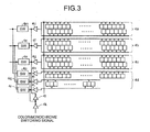
- FIG. 3 is a diagram illustrating an example of the configuration of a four-line CCD used in the embodiment.
- the four-line CCD includes three pixel groups which are a pixel group 4a for red (R), a pixel group 4b for green (G), and a pixel group 4c for blue (B).
- the four-line CCD outputs signals of three channels in total in the color mode.
- the four-line CCD further includes a pixel group 4d dedicated to monochrome (BW) reading and outputs signals of one channel, or, the pixel group 4d, when the four-line CCD performs image reading in the monochrome mode.
- BW monochrome
- Some CCDs divide a pixel group into odd pixels (ODD) and even pixels (EVEN) to output signals through two channels in the monochrome mode.
- ODD odd pixels
- EVEN even pixels
- Such a CCD can read a monochrome image at a higher speed than a three-line CCD does.
- Output signals of the red (R) pixel group 4a are amplified by an amplifier 4e.
- Output signals of the green (G) pixel group 4b are amplified by an amplifier 4f.
- Output signals of the blue (B) pixel group 4c are amplified by an amplifier 4g.
- Output signals of the monochrome (BW) pixel group 4d are amplified by amplifiers 4h, 4i, and 4j.
- the output signals of the amplifiers 4e to 4j are input to switches 4m to 4r.
- a color/monochrome switching signal is input to the switches 4p to 4r via an inverter 4k.
- the switches 4p to 4r output signals when the color/monochrome switching signal is in high level (monochrome mode).
- the color/monochrome switching signal is input to the switches 4m to 4o via the inverter 4k and an inverter 41.
- the switches 4m to 4o output signals when the color/monochrome switching signal is in low level (color
- Switching between the color reading mode and the monochrome reading mode of the four-line CCD is performed by operating switches (SWs) in the CCD according to the color/monochrome switching signal coming from the CCD-drive control unit 12 (see FIG. 1 ).
- Image signals selected from image signals transmitted from the R/G/B/BW pixel groups according to the color/monochrome switching signal are externally output from the CCD.
- a four-line CCD can include drive-clock input terminals for individually driving a shift gate and a transfer register (not shown) in a color-mode sensor (R/G/B) and a shift gate and a transfer register (not shown) in a monochrome-mode sensor (BW).
- An example of such a four-line CCD is disclosed in Japanese Patent Application Laid-open No. 2006-314039 .
- the four-line CCD used in the embodiment is of this type.
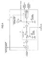
- FIG. 4 is a diagram illustrating the configuration of an output circuit (of one channel) in the CCD.
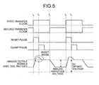
- FIG. 5 is a timing chart for input/output signals of the output circuit illustrated in FIG. 4 .
- an output circuit 21 includes a CCD transfer unit 22, a floating capacitor 23, a signal-charge draining unit 24, amplifiers 25 and 27, a clamp unit 26, and a switch (SW) 28.
- the CCD transfer unit 22 outputs signals coming from the pixels in the CCD in synchronization with first and second transfer clocks.
- the floating capacitor 23 is connected to be interposed between an output terminal of the CCD transfer unit 22 and the ground potential.
- the signal-charge draining unit 24 includes a transistor 24a.
- the transistor 24a includes a first input/output terminal connected to a junction 29 between the output terminal of the CCD transfer unit 22 and the floating capacitor 23, a second input/output terminal connected to a high-side supply voltage, and a control terminal to which a reset pulse is to be input.
- the transistor 24a While the reset pulse is in high level, in the circuit configured in this way, the transistor 24a is on state and the potential of the junction 29 is pulled up to the high-side supply voltage, thereby signal charges (electrons) are drained.
- the amplifier 25 amplifies the voltage at the junction 29 and outputs the amplified voltage.
- the clamp unit 26 includes a capacitor 26a, a DC power source 26b, and a transistor 26c.
- the capacitor 26a is connected at one end thereof to an output terminal of the amplifier 25.
- the DC power source 26b is connected at its low-side output terminal to the ground potential.
- the transistor 26c includes a first input/output terminal connected to a high-side output terminal of the DC power source 26b and a second input/output terminal connected to the other end of the capacitor 26a to serve as an output terminal of the clamp unit 26. While a clamp pulse is in high level, in the circuit configured in this way, the transistor 26c is on state , and the potential of the output terminal of the clamp unit 26 is clamped to the potential (DC offset voltage) of the DC power source 26b.
- the amplifier 27 amplifies the voltage of the output terminal of the clamp unit 26 and outputs the amplified voltage.
- the switch 28 outputs the output signal of the amplifier 27 to an external output terminal according to the color/monochrome switching signal.
- the first transfer clock is an inverted signal of the second transfer clock.
- the transistor 24a in the signal-charge draining unit 24 becomes on state, and analog output signals (OS1, OS2, and OS3) change to high level.
- the transistor 24a in the signal-charge draining unit 24 changes to off state, the transistor 26c (see FIG.
- the charges accumulated in the transfer register (not shown) in each of the sensors (R/G/B/BW) of the CCD are sequentially shifted downstream of processes in the transfer register in synchronization with the first and second transfer clocks to be converted at a last stage in the transfer register, into an analog amplitude voltage and output.
- the reset pulse causes the signal-charge draining unit 24 to drain charges accumulated at the last-stage in the transfer register.
- the reset output signal is clamped to the DC offset voltage by the clamp pulse.
- a shift pulse (not shown) is a signal to be used to transfer charges of all the pixels accumulated in a photoelectric transducer array of the CCD to the shift register in the CCD.
- One cycle of the shiffi pulse corresponds to a storage time of a light signal at each pixel.
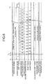
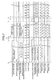
- FIG. 6 is a timing chart illustrating an example of a method for driving the four-line CCD in the monochrome reading mode.
- the four-line CCD includes a set of a color-mode shift-pulse input terminal and color-mode transfer-clock input terminals and a set of a monochrome-mode shift-pulse input terminal and monochrome-mode transfer-clock input terminals separately.
- the color/monochrome switching signal is fixed to high level, a color-mode shift pulse is fixed to low level, a color-mode first transfer clock is fixed to low level, and a color-mode second transfer clock is fixed to high level to perform the monochrome reading.
- the reset pulse changes with a predetermined pulse duty and a predetermined periodicity in a sequence of: low level ⁇ high level ⁇ low level ⁇ ⁇ .
- the clamp pulse changes with the predetermined pulse duty and the predetermined periodicity in a sequence of: low level ⁇ high level ⁇ low level ⁇ ⁇ .
- the monochrome-mode first transfer clock changes with a predetermined pulse duty and a predetermined periodicity in a sequence of: high level ⁇ low level ⁇ high level ⁇ ⁇
- the monochrome-mode second transfer clock changes with the predetermined pulse duty and the predetermined periodicity in a sequence of: low level ⁇ high level ⁇ low level ⁇ ⁇ .
- a monochrome analog output signal is output.
- the monochrome-mode shift pulse changes from low level to high level.
- a period from time t 10 to t 14 corresponds to the storage time.
- the color-mode shift pulse and the color-mode first and second transfer clocks are fixed to high level or low level as illustrated in FIG. 6 . Stopping operations of circuits that are not used in this way yields effects of reducing power consumption, reducing unwanted electromagnetic interference (EMI), and the like.
- EMI unwanted electromagnetic interference
- the color/monochrome switching signal is switched to low level (color mode); the monochrome-mode shift pulse and the monochrome-mode first and second transfer clocks are fixed to high level or low level; the color-mode shift pulse and the color-mode first and second transfer clocks are supplied as well as in the monochrome reading mode.
- the reset pulse and the clamp pulse are shared between for the color reading mode and for the monochrome reading mode, in the example illustrated in FIG. 6 .
- the CCD may include a set of a reset-pulse input terminal and a clamp-pulse input terminal for the color reading mode and that for the monochrome reading mode separately and be configured such that a reset pulse and a clamp pulse for the color reading mode and a reset pulse and a clamp pulse for the monochrome reading mode are driven individually.
- the driving method described above is disadvantageous in that an overvoltage is output at mode switching between the color reading mode and the monochrome reading mode because unnecessary charges accumulated in one sensor of the sensors that has been at rest before the mode switching are emitted at a dash immediately after the mode switching.
- the one sensor is the BW sensor when the CCD has been in the color reading mode before the mode switching, while the one sensor is the R/G/B sensor when the CCD has been in the monochrome reading mode.
- applying this overvoltage to the AFE 7 placed downstream of the CCD has an adverse effect because the amplitude value of the analog image signal falls below the lower limit of the input voltage rating of the AFE 7. This can result in degradation in characteristics or, at worst, device destruction of the AFE 7.
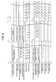
- FIG. 7 is a timing chart illustrating a comparative example of the method for driving the four-line CCD at mode switching from the monochrome reading mode to the color reading mode.
- the four-line CCD includes the set of the color-mode shift-pulse input terminal and the color-mode transfer-clock input terminals and the set of the monochrome-mode shift-pulse input terminal and the monochrome-mode transfer-clock input terminals separately.
- the color/monochrome switching signal is in high level (monochrome mode).
- the monochrome-mode shift pulse changes from low level to high level
- the clamp pulse, and the monochrome-mode first and second transfer clocks are supplied to the CCD, the analog output signal (OS1) that is directly proportional to light reflected from an original is output as described above with reference to FIG. 5 .
- the color/monochrome switching signal changes from high level (monochrome mode) to low level (color mode).
- the reset pulse changes with a predetermined pulse duty and a predetermined periodicity in a sequence of: low level ⁇ high level ⁇ low level ⁇ ⁇ .
- the reset pulse changes high level, the reset noise described above is superimposed on the analog output signals (OS1, OS2, and OS3).
- the clamp pulse changes with the predetermined pulse duty and the predetermined periodicity in a sequence of: low level ⁇ high level ⁇ low level ⁇ ⁇ .
- the analog output signals (OS1, OS2, and OS3) are clamped to the DC offset voltage as described above.
- the color-mode first transfer clock changes with a predetermined pulse duty and a predetermined periodicity in a sequence of: high level ⁇ low level ⁇ high level ⁇ ⁇
- the color-mode second transfer clock changes with the predetermined pulse duty and the predetermined periodicity in a sequence of: low level ⁇ high level ⁇ low level ⁇ ⁇ .
- charges accumulated in the R/G/B sensor that has been at rest from t 20 to t 22 are emitted, causing the amplitudes of the analog output signals (OS1, OS2, and OS3) to undesirably reach the ground potential (GND) at time t 26 , and to fall undesirably below the lower limit of the input voltage rating of the AFE 7.
- the color-mode shift pulse changes from low level to high level.
- the reset pulse changes with the predetermined pulse duty and the predetermined periodicity in a sequence of: low level ⁇ high level ⁇ low level ⁇ ⁇ .
- the reset pulse changes to high level, the reset noise described above is superimposed on the analog output signals (OS1, OS2, and OS3).
- the clamp pulse changes with the predetermined pulse duty and the predetermined periodicity in a sequence of: low level ⁇ high level ⁇ low level ⁇ ⁇ .
- the analog output signals (OS1, OS2, and OS3) are clamped to the DC offset voltage as described above.
- the color-mode first transfer clock changes with the predetermined pulse duty and the predetermined periodicity in a sequence of: high level ⁇ low level ⁇ high level ⁇ ⁇
- the color-mode second transfer clock changes with the predetermined pulse duty and the predetermined periodicity in a sequence of: low level ⁇ high level ⁇ low level ⁇ ⁇ .
- the analog output signals (OS1, OS2, and OS3) directly proportional to light reflected from an original are output.
- a driving method for a situation where the color reading mode is switched to the monochrome reading mode is similar to that described above except that the monochrome-mode drive signals and the color-mode drive signals are to be interchanged.
- FIG. 8 is a diagram illustrating the configuration of an output circuit (of one channel) in the four-line CCD according to the embodiment.
- an output circuit 31 includes an unnecessary-charge draining unit 32 in addition to constituents of the output circuit 21 described above and illustrated in FIG. 4 .
- the unnecessary-charge draining unit 32 includes an edge detection circuit 32a, a holding circuit 32b, and a transistor 32c.
- the color/monochrome switching signal is input to the edge detection circuit 32a.
- the edge detection circuit 32a outputs a high-level signal to the holding circuit 32b upon detection of an edge of the color/monochrome switching signal.
- the holding circuit 32b holds the high-level signal fed from the edge detection circuit 32a for a predetermined period of time T WAIT, and thereafter outputs the high-level signal to a control terminal of the transistor 32c.
- T WAIT The predetermined time T WAIT satisfies Expression (1) below: T WAIT > Q ALI / Q REG ⁇ T line
- Q ALL is a total of amount of charges (which is a value specific to each type of the CCD) being storable in all circuits of one channel in the CCD
- Q REG is a total amount of charges (which is a value specific to each type of the CCD) being storable in a line of the shift register in the CCD
- T line is a minimum storage time (in minutes) necessary to shift all the charges in the line of the shift register.
- the transistor 32c includes a first input/output terminal connected to a junction 29a between the amplifier 25 and the junction 29 and a second input/output terminal connected to a high-side supply voltage.
- the junction 29a is pulled up to the high-side supply voltage for a predetermined period of time after the color/monochrome switching signal changes from high level to low level or from low level to high level.
- FIG. 9 is a timing chart illustrating a method for driving the four-line CCD according to the embodiment at mode switching from the monochrome reading mode to the color reading mode.
- the four-line CCD includes the set of the color-mode shift-pulse input terminal and the color-mode transfer-clock input terminals and the set of the monochrome-mode shift-pulse input terminal and the monochrome-mode transfer-clock input terminals separately.
- the color/monochrome switching signal is in high level (monochrome mode).
- the monochrome-mode shift pulse changes from low level to high level
- the analog output signal (OS1) that is directly proportional to light reflected from an original is output as described above with reference to FIG. 5 when the reset pulse, the clamp pulse, and the monochrome-mode first and second transfer clocks are supplied to the CCD.
- the reset pulse is asserted (high level).
- the transistor 24a in the signal-charge draining unit 24 changes to on state, and the potential of the junction 29 is pulled up to the high-side supply voltage. This causes the analog output signals (OS1, OS2, and OS3) to change to high level.
- the color/monochrome switching signal changes from high level (monochrome reading mode) to low level (color reading mode).
- the clamp pulse changes with a predetermined pulse duty and a predetermined periodicity in a sequence of: low level ⁇ high level ⁇ low level ⁇ ⁇ ;
- the color-mode first transfer clock changes with a predetermined pulse duty and a predetermined periodicity in a sequence of: high level ⁇ low level ⁇ high level ⁇ ⁇ ;
- the color-mode second transfer clock changes with the predetermined pulse duty and the predetermined periodicity in a sequence of: low level ⁇ high level ⁇ low level ⁇ ⁇ .
- the analog output signals (OS1, OS2, and OS3) remain in high level because the reset pulse is kept asserted (high level).
- the analog output signals (OS1, OS2, and OS3) change to the DC offset voltage.
- the predetermined time T WAIT satisfies Expression (1) described above.
- the color-mode shift pulse changes from low level to high level, charges of the pixels in the CCD are transferred to the shift register.
- the reset pulse changes with the predetermined pulse duty and the predetermined periodicity in a sequence of: low level ⁇ high level ⁇ low level ⁇ ⁇ .
- the reset pulse changes to high level, the reset noise described above is superimposed on the analog output signals (OS1, OS2, and OS3).
- the clamp pulse changes with the predetermined pulse duty and the predetermined periodicity in a sequence of: low level ⁇ high level ⁇ low level ⁇ ⁇ .
- the analog output signals (OS1, OS2, and OS3) are clamped to the DC offset voltage as described above.
- the color-mode first transfer clock changes with the predetermined pulse duty and the predetermined periodicity in a sequence of: high level ⁇ low level ⁇ high level ⁇ ⁇
- the color-mode second transfer clock changes with the predetermined pulse duty and the predetermined periodicity in a sequence of: low level ⁇ high level ⁇ low level ⁇ ⁇ .
- the analog output signals (OS1, OS2, and OS3) directly proportional to light reflected from an original are output.
- An overvoltage that can be developed immediately after switching from the monochrome reading mode to the color reading mode can be prevented by performing resetting of the R/G/B sensor where unnecessary charges accumulated as described above at about time when the monochrome reading mode is switched to the color reading mode.
- it is unnecessary to drive the set of the color-mode shift pulse and the color-mode transfer clocks and the set of the monochrome-mode shift pulse and the monochrome-mode transfer clocks simultaneously. Accordingly, this method is also advantageous in not increasing power consumption and additional unwanted electromagnetic interference (EMI) of the drive circuits as compared with those of the driving method illustrated in FIG. 7 .
- EMI unwanted electromagnetic interference
- a driving method for a situation where the color reading mode is switched to the monochrome reading mode is similar to that described above except that the monochrome-mode drive signals illustrated in FIG. 9 are to be interchanged with the color-mode drive signals.
- the reset pulse and the clamp pulse are shared between the color reading mode and the monochrome reading mode in the example illustrated in FIG. 9 .
- the four-line CCD may include a set of a reset-pulse input terminal and a clamp-pulse input terminal for the color mode and that for the monochrome reading mode separately and be configured such that a color-mode reset pulse is kept to be asserted before switching from the monochrome reading mode to the color reading mode.
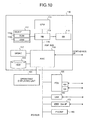
- FIG. 10 is a block diagram illustrating a hardware configuration of a multi-function peripheral (MFP) which is an example of an imaging forming apparatus that includes the image reading device according to the embodiment.
- the MFP includes a controller 110 and an engine unit (Engine) 160 that are connected to each other with a PCI (peripheral component interface) bus.
- the controller 110 is a controller that controls controlling totally the MFP, drawing, communication, and inputs from an operating unit (not shown).
- the engine unit 160 is a printer engine or the like that is connectable to the PCI bus.
- Examples of the engine unit 160 include a monochrome plotter, a one-drum color plotter, a four-drum color plotter, a scanner (corresponding to the image reading device), and a facsimile unit.
- the engine section 160 includes not only what is called as an engine unit such as the plotter, but also an image processing unit for processing an error diffusion, a gamma conversion, and the like.
- the controller 110 includes a CPU (central processing unit) 111, a north bridge (NB) 113, a system memory (hereinafter, "MEM-P") 112, a south bridge (SB) 114, a local memory (hereinafter, "MEM-C”) 117, an application-specific integrated circuit (ASIC) 116, and an HDD 118.
- An AGP (accelerated graphics port) bus 115 connects between the NB 113 and the ASIC 116.
- the MEM-P 112 further includes a ROM (Read Only Memory) 112a and a RAM (Random Access Memory) 112b.
- the CPU 111 controls the MFP totally and includes a chipset that includes the NB 113, the MEM-P 112, and the SB 114.
- the CPU 111 is connected to other devices via the chipset.
- the NB 113 is a bridge for connecting the CPU 111 to the MEM-P 112, the SB 114, and the AGP 115.
- the NB 113 includes a memory controller, a PCI master, and an AGP target.
- the memory controller controls reading and writing from and to the MEM-P 112.
- the MEM-P 112 is a system memory being a Read Only Memory that is used as a storage memory stores therein computer programs and data, an expansion memory for expanding computer programs and data, and a drawing memory for a printer, and the like, and includes the ROM 112a and the RAM 112b.
- the RAM 112b is a writable and readable memory that is used as an expansion memory for expanding computer programs and data and a drawing memory for the printer, and the like.
- the SB 114 is a bridge for connecting the NB 113 to PCI devices and peripheral devices.
- the SB 114 is connected to the NB 113 via the PCI bus, and the PCI bus to which a network interface (I/F) unit and the like are also connected.
- I/F network interface
- the ASIC 116 is an IC (Integrated Circuit) for image processing and includes a hardware component for the image processing.
- the ASIC 116 functions as a bridge that connects the AGP 115, the PCI bus, the HDD 118, and the MEM-C 117 with each other.
- the ASIC 116 includes a PCI target and an AGP master, an arbiter (ARB) which is a core of the ASIC 116, a memory controller that controls the MEM-C 117, a plurality of DMACs (direct memory access controllers ) that performs image data rotation and the like using a hardware logic or the like, and a PCI unit that transfers data between the engine section 160 and the ASIC 116 via the PCI bus.
- ARB arbiter
- DMACs direct memory access controllers
- a FCU (facsimile control unit) 130, a universal serial bus (USB) 140, and an IEEE 1394 (Institute of Electrical and Electronics Engineers 1394) 1/F 150 are connected to the ASIC 116 via the PCI bus.
- An operating/displaying unit 120 is directly connected to the ASIC 116.
- the MEM-C 117 is a local memory for use as a buffer for storing copy images and codes.
- the HDD 118 is a storage unit for accumulating image data, computer programs, font data, and forms.
- the AGP 115 is a bus interface for a graphics accelerator card introduced to speed up graphics operations and allows direct access to the MEM-P 112 with a high throughput, thereby speeding up operations related to the graphic accelerator card.
- An image reading computer program to be executed by the image reading device according to the embodiment can be provided as being preinstalled in a ROM or the like.
- the image reading computer program to be executed by the image reading device according to the embodiment can be provided as being recorded in a computer-readable recording medium such as a compact disc (CD)-ROM, a flexible disk (FD), a CD-R (CD recordable disk), or a DVD (digital versatile disk ) in an installable or executable format.
- a computer-readable recording medium such as a compact disc (CD)-ROM, a flexible disk (FD), a CD-R (CD recordable disk), or a DVD (digital versatile disk ) in an installable or executable format.
- the image reading computer program to be executed by the image reading device according to the embodiment can be stored in a computer connected to a network such as the Internet so that the computer program is provided by downloading over the network.
- the image reading computer program to be executed by the image reading device according to the embodiment can be provided or distributed via a network such as the Internet.
- the image reading computer program to be executed by the image reading device has a module structure made of the above-described units (the light-source-drive control unit, the CCD-drive control unit, the AFE-drive control unit, and the data-processing control unit).
- the CPU reads the image reading computer program from the ROM and executes it, thereby loading each of the units onto a main storage unit so that the light-source-drive control unit, the CCD-drive control unit, the AFE-drive control unit, and the data-processing control unit are generated on the main storage unit.
- the image reading device according to an aspect of the present invention is applied to an MFP that has at least two of a copier function, a facsimile function, a scanner function, and a printer function has been described.
- application is not limited thereto, and the image reading device is applicable to any image forming apparatus, such as a copier, a printer, a scanner, and a facsimile machine.
- an overvoltage that is developed at reading-mode switching between a color reading mode and a monochrome reading mode can be reduced with a simple configuration. Accordingly, effects of reducing degradation in characteristics and destruction of a circuit downstream of a photoelectric transducer are yielded.
Abstract
Description
- The present application claims priority to and incorporates by reference the entire contents of Japanese Patent Application No.
2011-165840 - The present invention relates to a photoelectric transducer that reads an image of an original or the like, and a device and a method for reading an image.
- An image reading device that reads an image of an original or the like typically includes a charge coupled device (CCD) and an analog front end (AFE) arranged downstream of the CCD. An output of the CCD is input to the AFE via alternating-current (AC)-coupling (via a capacitor connected in series therebetween). Accordingly, only an amount of change (AC) in the output of the CCD is conveyed to the AFE. Put another way, the amount of change in the output of the CCD, or, an output-fluctuation amount, is inevitably conveyed to the AFE. For instance, in a case where an overvoltage above an input voltage rating of the AFE is temporarily generated by the CCD, the overvoltage is directly conveyed to the AFE, causing degradation in characteristics of the AFE device or, at worst, device destruction to occur. Under the circumstance, such an overvoltage input to the AFE has been regarded as an important issue, and there are some known techniques for responding to the issue.
- However, the conventional techniques aim at reducing an overvoltage that is developed as a result of at-a-dash emission of unnecessary charges accumulated during power-off of a CCD immediately after power-on of the CCD. Meanwhile, a four-line CCD that generally includes a color (R/G/B) sensor as well as a monochrome (black and white (BW)) sensor has a problem that an overvoltage is developed even in a state where power is kept to be supplied to the CCD. This overvoltage is developed immediately after mode switching between a color reading mode and a monochrome reading mode as a result of at-a-dash emission of unnecessary charges accumulated in one sensor of the sensors that has been at rest before the mode switching. The one sensor the BW sensor when the CCD has been in the color reading mode before the mode switching, while the one sensor is the R/G/B sensor when the CCD has been in the monochrome reading mode.
- Meanwhile, when the technique used for switching the mode of the CCD from off state to on state is used for responding to the overvoltage that is developed at switching of the reading mode, it is required to use an additional control signal that is not a control signal for switching of the reading mode. Furthermore, this approach is also disadvantageous in requiring establishing a sequence involving these control signals, thereby making switching of the reading mode time consuming and control complicated.
- Japanese Patent Application Laid-open No.
2006-314039 - It is an object of the present invention to at least partially solve the problems in the conventional technology.
- It is an object of the present invention to reduce an overvoltage at reading-mode switching between a color reading mode and a monochrome reading mode with a simpler configuration.
- A photoelectric transducer being capable of image reading in any one of a color reading mode and a monochrome reading mode, the photoelectric transducer comprising: a color reading sensor; a monochrome reading sensor; and an unnecessary-charge draining unit that drains unnecessary charges accumulated in one of the monochrome reading sensor and the color reading sensor therefrom at switching from the color reading mode to the monochrome reading mode or the monochrome reading mode to the color reading mode.
- An image reading device comprises: a photoelectric transducer that includes a color reading sensor, a monochrome reading sensor, and a signal-charge draining unit, the photoelectric transducer being capable of image reading is any one of a color reading mode and a monochrome reading mode; and a drive control unit that controls driving of the photoelectric transducer.
- The signal-charge draining unit drains output signal charges of any one of the color reading sensor and the monochrome reading sensor therefrom while a reset pulse is asserted, the reset pulse being a pulse signal supplied from the drive control unit to the photoelectric transducer during image reading.
- The drive control unit maintains the reset pulse being asserted at switching from the color reading mode to the monochrome reading mode or from the monochrome reading mode to the color reading mode.
- An image reading method to be performed by an image reading device that includes a photoelectric transducer being capable of image reading in any one of a color reading mode and a monochrome reading mode and a drive control unit that controls driving of the photoelectric transducer, the photoelectric transducer including a color reading sensor, a monochrome reading sensor, and a signal-charge draining unit, the image reading method comprises: draining, performed by the signal-charge draining unit, output signal charges of any one of the color reading sensor and the monochrome reading sensor therefrom while a reset pulse is asserted, the reset pulse being a pulse signal supplied to the photoelectric transducer during the image reading; and maintaining, performed by the drive control unit, the reset pulse being asserted at switching from the color reading mode to the monochrome reading mode or from the monochrome reading mode to the color reading mode.
- The above and other objects, features, advantages and technical and industrial significance of this invention will be better understood by reading the following detailed description of presently preferred embodiments of the invention, when considered in connection with the accompanying drawings.
-
-
FIG. 1 is a block diagram illustrating the configuration of an image reading device according to an embodiment of the present invention; -
FIG. 2A is a diagram illustrating the configuration of an emitter follower illustrated inFIG. 1 ; -
FIG. 2B is a diagram illustrating an analog image signal in an output stage of a CCD illustrated inFIG. 1 ; -
FIG. 2C is a diagram illustrating an analog image signal in an input state of an AFE illustrated inFIG. 1 ; -
FIG. 3 is a diagram illustrating an example of the configuration of a four-line CCD used in the embodiment; -
FIG. 4 is a diagram illustrating the configuration of an output circuit (of one channel) in the CCD; -
FIG. 5 is a timing chart for input/output signals of the output circuit illustrated inFIG. 4 ; -
FIG. 6 is a timing chart illustrating an example of a method for driving the four-line CCD in a monochrome reading mode; -
FIG. 7 is a timing chart illustrating a comparative example of the method for driving the four-line CCD; -
FIG. 8 is a diagram illustrating the configuration of an output circuit (of one channel) in the four-line CCD according to the embodiment; -
FIG. 9 is a timing chart illustrating a method for driving the four-line CCD according to the embodiment; and -
FIG. 10 is a block diagram illustrating a hardware configuration of an MFP according to the embodiment. - Exemplary embodiments of the present invention are described in detail below with reference to the accompanying drawings.
FIG. 1 is a block diagram illustrating the configuration of an image reading device according to an embodiment of the present invention. Theimage reading device 1 includes alight source 2, a light-source lighting device (inverter) 3, a CCD (image sensor) 4, anemitter follower 5, anAC coupling capacitor 6, an AFE 7, adata processing unit 8, a control unit 9, and astorage unit 10. - The
light source 2 illuminates an original which is a target of image reading with light. The light-source lighting device 3 is a circuit for lighting thelight source 2. TheCCD 4 converts light reflected from the original into an electric signal (analog image signal). The configuration of theCCD 4 is described in detail later. - The
emitter follower 5 matches impedance of theCCD 4 to that of theAFE 7. TheAC coupling capacitor 6 eliminates an amount of a direct current (DC) offset voltage portion of an output voltage of theCCD 4 to make the voltage of an analog image signal output from theCCD 4 fall within an input voltage rating of theAFE 7. - The AFE (analog front end) 7 is an integrated circuit (IC) into which an analog-to-digital (A/D) conversion function, a sample and hold (S/H) circuit function, a gain adjustment function, and the like are integrated. Converting an analog image signal into a digital image signal that is to be input to the AFE 7 is one of important functions of the AFE 7. The
AFE 7 may further include a clamp function that stabilizes a voltage level of the input analog image signal to a desired fixed voltage level, an auto gain control (AGC) control function that adjusts a peak level of the converted digital image signal to a desired level, a black offset adjusting function that sets a black level to a desired level, and the like. The black level is used as a reference of image signals. - The
data processing section 8 performs various data processing such as shading correction and gamma correction on the digital image signal output from theAFE 7. The processed digital image data is either directly transmitted to awriting unit 15 or temporarily stored in thestorage unit 10 via the control unit 9 and then transmitted to thewriting unit 15 via the control unit 9. - The control unit 9 controls totally the
image reading device 1. The control unit 9 includes a light-source-drive control unit 11, a CCD-drive control unit 12, an AFE-drive control unit 13, and a data-processing control unit 14. - The light-source-
drive control unit 11 controls driving of the light-source lighting device 3 to control an amount of light emitted from thelight source 2. Specifically, the light-source-drive control unit 11 controls the amount of light emitted from thelight source 2 by inputting (applying) DC voltage or inputting a pulse-width modulation (PWM) signal to the light-source lighting device 3. - The CCD-
drive control unit 12 controls driving of theCCD 4. Specifically, the CCD-drive control unit 12 selects one of a plurality of reading modes, in which theCCD 4 is to read an original, of theCCD 4 and indicates the selected mode to theCCD 4. - The AFE-
drive control unit 13 controls driving of theAFE 7. The data-processing control unit 14 controls driving of thedata processing unit 8. Thestorage unit 10 stores various types of drive setting data and digital image data having processed by thedata processing unit 8. Thestorage unit 10 is a storage medium, e.g. a read only memory (ROM), a random access memory (RAM), or a hard disk drive (HDD). The various types of drive setting data are data that include drive setting data for thelight source 2 and the light-source lighting device 3, drive setting data for theCCD 4, drive setting data for theAFE 7, and data-processing setting data for thedata processing unit 8. - How the
image reading device 1 reads an image is briefly described below. An original is illuminated with light emitted from thelight source 2, and light reflected from the original enters into theCCD 4 via a plurality of mirrors (not shown). TheCCD 4 is driven based on the drive setting data for theCCD 4 stored in thestorage unit 10 to output an analog image signal that depends on an amount of the light entered into theCCD 4. The analog image signal is input to theAC coupling capacitor 6 via theemitter follower 5. An offset voltage of a fixed level is superimposed on the analog image signal in an output stage of theCCD 4. It is undesirable to directly input this analog image signal to theAFE 7 because the offset voltage is over the input voltage rating of theAFE 7. Hence, theAC coupling capacitor 6 is used to eliminate an amount of the offset voltage of the analog image signal so that an input-amount to theAFE 7 does not exceed the input voltage rating of theAFE 7. -
FIG. 2A is a diagram illustrating the configuration of theemitter follower 5.FIG. 2B is a diagram illustrating an analog image signal in the output state of theCCD 4.FIG. 2C is a diagram illustrating an analog image signal in an input state of theAFE 7. As illustrated inFIG. 2A , theemitter follower 5 includes aresistor 5a and atransistor 5b. Theresistor 5a is connected to the ground potential at one end. Thetransistor 5b includes a first input/output terminal connected to the other end of theresistor 5a, a second input/output terminal connected to a supply voltage (here, 10 to 12 V), and a control terminal to which an output signal of theCCD 4 is to be input. - In
FIG. 2A , for example, the supply voltage is 10 to 12 V. The analog image signal (seeFIG. 2B ) in the output stage of theCCD 4 is a 5 V offset voltage on which a analog image signal, which is a negative-going pulse, is superimposed. However, the supply voltage of theAFE 7 is 3.3 V; the input voltage rating ranges from 0 to 2 V; the offset voltage of theAFE 7 is 2 V. Therefore, it is undesirable to directly input the output signal of theCCD 4 to theAFE 7. Hence, theAC coupling capacitor 6 is used to convert the output signal of theCCD 4 into a signal (seeFIG. 2C ) which is the 2 V offset voltage with the negative-going analog image signal superimposed thereon. The converted signal is input to theAFE 7. Note that the above-mentioned voltage values are merely example values for describing the embodiment and applicable voltage values are not limited thereto. - In a case where the analog image signal in the output state of the
CCD 4 has an amplitude equal to or higher than 2 V, when the offset voltage is set to 2 V, an amplitude value of a portion of the analog image signal that is over above 2 V undesirably reaches the ground potential (GND) to fall below a lower limit of the input voltage rating of theAFE 7, and adversely affects theAFE 7, resulting in degradation in characteristics of theAFE 7 or, at worst, device destruction. Accordingly, the amplitude of the analog image signal preferably stays within the range of the input voltage rating of theAFE 7. - However, there can be a case where an overvoltage over the amplitude range is developed in a transient state, e.g. during status transition of the
CCD 4. For instance, the photoelectric transducer of theCCD 4 stores charges with responding to incident light irrespective of whether the power supply of theCCD 4 is on state or off state. This charge storage phenomenon occurs because a minute amount of ambient light is detected even when the light is not intentionally caused to enter theCCD 4. Accordingly, an overvoltage is developed at transition from power-off state to power-on state of theCCD 4 because unnecessary charges accumulated during power-off of theCCD 4 are emitted at a dash to the output terminal immediately after power-on state of theCCD 4. - Meanwhile, a four-line CCD that generally includes a color (R/G/B) sensor as well as a monochrome (BW) sensor has a problem that an overvoltage is developed even in a state where power supply to the CCD is maintained in on state. This overvoltage is developed immediately after mode switching between a color mode and a monochrome mode as a result of at-a-dash emission of unnecessary charges accumulated in one sensor of the sensors that has been at rest before the mode switching. The one sensor is the BW sensor when the CCD has been in the color mode before the mode switching, while the one sensor is the R/G/B sensor when the CCD has been in the monochrome mode.
-
FIG. 3 is a diagram illustrating an example of the configuration of a four-line CCD used in the embodiment. The four-line CCD includes three pixel groups which are apixel group 4a for red (R), apixel group 4b for green (G), and apixel group 4c for blue (B). The four-line CCD outputs signals of three channels in total in the color mode. The four-line CCD further includes apixel group 4d dedicated to monochrome (BW) reading and outputs signals of one channel, or, thepixel group 4d, when the four-line CCD performs image reading in the monochrome mode. Some CCDs divide a pixel group into odd pixels (ODD) and even pixels (EVEN) to output signals through two channels in the monochrome mode. Such a CCD can read a monochrome image at a higher speed than a three-line CCD does. - Output signals of the red (R)
pixel group 4a are amplified by anamplifier 4e. Output signals of the green (G)pixel group 4b are amplified by anamplifier 4f. Output signals of the blue (B)pixel group 4c are amplified by anamplifier 4g. Output signals of the monochrome (BW)pixel group 4d are amplified byamplifiers amplifiers 4e to 4j are input toswitches 4m to 4r. A color/monochrome switching signal is input to theswitches 4p to 4r via aninverter 4k. Theswitches 4p to 4r output signals when the color/monochrome switching signal is in high level (monochrome mode). The color/monochrome switching signal is input to theswitches 4m to 4o via theinverter 4k and aninverter 41. Theswitches 4m to 4o output signals when the color/monochrome switching signal is in low level (color mode). - Switching between the color reading mode and the monochrome reading mode of the four-line CCD is performed by operating switches (SWs) in the CCD according to the color/monochrome switching signal coming from the CCD-drive control unit 12 (see
FIG. 1 ). Image signals selected from image signals transmitted from the R/G/B/BW pixel groups according to the color/monochrome switching signal are externally output from the CCD. - A four-line CCD can include drive-clock input terminals for individually driving a shift gate and a transfer register (not shown) in a color-mode sensor (R/G/B) and a shift gate and a transfer register (not shown) in a monochrome-mode sensor (BW). An example of such a four-line CCD is disclosed in Japanese Patent Application Laid-open No.
2006-314039 - An example of a drive clock and a driving method for driving the CCD are described below with reference to
FIGS. 4 and5 .FIG. 4 is a diagram illustrating the configuration of an output circuit (of one channel) in the CCD.FIG. 5 is a timing chart for input/output signals of the output circuit illustrated inFIG. 4 . - Referring to
FIG. 4 , anoutput circuit 21 includes aCCD transfer unit 22, a floatingcapacitor 23, a signal-charge draining unit 24,amplifiers clamp unit 26, and a switch (SW) 28. - The
CCD transfer unit 22 outputs signals coming from the pixels in the CCD in synchronization with first and second transfer clocks. The floatingcapacitor 23 is connected to be interposed between an output terminal of theCCD transfer unit 22 and the ground potential. The signal-charge draining unit 24 includes atransistor 24a. Thetransistor 24a includes a first input/output terminal connected to ajunction 29 between the output terminal of theCCD transfer unit 22 and the floatingcapacitor 23, a second input/output terminal connected to a high-side supply voltage, and a control terminal to which a reset pulse is to be input. While the reset pulse is in high level, in the circuit configured in this way, thetransistor 24a is on state and the potential of thejunction 29 is pulled up to the high-side supply voltage, thereby signal charges (electrons) are drained. Theamplifier 25 amplifies the voltage at thejunction 29 and outputs the amplified voltage. - The
clamp unit 26 includes acapacitor 26a, aDC power source 26b, and atransistor 26c. Thecapacitor 26a is connected at one end thereof to an output terminal of theamplifier 25. TheDC power source 26b is connected at its low-side output terminal to the ground potential. Thetransistor 26c includes a first input/output terminal connected to a high-side output terminal of theDC power source 26b and a second input/output terminal connected to the other end of thecapacitor 26a to serve as an output terminal of theclamp unit 26. While a clamp pulse is in high level, in the circuit configured in this way, thetransistor 26c is on state , and the potential of the output terminal of theclamp unit 26 is clamped to the potential (DC offset voltage) of theDC power source 26b. Theamplifier 27 amplifies the voltage of the output terminal of theclamp unit 26 and outputs the amplified voltage. Theswitch 28 outputs the output signal of theamplifier 27 to an external output terminal according to the color/monochrome switching signal. - Referring to
FIG. 5 , the first transfer clock is an inverted signal of the second transfer clock. When the first transfer clock changes from low level to high level, the second transfer clock changes from high level to low level, and the reset pulse changes from low level to high level,, at time t0, thetransistor 24a (seeFIG. 4 ) in the signal-charge draining unit 24 becomes on state, and analog output signals (OS1, OS2, and OS3) change to high level. Thereafter, when the reset pulse changes from high level to low level and the clamp pulse changes from low level to high level, at time t1, thetransistor 24a (seeFIG. 4 ) in the signal-charge draining unit 24 changes to off state, thetransistor 26c (seeFIG. 4 ) in theclamp unit 26 changes to on state, and the analog output signals (OS1, OS2, and OS3) are clamped to the DC offset voltage. An overshoot that occurs in the analog output signals (OS1, OS2, and OS3) at about time t1 is referred to as a reset noise. - Subsequently, when the first transfer clock changes from high level to low level and the second transfer clock changes from low level to high level, at time t2, an analog amplitude voltage that is directly proportional to light reflected from an original is added to the DC offset voltage and output as the analog output signals (OS1, OS2, and OS3). Thereafter, when the first transfer clock changes from low level to high level, the second transfer clock changes from high level to low level, and the reset pulse changes from low level to high level, at time t3, the analog amplitude voltage is reset, and the reset noise is superimposed on the analog output signals (OS1, OS2, and OS3). Thereafter, when the clamp pulse changes from low level to high level, at time t4, the analog output signals (OS1, OS2, and OS3) are clamped to be stabilized at the DC offset voltage which is the reference of output signals of the CCD.
- Briefly, the charges accumulated in the transfer register (not shown) in each of the sensors (R/G/B/BW) of the CCD are sequentially shifted downstream of processes in the transfer register in synchronization with the first and second transfer clocks to be converted at a last stage in the transfer register, into an analog amplitude voltage and output. The reset pulse causes the signal-
charge draining unit 24 to drain charges accumulated at the last-stage in the transfer register. The reset output signal is clamped to the DC offset voltage by the clamp pulse. A shift pulse (not shown) is a signal to be used to transfer charges of all the pixels accumulated in a photoelectric transducer array of the CCD to the shift register in the CCD. One cycle of the shiffi pulse corresponds to a storage time of a light signal at each pixel. -
FIG. 6 is a timing chart illustrating an example of a method for driving the four-line CCD in the monochrome reading mode. The four-line CCD includes a set of a color-mode shift-pulse input terminal and color-mode transfer-clock input terminals and a set of a monochrome-mode shift-pulse input terminal and monochrome-mode transfer-clock input terminals separately. - The color/monochrome switching signal is fixed to high level, a color-mode shift pulse is fixed to low level, a color-mode first transfer clock is fixed to low level, and a color-mode second transfer clock is fixed to high level to perform the monochrome reading.
- When the monochrome-mode shift pulse changes from low level to high level, at time t10, charges of the pixels in the CCD are transferred to the shift register. From time t11, the reset pulse changes with a predetermined pulse duty and a predetermined periodicity in a sequence of: low level → high level → low level → ···. From time t12, the clamp pulse changes with the predetermined pulse duty and the predetermined periodicity in a sequence of: low level → high level → low level → ···. From time t13, the monochrome-mode first transfer clock changes with a predetermined pulse duty and a predetermined periodicity in a sequence of: high level → low level → high level → ··· , while the monochrome-mode second transfer clock changes with the predetermined pulse duty and the predetermined periodicity in a sequence of: low level → high level → low level → ···. As a result, a monochrome analog output signal is output. At time t14, the monochrome-mode shift pulse changes from low level to high level. A period from time t10 to t14 corresponds to the storage time.
- It is unnecessary to drive the color-mode sensor in the monochrome reading mode. Accordingly, the color-mode shift pulse and the color-mode first and second transfer clocks are fixed to high level or low level as illustrated in
FIG. 6 . Stopping operations of circuits that are not used in this way yields effects of reducing power consumption, reducing unwanted electromagnetic interference (EMI), and the like. - Although not shown, in the color reading mode, the color/monochrome switching signal is switched to low level (color mode); the monochrome-mode shift pulse and the monochrome-mode first and second transfer clocks are fixed to high level or low level; the color-mode shift pulse and the color-mode first and second transfer clocks are supplied as well as in the monochrome reading mode.
- The reset pulse and the clamp pulse are shared between for the color reading mode and for the monochrome reading mode, in the example illustrated in
FIG. 6 . Alternatively, the CCD may include a set of a reset-pulse input terminal and a clamp-pulse input terminal for the color reading mode and that for the monochrome reading mode separately and be configured such that a reset pulse and a clamp pulse for the color reading mode and a reset pulse and a clamp pulse for the monochrome reading mode are driven individually. - Meanwhile, light strikes all the sensors in the four-line CCD, causing accumulation of charges. Accordingly, the driving method described above is disadvantageous in that an overvoltage is output at mode switching between the color reading mode and the monochrome reading mode because unnecessary charges accumulated in one sensor of the sensors that has been at rest before the mode switching are emitted at a dash immediately after the mode switching. The one sensor is the BW sensor when the CCD has been in the color reading mode before the mode switching, while the one sensor is the R/G/B sensor when the CCD has been in the monochrome reading mode. As having been described above, applying this overvoltage to the
AFE 7 placed downstream of the CCD has an adverse effect because the amplitude value of the analog image signal falls below the lower limit of the input voltage rating of theAFE 7. This can result in degradation in characteristics or, at worst, device destruction of theAFE 7. -
FIG. 7 is a timing chart illustrating a comparative example of the method for driving the four-line CCD at mode switching from the monochrome reading mode to the color reading mode. The four-line CCD includes the set of the color-mode shift-pulse input terminal and the color-mode transfer-clock input terminals and the set of the monochrome-mode shift-pulse input terminal and the monochrome-mode transfer-clock input terminals separately. - At initial time t20, the color/monochrome switching signal is in high level (monochrome mode). When the monochrome-mode shift pulse changes from low level to high level, at time t21, charges of the pixels in the CCD are transferred to the shift register. Thereafter, when the reset pulse, the clamp pulse, and the monochrome-mode first and second transfer clocks are supplied to the CCD, the analog output signal (OS1) that is directly proportional to light reflected from an original is output as described above with reference to
FIG. 5 . - At time t22, the color/monochrome switching signal changes from high level (monochrome mode) to low level (color mode). From time t23, the reset pulse changes with a predetermined pulse duty and a predetermined periodicity in a sequence of: low level → high level → low level → ···. When the reset pulse changes high level, the reset noise described above is superimposed on the analog output signals (OS1, OS2, and OS3). From time t24, the clamp pulse changes with the predetermined pulse duty and the predetermined periodicity in a sequence of: low level → high level → low level → ···. When the clamp pulse changes to high level, the analog output signals (OS1, OS2, and OS3) are clamped to the DC offset voltage as described above. From time t25, the color-mode first transfer clock changes with a predetermined pulse duty and a predetermined periodicity in a sequence of: high level → low level → high level → ··· , while the color-mode second transfer clock changes with the predetermined pulse duty and the predetermined periodicity in a sequence of: low level → high level → low level → ···. Then, charges accumulated in the R/G/B sensor that has been at rest from t20 to t22 are emitted, causing the amplitudes of the analog output signals (OS1, OS2, and OS3) to undesirably reach the ground potential (GND) at time t26, and to fall undesirably below the lower limit of the input voltage rating of the
AFE 7. - Thereafter, when a predetermined period of time has elapsed, emission of the charges accumulated in the R/G/B sensor is completed. At time t27, the color-mode shift pulse changes from low level to high level. From time t28, the reset pulse changes with the predetermined pulse duty and the predetermined periodicity in a sequence of: low level → high level → low level → ···. When the reset pulse changes to high level, the reset noise described above is superimposed on the analog output signals (OS1, OS2, and OS3). From time t29, the clamp pulse changes with the predetermined pulse duty and the predetermined periodicity in a sequence of: low level → high level → low level → ···. When the clamp pulse changes to high level, the analog output signals (OS1, OS2, and OS3) are clamped to the DC offset voltage as described above. From time t30, the color-mode first transfer clock changes with the predetermined pulse duty and the predetermined periodicity in a sequence of: high level → low level → high level → ··· , while the color-mode second transfer clock changes with the predetermined pulse duty and the predetermined periodicity in a sequence of: low level → high level → low level → ···. Then, the analog output signals (OS1, OS2, and OS3) directly proportional to light reflected from an original are output.
- The example in which the monochrome reading mode is switched to the color reading mode has been described with reference to
FIG. 7 . A driving method for a situation where the color reading mode is switched to the monochrome reading mode is similar to that described above except that the monochrome-mode drive signals and the color-mode drive signals are to be interchanged. -
FIG. 8 is a diagram illustrating the configuration of an output circuit (of one channel) in the four-line CCD according to the embodiment. Referring toFIG. 8 , anoutput circuit 31 includes an unnecessary-charge draining unit 32 in addition to constituents of theoutput circuit 21 described above and illustrated inFIG. 4 . The unnecessary-charge draining unit 32 includes anedge detection circuit 32a, a holdingcircuit 32b, and atransistor 32c. - The color/monochrome switching signal is input to the
edge detection circuit 32a. Theedge detection circuit 32a outputs a high-level signal to the holdingcircuit 32b upon detection of an edge of the color/monochrome switching signal. The holdingcircuit 32b holds the high-level signal fed from theedge detection circuit 32a for a predetermined period of time TWAIT, and thereafter outputs the high-level signal to a control terminal of thetransistor 32c. The predetermined time TWAIT satisfies Expression (1) below:
where QALL is a total of amount of charges (which is a value specific to each type of the CCD) being storable in all circuits of one channel in the CCD, QREG is a total amount of charges (which is a value specific to each type of the CCD) being storable in a line of the shift register in the CCD, and Tline is a minimum storage time (in minutes) necessary to shift all the charges in the line of the shift register. - The
transistor 32c includes a first input/output terminal connected to ajunction 29a between theamplifier 25 and thejunction 29 and a second input/output terminal connected to a high-side supply voltage. In the circuit configured as described above, thejunction 29a is pulled up to the high-side supply voltage for a predetermined period of time after the color/monochrome switching signal changes from high level to low level or from low level to high level. - This prevents such an undesirable situation that the amplitudes of the analog output signals (OS1, OS2, and OS3) reach the ground potential (GND) as in the case from time t26 to time t27 of the example illustrated in
FIG. 7 . Accordingly, degradation in characteristics or, at worst, device destruction in theAFE 7 placed downstream of theCCD 4 is prevented. -
FIG. 9 is a timing chart illustrating a method for driving the four-line CCD according to the embodiment at mode switching from the monochrome reading mode to the color reading mode. The four-line CCD includes the set of the color-mode shift-pulse input terminal and the color-mode transfer-clock input terminals and the set of the monochrome-mode shift-pulse input terminal and the monochrome-mode transfer-clock input terminals separately. - At initial time t40, the color/monochrome switching signal is in high level (monochrome mode). When the monochrome-mode shift pulse changes from low level to high level, at time t41, charges of the pixels in the CCD are transferred to the shift register. Thereafter, the analog output signal (OS1) that is directly proportional to light reflected from an original is output as described above with reference to
FIG. 5 when the reset pulse, the clamp pulse, and the monochrome-mode first and second transfer clocks are supplied to the CCD. - At time t42, the reset pulse is asserted (high level). In response thereto, the
transistor 24a (seeFIG. 4 ) in the signal-charge draining unit 24 changes to on state, and the potential of thejunction 29 is pulled up to the high-side supply voltage. This causes the analog output signals (OS1, OS2, and OS3) to change to high level. - At time t43, the color/monochrome switching signal changes from high level (monochrome reading mode) to low level (color reading mode). Thereafter, the clamp pulse changes with a predetermined pulse duty and a predetermined periodicity in a sequence of: low level → high level → low level → ··· ; the color-mode first transfer clock changes with a predetermined pulse duty and a predetermined periodicity in a sequence of: high level → low level → high level → ··· ; the color-mode second transfer clock changes with the predetermined pulse duty and the predetermined periodicity in a sequence of: low level → high level → low level → ···. Note that the analog output signals (OS1, OS2, and OS3) remain in high level because the reset pulse is kept asserted (high level).
- When the reset pulse is negated (low) at time t44 after a lapse of the predetermined time TWAIT from time t43, the analog output signals (OS1, OS2, and OS3) change to the DC offset voltage. The predetermined time TWAIT satisfies Expression (1) described above. When the color-mode shift pulse changes from low level to high level, charges of the pixels in the CCD are transferred to the shift register. From time t45, the reset pulse changes with the predetermined pulse duty and the predetermined periodicity in a sequence of: low level → high level → low level → ···. When the reset pulse changes to high level, the reset noise described above is superimposed on the analog output signals (OS1, OS2, and OS3). From time t46, the clamp pulse changes with the predetermined pulse duty and the predetermined periodicity in a sequence of: low level → high level → low level → ···. When the clamp pulse changes to high level, the analog output signals (OS1, OS2, and OS3) are clamped to the DC offset voltage as described above. From time t47, the color-mode first transfer clock changes with the predetermined pulse duty and the predetermined periodicity in a sequence of: high level → low level → high level → ··· , while the color-mode second transfer clock changes with the predetermined pulse duty and the predetermined periodicity in a sequence of: low level → high level → low level → ···. Then, the analog output signals (OS1, OS2, and OS3) directly proportional to light reflected from an original are output.
- An overvoltage that can be developed immediately after switching from the monochrome reading mode to the color reading mode can be prevented by performing resetting of the R/G/B sensor where unnecessary charges accumulated as described above at about time when the monochrome reading mode is switched to the color reading mode. This leads to prevention of degradation in characteristics or, at worst, device destruction in the
AFE 7 placed downstream of the CCD. Furthermore, it is unnecessary to drive the set of the color-mode shift pulse and the color-mode transfer clocks and the set of the monochrome-mode shift pulse and the monochrome-mode transfer clocks simultaneously. Accordingly, this method is also advantageous in not increasing power consumption and additional unwanted electromagnetic interference (EMI) of the drive circuits as compared with those of the driving method illustrated inFIG. 7 . - Meanwhile, a driving method for a situation where the color reading mode is switched to the monochrome reading mode is similar to that described above except that the monochrome-mode drive signals illustrated in
FIG. 9 are to be interchanged with the color-mode drive signals. The reset pulse and the clamp pulse are shared between the color reading mode and the monochrome reading mode in the example illustrated inFIG. 9 . Alternatively, the four-line CCD may include a set of a reset-pulse input terminal and a clamp-pulse input terminal for the color mode and that for the monochrome reading mode separately and be configured such that a color-mode reset pulse is kept to be asserted before switching from the monochrome reading mode to the color reading mode. -
FIG. 10 is a block diagram illustrating a hardware configuration of a multi-function peripheral (MFP) which is an example of an imaging forming apparatus that includes the image reading device according to the embodiment. As illustrated inFIG. 10 , the MFP includes acontroller 110 and an engine unit (Engine) 160 that are connected to each other with a PCI (peripheral component interface) bus. Thecontroller 110 is a controller that controls controlling totally the MFP, drawing, communication, and inputs from an operating unit (not shown). Theengine unit 160 is a printer engine or the like that is connectable to the PCI bus. Examples of theengine unit 160 include a monochrome plotter, a one-drum color plotter, a four-drum color plotter, a scanner (corresponding to the image reading device), and a facsimile unit. Note that theengine section 160 includes not only what is called as an engine unit such as the plotter, but also an image processing unit for processing an error diffusion, a gamma conversion, and the like. - The
controller 110 includes a CPU (central processing unit) 111, a north bridge (NB) 113, a system memory (hereinafter, "MEM-P") 112, a south bridge (SB) 114, a local memory (hereinafter, "MEM-C") 117, an application-specific integrated circuit (ASIC) 116, and anHDD 118. An AGP (accelerated graphics port)bus 115 connects between theNB 113 and theASIC 116. The MEM-P 112 further includes a ROM (Read Only Memory) 112a and a RAM (Random Access Memory) 112b. - The
CPU 111 controls the MFP totally and includes a chipset that includes theNB 113, the MEM-P 112, and theSB 114. TheCPU 111 is connected to other devices via the chipset. - The
NB 113 is a bridge for connecting theCPU 111 to the MEM-P 112, theSB 114, and theAGP 115. TheNB 113 includes a memory controller, a PCI master, and an AGP target. The memory controller controls reading and writing from and to the MEM-P 112. - The MEM-
P 112 is a system memory being a Read Only Memory that is used as a storage memory stores therein computer programs and data, an expansion memory for expanding computer programs and data, and a drawing memory for a printer, and the like, and includes theROM 112a and theRAM 112b. TheRAM 112b is a writable and readable memory that is used as an expansion memory for expanding computer programs and data and a drawing memory for the printer, and the like. - The
SB 114 is a bridge for connecting theNB 113 to PCI devices and peripheral devices. TheSB 114 is connected to theNB 113 via the PCI bus, and the PCI bus to which a network interface (I/F) unit and the like are also connected. - The
ASIC 116 is an IC (Integrated Circuit) for image processing and includes a hardware component for the image processing. TheASIC 116 functions as a bridge that connects theAGP 115, the PCI bus, theHDD 118, and the MEM-C 117 with each other. TheASIC 116 includes a PCI target and an AGP master, an arbiter (ARB) which is a core of theASIC 116, a memory controller that controls the MEM-C 117, a plurality of DMACs (direct memory access controllers ) that performs image data rotation and the like using a hardware logic or the like, and a PCI unit that transfers data between theengine section 160 and theASIC 116 via the PCI bus. A FCU (facsimile control unit) 130, a universal serial bus (USB) 140, and an IEEE 1394 (Institute of Electrical and Electronics Engineers 1394) 1/F 150 are connected to theASIC 116 via the PCI bus. An operating/displayingunit 120 is directly connected to theASIC 116. - The MEM-
C 117 is a local memory for use as a buffer for storing copy images and codes. TheHDD 118 is a storage unit for accumulating image data, computer programs, font data, and forms. - The
AGP 115 is a bus interface for a graphics accelerator card introduced to speed up graphics operations and allows direct access to the MEM-P 112 with a high throughput, thereby speeding up operations related to the graphic accelerator card. - An image reading computer program to be executed by the image reading device according to the embodiment can be provided as being preinstalled in a ROM or the like. The image reading computer program to be executed by the image reading device according to the embodiment can be provided as being recorded in a computer-readable recording medium such as a compact disc (CD)-ROM, a flexible disk (FD), a CD-R (CD recordable disk), or a DVD (digital versatile disk ) in an installable or executable format.
- The image reading computer program to be executed by the image reading device according to the embodiment can be stored in a computer connected to a network such as the Internet so that the computer program is provided by downloading over the network. The image reading computer program to be executed by the image reading device according to the embodiment can be provided or distributed via a network such as the Internet.
- The image reading computer program to be executed by the image reading device according to the embodiment has a module structure made of the above-described units (the light-source-drive control unit, the CCD-drive control unit, the AFE-drive control unit, and the data-processing control unit). From a viewpoint of actual hardware, the CPU (processor) reads the image reading computer program from the ROM and executes it, thereby loading each of the units onto a main storage unit so that the light-source-drive control unit, the CCD-drive control unit, the AFE-drive control unit, and the data-processing control unit are generated on the main storage unit.
- In the embodiment, an example in which the image reading device according to an aspect of the present invention is applied to an MFP that has at least two of a copier function, a facsimile function, a scanner function, and a printer function has been described. However, application is not limited thereto, and the image reading device is applicable to any image forming apparatus, such as a copier, a printer, a scanner, and a facsimile machine.
- According to an aspect of the present invention, an overvoltage that is developed at reading-mode switching between a color reading mode and a monochrome reading mode can be reduced with a simple configuration. Accordingly, effects of reducing degradation in characteristics and destruction of a circuit downstream of a photoelectric transducer are yielded.
- Although the invention has been described with respect to specific embodiments for a complete and clear disclosure, the appended claims are not to be thus limited but are to be construed as embodying all modifications and alternative constructions that may occur to one skilled in the art that fairly fall within the basic teaching herein set forth.
Claims (7)
- A photoelectric transducer (4) being capable of image reading in any one of a color reading mode and a monochrome reading mode, the photoelectric transducer (4) comprising:a color reading sensor;a monochrome reading sensor; andan unnecessary-charge draining unit (32) that drains unnecessary charges accumulated in one of the monochrome reading sensor and the color reading sensor therefrom at switching from the color reading mode to the monochrome reading mode or from the monochrome reading mode to the color reading mode.
- An image reading device (1) comprising:a photoelectric transducer (4) that includes a color reading sensor, a monochrome reading sensor, and a signal-charge draining unit (24), the photoelectric transducer (4) being capable of image reading is any one of a color reading mode and a monochrome reading mode; anda drive control unit (12) that controls driving of the photoelectric transducer (4), whereinthe signal-charge draining unit (24) drains output signal charges of any one of the color reading sensor and the monochrome reading sensor therefrom while a reset pulse is asserted, the reset pulse being a pulse signal supplied from the drive control unit (12) to the photoelectric transducer (4) during image reading, andthe drive control unit (12) maintains the reset pulse being asserted at switching from the color reading mode to the monochrome reading mode or from the monochrome reading mode to the color reading mode.
- The image reading device (1) according to claim 2, wherein
the drive control unit (12) asserts the reset pulse before the drive control unit (12) performs the switching from the color reading mode to the monochrome reading mode or from the monochrome reading mode to the color reading mode, and
the drive control unit (12) negates the reset pulse when a predetermined period of time has elapsed since the switching. - The image reading device (1) according to claim 3, wherein the predetermined period of time satisfies a following condition:

where TWAIT is the predetermined period of time in minutes, QALL is a total amount of charges being storable in all circuits of one channel including a plurality of pixels that receive light of a predetermined color in the photoelectric transducer (4), QREG is a total amount of charges being storable in a line of a shift register in the photoelectric transducer (4), and Tline is a minimum storage time in minutes being necessary to transfer all the charges in the line of the shift register. - An image reading method to be performed by an image reading device (1) that includes a photoelectric transducer (4) being capable of image reading in any one of a color reading mode and a monochrome reading mode and a drive control unit (12) that controls driving of the photoelectric transducer (4), the photoelectric transducer (4) including a color reading sensor, a monochrome reading sensor, and a signal-charge draining unit (24), the image reading method comprising:draining, performed by the signal-charge draining unit (24), output signal charges of any one of the color reading sensor and the monochrome reading sensor therefrom while a reset pulse is asserted, the reset pulse being a pulse signal supplied to the photoelectric transducer (4) during the image reading; andmaintaining, performed by the drive control unit (12), the reset pulse being asserted at switching from the color reading mode to the monochrome reading mode or from the monochrome reading mode to the color reading mode.
- The image reading method according to claim 5, wherein
asserting, performed by the drive control unit (12), the reset pulse before the drive control unit (12) performs the switching from the color reading mode to the monochrome reading mode or from the monochrome reading mode to the color reading mode, and
negating, performed by the drive control unit (12), the reset pulse when a predetermined period of time has elapsed since the switching. - The image reading method according to claim 6, wherein the predetermined period of time satisfies a following condition:

where TWAIT is the predetermined period of time in minutes, QALL is a total amount of charges being storable in all circuits of one channel including a plurality of pixels that receive light of a predetermined color in the photoelectric transducer (4), QREG is a total amount of charges being storable in a line of a shift register in the photoelectric transducer (4), and Tline is a minimum storage time in minutes being necessary to transfer all the charges in the line of the shift register.
Applications Claiming Priority (1)
| Application Number | Priority Date | Filing Date | Title |
|---|---|---|---|
| JP2011165840A JP5909909B2 (en) | 2011-07-28 | 2011-07-28 | Image reading apparatus, image forming apparatus, image reading method, and image reading program |
Publications (3)
| Publication Number | Publication Date |
|---|---|
| EP2552117A2 true EP2552117A2 (en) | 2013-01-30 |
| EP2552117A3 EP2552117A3 (en) | 2013-10-09 |
| EP2552117B1 EP2552117B1 (en) | 2020-09-02 |
Family
ID=46980719
Family Applications (1)
| Application Number | Title | Priority Date | Filing Date |
|---|---|---|---|
| EP12176075.5A Active EP2552117B1 (en) | 2011-07-28 | 2012-07-12 | Photoelectric transducer, image reading device, and image reading method |
Country Status (4)
| Country | Link |
|---|---|
| US (1) | US8937273B2 (en) |
| EP (1) | EP2552117B1 (en) |
| JP (1) | JP5909909B2 (en) |
| CN (1) | CN102905048B (en) |
Cited By (1)
| Publication number | Priority date | Publication date | Assignee | Title |
|---|---|---|---|---|
| US20220303507A1 (en) * | 2021-03-18 | 2022-09-22 | Kabushiki Kaisha Toshiba | Solid-state imaging device |
Families Citing this family (3)
| Publication number | Priority date | Publication date | Assignee | Title |
|---|---|---|---|---|
| JP2013225845A (en) | 2012-03-21 | 2013-10-31 | Ricoh Co Ltd | Imaging device, image reading device, image forming apparatus, and image reading method |
| JP6451104B2 (en) | 2014-07-04 | 2019-01-16 | 株式会社リコー | Photoelectric conversion element, image reading apparatus, image forming apparatus, and signal control method |
| CN112584744A (en) * | 2018-08-28 | 2021-03-30 | 奥林巴斯株式会社 | Endoscope, driving method, and program |
Citations (1)
| Publication number | Priority date | Publication date | Assignee | Title |
|---|---|---|---|---|
| JP2006314039A (en) | 2005-05-09 | 2006-11-16 | Ricoh Co Ltd | Image processing apparatus, image reading apparatus, image forming apparatus, computer program, and recording medium |
Family Cites Families (9)
| Publication number | Priority date | Publication date | Assignee | Title |
|---|---|---|---|---|
| JP3262441B2 (en) | 1994-02-04 | 2002-03-04 | キヤノン株式会社 | Linear image sensor and image reading device |
| JP3555416B2 (en) * | 1996-12-13 | 2004-08-18 | 富士ゼロックス株式会社 | Image reading apparatus and image reading method |
| JP3893424B2 (en) * | 1998-11-06 | 2007-03-14 | 富士フイルム株式会社 | Solid-state imaging device and signal readout method |
| US7339709B2 (en) * | 2003-03-04 | 2008-03-04 | Kabushiki Kaisha Toshiba | Method and apparatus for forming image |
| JP2005197922A (en) * | 2004-01-06 | 2005-07-21 | Fuji Xerox Co Ltd | Image reading apparatus |
| JP4692196B2 (en) | 2005-10-04 | 2011-06-01 | ソニー株式会社 | Solid-state imaging device, driving method of solid-state imaging device, and imaging device |
| JP4620025B2 (en) | 2005-11-29 | 2011-01-26 | 株式会社リコー | Image reading apparatus, information processing apparatus, and program |
| US7855742B2 (en) | 2006-03-30 | 2010-12-21 | Fujifilm Corporation | Solid state imaging device with horizontal transfer paths and a driving method therefor |
| JP4474656B2 (en) * | 2007-09-14 | 2010-06-09 | 富士ゼロックス株式会社 | Image reading apparatus, image forming apparatus, and program |
-
2011
- 2011-07-28 JP JP2011165840A patent/JP5909909B2/en not_active Expired - Fee Related
-
2012
- 2012-07-12 US US13/547,806 patent/US8937273B2/en not_active Expired - Fee Related
- 2012-07-12 EP EP12176075.5A patent/EP2552117B1/en active Active
- 2012-07-26 CN CN201210380116.3A patent/CN102905048B/en not_active Expired - Fee Related
Patent Citations (1)
| Publication number | Priority date | Publication date | Assignee | Title |
|---|---|---|---|---|
| JP2006314039A (en) | 2005-05-09 | 2006-11-16 | Ricoh Co Ltd | Image processing apparatus, image reading apparatus, image forming apparatus, computer program, and recording medium |
Cited By (2)
| Publication number | Priority date | Publication date | Assignee | Title |
|---|---|---|---|---|
| US20220303507A1 (en) * | 2021-03-18 | 2022-09-22 | Kabushiki Kaisha Toshiba | Solid-state imaging device |
| US11736817B2 (en) * | 2021-03-18 | 2023-08-22 | Kabushiki Kaisha Toshiba | Solid-state imaging device |
Also Published As
| Publication number | Publication date |
|---|---|
| US20130026348A1 (en) | 2013-01-31 |
| EP2552117B1 (en) | 2020-09-02 |
| US8937273B2 (en) | 2015-01-20 |
| CN102905048B (en) | 2015-11-25 |
| JP5909909B2 (en) | 2016-04-27 |
| JP2013030999A (en) | 2013-02-07 |
| CN102905048A (en) | 2013-01-30 |
| EP2552117A3 (en) | 2013-10-09 |
Similar Documents
| Publication | Publication Date | Title |
|---|---|---|
| US10475844B2 (en) | Photoelectric conversion device, photoelectric conversion method, and image forming apparatus | |
| US9628654B2 (en) | Processing device, image reading device, image forming apparatus, and processing method | |
| US8212908B2 (en) | Timing generator and image scanning apparatus | |
| KR20160070753A (en) | Analogue digital conversion with ramp, with multiple conversions or a single conversion depending on the light level received by a pixel | |
| US8937273B2 (en) | Photoelectric transducer, image reading device having a control unit with a reset pulse switching from a color reading mode to a monochrome reading mode | |
| US10225496B2 (en) | Photoelectric conversion device having a holding circuit with a plurality of holding units provided for each of a plurality of columns of pixels and method of driving photoelectric conversion device | |
| EP0920193A2 (en) | Image processing apparatus and method | |
| US8947753B2 (en) | Imaging device for an image reading apparatus, and image reading method | |
| JP4675698B2 (en) | Image reading device | |
| JP4059500B2 (en) | Image reading device | |
| JP4192111B2 (en) | Image input device | |
| JP4361476B2 (en) | Image reading apparatus and image forming apparatus | |
| US8849067B2 (en) | Image processing apparatus, computer-readable storage medium, and image processing method for improving image data transfer | |
| JP2010103911A (en) | Image reader | |
| KR100248226B1 (en) | Method and apparatus of brightness control for image scanner | |
| US11039035B2 (en) | Signal processing circuit, image reading apparatus, and image forming apparatus | |
| KR100240069B1 (en) | Image processing method | |
| JP2000307852A (en) | Image reader | |
| JP2003244453A (en) | Image reader | |
| KR100271155B1 (en) | Drive signal generation circuit of a photoelectric conversion sensor | |
| JP5830889B2 (en) | Image processing apparatus, program, and adjustment method | |
| JP2010028817A (en) | Image reader, image forming apparatus, and image reading method | |
| JP2012191578A (en) | Driving method of 4 line ccd unit, image reading method, image reader and image forming device | |
| JP2002271570A (en) | Image reader | |
| KR19990038528A (en) | Preprocessor of image input device and image distortion correction method using same |
Legal Events
| Date | Code | Title | Description |
|---|---|---|---|
| PUAI | Public reference made under article 153(3) epc to a published international application that has entered the european phase |
Free format text: ORIGINAL CODE: 0009012 |
|
| 17P | Request for examination filed |
Effective date: 20120712 |
|
| AK | Designated contracting states |
Kind code of ref document: A2 Designated state(s): AL AT BE BG CH CY CZ DE DK EE ES FI FR GB GR HR HU IE IS IT LI LT LU LV MC MK MT NL NO PL PT RO RS SE SI SK SM TR |
|
| AX | Request for extension of the european patent |
Extension state: BA ME |
|
| PUAL | Search report despatched |
Free format text: ORIGINAL CODE: 0009013 |
|
| AK | Designated contracting states |
Kind code of ref document: A3 Designated state(s): AL AT BE BG CH CY CZ DE DK EE ES FI FR GB GR HR HU IE IS IT LI LT LU LV MC MK MT NL NO PL PT RO RS SE SI SK SM TR |
|
| AX | Request for extension of the european patent |
Extension state: BA ME |
|
| RIC1 | Information provided on ipc code assigned before grant |
Ipc: H04N 9/04 20060101AFI20130903BHEP |
|
| STAA | Information on the status of an ep patent application or granted ep patent |
Free format text: STATUS: EXAMINATION IS IN PROGRESS |
|
| 17Q | First examination report despatched |
Effective date: 20161103 |
|
| REG | Reference to a national code |
Ref country code: DE Ref legal event code: R079 Ref document number: 602012072064 Country of ref document: DE Free format text: PREVIOUS MAIN CLASS: H04N0009040000 Ipc: H04N0005232000 |
|
| GRAP | Despatch of communication of intention to grant a patent |
Free format text: ORIGINAL CODE: EPIDOSNIGR1 |
|
| STAA | Information on the status of an ep patent application or granted ep patent |
Free format text: STATUS: GRANT OF PATENT IS INTENDED |
|
| RIC1 | Information provided on ipc code assigned before grant |
Ipc: H04N 1/03 20060101ALI20200117BHEP Ipc: H04N 5/369 20110101ALI20200117BHEP Ipc: H04N 5/232 20060101AFI20200117BHEP Ipc: H04N 1/193 20060101ALI20200117BHEP Ipc: H04N 9/04 20060101ALI20200117BHEP Ipc: H04N 5/378 20110101ALI20200117BHEP Ipc: H04N 5/359 20110101ALI20200117BHEP |
|
| INTG | Intention to grant announced |
Effective date: 20200219 |
|
| GRAS | Grant fee paid |
Free format text: ORIGINAL CODE: EPIDOSNIGR3 |
|
| GRAA | (expected) grant |
Free format text: ORIGINAL CODE: 0009210 |
|
| STAA | Information on the status of an ep patent application or granted ep patent |
Free format text: STATUS: THE PATENT HAS BEEN GRANTED |
|
| AK | Designated contracting states |
Kind code of ref document: B1 Designated state(s): AL AT BE BG CH CY CZ DE DK EE ES FI FR GB GR HR HU IE IS IT LI LT LU LV MC MK MT NL NO PL PT RO RS SE SI SK SM TR |
|
| REG | Reference to a national code |
Ref country code: GB Ref legal event code: FG4D |
|
| REG | Reference to a national code |
Ref country code: AT Ref legal event code: REF Ref document number: 1310161 Country of ref document: AT Kind code of ref document: T Effective date: 20200915 Ref country code: CH Ref legal event code: EP |
|
| REG | Reference to a national code |
Ref country code: DE Ref legal event code: R096 Ref document number: 602012072064 Country of ref document: DE |
|
| REG | Reference to a national code |
Ref country code: IE Ref legal event code: FG4D |
|
| REG | Reference to a national code |
Ref country code: NL Ref legal event code: FP |
|
| REG | Reference to a national code |
Ref country code: LT Ref legal event code: MG4D |
|
| PG25 | Lapsed in a contracting state [announced via postgrant information from national office to epo] |
Ref country code: SE Free format text: LAPSE BECAUSE OF FAILURE TO SUBMIT A TRANSLATION OF THE DESCRIPTION OR TO PAY THE FEE WITHIN THE PRESCRIBED TIME-LIMIT Effective date: 20200902 Ref country code: NO Free format text: LAPSE BECAUSE OF FAILURE TO SUBMIT A TRANSLATION OF THE DESCRIPTION OR TO PAY THE FEE WITHIN THE PRESCRIBED TIME-LIMIT Effective date: 20201202 Ref country code: BG Free format text: LAPSE BECAUSE OF FAILURE TO SUBMIT A TRANSLATION OF THE DESCRIPTION OR TO PAY THE FEE WITHIN THE PRESCRIBED TIME-LIMIT Effective date: 20201202 Ref country code: GR Free format text: LAPSE BECAUSE OF FAILURE TO SUBMIT A TRANSLATION OF THE DESCRIPTION OR TO PAY THE FEE WITHIN THE PRESCRIBED TIME-LIMIT Effective date: 20201203 Ref country code: FI Free format text: LAPSE BECAUSE OF FAILURE TO SUBMIT A TRANSLATION OF THE DESCRIPTION OR TO PAY THE FEE WITHIN THE PRESCRIBED TIME-LIMIT Effective date: 20200902 Ref country code: LT Free format text: LAPSE BECAUSE OF FAILURE TO SUBMIT A TRANSLATION OF THE DESCRIPTION OR TO PAY THE FEE WITHIN THE PRESCRIBED TIME-LIMIT Effective date: 20200902 Ref country code: HR Free format text: LAPSE BECAUSE OF FAILURE TO SUBMIT A TRANSLATION OF THE DESCRIPTION OR TO PAY THE FEE WITHIN THE PRESCRIBED TIME-LIMIT Effective date: 20200902 |
|
| REG | Reference to a national code |
Ref country code: AT Ref legal event code: MK05 Ref document number: 1310161 Country of ref document: AT Kind code of ref document: T Effective date: 20200902 |
|
| PG25 | Lapsed in a contracting state [announced via postgrant information from national office to epo] |
Ref country code: LV Free format text: LAPSE BECAUSE OF FAILURE TO SUBMIT A TRANSLATION OF THE DESCRIPTION OR TO PAY THE FEE WITHIN THE PRESCRIBED TIME-LIMIT Effective date: 20200902 Ref country code: RS Free format text: LAPSE BECAUSE OF FAILURE TO SUBMIT A TRANSLATION OF THE DESCRIPTION OR TO PAY THE FEE WITHIN THE PRESCRIBED TIME-LIMIT Effective date: 20200902 Ref country code: PL Free format text: LAPSE BECAUSE OF FAILURE TO SUBMIT A TRANSLATION OF THE DESCRIPTION OR TO PAY THE FEE WITHIN THE PRESCRIBED TIME-LIMIT Effective date: 20200902 |
|
| PG25 | Lapsed in a contracting state [announced via postgrant information from national office to epo] |
Ref country code: RO Free format text: LAPSE BECAUSE OF FAILURE TO SUBMIT A TRANSLATION OF THE DESCRIPTION OR TO PAY THE FEE WITHIN THE PRESCRIBED TIME-LIMIT Effective date: 20200902 Ref country code: SM Free format text: LAPSE BECAUSE OF FAILURE TO SUBMIT A TRANSLATION OF THE DESCRIPTION OR TO PAY THE FEE WITHIN THE PRESCRIBED TIME-LIMIT Effective date: 20200902 Ref country code: PT Free format text: LAPSE BECAUSE OF FAILURE TO SUBMIT A TRANSLATION OF THE DESCRIPTION OR TO PAY THE FEE WITHIN THE PRESCRIBED TIME-LIMIT Effective date: 20210104 Ref country code: EE Free format text: LAPSE BECAUSE OF FAILURE TO SUBMIT A TRANSLATION OF THE DESCRIPTION OR TO PAY THE FEE WITHIN THE PRESCRIBED TIME-LIMIT Effective date: 20200902 Ref country code: CZ Free format text: LAPSE BECAUSE OF FAILURE TO SUBMIT A TRANSLATION OF THE DESCRIPTION OR TO PAY THE FEE WITHIN THE PRESCRIBED TIME-LIMIT Effective date: 20200902 |
|
| PG25 | Lapsed in a contracting state [announced via postgrant information from national office to epo] |
Ref country code: IS Free format text: LAPSE BECAUSE OF FAILURE TO SUBMIT A TRANSLATION OF THE DESCRIPTION OR TO PAY THE FEE WITHIN THE PRESCRIBED TIME-LIMIT Effective date: 20210102 Ref country code: ES Free format text: LAPSE BECAUSE OF FAILURE TO SUBMIT A TRANSLATION OF THE DESCRIPTION OR TO PAY THE FEE WITHIN THE PRESCRIBED TIME-LIMIT Effective date: 20200902 Ref country code: AT Free format text: LAPSE BECAUSE OF FAILURE TO SUBMIT A TRANSLATION OF THE DESCRIPTION OR TO PAY THE FEE WITHIN THE PRESCRIBED TIME-LIMIT Effective date: 20200902 Ref country code: AL Free format text: LAPSE BECAUSE OF FAILURE TO SUBMIT A TRANSLATION OF THE DESCRIPTION OR TO PAY THE FEE WITHIN THE PRESCRIBED TIME-LIMIT Effective date: 20200902 |
|
| REG | Reference to a national code |
Ref country code: DE Ref legal event code: R097 Ref document number: 602012072064 Country of ref document: DE |
|
| PG25 | Lapsed in a contracting state [announced via postgrant information from national office to epo] |
Ref country code: SK Free format text: LAPSE BECAUSE OF FAILURE TO SUBMIT A TRANSLATION OF THE DESCRIPTION OR TO PAY THE FEE WITHIN THE PRESCRIBED TIME-LIMIT Effective date: 20200902 |
|
| PLBE | No opposition filed within time limit |
Free format text: ORIGINAL CODE: 0009261 |
|
| STAA | Information on the status of an ep patent application or granted ep patent |
Free format text: STATUS: NO OPPOSITION FILED WITHIN TIME LIMIT |
|
| 26N | No opposition filed |
Effective date: 20210603 |
|
| PG25 | Lapsed in a contracting state [announced via postgrant information from national office to epo] |
Ref country code: SI Free format text: LAPSE BECAUSE OF FAILURE TO SUBMIT A TRANSLATION OF THE DESCRIPTION OR TO PAY THE FEE WITHIN THE PRESCRIBED TIME-LIMIT Effective date: 20200902 Ref country code: DK Free format text: LAPSE BECAUSE OF FAILURE TO SUBMIT A TRANSLATION OF THE DESCRIPTION OR TO PAY THE FEE WITHIN THE PRESCRIBED TIME-LIMIT Effective date: 20200902 |
|
| PGFP | Annual fee paid to national office [announced via postgrant information from national office to epo] |
Ref country code: NL Payment date: 20210721 Year of fee payment: 10 |
|
| PG25 | Lapsed in a contracting state [announced via postgrant information from national office to epo] |
Ref country code: IT Free format text: LAPSE BECAUSE OF FAILURE TO SUBMIT A TRANSLATION OF THE DESCRIPTION OR TO PAY THE FEE WITHIN THE PRESCRIBED TIME-LIMIT Effective date: 20200902 |
|
| PGFP | Annual fee paid to national office [announced via postgrant information from national office to epo] |
Ref country code: FR Payment date: 20210729 Year of fee payment: 10 |
|
| PGFP | Annual fee paid to national office [announced via postgrant information from national office to epo] |
Ref country code: GB Payment date: 20210722 Year of fee payment: 10 Ref country code: DE Payment date: 20210721 Year of fee payment: 10 |
|
| REG | Reference to a national code |
Ref country code: CH Ref legal event code: PL |
|
| PG25 | Lapsed in a contracting state [announced via postgrant information from national office to epo] |
Ref country code: MC Free format text: LAPSE BECAUSE OF FAILURE TO SUBMIT A TRANSLATION OF THE DESCRIPTION OR TO PAY THE FEE WITHIN THE PRESCRIBED TIME-LIMIT Effective date: 20200902 |
|
| REG | Reference to a national code |
Ref country code: BE Ref legal event code: MM Effective date: 20210731 |
|
| PG25 | Lapsed in a contracting state [announced via postgrant information from national office to epo] |
Ref country code: LI Free format text: LAPSE BECAUSE OF NON-PAYMENT OF DUE FEES Effective date: 20210731 Ref country code: CH Free format text: LAPSE BECAUSE OF NON-PAYMENT OF DUE FEES Effective date: 20210731 |
|
| PG25 | Lapsed in a contracting state [announced via postgrant information from national office to epo] |
Ref country code: LU Free format text: LAPSE BECAUSE OF NON-PAYMENT OF DUE FEES Effective date: 20210712 |
|
| PG25 | Lapsed in a contracting state [announced via postgrant information from national office to epo] |
Ref country code: IE Free format text: LAPSE BECAUSE OF NON-PAYMENT OF DUE FEES Effective date: 20210712 Ref country code: BE Free format text: LAPSE BECAUSE OF NON-PAYMENT OF DUE FEES Effective date: 20210731 |
|
| REG | Reference to a national code |
Ref country code: DE Ref legal event code: R079 Ref document number: 602012072064 Country of ref document: DE Free format text: PREVIOUS MAIN CLASS: H04N0005232000 Ipc: H04N0023600000 |
|
| REG | Reference to a national code |
Ref country code: DE Ref legal event code: R119 Ref document number: 602012072064 Country of ref document: DE |
|
| REG | Reference to a national code |
Ref country code: NL Ref legal event code: MM Effective date: 20220801 |
|
| GBPC | Gb: european patent ceased through non-payment of renewal fee |
Effective date: 20220712 |
|
| PG25 | Lapsed in a contracting state [announced via postgrant information from national office to epo] |
Ref country code: FR Free format text: LAPSE BECAUSE OF NON-PAYMENT OF DUE FEES Effective date: 20220731 |
|
| PG25 | Lapsed in a contracting state [announced via postgrant information from national office to epo] |
Ref country code: HU Free format text: LAPSE BECAUSE OF FAILURE TO SUBMIT A TRANSLATION OF THE DESCRIPTION OR TO PAY THE FEE WITHIN THE PRESCRIBED TIME-LIMIT; INVALID AB INITIO Effective date: 20120712 Ref country code: GB Free format text: LAPSE BECAUSE OF NON-PAYMENT OF DUE FEES Effective date: 20220712 Ref country code: DE Free format text: LAPSE BECAUSE OF NON-PAYMENT OF DUE FEES Effective date: 20230201 Ref country code: CY Free format text: LAPSE BECAUSE OF FAILURE TO SUBMIT A TRANSLATION OF THE DESCRIPTION OR TO PAY THE FEE WITHIN THE PRESCRIBED TIME-LIMIT Effective date: 20200902 |
|
| PG25 | Lapsed in a contracting state [announced via postgrant information from national office to epo] |
Ref country code: NL Free format text: LAPSE BECAUSE OF NON-PAYMENT OF DUE FEES Effective date: 20220801 |
|
| PG25 | Lapsed in a contracting state [announced via postgrant information from national office to epo] |
Ref country code: MK Free format text: LAPSE BECAUSE OF FAILURE TO SUBMIT A TRANSLATION OF THE DESCRIPTION OR TO PAY THE FEE WITHIN THE PRESCRIBED TIME-LIMIT Effective date: 20200902 |