JP4192111B2 - Image input device - Google Patents
Image input device Download PDFInfo
- Publication number
- JP4192111B2 JP4192111B2 JP2004072763A JP2004072763A JP4192111B2 JP 4192111 B2 JP4192111 B2 JP 4192111B2 JP 2004072763 A JP2004072763 A JP 2004072763A JP 2004072763 A JP2004072763 A JP 2004072763A JP 4192111 B2 JP4192111 B2 JP 4192111B2
- Authority
- JP
- Japan
- Prior art keywords
- shift register
- analog
- image signal
- charges
- line sensor
- Prior art date
- Legal status (The legal status is an assumption and is not a legal conclusion. Google has not performed a legal analysis and makes no representation as to the accuracy of the status listed.)
- Expired - Fee Related
Links
Images


Classifications
-
- H—ELECTRICITY
- H04—ELECTRIC COMMUNICATION TECHNIQUE
- H04N—PICTORIAL COMMUNICATION, e.g. TELEVISION
- H04N25/00—Circuitry of solid-state image sensors [SSIS]; Control thereof
- H04N25/70—SSIS architectures; Circuits associated therewith
- H04N25/701—Line sensors
-
- H—ELECTRICITY
- H04—ELECTRIC COMMUNICATION TECHNIQUE
- H04N—PICTORIAL COMMUNICATION, e.g. TELEVISION
- H04N25/00—Circuitry of solid-state image sensors [SSIS]; Control thereof
- H04N25/70—SSIS architectures; Circuits associated therewith
- H04N25/71—Charge-coupled device [CCD] sensors; Charge-transfer registers specially adapted for CCD sensors
- H04N25/713—Transfer or readout registers; Split readout registers or multiple readout registers
-
- H—ELECTRICITY
- H04—ELECTRIC COMMUNICATION TECHNIQUE
- H04N—PICTORIAL COMMUNICATION, e.g. TELEVISION
- H04N1/00—Scanning, transmission or reproduction of documents or the like, e.g. facsimile transmission; Details thereof
- H04N1/04—Scanning arrangements, i.e. arrangements for the displacement of active reading or reproducing elements relative to the original or reproducing medium, or vice versa
- H04N1/10—Scanning arrangements, i.e. arrangements for the displacement of active reading or reproducing elements relative to the original or reproducing medium, or vice versa using flat picture-bearing surfaces
- H04N1/1013—Scanning arrangements, i.e. arrangements for the displacement of active reading or reproducing elements relative to the original or reproducing medium, or vice versa using flat picture-bearing surfaces with sub-scanning by translatory movement of at least a part of the main-scanning components
-
- H—ELECTRICITY
- H04—ELECTRIC COMMUNICATION TECHNIQUE
- H04N—PICTORIAL COMMUNICATION, e.g. TELEVISION
- H04N1/00—Scanning, transmission or reproduction of documents or the like, e.g. facsimile transmission; Details thereof
- H04N1/04—Scanning arrangements, i.e. arrangements for the displacement of active reading or reproducing elements relative to the original or reproducing medium, or vice versa
- H04N1/19—Scanning arrangements, i.e. arrangements for the displacement of active reading or reproducing elements relative to the original or reproducing medium, or vice versa using multi-element arrays
- H04N1/191—Scanning arrangements, i.e. arrangements for the displacement of active reading or reproducing elements relative to the original or reproducing medium, or vice versa using multi-element arrays the array comprising a one-dimensional array, or a combination of one-dimensional arrays, or a substantially one-dimensional array, e.g. an array of staggered elements
- H04N1/192—Simultaneously or substantially simultaneously scanning picture elements on one main scanning line
- H04N1/193—Simultaneously or substantially simultaneously scanning picture elements on one main scanning line using electrically scanned linear arrays, e.g. linear CCD arrays
Description
本発明はCCDラインセンサを用いて原稿を走査することで、原稿画像情報を読み取るスキャナ又はデジタル複写機等の画像入力装置に関する。 The present invention relates to an image input device such as a scanner or a digital copying machine that scans an original using a CCD line sensor to read original image information.
従来、縮小光学系に用いられるCCDラインセンサは、光電変換素子であるフォトダイオードを直線上に配置したフォトダイオードアレイと、アナログシフトレジスタと、フォトダイオードアレイにより生成された電荷をアナログシフトレジスタに転送するためのシフトゲートと、アナログシフトレジスタにより主走査方向にシフトされた電荷を電圧信号に変換するフローティングキャパシタと、電圧信号を増幅する出力アンプから構成されている。 Conventionally, a CCD line sensor used in a reduction optical system has a photodiode array in which photodiodes as photoelectric conversion elements are arranged on a straight line, an analog shift register, and charges generated by the photodiode array are transferred to the analog shift register. And a floating capacitor for converting the charge shifted in the main scanning direction by the analog shift register into a voltage signal, and an output amplifier for amplifying the voltage signal.
CCDラインセンサの単位時間における入射光量に対する出力電圧で定義される感度は、フォトダイオードアレイの感度バラツキや前記出力アンプの増幅率のバラツキによるバラツキを有し、一般的に標準値±20%程度が仕様として設定されている。 The sensitivity defined by the output voltage with respect to the amount of incident light per unit time of the CCD line sensor has variations due to variations in the sensitivity of the photodiode array and variations in the amplification factor of the output amplifier. Generally, the standard value is about ± 20%. It is set as a specification.
また、カラー原稿読み取り用の3ラインカラーCCDセンサの場合は、3ライン平行して配置された各フォトダイオードアレイの受光面に、それぞれ光の3原色であるRED,GREEN,BLUEの色フィルタが配置される。この場合、色フィルタの透過率のバラツキが前記感度バラツキに重畳するため、3ラインカラーCCDセンサの感度バラツキは±30%が一般的である。
In the case of a three-line color CCD sensor for reading a color original, color filters of RED, GREEN, and BLUE, which are the three primary colors of light, are arranged on the light receiving surface of each photodiode array arranged in parallel with three lines. Is done. In this case, since the variation in the transmittance of the color filter is superimposed on the sensitivity variation, the sensitivity variation of the 3-line color CCD sensor is generally ± 30%.
画像入力装置としてのスキャナやデジタル複写機では、光源として蛍光体を用いた冷陰極管やキセノンランプを用いることが多くなってきた。前記光源の発光量は、蛍光体の塗布量バラツキによる発光効率のバラツキと、経時による蛍光体の発光効率の劣化により、ばらつくことが一般的に知られている。 In a scanner or a digital copying machine as an image input device, a cold cathode tube or a xenon lamp using a phosphor as a light source has been frequently used. It is generally known that the light emission amount of the light source varies due to variations in light emission efficiency due to variations in the amount of phosphor applied and deterioration of the light emission efficiency of the phosphor over time.
このように、画像入力装置の主となる部品の性能はバラツキが大きく、そのバラツキを抑制するためには、多くの制御や精度の高い調整や組み立てが必要となる。 As described above, the performance of the main components of the image input apparatus varies greatly, and in order to suppress the variation, a lot of control, adjustment and assembly with high accuracy are required.
CCDラインセンサの出力電圧を制御する一例としては、該ラインセンサの出力電圧が一定となるように光源の光量を制御する調光が上げられる。しかし一般的に、蛍光体を用いた光源は照射光量が大きい程製品寿命が短くなり、また、環境温度にも大きく左右される特性を有してる。従って蛍光体の寿命と、システムとしての画像入力装置の製品寿命との兼ね合いが重要となる。 As an example of controlling the output voltage of the CCD line sensor, dimming for controlling the light amount of the light source so that the output voltage of the line sensor becomes constant is raised. However, in general, a light source using a phosphor has a characteristic that the product life is shortened as the amount of irradiation light increases, and the temperature is greatly influenced by the environmental temperature. Therefore, it is important to balance the lifetime of the phosphor with the product lifetime of the image input device as a system.
上記したような制御方法の場合、CCDラインセンサの出力信号に含まれる信号とノイズ成分の比(S/N比)は改善されず、保たれると考えられる。このように従来は、CCDラインセンサの感度バラツキと光源の光量バラツキを根本的に抑制する方法は存在しない。 In the case of the control method as described above, it is considered that the ratio (S / N ratio) between the signal included in the output signal of the CCD line sensor and the noise component is not improved and is maintained. Thus, conventionally, there is no method for fundamentally suppressing the sensitivity variation of the CCD line sensor and the light amount variation of the light source.
本発明は、CCDラインセンサの感度バラツキと光源の光量バラツキを根本的に抑制することを目的とする。 An object of the present invention is to fundamentally suppress variations in sensitivity of a CCD line sensor and variations in the amount of light of a light source.
本発明の1実施形態では、フォトダイオードアレイからアナログシフトレジスタへの電荷転送経路に、2つのシフトゲートと2つのアナログシフトレジスタが設けられる。 In one embodiment of the present invention, two shift gates and two analog shift registers are provided in the charge transfer path from the photodiode array to the analog shift register.
フォトダイオードに蓄積した全ての電荷が、フォトダイオードアレイに隣接する第1のシフトゲートを介して第1のアナログシフトレジスタに転送される。この状態では、第1のアナログシフトレジスタ上の電荷にはCCDラインセンサ(フォトダイオードアレイ)の感度及び光源光量のバラツキが含まれている。 All charges accumulated in the photodiode are transferred to the first analog shift register via the first shift gate adjacent to the photodiode array. In this state, the charge on the first analog shift register includes variations in sensitivity of the CCD line sensor (photodiode array) and light source light quantity.
そこで、第1のアナログシフトレジスタに第2のシフトゲート及び第2のアナログシフトレジスタが隣接して配置される。第2のシフトゲートの有効信号時間(駆動パルス幅)を制御することで、第1のアナログシフトレジスタ上の電荷が第2のシフトレジスタに転送されるときの電荷転送量が制御される。この結果、第1のアナログシフトレジスタ上の信号電圧振幅が所望の値に制御される。このとき、第2のアナログシフトレジスタ上の電荷は不要であるため前記転送クロックにより順次外部に吐き出される。 Therefore, the second shift gate and the second analog shift register are disposed adjacent to the first analog shift register. By controlling the effective signal time (drive pulse width) of the second shift gate, the charge transfer amount when the charge on the first analog shift register is transferred to the second shift register is controlled. As a result, the signal voltage amplitude on the first analog shift register is controlled to a desired value. At this time, since the charge on the second analog shift register is unnecessary, it is sequentially discharged to the outside by the transfer clock.
第1のアナログシフトレジスタから出力される信号振幅を容易に調整でき、CCDラインセンサの感度や光源光量のバラツキを補正することができる。すなわちCCDラインセンサの感度バラツキと光源の光量バラツキを根本的に抑制することができる。 The signal amplitude output from the first analog shift register can be easily adjusted, and variations in the sensitivity of the CCD line sensor and the light source amount can be corrected. That is, variation in sensitivity of the CCD line sensor and variation in light amount of the light source can be fundamentally suppressed.
以下、本発明の実施形態を図面を参照して説明する。 Hereinafter, embodiments of the present invention will be described with reference to the drawings.
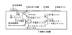
図1は本発明に係るCCDラインセンサ6を用いた画像入力装置1の構成を示す。画像入力装置1は解像度に応じた走査ライン間隔で原稿の画像情報を読み取る装置である。
FIG. 1 shows a configuration of an
原稿Dは原稿台ガラス2上に画像面を下向きにして置かれる。スタート釦(図示せず)が押されると、キセノン光源や冷陰極管等を用いた光源11が点灯し、そのときの照射光が原稿ガラス2を透過し、原稿Dの読み取り位置Xに照射される。原稿Dの読み取り位置Xからの反射光が第1ミラー12で反射し、第1ミラー12からの反射光が第2ミラー41、第3ミラー42に照射される。第2ミラー41と第3ミラー42で反射した原稿からの反射光は集光レンズ5に入射し、CCDラインセンサ6の受光面で結像する。CCDラインセンサ6は原稿Dを主走査方向に走査する。CCD基板7は前記CCDラインセンサ6の他に、CCDラインセンサ6を駆動するCCDドライバが実装されている。処理基板8にはCCDラインセンサ6から出力される画像信号を処理する電気回路及び画像入力装置1を総合的に制御するCPU等の処理回路(後述されるスキャナ制御部40)が実装されている。CCD基板7と処理基板(スキャナ制御部)40はハーネス9により接続されている。
The document D is placed on the
原稿Dを読み取る場合は、光源11と第1ミラー12で構成する第1キャリジ13と、第2ミラー41と第3ミラー42で構成する第2キャリジ4を、図中の矢印の方向に図示しない駆動モータ及びベルトまたはワイヤ等から構成される駆動系により移動する。これにより、読み取り位置Xが図中の左から右に移動して、原稿Dは副走査方向に走査される。このとき、第1キャリジ13の移動速度を2V、第2キャリジ4の移動速度をVというように、第1キャリジ13の移動速度を第2キャリジ4の2倍の移動速度とする。
When reading the document D, the first carriage 13 composed of the
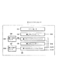
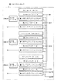
図2は画像入力装置1の制御系の構成を示すブロック図である。この画像入力装置1はスキャナ制御部40及びコントロールパネル部80を含む。
スキャナ制御部40は、CPU100、ROM101、RAM102、CCDドライバ103、スキャナモータドライバ104、画像処理部105、光源12を制御する光源制御部106、原稿自動検知部107を含んでいる。
FIG. 2 is a block diagram showing the configuration of the control system of the
The
CPU100はROM101に記憶された制御プログラムに従って、スキャナ制御部40を全体的に制御し、RAM102をデータの一時記憶用に用いる。CCDドライバ(CCD制御部)103はCCDラインセンサ6に各種CCD制御信号を送信し、CCDラインセンサ6を駆動する。スキャナモータドライバ104は第1及び第2のキャリッジ3及び4等を移動する駆動モータの回転を制御する。原稿自動検出部107によって原稿台ガラス2上に置かれた原稿が、カラー原稿であるかモノクロ原稿であるか及び原稿サイズを自動検知される。
The
画像処理部105はCCDラインセンサ6からのアナログ信号をディジタル信号に変換するA/D変換回路と周囲の温度変化などに起因するCCDラインセンサ6からの出力信号に対するスレッショルドレベルの変動を補正するためのシェーディング補正回路やガンマ補正回路を含む。また画像処理部105はこれら補正回路からの補正されたディジタル信号を一旦記憶するラインメモリを含む。更に画像処理部105は補正された画像データに対して、トリミング、マスキング、拡大/縮小処理、解像度変換、画像の圧縮/非圧縮処理等の画像処理を行う。
The
コントロールパネル部80はキーパッド82、パネルCPU83、液晶表示部84、コントロールパネル用I/F85を含む。パネルCPU83はコントロールパネルI/F85を介してCPU100と通信を行う。液晶表示部84には原稿読取り条件の設定画面等が表示され、パネルCPU83はキーパッド82を介してユーザからキー入力される原稿読取り条件に関するデータを受信し、該キー入力データをスキャナ制御部40に転送すると共に液晶表示部84に表示する。この原稿読取り条件には原稿をカラー原稿として読取るか、あるいはモノクロ原稿として読取るかの情報、及び解像度の情報等が含まれる。
The
以下、本発明による幾つかの実施形態を説明するが、何れの実施形態も、画像入力装置の基本構成は図1及び図2に示す構成と同様の構成を有している。 Several embodiments according to the present invention will be described below. In any of the embodiments, the basic configuration of the image input apparatus has the same configuration as that shown in FIGS. 1 and 2.
次に、CCDラインセンサ6の出力信号について説明する。
Next, the output signal of the
CCDラインセンサ6の出力信号波形は、所定オフセット電圧から基準電圧である0V方向に入射光量に比例した電圧値として現れる。
The output signal waveform of the
また、CCDラインセンサ6の光電変換部はフォトダイオードアレイで構成され、各フォトダイオードは光電変換効率が均一でない。この不均一性は、CCDラインセンサ6では出力電圧不均一性として定義してあり、CCDラインセンサ6からの出力信号の高周波歪みと考えられる。また、図1のような縮小光学系では集光レンズ5を用いているためレンズの収差が発生する。この収差のためにCCDラインセンサ6の受光面の両端の受光量が受光面の中央部に対し減少する。これを前記の高周波歪みに対して低周波歪みと記す。
Further, the photoelectric conversion unit of the
よって、CCDラインセンサ6の後段に設ける処理回路では、上記オフセット電圧や高周波歪みと低周波歪みを補正する必要がある。CCDラインセンサ6の後段にコンデンサを直列に接続することでCCDレベルであるオフセット電圧が除去され、さらに上記コンデンサの電位を設定することでオフセット電圧が所望の電圧に固定される。CCDラインセンサ6に光が照射しない状態での信号電位を黒レベルの基準として考え、その信号電位を上記オフセット電圧が除去された後の所望の電圧として設定する場合もある。
Therefore, the processing circuit provided in the subsequent stage of the
その後、各画素の出力アナログ信号は、サンプルホールド処理が行なわれ、振幅が安定化される。サンプルされたアナログ信号の振幅はゲインアンプ、一般的にはプログラマブル・ゲイン・アンプ(PGAと記す)と呼ばれる増幅器により、後段のアナログデジタル変換器(以下、ADCと記す)の入力レンジにあった振幅に増幅される。振幅調整を行った信号はADCにより、システムにあった分解能のデジタル信号に変換される。このときADCに入力するアナログ信号はADCの入力レンジを越えてはいけないため、図1に示す白基準板19を読み取った時の画像信号を入力最大値として、前記PGAの増幅率が調整される。白基準板19の白は、白い原稿よりも反射率の高い白に設定されるので、前記調整の結果、どんな原稿が読まれてもADCの出力は飽和しない。 Thereafter, the output analog signal of each pixel is subjected to sample hold processing, and the amplitude is stabilized. The amplitude of the sampled analog signal is in accordance with the input range of the subsequent analog-to-digital converter (hereinafter referred to as ADC) by a gain amplifier, generally called a programmable gain amplifier (hereinafter referred to as PGA). Is amplified. The signal whose amplitude has been adjusted is converted by the ADC into a digital signal having a resolution suitable for the system. At this time, since the analog signal input to the ADC must not exceed the ADC input range, the amplification factor of the PGA is adjusted with the image signal when the white reference plate 19 shown in FIG. 1 is read as the maximum input value. . Since the white color of the white reference plate 19 is set to a white color having a higher reflectance than that of the white document, the output of the ADC does not saturate as a result of the adjustment no matter what document is read.
この状態で信号には前記高周波歪みと低周波歪みが必ず含まれてしまうため、その歪みを補正する目的で歪み補正(一般的にシェーディング補正と呼び、以下、SHD補正と記す)が必要となる。 In this state, the signal always includes the high-frequency distortion and the low-frequency distortion. Therefore, distortion correction (generally referred to as shading correction, hereinafter referred to as SHD correction) is required for correcting the distortion. .
補正の具体的な方法としては、光源11を消灯し、CCDラインセンサ6に光を照射しない状態で、ADCによりデジタル変換した画素信号を黒基準信号として保管する。次に光源11を点灯し、その状態で白基準板19を読み取った画素信号をADCでデジタル変換して白基準信号として保管する。一般的にはノイズ除去の目的で黒基準信号及び白基準信号は8ラインや16ライン分のように複数ラインを読み取り、その画素信号の平均値を利用する。
As a specific method of correction, the pixel signal digitally converted by the ADC is stored as a black reference signal in a state where the
読み取った原稿Dの画像信号は、画素単位で上記黒基準信号が減算され、係数が乗算される。この係数は、白基準信号が所望の値(例えば、8bit分解能では255)となる値である。この処理により上記高周波歪み及び低周波歪みを補正(SHD補正)した画像信号を得ることができる。以上が画像入力装置の基本的な動作である。 The read image signal of the document D is subtracted from the black reference signal in units of pixels and multiplied by a coefficient. This coefficient is a value at which the white reference signal takes a desired value (for example, 255 for 8-bit resolution). By this processing, an image signal in which the high frequency distortion and the low frequency distortion are corrected (SHD correction) can be obtained. The above is the basic operation of the image input apparatus.
次に、図3〜5を用いて本発明の説明を行う。 Next, the present invention will be described with reference to FIGS.
図3Aは本発明の1実施形態に係るCCDラインセンサ6の概略構成図、図3Bはタイミング説明図、図4はCCDラインセンサ6の内部構造、図5AはCCDラインセンサ6の内部動作説明図、図5Bはそのタイミング例を示す。尚、図4は光を受光する1つのフォトダイオードについての構造を示し、CCDラインセンサ6は複数のフォトダイオードが直線上に配置されている。
3A is a schematic configuration diagram of a
CCDラインセンサ6はフォトダイオードアレイからなるラインセンサ61と;ラインセンサ61の各フォトダイオードの光電変換機能で得られた電荷を同時に転送するための第1のシフトゲート62と;第1のシフトゲートを介して転送された電荷をシフトクロックCLK1、CLK2に応じて主走査方向にシフトし、シフトされた画像信号を提供する第1のアナログシフトレジスタ63と;第1のアナログシフトレジスタ63のシフトされた画像信号を増幅し順次外部に提供する第1の出力アンプ64と;前記第1のアナログシフトレジスタ63に転送された電荷を更に同時に転送するための第2のシフトゲート65と;第2のシフトゲートを介して転送された電荷をシフトクロックCLK1、CLK2に応じて主走査方向にシフトし、シフトされた画像信号を提供する第2のアナログシフトレジスタ66と;第2のアナログシフトレジスタ66のシフトされた出力信号を増幅し順次外部に提供する第2の出力アンプ67から構成される。
The
ラインセンサ61に光エネルギー(hv)が照射され、光電変換機能により光エネルギーが電荷となりラインセンサ61に蓄えられる。このとき第1のシフトゲート62に印加される駆動信号SH1は“L”レベルで、ゲートは上に上がった状態となっている(図4、図5BのT1の状態)。
The
次に、信号SH1が“H”となることで第1のシフトゲート62が下がり、ラインセンサ61の電荷は第1のシフトゲート62を通過し第1のアナログシフトレジスタ63に転送される(図5A及び5B、T2の状態)。信号SH1を十分な時間(t1)“H”レベルとすることでラインセンサ61の電荷は全て第1のアナログシフトレジスタ63に転送される。その後、信号SH1を“L”に切り替える(T3の状態)。
Next, when the signal SH1 becomes “H”, the
次に、信号SH2を“L”レベルから“H”レベルとすることで第2のシフトゲート65が下がり第1のアナログシフトレジスタ63に転送された電荷が第2のシフトゲート65を通過し、第2のアナログシフトレジスタ66に転送される(T4の状態)。第1のアナログシフトレジスタ63に所望の電荷が残留する時間(t2)だけ経過した後に信号SH2を“L”レベルに戻す(T5の状態)。
Next, by changing the signal SH2 from the “L” level to the “H” level, the
以上のように第2のシフトゲート62の電荷転送時間(シフトパルス信号SH2のパルス幅)を調整することで、第1のアナログシフトレジスタ63の電荷量を容易に調整することが可能となる。尚、信号SH1、SH2はCCD制御部103により生成される。CCD制御部103により信号SH2のパルス幅が制御されることにより、光源11の光量バラツキ、ラインセンサ61(フォトダイオードアレイ)の感度バラツキが補正される。つまりCCD制御部103は、第1のアナログシフトレジスタ63上の電荷量を調整する。また、この電荷量調整は上記のように信号SH2の“H”レベル時間幅t2を変更しても、SH2′のように微小パルスの数を制御しても良い。
As described above, by adjusting the charge transfer time of the second shift gate 62 (the pulse width of the shift pulse signal SH2), the charge amount of the first
図6はシフトパルス信号の”H”レベル期間と残像量の関係の一例を示す。 FIG. 6 shows an example of the relationship between the “H” level period of the shift pulse signal and the afterimage amount.
横軸はシフトゲート駆動信号の有効時間幅(上記説明では信号SH2の“H”レベル期間すなわちパルス幅)、縦軸はアナログシフトレジスタに残留する残像量(上記説明では、第1のアナログシフトレジスタ63の残留電荷量)を示す。図6からも明らかなように、シフトゲートに印加するシフトパルス信号のパルス幅を制御することにより、電荷の転送量を容易に制御できることがわかる。尚、この図において”H”レベルのシフトパルスがシフトゲートに印加される前(信号SHが”H”レベル期間:0nS)のフォトダイオード出力レベルは800mVである。 The horizontal axis represents the effective time width of the shift gate drive signal (in the above description, the “H” level period or pulse width of the signal SH2), and the vertical axis represents the amount of residual image remaining in the analog shift register (in the above description, the first analog shift register). 63). As is apparent from FIG. 6, it is understood that the charge transfer amount can be easily controlled by controlling the pulse width of the shift pulse signal applied to the shift gate. In this figure, the photodiode output level is 800 mV before the “H” level shift pulse is applied to the shift gate (the signal SH is in the “H” level period: 0 nS).
図3に戻り、CCDラインセンサ6のタイミングについて説明する。
Returning to FIG. 3, the timing of the
CCDラインセンサ6の駆動信号は、ラインセンサ61の電荷を第1のアナログシフトレジスタ63に転送するために、第1のシフトゲート62に印加するシフトパルス信号SH1と;第1のアナログシフトレジスタ63の電荷を第2のアナログシフトレジスタ66に転送するために、第2のシフトゲート65に印加するシフトパルス信号SH2と、第1のアナログシフトレジスタ63または第2のアナログシフトレジスタ66に転送された電荷を順次第1の出力アンプ64または第2の出力アンプ67に転送するための転送クロックCLK1(φ1)及びCLK2(φ2)である。転送クロックCLK1(φ1)及びCLK2(φ2)は、第1のアナログシフトレジスタ63と第2のアナログシフトレジスタ66の両方に印加される。
The drive signal for the
また、第1のシフトゲート62または第2のシフトゲート65を電荷が通過して第1のアナログシフトレジスタ63または第2のアナログシフトレジスタ66に電荷を転送している際に、アナログシフトレジスタが動作しているとラインセンサ61上の電荷がアナログシフトレジスタの複数の画素部分に振りまかれてしまう。従って、信号SH1またはSH2が“H”レベルの時は前記転送クロックCLK1及びCLK2は停止する必要がある。
In addition, when the charge passes through the
図7に他の実施形態を示す。この実施形態は、CCDラインセンサ6を用いて写真画像等の階調を有する画像の階調性を向上する階調処理回路108である。図7Aは階調処理回路108の概略構成を示す。階調処理回路108はラインメモリ81及び画素合成回路82からなる。
FIG. 7 shows another embodiment. This embodiment is a
図3Aの第1の出力アンプ64から出力されたアナログ信号OS1は画像処理部105により、前記オフセット除去やサンプルホールド等のアナログ関連の各種処理が行われ、ADCによりデジタル信号に変換され、前記SHD補正により正規化され、その後、画素合成回路82に入力される。
The analog signal OS1 output from the
図3Aの第2の出力アンプ67から出力されたアナログ信号OS2も同様に、前記オフセット除去やサンプルホールド等のアナログ関連の各種処理が行われ、ADCによりデジタル信号に変換され、前記SHD補正により正規化され、その後、ラインメモリ81によって前記第1の出力アンプ64から出力される画像信号系OS1の流れに対し1ライン遅延される。
Similarly, the analog signal OS2 output from the
図7Bのように、画素合成回路82は入力画像信号を画素毎に加算する。この図において、例えば”(N−1)・1”は(N−1)番目ラインの第1画素である。ラインメモリ81から出力される画像信号は上記の通り1ライン遅延されている。画素合成回路82は第1の出力アンプ64のNライン目の画像信号と、ラインメモリ81から出力されるN−1ライン目の画像信号を加算する。以上の処理により、容易に読み取り方向(副走査方向)の画素を加算平均した画像信号を生成することができる。即ち、階調のある写真画像等の画像の階調性を向上できる。
As shown in FIG. 7B, the
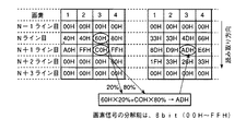
図7Cは読み取った画像信号を第2のシフトゲート65の駆動信号SH2のパルス幅制御により、80%の電荷を第1のアナログシフトレジスタ63へ、20%の電荷を第2のアナログシフトレジスタ66へ転送した場合を示す。
FIG. 7C shows that the read image signal is subjected to pulse width control of the drive signal SH2 for the
従来のCCDラインセンサで読み取った場合のNライン目3画素目の画像信号を“60H”、N+1ライン目3画素目の画像信号を“C0H”とする。本発明を用いるとN+1ライン目3画素目の画像信号は“ADH”(60H×20%+C0H×80%=ADH)となり、容易に画素の平均化処理が行える。 Assume that the image signal of the third pixel on the Nth line when read by the conventional CCD line sensor is “60H”, and the image signal of the third pixel on the N + 1th line is “C0H”. When the present invention is used, the image signal of the third pixel in the (N + 1) th line is “ADH” (60H × 20% + C0H × 80% = ADH), and the pixel averaging process can be easily performed.
上記の説明ではNライン目とN+1ライン目の割合を20:80としたが、第2のシフトゲート65に印加する信号SH2の“H”レベルを制御することで容易に上記の割合を変更することができる。
In the above description, the ratio of the Nth line and the (N + 1) th line is set to 20:80. However, the ratio can be easily changed by controlling the “H” level of the signal SH2 applied to the
次に、図8を用いて別の実施形態を説明する。 Next, another embodiment will be described with reference to FIG.
本実施形態は、光源11の発光色を切り替えることで、モノクロ用のCCDラインセンサ6を用いてカラー原稿を読み取る光源切り替え型カラー画像入力装置である。
The present embodiment is a light source switching type color image input device that reads a color document using a monochrome
画像入力装置の概要は図1に示した通りで、異なる点は光源11がREDの分光特性を有する光源11Rと、GREENの分光特性を有する光源11Gと、BLUEの分光特性を有する光源11Bの3つの光源で構成している点である。
The outline of the image input apparatus is as shown in FIG. 1 except that the
図8Aに概略構成図、図8Bにタイミング説明図を示す。 FIG. 8A is a schematic configuration diagram, and FIG. 8B is a timing diagram.
CCDラインセンサ6Aはフォトダイオードアレイからなるラインセンサ6A1と;第1のアナログシフトレジスタ6A3と;ラインセンサ6A1の光電変換機能で得られた電荷を、第1のアナログシフトレジスタ6A3に転送するためのゲートの役割をする第1のシフトゲート6A2と;第1のアナログシフトレジスタ6A3の電荷を順次増幅して外部に出力するための第1の出力アンプ6A4と;第2のアナログシフトレジスタ6A6と;第1のアナログシフトレジスタ6A3に転送された電荷を更に第2のアナログシフトレジスタ6A6に転送するための第2のシフトゲート6A5と;第2のアナログシフトレジスタ6A6の電荷を順次増幅して外部に出力するための第2の出力アンプ6A7と;第3のアナログシフトレジスタ6A6と;第2のアナログシフトレジスタ6A6に転送された電荷を更に第3のアナログシフトレジスタ6A9に転送するための第3のシフトゲート6A8と;第3のアナログシフトレジスタ6A9の電荷を順次増幅して外部に出力するための第3の出力アンプ6A10とから構成される。 The CCD line sensor 6A includes a line sensor 6A1 including a photodiode array; a first analog shift register 6A3; and a charge obtained by the photoelectric conversion function of the line sensor 6A1 for transferring to the first analog shift register 6A3. A first shift gate 6A2 serving as a gate; a first output amplifier 6A4 for sequentially amplifying the charges of the first analog shift register 6A3 and outputting them to the outside; a second analog shift register 6A6; A second shift gate 6A5 for further transferring the charge transferred to the first analog shift register 6A3 to the second analog shift register 6A6; and sequentially amplifying the charge of the second analog shift register 6A6 to the outside A second output amplifier 6A7 for outputting; a third analog shift register 6A6 A third shift gate 6A8 for further transferring the charge transferred to the second analog shift register 6A6 to the third analog shift register 6A9; and amplifying the charge of the third analog shift register 6A9 sequentially to externally And a third output amplifier 6A10.
図9A及び9Bは本実施形態の内部動作説明図である。 9A and 9B are explanatory diagrams of the internal operation of the present embodiment.
ラインセンサ6A1(フォトダイオード)に光エネルギー(hv)が照射され、光電変換機能により光エネルギーが電荷となりラインセンサ6A1に蓄えられる。このとき第1のシフトゲート6A2に印加される駆動信号SH1Aは“L”レベルで、ゲートは上に上がった状態となっている(図9BのT11の状態)。 The line sensor 6A1 (photodiode) is irradiated with light energy (hv), and the light energy is converted into electric charges by the photoelectric conversion function and stored in the line sensor 6A1. At this time, the drive signal SH1A applied to the first shift gate 6A2 is at the “L” level, and the gate is in an upward state (state T11 in FIG. 9B).
次に、信号SH1Aが“H”となることで第1のシフトゲート6A2が下がり、ラインセンサ6A1の電荷は第1のシフトゲート6A2を通過し第1のアナログシフトレジスタ6A3に転送される(図9A及び9BのT12の状態)。信号SH1を十分な時間(t1)“H”レベルとすることでラインセンサ6A1の電荷は全て第1のアナログシフトレジスタ6A3に転送される。その後、信号SH1Aを“L”に切り替える(T13の状態)。 Next, when the signal SH1A becomes “H”, the first shift gate 6A2 is lowered, and the charge of the line sensor 6A1 passes through the first shift gate 6A2 and is transferred to the first analog shift register 6A3 (FIG. 9A and 9B T12 state). By setting the signal SH1 to the “H” level for a sufficient time (t1), all charges of the line sensor 6A1 are transferred to the first analog shift register 6A3. Thereafter, the signal SH1A is switched to “L” (state of T13).
次に、信号SH2Aを“L”レベルから“H”レベルとすることで第2のシフトゲート6A5が下がり、第1のアナログシフトレジスタ6A3に転送された電荷が第2のシフトゲート6A5を通過し、第2のアナログシフトレジスタ6A6に転送される(T14の状態)。第1のアナログシフトレジスタ6A3の電荷が全て第2のアナログシフトレジスタ6A6に転送される時間(t2)だけ経過した後に信号SH2Aを“L”レベルに戻す(T15の状態)。 Next, by changing the signal SH2A from the “L” level to the “H” level, the second shift gate 6A5 is lowered, and the charge transferred to the first analog shift register 6A3 passes through the second shift gate 6A5. Are transferred to the second analog shift register 6A6 (state of T14). The signal SH2A is returned to the “L” level after the time (t2) when all the charges in the first analog shift register 6A3 are transferred to the second analog shift register 6A6 has elapsed (state of T15).
次に、信号SH3Aを“L”レベルから“H”レベルとすることで第3のシフトゲート6A8が下がり、第2のアナログシフトレジスタ6A6に転送された電荷が第3のシフトゲート6A8を通過し第3のアナログシフトレジスタ6A9に転送される(T16の状態)。第2のアナログシフトレジスタ6A6の電荷が全て第3のアナログシフトレジスタ6A9に転送される時間(t3)だけ経過した後に信号SH3Aを“L”レベルに戻す(T17の状態)。 Next, by changing the signal SH3A from the “L” level to the “H” level, the third shift gate 6A8 is lowered, and the charge transferred to the second analog shift register 6A6 passes through the third shift gate 6A8. Transferred to the third analog shift register 6A9 (state of T16). The signal SH3A is returned to the “L” level after the time (t3) when all the charges of the second analog shift register 6A6 are transferred to the third analog shift register 6A9 has elapsed (state of T17).
本発明の構成を用いたCCDラインセンサ6Aを光源切り替え型カラー画像入力装置に適応した場合の光源11(光源11R,11G,11B)の切り替えタイミングを図8Bに示す。光源11R、11G、11BのON/OFF制御は光源制御部106が行い、信号SH1A,SH2A,SH3AはCCD制御部103が生成する。
FIG. 8B shows the switching timing of the light source 11 (
光源11Bを図のタイミングで点灯し、第1のシフトゲート6A2に制御信号(シフトパルス)SH1Aを印加することで、光源11Bによる画像信号(B)が第1のアナログシフトレジスタ6A3(R)に転送される。上記制御信号SH1Aをt21で“H”レベルとし、”H”レベルの期間中に光源11Bを消灯し、光源11Gを点灯する。続いて、第2のシフトゲート6A5に制御信号SH2Aを印加することで、第1のアナログシフトレジスタ6A3(R)に転送された電荷が第2のアナログシフトレジスタ6A6(G)に転送される。続いて、第3のシフトゲート6A8に制御信号SH3Aを印加することで、第2のアナログシフトレジスタ6A6(G)に転送された電荷が第3のアナログシフトレジスタ6A9(B)に転送される。この制御によって、光源11Bで読み取った画像信号(B)は、全て第3のアナログシフトレジスタ6A9(B)に転送される。
The light source 11B is turned on at the timing shown in the figure, and the control signal (shift pulse) SH1A is applied to the first shift gate 6A2, whereby the image signal (B) from the light source 11B is supplied to the first analog shift register 6A3 (R). Transferred. The control signal SH1A is set to the “H” level at t21, the light source 11B is turned off during the “H” level period, and the
次に、第1のシフトゲート6A2に制御信号SH1Aを時刻t22から印加することで、光源11Gによる画像信号(G)が第1のアナログシフトレジスタ6A3(R)に転送される。上記制御信号SH1Aが“H”レベルの期間に光源11Gを消灯し、光源11Rを点灯する。続いて、第2のシフトゲート6A5に制御信号SH2Aの”H”レベルを印加することで、第1のアナログシフトレジスタ6A3(R)に転送された電荷が、全て第2のアナログシフトレジスタ6A6(G)に転送される。この制御によって、光源11Gにより読み取った画像信号(G)は第2のアナログシフトレジスタ6A6(G)に全て転送される。
Next, by applying the control signal SH1A to the first shift gate 6A2 from time t22, the image signal (G) from the
次に、第1のシフトゲート6A2に制御信号SH1Aの”H”レベルを時刻t23から印加することで、光源11Rによる画像信号(R)が第1のアナログシフトレジスタ6A3(R)に転送される。上記制御信号SH1Aが“H”レベルの期間に光源11Gを消灯し、光源11Bを点灯する。
Next, by applying the “H” level of the control signal SH1A to the first shift gate 6A2 from time t23, the image signal (R) from the light source 11R is transferred to the first analog shift register 6A3 (R). . The
以上が1サイクルの動作で、この動作により、第1のアナログシフトレジスタ6A3にはRED画像信号、第2のアナログシフトレジスタ6A6にはGREEN画像信号、第3のアナログシフトレジスタ6A9にはBLUEの画像信号が転送される。この1サイクルは例えば1mS程度で、この間に原稿の1ライン分のカラー情報がサンプルされる。 The above is the operation of one cycle. With this operation, the first analog shift register 6A3 has a RED image signal, the second analog shift register 6A6 has a GREEN image signal, and the third analog shift register 6A9 has a BLUE image signal. The signal is transferred. This one cycle is about 1 mS, for example, and color information for one line of the original is sampled during this period.
各アナログシフトレジスタに転送された電荷は、転送クロックCLK1A,CLK2Aにより順次出力アンプ6A4,6A7,6A10からCCDラインセンサ6Aの画像処理部105に出力される。
The charges transferred to each analog shift register are sequentially output from the output amplifiers 6A4, 6A7, 6A10 to the
上記説明では光源11を光源11B、光源11G、光源11Rの順番に点灯/消灯制御を行ったが、順番を変更しても問題ないが、その際は出力アンプから出力される信号の色情報が変わる。
In the above description, the
図8Bのタイミングで転送クロックCLK1A,CLK2Aを印加した場合は、図のように各色の画像情報は時間軸がずれて出力される。しかし、図10に示すように、1サイクルの動作のうち、制御信号SH1Aの3つ目の印加後のみに転送クロックCLK1A,CLK1Bを入力することで、各色の画像情報は同時に出力することができる。 When the transfer clocks CLK1A and CLK2A are applied at the timing of FIG. 8B, the image information of each color is output with the time axis shifted as shown. However, as shown in FIG. 10, by inputting the transfer clocks CLK1A and CLK1B only after the third application of the control signal SH1A in one cycle of operation, the image information of each color can be output simultaneously. .
次に本発明の他の実施形態を説明する。本実施形態はCCDラインセンサ6Aをモノクロ読取り動作に適用した例である。CCDラインセンサ6Aの構成は図8Aと同一であるので図示を省略する。 Next, another embodiment of the present invention will be described. This embodiment is an example in which the CCD line sensor 6A is applied to a monochrome reading operation. The configuration of the CCD line sensor 6A is the same as that shown in FIG.
本実施形態において、CCD制御部103は図11に示すように、上記制御信号SH1AのみをCCDラインセンサ6Aに供給し、制御信号SH2A,SH3Aは“L”レベルに固定される。従って、第1のアナログシフトレジスタ6A3の後段の第1の出力アンプ6A4からの出力信号のみが画像処理部105に出力される。
In the present embodiment, as shown in FIG. 11, the
この場合、光源11Rまたは光源11Gまたは光源11Bのみを点灯した読み取りでは、読み取り原稿はモノクロまたは単色原稿となる。白と黒画像で構成したモノクロ原稿の読み取りに関しては問題は生じない。
In this case, in reading with only the light source 11R, the
光源11R、光源11G、光源11Bの全てを同時に点灯することで、上記原稿を構成する色によって読みにくいという問題は無くなり、かつCCDラインセンサ6Aに入射する光量が増加するため読み取り速度の向上を図ることも可能である。
By turning on all of the light source 11R, the
図12に3ラインCCDセンサに本発明を適用した実施形態の構成例を示す。図12は図3Aに対して次の点が異なる。即ち、R.G.B.用ラインセンサを設けてそれぞれのラインセンサに対して、第1及び第2のシフトゲートと出力段アンプと第1及び第2のアナログシフトレジスタを設けている。 FIG. 12 shows a configuration example of an embodiment in which the present invention is applied to a three-line CCD sensor. FIG. 12 differs from FIG. 3A in the following points. That is, R.I. G. B. For each line sensor, first and second shift gates, an output stage amplifier, and first and second analog shift registers are provided.
3ラインCCDセンサ6Bは、各ラインセンサの受光面にR、G、Bの色フィルタが配置されている。 In the 3-line CCD sensor 6B, R, G, and B color filters are arranged on the light receiving surface of each line sensor.
ラインセンサの出力電圧は、光源の分光分布特性とラインセンサの分光感度特性の積となる。従って、光源と該光源の特性に適したラインセンサを選別することによって、基準となる原稿、例えば、図1に示した白基準板19を読取った際の各色のラインセンサの出力電圧を一致させることは可能である。例えば、光源のR、G、B各蛍光剤の量を調節することにより、R、G、B用のラインセンサの出力電圧を一致させることが可能である。しかし、前記従来技術にも記載したが、CCDラインセンサの分光感度特性や光源の分光分布特性、また、光源の光量は一般に各デバイスについてバラツキを有している。従って、光源と該光源の特性に最適なCCDラインセンサを選別するのは容易ではない。 The output voltage of the line sensor is the product of the spectral distribution characteristic of the light source and the spectral sensitivity characteristic of the line sensor. Accordingly, by selecting a light source and a line sensor suitable for the characteristics of the light source, the output voltages of the line sensors for the respective colors when the original document, for example, the white reference plate 19 shown in FIG. It is possible. For example, the output voltages of the R, G, and B line sensors can be matched by adjusting the amounts of the R, G, and B fluorescent agents of the light source. However, as described in the above prior art, the spectral sensitivity characteristic of the CCD line sensor, the spectral distribution characteristic of the light source, and the light quantity of the light source generally vary for each device. Therefore, it is not easy to select a light source and a CCD line sensor optimal for the characteristics of the light source.
本実施形態において、CCD制御部103はRED用の第2のアナログシフトレジスタRへの電荷転送信号(シフトパルス)SHRと、GREEN用の第2のアナログシフトレジスタGへの電荷転送信号SHGと、BLUE用の第2アナログシフトレジスタBへの電荷転送信号SHBのパルス幅が、各ラインセンサの感度に応じて変更される。これにより、RED用の第1のアナログシフトレジスタRとGREEN用の第1のアナログシフトレジスタGとBLUE用の第1のアナログシフトレジスタB上の電荷量が調整される。従って、RED出力(OSR)とGREEN出力(OSG)とBLUE出力(OSB)の信号振幅を容易に合わせることができる。
In the present embodiment, the
図12では、ラインセンサをRED,GREEN,BLUEの順番に配置したが、必ずしも上記順番である必要は無い。 In FIG. 12, the line sensors are arranged in the order of RED, GREEN, and BLUE.
図13は4ラインCCDセンサに本発明を適用した実施形態の構成図を示す。図13の4ラインCCDセンサ6Cは、図12の3ラインCCDセンサ6Bに対してBLACK用ラインセンサBLACKと、該BLACK用ラインセンサに関する第1及び第2のシフトゲートKと出力段アンプKと第1及び第2のアナログシフトレジスタKを設けた例である。 FIG. 13 shows a configuration diagram of an embodiment in which the present invention is applied to a 4-line CCD sensor. The 4-line CCD sensor 6C in FIG. 13 is different from the 3-line CCD sensor 6B in FIG. 12 in that the BLACK line sensor BLACK, the first and second shift gates K, the output stage amplifier K, and the In this example, the first and second analog shift registers K are provided.
前述したように、光源とCCDラインセンサを合わせ込みことによって、基準となる原稿、例えば、図1に示した白基準板19を読取った際のCCDラインセンサの各色の出力電圧を一致させることは可能である。しかし、各デバイスはバラツキを有しているので、光源と該光源の特性に最適なCCDラインセンサを選別するのは容易ではない。 As described above, by combining the light source and the CCD line sensor, it is possible to match the output voltages of the respective colors of the CCD line sensor when the reference original, for example, the white reference plate 19 shown in FIG. 1 is read. Is possible. However, since each device has variations, it is not easy to select a light source and a CCD line sensor optimal for the characteristics of the light source.
本実施形態においても、CPU制御部103はRED用の第2のアナログシフトレジスタRへの電荷転送信号SHRと、GREEN用の第2のアナログシフトレジスタGへの電荷転送信号SHGと、BLUE用の第2アナログシフトレジスタBへの電荷転送信号SHBのパルス幅を各ラインセンサの感度に応じて変更する。
Also in this embodiment, the
上記ラインセンサは受光面に色フィルタが配置されるが、4ラインCCDセンサ6CのラインセンサBLACKの受光面は、上記色フィルタではなく無色透明の保護プレートが配置される。従って、ラインセンサBLACKの感度は他のCCDラインセンサに比べ大きい。4ラインCCDセンサでは、各ラインCCDセンサの受光面サイズが同一の場合、BLACK出力(OSK)が他の信号よりも振幅が大きくなる傾向がある。 In the line sensor, a color filter is disposed on the light receiving surface, but a colorless and transparent protective plate is disposed on the light receiving surface of the line sensor BLACK of the 4-line CCD sensor 6C instead of the color filter. Therefore, the sensitivity of the line sensor BLACK is higher than that of other CCD line sensors. In the 4-line CCD sensor, when the light-receiving surface size of each line CCD sensor is the same, the BLACK output (OSK) tends to have a larger amplitude than other signals.
従って本実施形態では、CCD制御部103はBLACK用の第2のシフトゲートKの制御信号のパルス幅を他の制御信号より短く設定する。このようにして、BLACKの出力信号OSKの振幅を、容易に他の出力信号OSR,OSG,OSBの振幅と同一にすることができる。尚、図13では、ラインセンサをRED,GREEN,BLUE,BLACKの順番に配置したが、必ずしも上記順番である必要は無い。
Therefore, in the present embodiment, the
以上、本発明を一次元CCDセンサに応用した例を説明したが、本発明の主旨は二次元CCDセンサにも適用できることは明らかである。 The example in which the present invention is applied to a one-dimensional CCD sensor has been described above, but it is obvious that the gist of the present invention can be applied to a two-dimensional CCD sensor.
また、以上の説明はこの発明の実施の形態であって、この発明の装置及び方法を限定するものではない。更に、各実施形態における構成要素、機能、特徴あるいは方法ステップを適宜組み合わせて構成される装置又は方法も本発明に含まれるものである。 The above description is an embodiment of the present invention and does not limit the apparatus and method of the present invention. Furthermore, an apparatus or a method configured by appropriately combining the components, functions, features, or method steps in each embodiment is also included in the present invention.
2…原稿ガラス、3…第1キャリッジ、4…第2キャリッジ、5…集光レンズ、6…CCDラインセンサ、7…CCD基板、9…ハーネス、11…光源、12…第1ミラー19…白基準板、40…処理基板、41…第2ミラー、42…第3ミラー。 2 ... Original glass, 3 ... 1st carriage, 4 ... 2nd carriage, 5 ... Condensing lens, 6 ... CCD line sensor, 7 ... CCD substrate, 9 ... Harness, 11 ... Light source, 12 ... 1st mirror 19 ... White Reference plate, 40 ... processing substrate, 41 ... second mirror, 42 ... third mirror.
Claims (4)
前記ラインセンサに蓄積された電荷を同時に転送するための第1のシフトゲートと、
前記第1のシフトゲートを介して電荷が転送され、転送された電荷をシフトクロックに応じて主走査方向にシフトし、シフトされた画像信号を提供する第1のアナログシフトレジスタと、
前記第1のアナログシフトレジスタの電荷を同時に転送するための第2のシフトゲートと、
前記第2のシフトゲートを介して電荷が転送され、転送された電荷を前記シフトクロックに応じて主走査方向にシフトし、シフトされた画像信号を提供する第2のアナログシフトレジスタと、
前記第2のシフトゲートの電荷転送時間を調整することで、前記第1のアナログシフトレジスタ上の電荷量を調整する調整部と、
前記第1のアナログシフトレジスタから提供される前記画像信号を処理する第1の画像処理部と、
前記第2のアナログシフトレジスタから提供される前記画像信号を処理する第2の画像処理部と、
前記第1の画像処理部により処理された画像信号を1ライン分遅延するラインメモリと、
前記第2の画像処理部により処理された画像信号と、前記ラインメモリにより遅延された画像信号を加算する加算部と、
を具備することを特徴とする画像入力装置。 A line sensor in which a plurality of photoelectric conversion elements are arranged on a straight line and accumulates charges corresponding to a received document image;
A first shift gate for simultaneously transferring charges accumulated in the line sensor;
A first analog shift register that transfers charges through the first shift gate, shifts the transferred charges in the main scanning direction according to a shift clock, and provides a shifted image signal;
A second shift gate for simultaneously transferring charges of the first analog shift register;
A second analog shift register that transfers charges through the second shift gate, shifts the transferred charges in the main scanning direction according to the shift clock, and provides a shifted image signal;
An adjustment unit for adjusting an amount of charge on the first analog shift register by adjusting a charge transfer time of the second shift gate;
A first image processing unit for processing the image signal provided from the first analog shift register;
A second image processing unit for processing the image signal provided from the second analog shift register;
A line memory that delays the image signal processed by the first image processing unit by one line;
An adder for adding the image signal processed by the second image processor and the image signal delayed by the line memory;
An image input apparatus comprising:
前記ラインセンサに蓄積された電荷を同時に転送するための第1のシフトゲートと、
前記第1のシフトゲートを介して電荷が転送され、転送された電荷をシフトクロックに応じて主走査方向にシフトし、シフトされた画像信号を提供する第1のアナログシフトレジスタと、
前記第1のアナログシフトレジスタの電荷を同時に転送するための第2のシフトゲートと、
前記第2のシフトゲートを介して電荷が転送され、転送された電荷を前記シフトクロックに応じて主走査方向にシフトし、シフトされた画像信号を提供する第2のアナログシフトレジスタと、
前記第2のシフトゲートの電荷転送時間を調整することで、前記第1のアナログシフトレジスタ上の電荷量を調整する調整部と、
前記第2のアナログシフトレジスタの電荷を同時に転送するための第3のシフトゲートと、
前記第3のシフトゲートを介して電荷が転送され、転送された電荷を前記シフトクロックに応じて主走査方向にシフトし、シフトされた画像信号を提供する第3のアナログシフトレジスタと、
赤、緑、青の分光特性をそれぞれ有し原稿を照明する3つの光源と、
前記第1のシフトゲートの電荷転送周期で、前記3つの光源を順次切り替えて点灯させる光源制御部と、
を具備することを特徴とする画像入力装置。 A line sensor in which a plurality of photoelectric conversion elements are arranged on a straight line and accumulates charges corresponding to a received document image;
A first shift gate for simultaneously transferring charges accumulated in the line sensor;
A first analog shift register that transfers charges through the first shift gate, shifts the transferred charges in the main scanning direction according to a shift clock, and provides a shifted image signal;
A second shift gate for simultaneously transferring charges of the first analog shift register;
A second analog shift register that transfers charges through the second shift gate, shifts the transferred charges in the main scanning direction according to the shift clock, and provides a shifted image signal;
An adjustment unit for adjusting an amount of charge on the first analog shift register by adjusting a charge transfer time of the second shift gate;
A third shift gate for simultaneously transferring charges of the second analog shift register;
A third analog shift register that transfers charges through the third shift gate, shifts the transferred charges in the main scanning direction according to the shift clock, and provides a shifted image signal;
Three light sources each having red, green, and blue spectral characteristics to illuminate the document;
A light source controller that sequentially switches and lights the three light sources in the charge transfer period of the first shift gate;
An image input apparatus comprising:
前記ラインセンサに蓄積された電荷を、第1のシフトゲートを介して第1のアナログシフトレジスタに同時に転送し、
前記第1のアナログシフトレジスタに転送された電荷をシフトクロックに応じて主走査方向にシフトし、シフトされた画像信号を提供し、
前記第1のアナログシフトレジスタに転送された電荷を、第2のシフトゲートを介して第2のアナログシフトレジスタに同時に転送し、
前記第2のアナログシフトレジスタに転送された電荷を前記シフトクロックに応じて主走査方向にシフトし、シフトされた画像信号を提供し、
前記第2のシフトゲートの電荷転送時間を調整することで、前記第1のアナログシフトレジスタ上の電荷量を調整し、
前記第1のアナログシフトレジスタから提供される前記画像信号を処理し、処理された画像信号をラインメモリにて1ライン分遅延し、
前記第2のアナログシフトレジスタから提供される前記画像信号を処理し、処理された画像信号と、前記ラインメモリにより遅延された画像信号を加算することを特徴とする画像入力方法。 In a line sensor in which a plurality of photoelectric conversion elements are arranged on a straight line, charges corresponding to the received document image are accumulated,
The charge accumulated in the line sensor is simultaneously transferred to the first analog shift register via the first shift gate;
The charge transferred to the first analog shift register is shifted in the main scanning direction according to a shift clock to provide a shifted image signal;
Simultaneously transferring the charge transferred to the first analog shift register to the second analog shift register via the second shift gate;
The charge transferred to the second analog shift register is shifted in the main scanning direction according to the shift clock, and a shifted image signal is provided.
Adjusting the amount of charge on the first analog shift register by adjusting the charge transfer time of the second shift gate;
Processing the image signal provided from the first analog shift register, delaying the processed image signal by one line in a line memory;
An image input method comprising: processing the image signal provided from the second analog shift register; and adding the processed image signal and the image signal delayed by the line memory .
Applications Claiming Priority (1)
| Application Number | Priority Date | Filing Date | Title |
|---|---|---|---|
| US10/391,623 US7327500B2 (en) | 2003-03-20 | 2003-03-20 | Image inputting apparatus |
Publications (3)
| Publication Number | Publication Date |
|---|---|
| JP2004289821A JP2004289821A (en) | 2004-10-14 |
| JP2004289821A5 JP2004289821A5 (en) | 2007-04-26 |
| JP4192111B2 true JP4192111B2 (en) | 2008-12-03 |
Family
ID=32987724
Family Applications (1)
| Application Number | Title | Priority Date | Filing Date |
|---|---|---|---|
| JP2004072763A Expired - Fee Related JP4192111B2 (en) | 2003-03-20 | 2004-03-15 | Image input device |
Country Status (2)
| Country | Link |
|---|---|
| US (1) | US7327500B2 (en) |
| JP (1) | JP4192111B2 (en) |
Families Citing this family (8)
| Publication number | Priority date | Publication date | Assignee | Title |
|---|---|---|---|---|
| JP2006093820A (en) * | 2004-09-21 | 2006-04-06 | Canon Inc | Linear image sensor, image reading apparatus, image reading method, and program |
| JP4692160B2 (en) * | 2005-08-29 | 2011-06-01 | セイコーエプソン株式会社 | Photoelectric conversion element inspection method, image reading apparatus, and program |
| US20080036847A1 (en) * | 2006-08-14 | 2008-02-14 | Kabushiki Kaisha Toshiba | Image Reading Apparatus, Image Forming Apparatus, and Image Reading Method |
| US8194297B2 (en) * | 2007-08-07 | 2012-06-05 | Canon Kabushiki Kaisha | Method for controlling linear sensor, and image reading apparatus |
| JP2010199945A (en) * | 2009-02-25 | 2010-09-09 | Seiko Epson Corp | Device for reading image, and method of controlling the same |
| JP5690783B2 (en) * | 2012-07-27 | 2015-03-25 | 京セラドキュメントソリューションズ株式会社 | Image reading apparatus and image forming apparatus |
| US9143696B2 (en) * | 2012-10-13 | 2015-09-22 | Hewlett-Packard Development Company, L.P. | Imaging using offsetting accumulations |
| JP6142815B2 (en) * | 2014-02-13 | 2017-06-07 | ブラザー工業株式会社 | Image reading device |
Family Cites Families (6)
| Publication number | Priority date | Publication date | Assignee | Title |
|---|---|---|---|---|
| US5499111A (en) * | 1991-08-06 | 1996-03-12 | Matsushita Graphic Communication Systems, Inc. | Image signal processing apparatus |
| JPH08163380A (en) * | 1994-12-09 | 1996-06-21 | Fujitsu Ltd | Method and device for image read |
| JPH1194696A (en) * | 1997-09-22 | 1999-04-09 | Ricoh Co Ltd | Ccd inspection device and method therefor |
| JP3964567B2 (en) | 1999-02-17 | 2007-08-22 | 東芝マイクロエレクトロニクス株式会社 | Solid-state imaging device |
| US6958835B2 (en) * | 2001-09-19 | 2005-10-25 | Kabushiki Kaisha Toshiba | Image inputting apparatus and image forming apparatus using four-line CCD sensor |
| US7339709B2 (en) * | 2003-03-04 | 2008-03-04 | Kabushiki Kaisha Toshiba | Method and apparatus for forming image |
-
2003
- 2003-03-20 US US10/391,623 patent/US7327500B2/en not_active Expired - Fee Related
-
2004
- 2004-03-15 JP JP2004072763A patent/JP4192111B2/en not_active Expired - Fee Related
Also Published As
| Publication number | Publication date |
|---|---|
| JP2004289821A (en) | 2004-10-14 |
| US7327500B2 (en) | 2008-02-05 |
| US20040184116A1 (en) | 2004-09-23 |
Similar Documents
| Publication | Publication Date | Title |
|---|---|---|
| US4985760A (en) | Color imager having varying filter aperture sizes to compensate for luminance differences between colors | |
| US7869086B2 (en) | Offset adjusting device, correcting device, and method of adjusting analog image signal | |
| US8004726B2 (en) | Image reading apparatus and image density correction method | |
| EP1137255B1 (en) | Correction method and apparatus for image signals obtained by an image sensor having a multiple output channels | |
| US8107137B2 (en) | 4-line CCD sensor and image input apparatus using the same | |
| JP4192111B2 (en) | Image input device | |
| JPH04363967A (en) | Original reader | |
| JPH0799850B2 (en) | Image reading device for image recording device | |
| US6445413B1 (en) | System for determining a video offset from dark photosensors in an image sensor array | |
| US9019581B2 (en) | Image processing apparatus and method | |
| JP2003230007A (en) | Image reader, its control method, and control program | |
| JPH1188898A (en) | Image reader | |
| JP3494462B2 (en) | Signal processing device | |
| JP5817312B2 (en) | Image reading apparatus and image forming apparatus | |
| JP2004007160A (en) | Shading correcting device | |
| JP4414276B2 (en) | Image reading device | |
| JPH0416087A (en) | Picture reader | |
| JP2003244453A (en) | Image reader | |
| JPH07154597A (en) | Image data adjustment method of image reader | |
| JPH08251407A (en) | Image reader | |
| JPH1155509A (en) | Image reader | |
| JP2002199213A (en) | Image reader | |
| JP2001217990A (en) | Image reader and image reading method | |
| JP2000125093A (en) | Digital copying machine | |
| JP2005094064A (en) | Image reading apparatus |
Legal Events
| Date | Code | Title | Description |
|---|---|---|---|
| A521 | Request for written amendment filed |
Free format text: JAPANESE INTERMEDIATE CODE: A523 Effective date: 20070312 |
|
| A621 | Written request for application examination |
Free format text: JAPANESE INTERMEDIATE CODE: A621 Effective date: 20070312 |
|
| A977 | Report on retrieval |
Free format text: JAPANESE INTERMEDIATE CODE: A971007 Effective date: 20080613 |
|
| A131 | Notification of reasons for refusal |
Free format text: JAPANESE INTERMEDIATE CODE: A131 Effective date: 20080624 |
|
| A521 | Request for written amendment filed |
Free format text: JAPANESE INTERMEDIATE CODE: A523 Effective date: 20080825 |
|
| TRDD | Decision of grant or rejection written | ||
| A01 | Written decision to grant a patent or to grant a registration (utility model) |
Free format text: JAPANESE INTERMEDIATE CODE: A01 Effective date: 20080916 |
|
| A01 | Written decision to grant a patent or to grant a registration (utility model) |
Free format text: JAPANESE INTERMEDIATE CODE: A01 |
|
| A61 | First payment of annual fees (during grant procedure) |
Free format text: JAPANESE INTERMEDIATE CODE: A61 Effective date: 20080919 |
|
| FPAY | Renewal fee payment (event date is renewal date of database) |
Free format text: PAYMENT UNTIL: 20110926 Year of fee payment: 3 |
|
| R150 | Certificate of patent or registration of utility model |
Free format text: JAPANESE INTERMEDIATE CODE: R150 |
|
| LAPS | Cancellation because of no payment of annual fees |