EP2551919A2 - Solarzellenbaugruppe - Google Patents
Solarzellenbaugruppe Download PDFInfo
- Publication number
- EP2551919A2 EP2551919A2 EP12005480A EP12005480A EP2551919A2 EP 2551919 A2 EP2551919 A2 EP 2551919A2 EP 12005480 A EP12005480 A EP 12005480A EP 12005480 A EP12005480 A EP 12005480A EP 2551919 A2 EP2551919 A2 EP 2551919A2
- Authority
- EP
- European Patent Office
- Prior art keywords
- electrode layer
- solar cells
- end portion
- solar cell
- cell assembly
- Prior art date
- Legal status (The legal status is an assumption and is not a legal conclusion. Google has not performed a legal analysis and makes no representation as to the accuracy of the status listed.)
- Withdrawn
Links
- 239000000758 substrate Substances 0.000 claims description 29
- 239000004065 semiconductor Substances 0.000 claims description 14
- 238000009792 diffusion process Methods 0.000 claims description 9
- 239000000463 material Substances 0.000 claims description 4
- 239000007769 metal material Substances 0.000 claims description 4
- 229910004613 CdTe Inorganic materials 0.000 claims description 3
- 229910052751 metal Inorganic materials 0.000 claims description 3
- 239000002184 metal Substances 0.000 claims description 3
- 229910052804 chromium Inorganic materials 0.000 claims description 2
- 229910052802 copper Inorganic materials 0.000 claims description 2
- 229910052737 gold Inorganic materials 0.000 claims description 2
- 229910052742 iron Inorganic materials 0.000 claims description 2
- 239000000203 mixture Substances 0.000 claims description 2
- 229910052759 nickel Inorganic materials 0.000 claims description 2
- 229910052709 silver Inorganic materials 0.000 claims description 2
- 239000010935 stainless steel Substances 0.000 claims description 2
- 229910001220 stainless steel Inorganic materials 0.000 claims description 2
- 229910052721 tungsten Inorganic materials 0.000 claims description 2
- 239000000956 alloy Substances 0.000 claims 1
- 229910045601 alloy Inorganic materials 0.000 claims 1
- 239000010410 layer Substances 0.000 description 29
- XLOMVQKBTHCTTD-UHFFFAOYSA-N Zinc monoxide Chemical compound [Zn]=O XLOMVQKBTHCTTD-UHFFFAOYSA-N 0.000 description 6
- 239000011787 zinc oxide Substances 0.000 description 3
- ZOKXTWBITQBERF-UHFFFAOYSA-N Molybdenum Chemical compound [Mo] ZOKXTWBITQBERF-UHFFFAOYSA-N 0.000 description 1
- 239000004642 Polyimide Substances 0.000 description 1
- 230000002411 adverse Effects 0.000 description 1
- 230000005540 biological transmission Effects 0.000 description 1
- 238000006243 chemical reaction Methods 0.000 description 1
- 239000004020 conductor Substances 0.000 description 1
- 239000011521 glass Substances 0.000 description 1
- AMGQUBHHOARCQH-UHFFFAOYSA-N indium;oxotin Chemical compound [In].[Sn]=O AMGQUBHHOARCQH-UHFFFAOYSA-N 0.000 description 1
- 238000004519 manufacturing process Methods 0.000 description 1
- 229910052750 molybdenum Inorganic materials 0.000 description 1
- 239000011733 molybdenum Substances 0.000 description 1
- 229920000728 polyester Polymers 0.000 description 1
- 229920001721 polyimide Polymers 0.000 description 1
- 239000011241 protective layer Substances 0.000 description 1
- 239000002699 waste material Substances 0.000 description 1
Images


Classifications
-
- H—ELECTRICITY
- H10—SEMICONDUCTOR DEVICES; ELECTRIC SOLID-STATE DEVICES NOT OTHERWISE PROVIDED FOR
- H10F—INORGANIC SEMICONDUCTOR DEVICES SENSITIVE TO INFRARED RADIATION, LIGHT, ELECTROMAGNETIC RADIATION OF SHORTER WAVELENGTH OR CORPUSCULAR RADIATION
- H10F19/00—Integrated devices, or assemblies of multiple devices, comprising at least one photovoltaic cell covered by group H10F10/00, e.g. photovoltaic modules
- H10F19/90—Structures for connecting between photovoltaic cells, e.g. interconnections or insulating spacers
- H10F19/902—Structures for connecting between photovoltaic cells, e.g. interconnections or insulating spacers for series or parallel connection of photovoltaic cells
-
- Y—GENERAL TAGGING OF NEW TECHNOLOGICAL DEVELOPMENTS; GENERAL TAGGING OF CROSS-SECTIONAL TECHNOLOGIES SPANNING OVER SEVERAL SECTIONS OF THE IPC; TECHNICAL SUBJECTS COVERED BY FORMER USPC CROSS-REFERENCE ART COLLECTIONS [XRACs] AND DIGESTS
- Y02—TECHNOLOGIES OR APPLICATIONS FOR MITIGATION OR ADAPTATION AGAINST CLIMATE CHANGE
- Y02E—REDUCTION OF GREENHOUSE GAS [GHG] EMISSIONS, RELATED TO ENERGY GENERATION, TRANSMISSION OR DISTRIBUTION
- Y02E10/00—Energy generation through renewable energy sources
- Y02E10/50—Photovoltaic [PV] energy
Definitions
- the invention relates to a solar cell assembly, and more particularly to a solar cell assembly including a plurality of solar cells that are partially stacked one above the other.
- U.S. Patent Application Publication No. 2011/0265849 discloses a solar cell panel that includes a plurality of solar cells 10, interconnectors 11 for electrically connecting in series the solar cells 10 to one another, and front and back protective layers (not shown) sandwiching the solar cells 10 and the interconnectors 11.
- the solar cell panel thus formed is disadvantageous in that an undesired gap 13 is formed between two adjacent ones of the solar cells 10, which results in a waste of space for the solar cell panel.
- the use of the interconnectors 11 in the solar cell panel increases the manufacturing costs.
- the object of the present invention is to provide a solar cell assembly that can overcome the aforesaid drawbacks associated with the prior art.
- a solar cell assembly that comprises a plurality of solar cells that are electrically connected to one another to form a series connection and that are aligned along an alignment direction.
- Each of the solar cells has opposite first and second end portions that are opposite to each other in the alignment direction.
- the first end portion of a subsequent one of the solar cells in the series connection is stacked on and is electrically connected to the second end portion of a preceding one of the solar cells in the series connection.
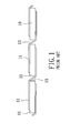
- Fig. 2 illustrates the first preferred embodiment of a solar cell assembly according to the present invention.
- the solar cell assembly includes a plurality of solar cells 3 that are electrically connected to one another to form a series connection and that are aligned along an alignment direction (X).
- Each of the solar cells 3 has opposite first and second end portions 301, 302 that are opposite to each other in the alignment direction (X).
- the first end portion 301 of a subsequent one of the solar cells 3 in the series connection is stacked on and is electrically connected to the second end portion 302 of a preceding one of the solar cells 3 in the series connection.
- each of the solar cells 3 includes a metallic substrate 311, a back electrode layer 312 formed on the metallic substrate 311, a top electrode layer structure 33 disposed at one side of the back electrode layer 312 opposite to the metallic substrate 311, and a semiconductor photovoltaic layer 32 disposed between the back electrode layer 312 and the top electrode layer structure 33 and defining a p-n junction (not shown) for conversion of an incident light into an electrical current.
- the metallic substrate 311 of each of the solar cells 3 has an end portion 311a corresponding to the first end portion 301 of the respective one of the solar cells 3.
- the top electrode layer structure 33 of each of the solar cells 3 has an end portion 33a corresponding to the second end portion 302 of the respective one of the solar cells 3.
- the end portion 311a of the metallic substrate 311 of each subsequent one of the solar cells 3 in the series connection is bonded to the end portion 33a of the top electrode layer structure 33 of the preceding one of the solar cells 3 in the series connection through a conductive paste (not shown).
- the metallic substrate 311 is flexible, and is made from a metallic material selected from Fe, Cr, Ni, and combinations thereof.
- the metallic substrate 311 is made from stainless steel having a composition comprising 60-77wt% of Fe, 15-32wt% of Cr, and 8-25wt% of Ni.
- the back electrode layer 312 is made from a metal, such as molybdenum (Mo).
- Mo molybdenum
- the semiconductor photovoltaic layer 32 is made from a semiconductor material selected from Si, CdTe, CuInSe, and CuInGaSe.
- the top electrode layer structure 33 includes a transparent current diffusion layer 331 formed on the semiconductor photovoltaic layer 32, and a transparent front electrode layer 332 formed on the current diffusion layer 331.
- the transparent current diffusion layer 331 is made from a transparent conductive material selected from indium tin oxide and zinc oxide, and has a layer thickness less than 0.05 ⁇ m.
- the transparent front electrode layer 332 is made from aluminum-doped zinc oxide (ZnO:Al), and has a layer thickness ranging from 0.5 ⁇ m -1.5 ⁇ m.
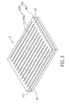
- Fig. 3 illustrates a solar cell 3' modified from the solar cell 3 of the first preferred embodiment.
- the solar cell 3' differs from the solar cell 3 of the first preferred embodiment in that the transparent front electrode layer 332 has a plurality of conductive strips 332a that are spaced apart from one another and that are made from a metallic material.
- Each of the conductive strips 332a of each of the solar cells 3' extends from the first end portion 301 to the second end portion 302 of the respective one of the solar cells 3' .
- the conductive strips 332a may be nontransparent.
- Fig. 4 illustrates the second preferred embodiment of the solar cell assembly according to thepresentinvention.
- Thesecond preferredembodiment differs from the previous preferred embodiment in that each of the solar cells 3 includes a non-conductive substrate 313 formed with a through-hole 3130, a back electrode layer 312 formed on the non-conductive substrate 313, a conductive connecting block 314 filling the through-hole 3130 and connected to the back electrode layer 312, a top electrode layer structure 33 disposed at one side of the back electrode layer 312 opposite to the non-conductive substrate 313, and a semiconductor photovoltaic layer 32 disposed between the back electrode layer 312 and the top electrode layer structure 33.
- the non-conductive substrate 313 of each of the solar cells 3 has an end portion 313a corresponding to the first end portion 301 of the respective one of the solar cells 3.
- the through-hole 3130 is formed in the end portion 313a of the non-conductive substrate 313.
- the top electrode layer structure 33 of each of the solar cells 3 has an end portion 33a corresponding to the second end portion 302 of the respective one of the solar cells 3.
- the end portion 313a of the non-conductive substrate 313 of each subsequent one of the solar cells 3 in the series connection together with the conductive connecting block 314 is bonded to the end portion 33a of the top electrode layer structure 33 of the preceding one of the solar cells 3 in the series connection.
- the non-conductive substrate 313 is made from glass or a polymeric material, such as polyimide or polyester.
- the conductive connecting block 314 is made from a metal selected from Au, Ag, Cu, and W.
Landscapes
- Photovoltaic Devices (AREA)
Applications Claiming Priority (1)
| Application Number | Priority Date | Filing Date | Title |
|---|---|---|---|
| TW100127030A TWI488318B (zh) | 2011-07-29 | 2011-07-29 | Thin film solar cell module |
Publications (1)
| Publication Number | Publication Date |
|---|---|
| EP2551919A2 true EP2551919A2 (de) | 2013-01-30 |
Family
ID=46679060
Family Applications (1)
| Application Number | Title | Priority Date | Filing Date |
|---|---|---|---|
| EP12005480A Withdrawn EP2551919A2 (de) | 2011-07-29 | 2012-07-27 | Solarzellenbaugruppe |
Country Status (4)
| Country | Link |
|---|---|
| US (1) | US20130025648A1 (de) |
| EP (1) | EP2551919A2 (de) |
| CN (1) | CN102903770A (de) |
| TW (1) | TWI488318B (de) |
Cited By (2)
| Publication number | Priority date | Publication date | Assignee | Title |
|---|---|---|---|---|
| WO2017049079A1 (en) * | 2015-09-18 | 2017-03-23 | Alta Devices, Inc. | Via structures for solar cell interconnection in solar module |
| EP4200914A4 (de) * | 2020-08-21 | 2024-12-11 | SolarCA LLC | Fotovoltaische struktur und herstellungsverfahren |
Families Citing this family (6)
| Publication number | Priority date | Publication date | Assignee | Title |
|---|---|---|---|---|
| CN104020207B (zh) * | 2014-06-24 | 2017-04-05 | 上海大学 | 薄膜芯片气体传感器及其制备方法 |
| CN108231934A (zh) * | 2016-12-20 | 2018-06-29 | 北京汉能创昱科技有限公司 | 一种太阳能电池组件及其制备方法 |
| CN106920854B (zh) * | 2017-04-20 | 2018-07-31 | 泰州中来光电科技有限公司 | 一种密集排布的太阳能电池串和制备方法及其组件、系统 |
| KR101976175B1 (ko) * | 2017-09-20 | 2019-05-08 | 엘지전자 주식회사 | 화합물 태양전지 모듈 및 그 제조 방법 |
| CN108735862A (zh) * | 2018-07-25 | 2018-11-02 | 汉能新材料科技有限公司 | 太阳能发电组件、薄膜太阳能电池及其制备方法 |
| CN108963012A (zh) * | 2018-08-03 | 2018-12-07 | 浙江爱旭太阳能科技有限公司 | 贯孔单面直连太阳能电池组件及制备方法 |
Citations (1)
| Publication number | Priority date | Publication date | Assignee | Title |
|---|---|---|---|---|
| US20110265849A1 (en) | 2011-01-27 | 2011-11-03 | Jongkyoung Hong | Solar cell panel |
Family Cites Families (12)
| Publication number | Priority date | Publication date | Assignee | Title |
|---|---|---|---|---|
| US20090107538A1 (en) * | 2007-10-29 | 2009-04-30 | Daniel Luch | Collector grid and interconnect structures for photovoltaic arrays and modules |
| US7635810B2 (en) * | 1999-03-30 | 2009-12-22 | Daniel Luch | Substrate and collector grid structures for integrated photovoltaic arrays and process of manufacture of such arrays |
| US7122398B1 (en) * | 2004-03-25 | 2006-10-17 | Nanosolar, Inc. | Manufacturing of optoelectronic devices |
| CN100477346C (zh) * | 2004-04-12 | 2009-04-08 | 松下电器产业株式会社 | 包含金属氧化物的衬底及其制造方法 |
| US7825329B2 (en) * | 2007-01-03 | 2010-11-02 | Solopower, Inc. | Thin film solar cell manufacturing and integration |
| EP2159846A1 (de) * | 2008-08-29 | 2010-03-03 | ODERSUN Aktiengesellschaft | Dünnfilmsolarzelle und photovoltaische Stranganordnung |
| US20100147361A1 (en) * | 2008-12-15 | 2010-06-17 | Chen Yung T | Tandem junction photovoltaic device comprising copper indium gallium di-selenide bottom cell |
| TW201035366A (en) * | 2009-03-20 | 2010-10-01 | Sun Well Solar Corp | In a method of using atomic layer deposition process to manufacture semiconductor element and the product thereof |
| JP2011077252A (ja) * | 2009-09-30 | 2011-04-14 | Fujifilm Corp | 太陽電池モジュール |
| US20110108099A1 (en) * | 2009-11-11 | 2011-05-12 | Solopower, Inc. | Method of forming transparent zinc oxide layers for high efficiency photovoltaic cells |
| KR101114169B1 (ko) * | 2010-01-06 | 2012-02-22 | 엘지이노텍 주식회사 | 태양광 발전장치 |
| US20110174365A1 (en) * | 2010-01-18 | 2011-07-21 | Drake Kenneth C | System and method for forming roofing solar panels |
-
2011
- 2011-07-29 TW TW100127030A patent/TWI488318B/zh active
-
2012
- 2012-07-27 EP EP12005480A patent/EP2551919A2/de not_active Withdrawn
- 2012-07-27 US US13/560,581 patent/US20130025648A1/en not_active Abandoned
- 2012-07-27 CN CN2012102650166A patent/CN102903770A/zh active Pending
Patent Citations (1)
| Publication number | Priority date | Publication date | Assignee | Title |
|---|---|---|---|---|
| US20110265849A1 (en) | 2011-01-27 | 2011-11-03 | Jongkyoung Hong | Solar cell panel |
Cited By (3)
| Publication number | Priority date | Publication date | Assignee | Title |
|---|---|---|---|---|
| WO2017049079A1 (en) * | 2015-09-18 | 2017-03-23 | Alta Devices, Inc. | Via structures for solar cell interconnection in solar module |
| US9711671B2 (en) | 2015-09-18 | 2017-07-18 | Alta Devices, Inc. | Via structures for solar cell interconnection in solar module |
| EP4200914A4 (de) * | 2020-08-21 | 2024-12-11 | SolarCA LLC | Fotovoltaische struktur und herstellungsverfahren |
Also Published As
| Publication number | Publication date |
|---|---|
| TWI488318B (zh) | 2015-06-11 |
| TW201306281A (zh) | 2013-02-01 |
| CN102903770A (zh) | 2013-01-30 |
| US20130025648A1 (en) | 2013-01-31 |
Similar Documents
| Publication | Publication Date | Title |
|---|---|---|
| EP2551919A2 (de) | Solarzellenbaugruppe | |
| EP1942530B1 (de) | Solarzellenmodul | |
| EP2388827B1 (de) | Solarzellenmodul | |
| US20100089447A1 (en) | Conductive grids for solar cells | |
| JP5687506B2 (ja) | 太陽電池及び太陽電池モジュール | |
| EP2731147B1 (de) | Solarzellenmodul | |
| EP2677554A1 (de) | Solarzellenmodul mit Bandanordnung | |
| EP2648224A1 (de) | Solarbatteriezelle und solarbatteriemodul | |
| US10014426B2 (en) | Solar cell and solar cell module | |
| US20130306129A1 (en) | Solar cell and solar cell module | |
| KR20150088784A (ko) | 광발전 장치 | |
| US9917223B2 (en) | Solar cell panel | |
| US20150129019A1 (en) | Solar cell module and solar cell thereof | |
| EP2413369B1 (de) | Solarzellentafel | |
| EP2421049B1 (de) | Solarzellenpaneel | |
| JP2007201331A (ja) | 光起電力モジュール | |
| JP5799255B2 (ja) | 太陽電池セル及び太陽電池モジュール | |
| CN115775838A (zh) | 光伏组件及制备方法 | |
| US20140166099A1 (en) | Crystalline photovoltaic cells and methods of manufacturing | |
| JP6191925B2 (ja) | 太陽電池モジュール | |
| JP5755163B2 (ja) | 光電変換モジュール | |
| JP2015039005A (ja) | 太陽電池及び太陽電池モジュール | |
| JP2015170716A (ja) | 光電変換モジュール | |
| KR20150131575A (ko) | 태양전지 | |
| KR20150131573A (ko) | 태양전지 |
Legal Events
| Date | Code | Title | Description |
|---|---|---|---|
| PUAI | Public reference made under article 153(3) epc to a published international application that has entered the european phase |
Free format text: ORIGINAL CODE: 0009012 |
|
| AK | Designated contracting states |
Kind code of ref document: A2 Designated state(s): AL AT BE BG CH CY CZ DE DK EE ES FI FR GB GR HR HU IE IS IT LI LT LU LV MC MK MT NL NO PL PT RO RS SE SI SK SM TR |
|
| AX | Request for extension of the european patent |
Extension state: BA ME |
|
| STAA | Information on the status of an ep patent application or granted ep patent |
Free format text: STATUS: THE APPLICATION IS DEEMED TO BE WITHDRAWN |
|
| 18D | Application deemed to be withdrawn |
Effective date: 20150203 |