EP2549650A1 - Method for driving IGBT - Google Patents
Method for driving IGBT Download PDFInfo
- Publication number
- EP2549650A1 EP2549650A1 EP12173744A EP12173744A EP2549650A1 EP 2549650 A1 EP2549650 A1 EP 2549650A1 EP 12173744 A EP12173744 A EP 12173744A EP 12173744 A EP12173744 A EP 12173744A EP 2549650 A1 EP2549650 A1 EP 2549650A1
- Authority
- EP
- European Patent Office
- Prior art keywords
- igbt
- voltage
- slope
- driving
- gate
- Prior art date
- Legal status (The legal status is an assumption and is not a legal conclusion. Google has not performed a legal analysis and makes no representation as to the accuracy of the status listed.)
- Withdrawn
Links
- 238000000034 method Methods 0.000 title claims abstract description 28
- 230000001052 transient effect Effects 0.000 claims abstract description 15
- 239000000470 constituent Substances 0.000 description 4
- 238000012986 modification Methods 0.000 description 4
- 230000004048 modification Effects 0.000 description 4
- 239000003990 capacitor Substances 0.000 description 2
- 239000004065 semiconductor Substances 0.000 description 2
- 230000004075 alteration Effects 0.000 description 1
- 230000008859 change Effects 0.000 description 1
- 230000000694 effects Effects 0.000 description 1
- 230000005669 field effect Effects 0.000 description 1
- 229910044991 metal oxide Inorganic materials 0.000 description 1
- 150000004706 metal oxides Chemical class 0.000 description 1
- 230000008569 process Effects 0.000 description 1
- 230000004044 response Effects 0.000 description 1
Images


Classifications
-
- H—ELECTRICITY
- H03—ELECTRONIC CIRCUITRY
- H03K—PULSE TECHNIQUE
- H03K17/00—Electronic switching or gating, i.e. not by contact-making and –breaking
- H03K17/16—Modifications for eliminating interference voltages or currents
- H03K17/168—Modifications for eliminating interference voltages or currents in composite switches
-
- H—ELECTRICITY
- H03—ELECTRONIC CIRCUITRY
- H03K—PULSE TECHNIQUE
- H03K17/00—Electronic switching or gating, i.e. not by contact-making and –breaking
- H03K17/08—Modifications for protecting switching circuit against overcurrent or overvoltage
-
- H—ELECTRICITY
- H03—ELECTRONIC CIRCUITRY
- H03K—PULSE TECHNIQUE
- H03K17/00—Electronic switching or gating, i.e. not by contact-making and –breaking
- H03K17/51—Electronic switching or gating, i.e. not by contact-making and –breaking characterised by the components used
- H03K17/74—Electronic switching or gating, i.e. not by contact-making and –breaking characterised by the components used by the use, as active elements, of diodes
Definitions
- the present disclosure relates to a method for driving an IGBT, and more particularly to a method for driving an IGBT employed as a power device for a current limiter.
- the IGBT Insulated Gate Bipolar Transistor
- MOSFET Metal Oxide Semiconductor Field Effect Transistors
- BJT Bipolar Junction Transistors
- the IGBT has a high input impedance like the MOSFET, and a high-current and low-saturation-voltage capability of BJTs.
- VCE collector-emitter voltage
- FIG.2 is a schematic view illustrating an IGBT driving method according to prior art.
- a transient voltage V ce is generated across an IGBT in a parallel circuit where a conventional IGBT 100 and passive elements R, L and C 200 are connected in parallel during turn-off operation of a current flowing to the IGBT 100.
- the transient voltage has an absolute influence to damage of IGBT 100.
- Snubber circuits 300 are connected in parallel to prevent the transient voltage in the conventional IGBT circuit.
- the term of snubber refers to an auxiliary circuit element or combination of elements used for alleviating the transient voltage in a semiconductor device.
- the snubber circuit is largely formed with an RC (Resistor-Capacitor) or an RCD (Resistor-Capacitor-Diode).
- the snubber circuit 300 needs much more number of passive power elements during high voltage design, such that the passive elements cause a problem of generating an additional loss during IGBT operation.
- an object of certain embodiments of the present invention is to provide a method for driving an IGBT configured to control a slope of a gate-emitter voltage that is an IGBT control signal.
- a method for driving an IGBT configured to reduce a transient voltage applied across the IGBT during turn-off of an IGBT driver IC (Integrated Circuit), the method comprising: reducing a slope of a gate-emitter voltage of the IGBT to reduce the transient voltage across the IGBT.
- the step of reducing a slope of a gate-emitter voltage of the IGBT is performed by changing an inner resistance of the IGBT driver IC.
- the inner resistance of the IGBT driver IC is changed to substantially 25k ⁇
- the step of reducing a slope of a gate-emitter voltage of the IGBT is performed by lengthening a holding time of a threshold voltage of IGBT.
- the method for driving IGBT according to the present disclosure has an advantageous effect in that a voltage applied across the IGBT during the current cut-off can be efficiently reduced by controlling a slope of a gate-emitter voltage that is an IGBT control signal and by reducing a slope of a current during current cut-off of IGBT.
- FIGS. 1-4 of the drawings like numerals being used for like and corresponding parts of the various drawings.
- Other features and advantages of the disclosed embodiments will be or will become apparent to one of ordinary skill in the art upon examination of the following figures and detailed description. It is intended that all such additional features and advantages be included within the scope of the disclosed embodiments, and protected by the accompanying drawings.
- the illustrated figures are only exemplary and not intended to assert or imply any limitation with regard to the environment, architecture, or process in which different embodiments may be implemented. Accordingly, the described aspect is intended to embrace all such alterations, modifications, and variations that fall within the scope and novel idea of the present invention.
- first a second constituent element
- first constituent element a first constituent element without departing from the scope and spirit of the present disclosure
- first constituent element may be denoted as a second constituent element.
- the present disclosure proposes a method for changing a VGE characteristic for controlling an IGBT current, in order to remove a snubber circuit (300) of FIG.2 and to reduce a transient voltage across an IGBT during IGBT current cut-off operation. That is, the present disclosure uses an IGBT switching technology, instead of forming a snubber circuit, to prevent the IGBT from being damaged by the transient voltage.
- FIG.3 is a schematic view illustrating a method for driving an IGBT according to an exemplary embodiment of the present disclosure.
- the IGBT driving according to the present disclosure is performed by an IGBT driver IC (not shown). That is, although not shown, the IGBT driving according to the present disclosure is performed by an IC (Integrated Circuit) connected to the IGBT.
- an IGBT driving circuit is formed in parallel with an IGBT 10 and a passive element 20 including a resistor (R), an inductor (L) and a capacitor (C), and the IGBT driving IC (not shown) is configured to transmit a control signal to the IGBT 10.
- a transient voltage (V ce ) across the IGBT 10 or a peak voltage during turn-off operation of the IGBT 10 is determined by Ldi/dt, where L refers to an inductance of the inductor included in the parallel-connected passive element 20, and di/dt refers to a slope of a current during the turn-off operation.
- the present disclosure proposes a method of changing a slope of V GE which is a control signal of IGBT in order to reduce the turned-off current. That is, a level of current conducted on the IGBT is changed in response to a value of V GE which is a control signal of IGBT, such that the slope of current during the IGBT turn-off operation can be reduced by control of V GE
- FIG.4a is a graph illustrating changed slopes of VGE according to an exemplary embodiment of the present disclosure
- FIG.4b is a graph illustrating a voltage across the IGBT of FIG.4a .
- the method for driving the IGBT according to an exemplary embodiment of the present disclosure is to change the slope of V GE, as a method for changing an inner resistance of the IGBT driver IC (not shown).
- V IGBT voltage across the IGBT
- the method for driving IGBT is to reduce the voltage across the IGBT by reducing the slope of V GE through increased inner resistance of the IGBT driver IC.
- the method of reducing the slope of V GE is not limited to the increased inner resistance of the IGBT driver IC, but can be done by lengthening a holding time of a threshold voltage, for example.
- the method for driving the IGBT proposes a method of reducing a slope of V GE , which is a gate-emitter control signal of IGBT inputted from the IGBT driver IC, in order to reduce a slope of turned-off current.
- V GE is a gate-emitter control signal of IGBT inputted from the IGBT driver IC, in order to reduce a slope of turned-off current.
- the level of current conductive to the IBGT is changed by the value of V GE , which is an IGBT control signal, where the slope of current during IGBT turn-off operation can be reduced by control of V GE.
- the method for driving IGBT according to the present disclosure has an industrial applicability in that a voltage applied across the IGBT during the current cut-off can be efficiently reduced by controlling a slope of a gate-emitter voltage that is an IGBT control signal and by reducing a slope of a current during current cut-off of IGBT.
Landscapes
- Power Conversion In General (AREA)
- Electronic Switches (AREA)
Abstract

Description
- The present disclosure relates to a method for driving an IGBT, and more particularly to a method for driving an IGBT employed as a power device for a current limiter.
- The IGBT (Insulated Gate Bipolar Transistor) is a voltage-driven device through gate-emitter terminals that combines simple gate-drive characteristics of MOSFETs (Metal Oxide Semiconductor Field Effect Transistors) with a high-current and low-saturation-voltage capability of BJTs (Bipolar Junction Transistors).
- The IGBT has a high input impedance like the MOSFET, and a high-current and low-saturation-voltage capability of BJTs.
-
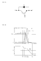
FIG. 1a is a schematic view illustrating symbols used in IGBT, where D refers to a diode, C refers to a collector, E refers to an emitter and G refers to a gate. -
FIG, 1b is a graph illustrating a characteristic of turn-off at the IGBT. If a gate voltage surpasses a threshold voltage based on a gate electrostatic capacity, the IGBT is turned on, and turned off if the gate voltage goes down below the threshold voltage. - A collector-emitter voltage (VCE) generated during switching of IGBT is generated by transient voltage caused by stray inductance on a conductive line and input voltage. Thus, there is needed an IGBT driving technology capable of limiting a transient voltage level.
-
FIG.2 is a schematic view illustrating an IGBT driving method according to prior art. - Referring to
FIG.2 , a transient voltage Vce is generated across an IGBT in a parallel circuit where aconventional IGBT 100 and passive elements R, L andC 200 are connected in parallel during turn-off operation of a current flowing to theIGBT 100. The transient voltage has an absolute influence to damage ofIGBT 100. -
Snubber circuits 300 are connected in parallel to prevent the transient voltage in the conventional IGBT circuit. The term of snubber refers to an auxiliary circuit element or combination of elements used for alleviating the transient voltage in a semiconductor device. The snubber circuit is largely formed with an RC (Resistor-Capacitor) or an RCD (Resistor-Capacitor-Diode). However, thesnubber circuit 300 needs much more number of passive power elements during high voltage design, such that the passive elements cause a problem of generating an additional loss during IGBT operation. - The present disclosure has been made to solve the foregoing problem(s) of the prior art, and therefore an object of certain embodiments of the present invention is to provide a method for driving an IGBT configured to control a slope of a gate-emitter voltage that is an IGBT control signal.
- In one general aspect of the present disclosure, there is provided a method for driving an IGBT configured to reduce a transient voltage applied across the IGBT during turn-off of an IGBT driver IC (Integrated Circuit), the method comprising: reducing a slope of a gate-emitter voltage of the IGBT to reduce the transient voltage across the IGBT.
- Preferably, but not necessarily, the step of reducing a slope of a gate-emitter voltage of the IGBT is performed by changing an inner resistance of the IGBT driver IC.
- Preferably, but not necessarily, the inner resistance of the IGBT driver IC is changed to substantially 25kΩ
- Preferably, but not necessarily, the step of reducing a slope of a gate-emitter voltage of the IGBT is performed by lengthening a holding time of a threshold voltage of IGBT.
- The method for driving IGBT according to the present disclosure has an advantageous effect in that a voltage applied across the IGBT during the current cut-off can be efficiently reduced by controlling a slope of a gate-emitter voltage that is an IGBT control signal and by reducing a slope of a current during current cut-off of IGBT.
- The drawing figures depict one or more exemplary embodiments in accord with the present concepts, by way of example only, not by way of limitations. In the figures, like reference numerals refer to the same or similar elements.
- Thus, a wide variety of potential practical and useful embodiments will be more readily understood through the following detailed description of certain exemplary embodiments, with reference to the accompanying exemplary drawings in which:
-
FIG. 1a is a schematic view illustrating symbols used in IGBT; -
FIG.1b is a graph illustrating a characteristic of turn-off at the IGBT; -
FIG.2 is a schematic view illustrating an IGBT driving method according to prior art; -
FIG.3 is a schematic view illustrating a method for driving an IGBT according to an exemplary embodiment of the present disclosure; -
FIG.4a is a graph illustrating changed slopes of VGE according to an exemplary embodiment of the present disclosure; and -
FIG.4b is a graph illustrating a voltage across the IGBT ofFIG.4a . - The disclosed embodiments and advantages thereof are best understood by referring to
FIGS. 1-4 of the drawings, like numerals being used for like and corresponding parts of the various drawings. Other features and advantages of the disclosed embodiments will be or will become apparent to one of ordinary skill in the art upon examination of the following figures and detailed description. It is intended that all such additional features and advantages be included within the scope of the disclosed embodiments, and protected by the accompanying drawings. Further, the illustrated figures are only exemplary and not intended to assert or imply any limitation with regard to the environment, architecture, or process in which different embodiments may be implemented. Accordingly, the described aspect is intended to embrace all such alterations, modifications, and variations that fall within the scope and novel idea of the present invention. - Meanwhile, the terminology used herein is for the purpose of describing particular implementations only and is not intended to be limiting of the present disclosure. The terms "first," "second," and the like, herein do not denote any order, quantity, or importance, but rather are used to distinguish one element from another. For example, a second constituent element may be denoted as a first constituent element without departing from the scope and spirit of the present disclosure, and similarly, a first constituent element may be denoted as a second constituent element.
- As used herein, the terms "a" and "an" herein do not denote a limitation of quantity, but rather denote the presence of at least one of the referenced item. That is, as used herein, the singular forms "a", "an" and "the" are intended to include the plural forms as well, unless the context clearly indicates otherwise.
- It will be understood that when an element is referred to as being "connected" or "coupled" to another element, it can be directly connected or coupled to the other element or intervening elements may be present. In contrast, when an element is referred to as being "directly connected" or "directly coupled" to another element, there are no intervening elements present.
- It will be further understood that the terms "comprises" and/or "comprising," or "includes" and/or "including" when used in this specification, specify the presence of stated features, regions, integers, steps, operations, elements, and/or components, but do not preclude the presence or addition of one or more other features, regions, integers, steps, operations, elements, components, and/or groups thereof.
- Also, "exemplary" is merely meant to mean an example, rather than the best. If is also to be appreciated that features, layers and/or elements depicted herein are illustrated with particular dimensions and/or orientations relative to one another for purposes of simplicity and ease of understanding, and that the actual dimensions and/or orientations may differ substantially from that illustrated.
- That is, in the drawings, the size and relative sizes of layers, regions and/or other elements may be exaggerated or reduced for clarity. Like numbers refer to like elements throughout and explanations that duplicate one another will be omitted. As may be used herein, the terms "substantially" and "approximately" provide an industry-accepted tolerance for its corresponding term and/or relativity between items.
- Hereinafter, a method for driving IGBT according to the present disclosure will be described in detail with reference to the accompanying drawings.
- The present disclosure proposes a method for changing a VGE characteristic for controlling an IGBT current, in order to remove a snubber circuit (300) of
FIG.2 and to reduce a transient voltage across an IGBT during IGBT current cut-off operation. That is, the present disclosure uses an IGBT switching technology, instead of forming a snubber circuit, to prevent the IGBT from being damaged by the transient voltage. -
FIG.3 is a schematic view illustrating a method for driving an IGBT according to an exemplary embodiment of the present disclosure. - Referring to
FIG.3 , the IGBT driving according to the present disclosure is performed by an IGBT driver IC (not shown). That is, although not shown, the IGBT driving according to the present disclosure is performed by an IC (Integrated Circuit) connected to the IGBT. - As shown in the figure, an IGBT driving circuit is formed in parallel with an
IGBT 10 and apassive element 20 including a resistor (R), an inductor (L) and a capacitor (C), and the IGBT driving IC (not shown) is configured to transmit a control signal to theIGBT 10. - A transient voltage (Vce) across the
IGBT 10 or a peak voltage during turn-off operation of theIGBT 10 is determined by Ldi/dt, where L refers to an inductance of the inductor included in the parallel-connectedpassive element 20, and di/dt refers to a slope of a current during the turn-off operation. - That is, either the inductance L is reduced or the slope of turned-off current is reduced to reduce the transient voltage. However, reducing the inductance L is limited due to circuit configuration, such that it would be more effective to reduce the slope of the current.
- Therefore, the present disclosure proposes a method of changing a slope of VGE which is a control signal of IGBT in order to reduce the turned-off current. That is, a level of current conducted on the IGBT is changed in response to a value of VGE which is a control signal of IGBT, such that the slope of current during the IGBT turn-off operation can be reduced by control of VGE
-
FIG.4a is a graph illustrating changed slopes of VGE according to an exemplary embodiment of the present disclosure, andFIG.4b is a graph illustrating a voltage across the IGBT ofFIG.4a . - Referring to
FIGS. 4a and 4b , the method for driving the IGBT according to an exemplary embodiment of the present disclosure is to change the slope of VGE, as a method for changing an inner resistance of the IGBT driver IC (not shown). - That is, it can be noted from
FIG. 4a that the slope of VGE is reduced when an inner resistance of the IGBT driver IC is 25kΩ instead of 5kΩ, where it can be noted that a voltage (VIGBT) across the IGBT is also reduced. - As noted above, the method for driving IGBT is to reduce the voltage across the IGBT by reducing the slope of VGE through increased inner resistance of the IGBT driver IC.
- However, it should be apparent that the method of reducing the slope of VGE is not limited to the increased inner resistance of the IGBT driver IC, but can be done by lengthening a holding time of a threshold voltage, for example.
- The method for driving the IGBT proposes a method of reducing a slope of VGE, which is a gate-emitter control signal of IGBT inputted from the IGBT driver IC, in order to reduce a slope of turned-off current. The level of current conductive to the IBGT is changed by the value of VGE, which is an IGBT control signal, where the slope of current during IGBT turn-off operation can be reduced by control of VGE.
- The method for driving IGBT according to the present disclosure has an industrial applicability in that a voltage applied across the IGBT during the current cut-off can be efficiently reduced by controlling a slope of a gate-emitter voltage that is an IGBT control signal and by reducing a slope of a current during current cut-off of IGBT.
- Although the present disclosure has been described with reference to a number of illustrative embodiments thereof, it should be understood that numerous other modifications and embodiments can be devised by those skilled in the art that will fall within the spirit and scope of the principles of this disclosure.
- More particularly, various variations and modifications are possible in the component parts and/or arrangements of subject combination arrangement within the scope of the disclosure, the drawings and the appended claims. In addition to variations and modifications in the component parts and/or arrangements, alternative uses will also be apparent to those skilled in the art.
Claims (4)
- A method for driving an IGBT (10) configured to reduce a transient voltage applied across the IGBT (10) during turn-off of an IGBT driver IC (Integrated Circuit), the method comprising: reducing a slope of a gate-emitter voltage of the IGBT to reduce the transient voltage across the IGBT.
- The method of claim 1, wherein the step of reducing a slope of a gate-emitter voltage of the IGBT (10) is performed by changing an inner resistance of the IGBT driver IC.
- The method of claim 1 or 2, wherein the inner resistance of the IGBT driver IC is changed to substantially 25kΩ.
- The method of any one of claims 1, 2 and 3, wherein the step of reducing a slope of a gate-emitter voltage of the IGBT (10) is performed by lengthening a holding time of a threshold voltage of IGBT (10).
Applications Claiming Priority (1)
| Application Number | Priority Date | Filing Date | Title |
|---|---|---|---|
| KR1020110073229A KR20130011812A (en) | 2011-07-22 | 2011-07-22 | Method for driving igbt |
Publications (1)
| Publication Number | Publication Date |
|---|---|
| EP2549650A1 true EP2549650A1 (en) | 2013-01-23 |
Family
ID=46785217
Family Applications (1)
| Application Number | Title | Priority Date | Filing Date |
|---|---|---|---|
| EP12173744A Withdrawn EP2549650A1 (en) | 2011-07-22 | 2012-06-27 | Method for driving IGBT |
Country Status (5)
| Country | Link |
|---|---|
| US (1) | US8723591B2 (en) |
| EP (1) | EP2549650A1 (en) |
| JP (1) | JP2013027307A (en) |
| KR (1) | KR20130011812A (en) |
| CN (1) | CN102891669A (en) |
Families Citing this family (33)
| Publication number | Priority date | Publication date | Assignee | Title |
|---|---|---|---|---|
| US10587257B2 (en) | 2013-04-04 | 2020-03-10 | Tm4 Inc. | Commutation cell and compensation circuit therefor |
| US9655221B2 (en) | 2013-08-19 | 2017-05-16 | Eagle Harbor Technologies, Inc. | High frequency, repetitive, compact toroid-generation for radiation production |
| US10020800B2 (en) | 2013-11-14 | 2018-07-10 | Eagle Harbor Technologies, Inc. | High voltage nanosecond pulser with variable pulse width and pulse repetition frequency |
| US9706630B2 (en) | 2014-02-28 | 2017-07-11 | Eagle Harbor Technologies, Inc. | Galvanically isolated output variable pulse generator disclosure |
| US10978955B2 (en) | 2014-02-28 | 2021-04-13 | Eagle Harbor Technologies, Inc. | Nanosecond pulser bias compensation |
| US10892140B2 (en) | 2018-07-27 | 2021-01-12 | Eagle Harbor Technologies, Inc. | Nanosecond pulser bias compensation |
| US11539352B2 (en) | 2013-11-14 | 2022-12-27 | Eagle Harbor Technologies, Inc. | Transformer resonant converter |
| CN109873621B (en) | 2013-11-14 | 2023-06-16 | 鹰港科技有限公司 | High-voltage nanosecond pulse generator |
| US9444448B2 (en) | 2013-12-10 | 2016-09-13 | General Electric Company | High performance IGBT gate drive |
| US10790816B2 (en) * | 2014-01-27 | 2020-09-29 | Eagle Harbor Technologies, Inc. | Solid-state replacement for tube-based modulators |
| US10483089B2 (en) | 2014-02-28 | 2019-11-19 | Eagle Harbor Technologies, Inc. | High voltage resistive output stage circuit |
| US9496864B2 (en) | 2014-12-18 | 2016-11-15 | General Electric Company | Gate drive circuit and method of operating same |
| US11542927B2 (en) | 2015-05-04 | 2023-01-03 | Eagle Harbor Technologies, Inc. | Low pressure dielectric barrier discharge plasma thruster |
| US9812941B2 (en) | 2015-09-11 | 2017-11-07 | Nxp Usa, Inc. | High power driver having multiple turn off modes |
| CN105790743A (en) * | 2016-04-13 | 2016-07-20 | 中国人民解放军国防科学技术大学 | Active source voltage control large power IGBT method and system |
| US11430635B2 (en) | 2018-07-27 | 2022-08-30 | Eagle Harbor Technologies, Inc. | Precise plasma control system |
| US10903047B2 (en) | 2018-07-27 | 2021-01-26 | Eagle Harbor Technologies, Inc. | Precise plasma control system |
| US11004660B2 (en) | 2018-11-30 | 2021-05-11 | Eagle Harbor Technologies, Inc. | Variable output impedance RF generator |
| EP4266579A3 (en) | 2017-02-07 | 2023-12-27 | Eagle Harbor Technologies, Inc. | Transformer resonant converter |
| EP3665775B1 (en) | 2017-08-25 | 2025-08-20 | Eagle Harbor Technologies, Inc. | Arbitrary waveform generation using nanosecond pulses |
| US11222767B2 (en) | 2018-07-27 | 2022-01-11 | Eagle Harbor Technologies, Inc. | Nanosecond pulser bias compensation |
| US10607814B2 (en) | 2018-08-10 | 2020-03-31 | Eagle Harbor Technologies, Inc. | High voltage switch with isolated power |
| US11532457B2 (en) | 2018-07-27 | 2022-12-20 | Eagle Harbor Technologies, Inc. | Precise plasma control system |
| US11302518B2 (en) | 2018-07-27 | 2022-04-12 | Eagle Harbor Technologies, Inc. | Efficient energy recovery in a nanosecond pulser circuit |
| US11810761B2 (en) | 2018-07-27 | 2023-11-07 | Eagle Harbor Technologies, Inc. | Nanosecond pulser ADC system |
| KR102499709B1 (en) | 2018-08-10 | 2023-02-16 | 이글 하버 테크놀로지스, 인코포레이티드 | Plasma sheath control for RF plasma reactors |
| US12456604B2 (en) | 2019-12-24 | 2025-10-28 | Eagle Harbor Technologies, Inc. | Nanosecond pulser RF isolation for plasma systems |
| KR20240028538A (en) | 2019-01-08 | 2024-03-05 | 이글 하버 테크놀로지스, 인코포레이티드 | Efficient energy recovery in a nanosecond pulser circuit |
| TWI778449B (en) | 2019-11-15 | 2022-09-21 | 美商鷹港科技股份有限公司 | High voltage pulsing circuit |
| KR20230150396A (en) | 2019-12-24 | 2023-10-30 | 이글 하버 테크놀로지스, 인코포레이티드 | Nanosecond pulser rf isolation for plasma systems |
| US11967484B2 (en) | 2020-07-09 | 2024-04-23 | Eagle Harbor Technologies, Inc. | Ion current droop compensation |
| US11824542B1 (en) | 2022-06-29 | 2023-11-21 | Eagle Harbor Technologies, Inc. | Bipolar high voltage pulser |
| CN119998919A (en) | 2022-09-29 | 2025-05-13 | 鹰港科技有限公司 | High pressure plasma control |
Citations (4)
| Publication number | Priority date | Publication date | Assignee | Title |
|---|---|---|---|---|
| US6333665B1 (en) * | 1999-02-26 | 2001-12-25 | Kabushiki Kaisha Toshiba | Gate circuit for insulated gate semiconductor device |
| US20020070772A1 (en) * | 2000-10-23 | 2002-06-13 | International Rectifier Corporation | Gate drive circuit with feedback-controlled active resistance |
| US20040196678A1 (en) * | 2003-04-03 | 2004-10-07 | Mitsubishi Denki Kabushiki Kaisha | Power conversion apparatus and power conversion system having the power conversion apparatus |
| GB2433358A (en) * | 2005-12-13 | 2007-06-20 | Bombardier Transp Gmbh | Operating electronic valves having an insulated gate |
Family Cites Families (14)
| Publication number | Priority date | Publication date | Assignee | Title |
|---|---|---|---|---|
| US5444591A (en) * | 1993-04-01 | 1995-08-22 | International Rectifier Corporation | IGBT fault current limiting circuit |
| JP3373704B2 (en) | 1995-08-25 | 2003-02-04 | 三菱電機株式会社 | Insulated gate transistor drive circuit |
| JP3421507B2 (en) * | 1996-07-05 | 2003-06-30 | 三菱電機株式会社 | Driver circuit for semiconductor device |
| JP3161589B2 (en) * | 1996-10-17 | 2001-04-25 | 富士電機株式会社 | Power converter gate drive circuit |
| JP4846106B2 (en) * | 2001-02-16 | 2011-12-28 | 三菱電機株式会社 | Field effect semiconductor device and method for manufacturing the same |
| JP2007288094A (en) * | 2006-04-20 | 2007-11-01 | Fuji Electric Device Technology Co Ltd | IGBT and gate drive circuit for driving the same |
| JP2008306618A (en) * | 2007-06-11 | 2008-12-18 | Nissan Motor Co Ltd | Driving circuit for driving a voltage driven element |
| JP2009071956A (en) * | 2007-09-12 | 2009-04-02 | Mitsubishi Electric Corp | Gate drive circuit |
| US7570101B1 (en) * | 2008-02-27 | 2009-08-04 | The United States Of America As Represented By The United States Department Of Energy | Advanced insulated gate bipolar transistor gate drive |
| KR100967781B1 (en) | 2008-04-10 | 2010-07-05 | 엘에스산전 주식회사 | Drive circuit of switching element in inverter |
| KR101449083B1 (en) * | 2010-05-06 | 2014-10-13 | 엘에스산전 주식회사 | Switching Gate Drive |
| JP5460519B2 (en) * | 2010-08-09 | 2014-04-02 | 本田技研工業株式会社 | Semiconductor device driving apparatus and method |
| CN102097418B (en) * | 2010-12-17 | 2012-06-27 | 中国北车股份有限公司大连电力牵引研发中心 | IGBT driving unit |
| US8400739B2 (en) * | 2011-02-28 | 2013-03-19 | General Electric Company | System and method for operating inverters |
-
2011
- 2011-07-22 KR KR1020110073229A patent/KR20130011812A/en not_active Ceased
-
2012
- 2012-06-21 US US13/530,008 patent/US8723591B2/en active Active
- 2012-06-27 EP EP12173744A patent/EP2549650A1/en not_active Withdrawn
- 2012-07-19 CN CN2012102520251A patent/CN102891669A/en active Pending
- 2012-07-20 JP JP2012161511A patent/JP2013027307A/en active Pending
Patent Citations (4)
| Publication number | Priority date | Publication date | Assignee | Title |
|---|---|---|---|---|
| US6333665B1 (en) * | 1999-02-26 | 2001-12-25 | Kabushiki Kaisha Toshiba | Gate circuit for insulated gate semiconductor device |
| US20020070772A1 (en) * | 2000-10-23 | 2002-06-13 | International Rectifier Corporation | Gate drive circuit with feedback-controlled active resistance |
| US20040196678A1 (en) * | 2003-04-03 | 2004-10-07 | Mitsubishi Denki Kabushiki Kaisha | Power conversion apparatus and power conversion system having the power conversion apparatus |
| GB2433358A (en) * | 2005-12-13 | 2007-06-20 | Bombardier Transp Gmbh | Operating electronic valves having an insulated gate |
Also Published As
| Publication number | Publication date |
|---|---|
| US8723591B2 (en) | 2014-05-13 |
| KR20130011812A (en) | 2013-01-30 |
| US20130021067A1 (en) | 2013-01-24 |
| JP2013027307A (en) | 2013-02-04 |
| CN102891669A (en) | 2013-01-23 |
Similar Documents
| Publication | Publication Date | Title |
|---|---|---|
| US8723591B2 (en) | Method for driving IGBT | |
| JP5783997B2 (en) | Power semiconductor device | |
| US10396651B2 (en) | Power conversion apparatus | |
| JP5452549B2 (en) | Power module | |
| US11539361B2 (en) | Semiconductor device signal transmission circuit for drive-control, method of controlling semiconductor device signal transmission circuit for drive-control, semiconductor device, power conversion device, and electric system for railway vehicle | |
| CN104604134A (en) | Semiconductor apparatus | |
| JP5925364B2 (en) | Power semiconductor device | |
| JP2016059036A (en) | Circuit, system and method for short circuit protection | |
| JP2009071956A (en) | Gate drive circuit | |
| CN104426333B (en) | Driving circuit and semiconductor device | |
| JP5348912B2 (en) | Semiconductor device drive circuit | |
| KR101329610B1 (en) | Semiconductor device | |
| US20120256493A1 (en) | Switching device and switching module | |
| JP2012034079A (en) | Driving circuit for insulated gate type device | |
| Crisafulli et al. | Kelvin Source connection for High Current IGBTs. A way to get high energy efficiency | |
| JP5630484B2 (en) | Semiconductor device | |
| JP4110052B2 (en) | Inverter circuit | |
| US20230412167A1 (en) | Power Electronic Module Comprising a Gate-Source Control Unit | |
| JP5832845B2 (en) | Semiconductor module and power conversion module | |
| JP6627351B2 (en) | Switching circuit device | |
| JP4830829B2 (en) | Insulated gate transistor drive circuit | |
| JP6312946B1 (en) | Power semiconductor element drive circuit and motor drive device | |
| CN113647019A (en) | Circuit arrangement for a semiconductor switch | |
| CN107534015A (en) | Protection circuit and protection circuit system | |
| WO2015079875A1 (en) | Semiconductor device |
Legal Events
| Date | Code | Title | Description |
|---|---|---|---|
| PUAI | Public reference made under article 153(3) epc to a published international application that has entered the european phase |
Free format text: ORIGINAL CODE: 0009012 |
|
| AK | Designated contracting states |
Kind code of ref document: A1 Designated state(s): AL AT BE BG CH CY CZ DE DK EE ES FI FR GB GR HR HU IE IS IT LI LT LU LV MC MK MT NL NO PL PT RO RS SE SI SK SM TR |
|
| AX | Request for extension of the european patent |
Extension state: BA ME |
|
| 17P | Request for examination filed |
Effective date: 20130723 |
|
| RBV | Designated contracting states (corrected) |
Designated state(s): AL AT BE BG CH CY CZ DE DK EE ES FI FR GB GR HR HU IE IS IT LI LT LU LV MC MK MT NL NO PL PT RO RS SE SI SK SM TR |
|
| 17Q | First examination report despatched |
Effective date: 20161215 |
|
| STAA | Information on the status of an ep patent application or granted ep patent |
Free format text: STATUS: THE APPLICATION IS DEEMED TO BE WITHDRAWN |
|
| 18D | Application deemed to be withdrawn |
Effective date: 20170426 |