EP2547484B1 - Kondensator-leiterplatten-schnittstelle zum schweissen von systemkomponenten - Google Patents
Kondensator-leiterplatten-schnittstelle zum schweissen von systemkomponenten Download PDFInfo
- Publication number
- EP2547484B1 EP2547484B1 EP11731060.7A EP11731060A EP2547484B1 EP 2547484 B1 EP2547484 B1 EP 2547484B1 EP 11731060 A EP11731060 A EP 11731060A EP 2547484 B1 EP2547484 B1 EP 2547484B1
- Authority
- EP
- European Patent Office
- Prior art keywords
- circuit board
- capacitor
- welding system
- interface
- terminal
- Prior art date
- Legal status (The legal status is an assumption and is not a legal conclusion. Google has not performed a legal analysis and makes no representation as to the accuracy of the status listed.)
- Not-in-force
Links
Images




Classifications
-
- H—ELECTRICITY
- H05—ELECTRIC TECHNIQUES NOT OTHERWISE PROVIDED FOR
- H05K—PRINTED CIRCUITS; CASINGS OR CONSTRUCTIONAL DETAILS OF ELECTRIC APPARATUS; MANUFACTURE OF ASSEMBLAGES OF ELECTRICAL COMPONENTS
- H05K3/00—Apparatus or processes for manufacturing printed circuits
- H05K3/30—Assembling printed circuits with electric components, e.g. with resistors
- H05K3/32—Assembling printed circuits with electric components, e.g. with resistors electrically connecting electric components or wires to printed circuits
-
- B—PERFORMING OPERATIONS; TRANSPORTING
- B23—MACHINE TOOLS; METAL-WORKING NOT OTHERWISE PROVIDED FOR
- B23K—SOLDERING OR UNSOLDERING; WELDING; CLADDING OR PLATING BY SOLDERING OR WELDING; CUTTING BY APPLYING HEAT LOCALLY, e.g. FLAME CUTTING; WORKING BY LASER BEAM
- B23K9/00—Arc welding or cutting
- B23K9/10—Other electric circuits therefor; Protective circuits; Remote controls
-
- Y—GENERAL TAGGING OF NEW TECHNOLOGICAL DEVELOPMENTS; GENERAL TAGGING OF CROSS-SECTIONAL TECHNOLOGIES SPANNING OVER SEVERAL SECTIONS OF THE IPC; TECHNICAL SUBJECTS COVERED BY FORMER USPC CROSS-REFERENCE ART COLLECTIONS [XRACs] AND DIGESTS
- Y10—TECHNICAL SUBJECTS COVERED BY FORMER USPC
- Y10T—TECHNICAL SUBJECTS COVERED BY FORMER US CLASSIFICATION
- Y10T29/00—Metal working
- Y10T29/49—Method of mechanical manufacture
- Y10T29/49002—Electrical device making
-
- Y—GENERAL TAGGING OF NEW TECHNOLOGICAL DEVELOPMENTS; GENERAL TAGGING OF CROSS-SECTIONAL TECHNOLOGIES SPANNING OVER SEVERAL SECTIONS OF THE IPC; TECHNICAL SUBJECTS COVERED BY FORMER USPC CROSS-REFERENCE ART COLLECTIONS [XRACs] AND DIGESTS
- Y10—TECHNICAL SUBJECTS COVERED BY FORMER USPC
- Y10T—TECHNICAL SUBJECTS COVERED BY FORMER US CLASSIFICATION
- Y10T29/00—Metal working
- Y10T29/49—Method of mechanical manufacture
- Y10T29/49002—Electrical device making
- Y10T29/49117—Conductor or circuit manufacturing
-
- Y—GENERAL TAGGING OF NEW TECHNOLOGICAL DEVELOPMENTS; GENERAL TAGGING OF CROSS-SECTIONAL TECHNOLOGIES SPANNING OVER SEVERAL SECTIONS OF THE IPC; TECHNICAL SUBJECTS COVERED BY FORMER USPC CROSS-REFERENCE ART COLLECTIONS [XRACs] AND DIGESTS
- Y10—TECHNICAL SUBJECTS COVERED BY FORMER USPC
- Y10T—TECHNICAL SUBJECTS COVERED BY FORMER US CLASSIFICATION
- Y10T29/00—Metal working
- Y10T29/49—Method of mechanical manufacture
- Y10T29/49002—Electrical device making
- Y10T29/49117—Conductor or circuit manufacturing
- Y10T29/49124—On flat or curved insulated base, e.g., printed circuit, etc.
-
- Y—GENERAL TAGGING OF NEW TECHNOLOGICAL DEVELOPMENTS; GENERAL TAGGING OF CROSS-SECTIONAL TECHNOLOGIES SPANNING OVER SEVERAL SECTIONS OF THE IPC; TECHNICAL SUBJECTS COVERED BY FORMER USPC CROSS-REFERENCE ART COLLECTIONS [XRACs] AND DIGESTS
- Y10—TECHNICAL SUBJECTS COVERED BY FORMER USPC
- Y10T—TECHNICAL SUBJECTS COVERED BY FORMER US CLASSIFICATION
- Y10T29/00—Metal working
- Y10T29/49—Method of mechanical manufacture
- Y10T29/49002—Electrical device making
- Y10T29/49117—Conductor or circuit manufacturing
- Y10T29/49124—On flat or curved insulated base, e.g., printed circuit, etc.
- Y10T29/4913—Assembling to base an electrical component, e.g., capacitor, etc.
-
- Y—GENERAL TAGGING OF NEW TECHNOLOGICAL DEVELOPMENTS; GENERAL TAGGING OF CROSS-SECTIONAL TECHNOLOGIES SPANNING OVER SEVERAL SECTIONS OF THE IPC; TECHNICAL SUBJECTS COVERED BY FORMER USPC CROSS-REFERENCE ART COLLECTIONS [XRACs] AND DIGESTS
- Y10—TECHNICAL SUBJECTS COVERED BY FORMER USPC
- Y10T—TECHNICAL SUBJECTS COVERED BY FORMER US CLASSIFICATION
- Y10T29/00—Metal working
- Y10T29/49—Method of mechanical manufacture
- Y10T29/49002—Electrical device making
- Y10T29/49117—Conductor or circuit manufacturing
- Y10T29/49124—On flat or curved insulated base, e.g., printed circuit, etc.
- Y10T29/4913—Assembling to base an electrical component, e.g., capacitor, etc.
- Y10T29/49133—Assembling to base an electrical component, e.g., capacitor, etc. with component orienting
-
- Y—GENERAL TAGGING OF NEW TECHNOLOGICAL DEVELOPMENTS; GENERAL TAGGING OF CROSS-SECTIONAL TECHNOLOGIES SPANNING OVER SEVERAL SECTIONS OF THE IPC; TECHNICAL SUBJECTS COVERED BY FORMER USPC CROSS-REFERENCE ART COLLECTIONS [XRACs] AND DIGESTS
- Y10—TECHNICAL SUBJECTS COVERED BY FORMER USPC
- Y10T—TECHNICAL SUBJECTS COVERED BY FORMER US CLASSIFICATION
- Y10T29/00—Metal working
- Y10T29/49—Method of mechanical manufacture
- Y10T29/49002—Electrical device making
- Y10T29/49117—Conductor or circuit manufacturing
- Y10T29/49194—Assembling elongated conductors, e.g., splicing, etc.
- Y10T29/49195—Assembling elongated conductors, e.g., splicing, etc. with end-to-end orienting
- Y10T29/49199—Assembling elongated conductors, e.g., splicing, etc. with end-to-end orienting including deforming of joining bridge
Definitions
- the present disclosure relates to welding system components, and more specifically, to an interface between a capacitor and circuit board for a component of a welding system.
- Welding is an important process in the manufacture and construction of various products and structures. Applications for welding are widespread and used throughout the world including, for example, the construction and repair of ships, buildings, bridges, vehicles, and pipe lines, to name a few. Welding is performed in a variety of locations, such as in a factory with a fixed welding operation or on site with a portable welder.
- a user/operator i.e. welder
- programs or instructs welding equipment to make a weld For example, in Submerged Arc Welding (SAW) a consumable solid or tubular (flux cored) electrode may be continuously fed into a molten weld or arc zone that is protected from atmospheric contamination by being "submerged” under flux such as a blanket of granular fusible material consisting of lime, silica, manganese oxide, calcium fluoride, or other suitable compounds. Generally, when molten, the flux becomes conductive, and provides a current path between the electrode and the work.
- SAW Submerged Arc Welding
- a thick layer of flux completely covering the molten metal may thus prevent spatter and sparks as well as suppress the intense ultraviolet radiation and fumes that may be a part of the arc welding process.
- currents ranging from 300 to 2000 A may be utilized. Additionally, currents of up to 5000 A may be used with multiple arcs.
- DC or AC power can be used, and/or combinations of DC and AC in multiple electrode systems.
- constant voltage welding power supplies are most commonly used; however, constant current systems in combination with a voltage sensing wire-feeder are also available.
- a user/operator i.e. welder
- welder directs welding equipment to make a weld.
- the welder may manually position a welding rod or welding wire and produce a heat generating arc at a weld location.
- the spacing of the electrode from the weld location is related to the arc produced and to the achievement of optimum melting/fusing of the base and welding rod or wire metals. The quality of such a weld is often directly dependant upon the skill of the welder.
- Submerged Arc Welding and Electric Arc Welding may occur in a variety of environments. As such, it is generally desirable to protect the components of welding systems for use in a variety of conditions.
- connections of capacitors to circuit boards are typically high temperature connections due to the nature of the materials of capacitors. This heat is typically displaced into the circuit board and thus raises the temperature of the board and other components mounted to the board. It is desired to minimize this heat transfer from the capacitor connections to the board.
- EP -A1- 1 669 152 discloses a welding system component comprising a circuit board, a capacitor and an interface for mounting the capacitor to the circuit board.
- This invention provides a welding system component according to claim 1 and a method of assembling a welding system component according to claim 11. Further embodiments of the invention are comprised in the dependent claims.
- a welding system component includes a circuit board for the welding system component.
- An interface has a main riser portion with a fastener passageway formed therethrough.
- the interface has an extension portion with a terminal passageway formed therethrough.
- the extension portion is electrically connected to the circuit board with a terminal disposed in the terminal passageway.
- the extension portion is spaced away from a surface of the circuit board.
- a capacitor is electrically connected to the main riser portion with a fastener disposed in the fastener passageway.
- Fig. 1 is a schematic view of a welding environment
- Fig. 2 is a perspective view of the welder of Fig. 1 ;
- Fig. 3 is an enlarged view of a portion of the welder of Fig. 2 shown with the access panel shown partially cut away;
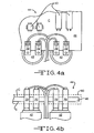
- Fig. 4a is a top view of a portion of the circuit board assembly shown in Fig. 3 ;
- Fig. 4b is a front view of the portion of the circuit board assembly shown in Fig. 4a ;
- Fig. 5 is an enlarged side view of a portion of the circuit board assembly of Fig 4b ;
- Fig. 6 is a perspective view of the interface of Fig. 5 ;
- Fig. 7 is a top view of the interface of Fig. 6 ;
- Fig. 8 is a side view of the interface of Fig. 6 ;
- Fig. 9 is a front view of the interface of Fig. 6 .
- Welding environment 10 includes welding system 12, and work piece 14.
- Welding system 12 includes welding gun 16 with a wire feed passage connected to a wire feeder (not shown) and with an electrode connected to welding power supply 18.
- Exemplary welding environment 10 also includes wire feed controller 20 and power controller 22 with user interface 24 for programming and monitoring system 12.
- welding environment may also, for example, include a stick electrode holder, TIG torch or other apparatus for use with electric arc welding or other equipment as appropriate for other types of welding.
- Work piece 14 and proximate space generally defines welding work area 26 where the welding gun may be used to form a weld.
- Various types of exemplary welding including Submerged Arc Welding (SAW), Shielded Metal Arc Welding (SMAW), Gas Metal Arc Welding (GMAW) e.g. MIG melding, and Gas Tungsten Arc Welding (GTAW) e.g. TIG welding, may be conducted in the welding environment.
- SAW Submerged Arc Welding
- SMAW Shielded Metal Arc Welding
- GMAW Gas Metal Arc Welding
- GTAW Gas Tungsten Arc Welding
- Welding system 12 includes welding equipment, such as welding power supply 18, for generating a welding current and voltage, a welding control system for controlling the welding current and voltage, and a monitoring system for monitoring the welding current and voltage.
- the monitoring system may also monitor a variety of other operating parameters, such as but not limited to, welding wire feed speed, amount of welding wire remaining, any type of welding feedback desired by the operator, and any other desired operating parameters.
- welding power supply 18 is illustrated for line powered welding, e.g. welding supplied with electric power from a power grid. However it must be understood that welding power supply 18 may be for other types of welding, such as engine welding, e.g. with a motor-generator.
- Welding power supply 18 includes cabinet 28 that is suitable to house equipment that supplies power to output leads for welding.
- Cabinet 28 includes base 30, an access panel 32, control panel 34, side panels 36 and cover 38.
- Access panel 32 may include optional air louvers. Access panel 32 may provide access to an optional fan(s), such as an impeller or blower disposed in cabinet 28.
- an optional fan(s) such as an impeller or blower disposed in cabinet 28.
- Welding power supply 18 or user interface may optionally include a number of input devices, such as a knob, slides, switches, buttons or other digital or analog controls , for example to adjust the output of the welder or perform other control operations, e.g. welding mode, arc control, etc, and may be mounted on control panel 34. Additionally, display devices may also fastened to welding power supply 18 or user interface for display of operation parameters of welding system 12, as well as optional gauges.
- the input devices may be associated with a control board with or without an optional chopper.
- welding power supply 18 also includes various electronic components 40 as desired, such as switches, resistors, rectifiers, diodes, power control boards, and capacitors 42. As desired, a variety of these components maybe mounted within a compartment in cabinet 28 adjacent control panel 34. As such, in the illustrated example, they are accessible through a front opening associated with control panel 34.
- Circuit board assembly 44 for association with capacitors 42 is shown in Figs. 4a and 4b .
- Circuit board assembly 44 includes circuit board 46 that has solder side "S" and component side C.
- Circuit board assembly 44 may optionally include a number of associated electrical components 40 electrically connected to circuit board 46.
- an optional heat sink assembly (not shown) may be thermally connected to circuit board 46.
- capacitor 42 is connected to circuit board 46 by at least one interface 70.
- Circuit board assembly 44 includes a pair of mounting terminals (one shown); positive mounting terminal 72 and a negative mounting terminal (not shown) each connected to respective interface 70.
- Figs. 5-9 are described with regard to positive mounting terminal 72. It must be understood however, that the connection to an arrangement of the negative mounting terminal (not shown) and respective interface 70 a similar to that of positive mounting terminal 72 as described below, except as otherwise noted.
- interface 70 includes main riser portion 74 and an extension portion 76 which generally extends a distance in a direction that is substantially normal to the longitudinal direction of main riser portion 74, although such is not required.
- Exemplary interface 70 is machined from a single piece of copper. However, it must be understood that interface 70 may be formed from any other suitable material, such as copper alloy, aluminum, aluminum alloy or any other material suitable to support capacitor 42 and form an electrically conductive path between circuit board 46 and capacitor 42.
- Interface 70 may act as a heat sink and reduce heat from circuit board 46 and/or capacitor 42. This tends to protect circuit board 46 and allow components 40 connected there to run cooler, as compared to when capacitor 42 is connected directly to circuit board 46. As a result, a plurality of capacitors 42 may be bussed together, as illustrated in Figs. 4a and 4b , and/or be placed closer together on circuit board 46 than otherwise would be the case. Additionally, this configuration minimizes inductance in during the setup of circuit board assembly 44. It is noted that in at least one configuration circuit board 46 may include a thick copper substrate upon which other layers and components are placed.
- Main riser portion 74 includes fastener passageway 78 formed there through.
- Extension portion 76 extends from one end of main riser portion 74 and includes terminal passageway 80 formed there through.
- Fastener passageway 78 is formed such that fastener 82, such as a bolt or other fastening device, may be disposed therein to fasten interface 70 to capacitor 42, either directly or with an optional component mount 84, which, for example, may be made of a different material than interface 70.
- Interface 70 may optionally be fastened to capacitor 42 by clips, screws, pins or any other mechanism suitable to electrically connect interface 70 to capacitor 42.
- fastener 82 provides an optional first positive lead connection 86 such that one or more leads may be mounted to the top of interface 70 to electrically connect to board 46 and/or capacitor 42. Additionally or alternatively an optional washer may be disposed between the end of fastener 82 and the surface of interface 70.
- Terminal passageway 80 is formed such that terminal 72 may be disposed therein to mount circuit board 46 to interface 70 and electrically connect capacitor 42 to circuit board 46.
- Terminal 72 may be fastened to interface 70 by a bolt, clip, screw, pin or any other mechanism suitable to electrically connect circuit board 46 to interface 70.
- the connection to terminal 72 may provide an optional second positive lead connection 88 such that one or more leads may be mounted to the top of interface 70 to electrically connect to circuit board 46 and/or capacitor 42.
- interface 70 associated with the negative mounting terminal may also have similar first and second negative lead connections such that one or more leads may be mounted to the top of interface 70 associated with the negative mounting terminal (not shown) to electrically connect to board 46 and/or capacitor 42.
- an optional washer may be disposed between the end of terminal 72 and the surface of interface 70.
- terminal 72 may be connected to component side "C" of circuit board 46, along with any desired components 40.
- main riser portion 74 extends away from the surface of circuit board 46 with extension portion 76 being elevated off the surface of circuit board 46.
- main riser portion 74 extends generally orthogonally to the surface of circuit board 46 with extension portion 76 extending generally parallel to the surface of circuit board 46.
- Circuit board 46 may optionally be covered with encapsulation material 90. Subsequently, capacitor 42 and interface 70 may then be connected to circuit board 46.
- portions of the circuit board 46 may be dammed as desired, circuit board 46 covered with encapsulation material 90 and terminal 72 and other components 66 then connected, with capacitor 42 and interface 70.
- terminal 72, and thus interface 70 may be mounted on solder side "S" of circuit board 46 such that capacitor 42 may be positioned on solder side Sand thus allow a connection to be made to component side "C" at a minimal distance.
- main riser portion 74 extends away from the surface of circuit board 46 with extension portion 76 being elevated off the surface of circuit board 46.
- main riser portion 74 extends generally orthogonally to the surface of circuit board 46 with extension portion 76 extending generally parallel to the surface of circuit board 46.
- connections to terminal 72 may be made with greater force than the connections to fastener 82.
- fastener 82 may be tightened with 10 to 15 inch-pounds of torque, while the terminal may be tightened with 50 inch-pounds of torque or more.
- interface 70 may reduce unwanted heat from being absorbed circuit board 46 during assembly.
- Main riser portion 74 and extension portion 76 disrupt the heat from capacitor 42 from being absorbed into circuit board 46.
- the plurality of interfaces 70 may be mounted relatively closely together during assembly.
Landscapes
- Engineering & Computer Science (AREA)
- Physics & Mathematics (AREA)
- Plasma & Fusion (AREA)
- Mechanical Engineering (AREA)
- Manufacturing & Machinery (AREA)
- Microelectronics & Electronic Packaging (AREA)
- Inverter Devices (AREA)
- Generation Of Surge Voltage And Current (AREA)
- Electric Connection Of Electric Components To Printed Circuits (AREA)
- Arc Welding Control (AREA)
Claims (15)
- Schweißsystemkomponente, die Folgendes umfasst:eine Leiterplatte (46) für eine Schweißsystemkomponente,einen Kondensator (42),eine Schnittstelle (70) zum Montieren des Kondensators (42) an der Leiterplatte (46), und ein Mittel zum elektrischen Verbinden des Kondensators (42) mit der Leiterplatte (46),dadurch gekennzeichnet, dassdie Schnittstelle (70) einen aufstrebenden Hauptabschnitt (74), durch den hindurch ein Befestigungsmitteldurchgang (78) verläuft, und einen Verlängerungsabschnitt (76), durch den hindurch ein Anschlussdurchgang (80) verläuft, enthält.
- Schweißsystemkomponente nach Anspruch 1, die des Weiteren ein Mittel zum Schützen der Leiterplatte umfasst, das die Leiterplatte (46) mindestens teilweise bedeckt, und/oder wobei das Mittel zum elektrischen Verbinden des Kondensators mit der Leiterplatte (46) ein Mittel zum Verbinden einer Anschlussleitung enthält.
- Schweißsystemkomponente nach Anspruch 1 oder 2, die des Weiteren erste und zweite Anschlüsse umfasst, die mit der Leiterplatte verbunden sind, und wobei das Mittel zum elektrischen Verbinden des Kondensators mit der Leiterplatte ein erstes Mittel zum elektrischen Verbinden des Kondensators mit der Leiterplatte ist, das mit dem ersten Anschluss verbunden ist, und wobei das Schweißsystem ein zweites Mittel zum elektrischen Verbinden des Kondensators mit der Leiterplatte enthält, das mit dem zweiten Anschluss verbunden ist.
- Schweißsystemkomponente nach einem der Ansprüche 1 bis 3, wobei der Verlängerungsabschnitt (76) elektrisch mit der Leiterplatte (46) verbunden ist, wobei ein Anschluss (72) in dem Anschlussdurchgang (80) angeordnet ist und der Verlängerungsabschnitt (76) von einer Oberfläche der Leiterplatte (46) beabstandet ist, und wobei der mindestens eine Kondensator (42) elektrisch mit dem aufstrebenden Hauptabschnitt (74) verbunden ist, wobei ein Befestigungsmittel in dem Befestigungsmittel (82)-durchgang (78) angeordnet ist.
- Schweißsystemkomponente nach einem der Ansprüche 1 bis 4, wobei die Leiterplatte (46) mindestens teilweise mit einem Verkapselungsmaterial bedeckt ist.
- Schweißsystemkomponente nach einem der Ansprüche 1 bis 5, wobei sich der aufstrebende Hauptabschnitt (74) allgemein orthogonal zur Oberfläche der Leiterplatte (46) erstreckt, und/oder wobei sich der Verlängerungsabschnitt (76) allgemein parallel zur Oberfläche der Leiterplatte (46) erstreckt.
- Schweißsystemkomponente nach einem der Ansprüche 1 bis 6, die des Weiteren eine zweite Schnittstelle umfasst, die einen aufstrebenden Hauptabschnitt, durch den hindurch ein Befestigungsmitteldurchgang verläuft, und einen Verlängerungsabschnitt, durch den hindurch ein Anschlussdurchgang verläuft, enthält, wobei der aufstrebende Hauptabschnitt elektrisch mit dem Kondensator verbunden ist, wobei ein Befestigungsmittel in dem Befestigungsmitteldurchgang angeordnet ist und der Verlängerungsabschnitt von einer Oberfläche der Leiterplatte beabstandet ist, und wobei die Leiterplatte elektrisch mit dem Verlängerungsabschnitt der zweiten Schnittstelle verbunden ist, wobei ein zweiter Anschluss in dem Anschlussdurchgang der zweiten Schnittstelle angeordnet ist.
- Schweißsystemkomponente nach einem der Ansprüche 1 bis 7, wobei der Stromfluss durch den Anschluss zwischen dem Verlängerungsabschnitt und der Leiterplatte stattfindet.
- Schweißsystemkomponente nach einem der Ansprüche 1 bis 8, wobei der Kondensator ein erster Kondensator ist, und die des Weiteren einen zweiten Kondensator umfasst, der elektrisch mit der Leiterplatte verbunden ist und über eine Sammelschiene mit dem ersten Kondensator verbunden ist.
- Schweißsystemkomponente nach einem der Ansprüche 1 bis 9, wobei das Befestigungsmittel eine Anschlussleitungsverbindung bereitstellt und/oder wobei der Anschluss eine Anschlussleitungsverbindung bereitstellt.
- Verfahren zum Montieren einer Schweißsystemkomponente, das Folgendes umfasst:(a) Bereitstellen einer Leiterplatte (46) für eine Schweißsystemkomponente;(b) Bereitstellen mindestens eines Kondensators (42),
gekennzeichnet durch(c) Bereitstellen einer Schnittstelle (70), die einen aufstrebenden Hauptabschnitt (74), durch den hindurch ein Befestigungsmitteldurchgang (78) verläuft, und einen Verlängerungsabschnitt (76), durch den hindurch ein Anschlussdurchgang (80) verläuft, enthält,(d) elektrisches Verbinden des aufstrebenden Hauptabschnitts (74) mit dem mindestens einen Kondensator (42), wobei ein Befestigungsmittel (82) in dem Befestigungsmitteldurchgang (78) angeordnet ist;(e) elektrisches Verbinden der Leiterplatte (46) mit dem Verlängerungsabschnitt (76), wobei ein Anschluss (72) dergestalt in dem Anschlussdurchgang (80) angeordnet ist, dass der Verlängerungsabschnitt (76) von einer Oberfläche der Leiterplatte (46) beabstandet ist. - Verfahren zum Montieren einer Schweißsystemkomponente nach Anspruch 11, das des Weiteren folgenden Schritt umfasst:(f) mindestens teilweises Bedecken der Leiterplatte mit einem Verkapselungsmaterial.
- Verfahren zum Montieren einer Schweißsystemkomponente nach Anspruch 12, wobei der Schritt des Bedeckens (f) vor dem Verbinden in Schritt (e) ausgeführt wird.
- Verfahren zum Montieren einer Schweißsystemkomponente nach einem der Ansprüche 11 bis 13, das des Weiteren folgende Schritte umfasst:(g) Bereitstellen einer zweiten Schnittstelle, die einen aufstrebenden Hauptabschnitt, durch den hindurch ein Befestigungsmitteldurchgang verläuft, und einen Verlängerungsabschnitt, durch den hindurch ein Anschlussdurchgang verläuft, enthält,(h) elektrisches Verbinden des aufstrebenden Hauptabschnitts der zweiten Schnittstelle mit dem Kondensator, wobei ein zweites Befestigungsmittel in dem Befestigungsmitteldurchgang der zweiten Schnittstelle angeordnet ist, und(i) elektrisches Verbinden der Leiterplatte mit dem Verlängerungsabschnitt der zweiten Schnittstelle, wobei ein zweiter Anschluss dergestalt in dem Anschlussdurchgang der zweiten Schnittstelle angeordnet ist, dass der Verlängerungsabschnitt der zweiten Schnittstelle von einer Oberfläche der Leiterplatte beabstandet ist.
- Verfahren zum Montieren einer Schweißsystemkomponente nach einem der Ansprüche 11 bis 14, wobei der Kondensator ein erster Kondensator ist, und das des Weiteren folgende Schritte umfasst:(j) Bereitstellen eines zweiten Kondensators,(k) elektrisches Verbinden des zweiten Kondensators mit der Leiterplatte, und(l) Verbinden des zweiten Kondensators über eine Sammelschiene mit dem ersten Kondensator.
Priority Applications (1)
| Application Number | Priority Date | Filing Date | Title |
|---|---|---|---|
| PL11731060T PL2547484T3 (pl) | 2010-03-15 | 2011-03-15 | Złącze kondensator – płytka drukowana dla komponentów systemu spawalniczego |
Applications Claiming Priority (2)
| Application Number | Priority Date | Filing Date | Title |
|---|---|---|---|
| US12/724,075 US8604355B2 (en) | 2010-03-15 | 2010-03-15 | Capacitor-circuit board interface for welding system components |
| PCT/IB2011/000546 WO2011114216A1 (en) | 2010-03-15 | 2011-03-15 | Capacitor-circuit board interface for welding system components |
Publications (2)
| Publication Number | Publication Date |
|---|---|
| EP2547484A1 EP2547484A1 (de) | 2013-01-23 |
| EP2547484B1 true EP2547484B1 (de) | 2013-08-21 |
Family
ID=44317731
Family Applications (1)
| Application Number | Title | Priority Date | Filing Date |
|---|---|---|---|
| EP11731060.7A Not-in-force EP2547484B1 (de) | 2010-03-15 | 2011-03-15 | Kondensator-leiterplatten-schnittstelle zum schweissen von systemkomponenten |
Country Status (9)
| Country | Link |
|---|---|
| US (2) | US8604355B2 (de) |
| EP (1) | EP2547484B1 (de) |
| JP (1) | JP5566479B2 (de) |
| CN (1) | CN102791416A (de) |
| BR (1) | BR112012019466A2 (de) |
| CA (1) | CA2785091A1 (de) |
| MX (1) | MX2012010525A (de) |
| PL (1) | PL2547484T3 (de) |
| WO (1) | WO2011114216A1 (de) |
Families Citing this family (1)
| Publication number | Priority date | Publication date | Assignee | Title |
|---|---|---|---|---|
| US8604355B2 (en) * | 2010-03-15 | 2013-12-10 | Lincoln Global, Inc. | Capacitor-circuit board interface for welding system components |
Family Cites Families (23)
| Publication number | Priority date | Publication date | Assignee | Title |
|---|---|---|---|---|
| US3200296A (en) * | 1962-10-26 | 1965-08-10 | Rca Corp | Combined mounting-bracket and heat-sink |
| US3681664A (en) * | 1971-08-19 | 1972-08-01 | Jfd Electronics Corp | Trimmer capacitor for printed circuit board |
| US3790860A (en) * | 1972-07-17 | 1974-02-05 | Trygen Electronics Inc | Power supply chassis assembly for electronic circuit with cooling |
| JPS633129U (de) * | 1986-06-23 | 1988-01-11 | ||
| JPH01189991A (ja) | 1988-01-26 | 1989-07-31 | Nec Corp | プリント配線板への部品実装方法 |
| JPH0340894U (de) * | 1989-08-30 | 1991-04-19 | ||
| US5420745A (en) * | 1991-09-30 | 1995-05-30 | Matsushita Electric Industrial Co., Ltd. | Surface-mount type ceramic capacitor |
| US5214564A (en) * | 1992-04-23 | 1993-05-25 | Sunstrand Corporation | Capacitor assembly with integral cooling apparatus |
| US5747773A (en) * | 1995-12-18 | 1998-05-05 | The Esab Group, Inc. | Arc welder power source |
| US5760361A (en) * | 1996-05-24 | 1998-06-02 | Square D Company | Multiple single phase weld control systems from a polyphase power source |
| DE19953594A1 (de) * | 1998-11-20 | 2000-05-25 | Matsushita Electric Industrial Co Ltd | Oberflächenmontierte elektronische Komponente |
| WO2000055875A1 (en) * | 1999-03-16 | 2000-09-21 | Maxwell Energy Products | Low inductance four terminal capacitor lead frame |
| US6418029B1 (en) * | 2000-02-28 | 2002-07-09 | Mckee James S. | Interconnect system having vertically mounted passive components on an underside of a substrate |
| JP3589174B2 (ja) * | 2000-10-24 | 2004-11-17 | 株式会社村田製作所 | 表面実装型正特性サーミスタおよびその実装方法 |
| US6532157B1 (en) * | 2000-11-16 | 2003-03-11 | Amkor Technology, Inc. | Angulated semiconductor packages |
| JP2005050962A (ja) * | 2003-07-31 | 2005-02-24 | Taiyo Yuden Co Ltd | コンデンサ実装構造,コンデンサ実装基板及びコンデンサ実装用配線基板 |
| US8530789B2 (en) * | 2004-12-13 | 2013-09-10 | Lincoln Global, Inc. | Power module cartridge |
| CN101611493A (zh) | 2006-12-19 | 2009-12-23 | 泰瑟拉互连材料公司 | 嵌有片状电容器的印刷电路板 |
| US20090111294A1 (en) * | 2007-10-25 | 2009-04-30 | Gm Global Technology Operations, Inc. | Bus bar to printed circuit board interface for electric and hybrid electric vehicles |
| US8373084B2 (en) * | 2007-12-19 | 2013-02-12 | Illinois Tool Works Inc. | Plasma cutter having high power density |
| IL190329A (en) * | 2008-03-20 | 2014-11-30 | Celem Passive Components Ltd | Get high-powered cooled by side-by-side transmission |
| JP4634498B2 (ja) * | 2008-11-28 | 2011-02-16 | 三菱電機株式会社 | 電力用半導体モジュール |
| US8604355B2 (en) * | 2010-03-15 | 2013-12-10 | Lincoln Global, Inc. | Capacitor-circuit board interface for welding system components |
-
2010
- 2010-03-15 US US12/724,075 patent/US8604355B2/en not_active Expired - Fee Related
-
2011
- 2011-03-15 JP JP2012554444A patent/JP5566479B2/ja not_active Expired - Fee Related
- 2011-03-15 CN CN2011800140603A patent/CN102791416A/zh active Pending
- 2011-03-15 EP EP11731060.7A patent/EP2547484B1/de not_active Not-in-force
- 2011-03-15 PL PL11731060T patent/PL2547484T3/pl unknown
- 2011-03-15 BR BR112012019466A patent/BR112012019466A2/pt not_active IP Right Cessation
- 2011-03-15 CA CA2785091A patent/CA2785091A1/en not_active Abandoned
- 2011-03-15 MX MX2012010525A patent/MX2012010525A/es not_active Application Discontinuation
- 2011-03-15 WO PCT/IB2011/000546 patent/WO2011114216A1/en not_active Ceased
-
2013
- 2013-03-07 US US13/788,348 patent/US8898894B2/en not_active Expired - Fee Related
Also Published As
| Publication number | Publication date |
|---|---|
| AU2011228803A1 (en) | 2012-07-05 |
| CN102791416A (zh) | 2012-11-21 |
| BR112012019466A2 (pt) | 2016-05-03 |
| US8604355B2 (en) | 2013-12-10 |
| WO2011114216A1 (en) | 2011-09-22 |
| US8898894B2 (en) | 2014-12-02 |
| EP2547484A1 (de) | 2013-01-23 |
| JP5566479B2 (ja) | 2014-08-06 |
| PL2547484T3 (pl) | 2014-04-30 |
| JP2013520322A (ja) | 2013-06-06 |
| CA2785091A1 (en) | 2011-09-22 |
| US20110220400A1 (en) | 2011-09-15 |
| US20130185933A1 (en) | 2013-07-25 |
| MX2012010525A (es) | 2012-10-15 |
Similar Documents
| Publication | Publication Date | Title |
|---|---|---|
| EP2707168B1 (de) | Lichtbogenschweisssystem und -verfahren mit flussmittelseele und hoher abscheidungsrate sowie verschweissung mit robuster schlagzähigkeit | |
| Weman | Welding processes handbook | |
| US8476555B2 (en) | Portable welding wire feed system and method | |
| CA2797724C (en) | Welding system comprising an induction heating system, induction heating system and method of heating a welding or cutting work piece | |
| EP3634680B1 (de) | Vorheizstromversorgung zur steuerung des stroms | |
| CA2651219C (en) | Welding device with arc termination control | |
| US20080023457A1 (en) | Method and Apparatus For Pulse and Short Circuit Arc Welding | |
| US8080762B2 (en) | Electric arc welding machine with control interface | |
| MXPA06002546A (es) | Soldador con alimentador integrado de alambre que tiene control por medio de una sola perilla. | |
| US20120211472A1 (en) | Welding system with rotational speed converter for auxiliary power generator | |
| US8898894B2 (en) | Capacitor-circuit board interface for welding system components | |
| AU2011228803B2 (en) | Capacitor-circuit board interface for welding system components | |
| MX2015000182A (es) | Inductor y sistema para soldar para mantener arcos de soldadura. | |
| US12280450B2 (en) | Integrated compressed air cooling for welding systems | |
| CA3123927C (en) | Integrated compressed air cooling for welding systems | |
| Sindhu et al. | The study on effect of process parameters on weld deposits in pulsed gas metal arc welding | |
| KR200236717Y1 (ko) | 전극집게가 구비된 휴대용 용접기 | |
| CA3288575A1 (en) | Floating universal torch fume capture attachment | |
| KR20230103548A (ko) | 하이브리드 용접기 | |
| Allgood | Power Sources for Arc Welding |
Legal Events
| Date | Code | Title | Description |
|---|---|---|---|
| PUAI | Public reference made under article 153(3) epc to a published international application that has entered the european phase |
Free format text: ORIGINAL CODE: 0009012 |
|
| 17P | Request for examination filed |
Effective date: 20120917 |
|
| AK | Designated contracting states |
Kind code of ref document: A1 Designated state(s): AL AT BE BG CH CY CZ DE DK EE ES FI FR GB GR HR HU IE IS IT LI LT LU LV MC MK MT NL NO PL PT RO RS SE SI SK SM TR |
|
| GRAP | Despatch of communication of intention to grant a patent |
Free format text: ORIGINAL CODE: EPIDOSNIGR1 |
|
| DAX | Request for extension of the european patent (deleted) | ||
| GRAS | Grant fee paid |
Free format text: ORIGINAL CODE: EPIDOSNIGR3 |
|
| GRAA | (expected) grant |
Free format text: ORIGINAL CODE: 0009210 |
|
| AK | Designated contracting states |
Kind code of ref document: B1 Designated state(s): AL AT BE BG CH CY CZ DE DK EE ES FI FR GB GR HR HU IE IS IT LI LT LU LV MC MK MT NL NO PL PT RO RS SE SI SK SM TR |
|
| REG | Reference to a national code |
Ref country code: GB Ref legal event code: FG4D |
|
| REG | Reference to a national code |
Ref country code: CH Ref legal event code: EP |
|
| REG | Reference to a national code |
Ref country code: AT Ref legal event code: REF Ref document number: 627766 Country of ref document: AT Kind code of ref document: T Effective date: 20130915 |
|
| REG | Reference to a national code |
Ref country code: IE Ref legal event code: FG4D |
|
| REG | Reference to a national code |
Ref country code: DE Ref legal event code: R096 Ref document number: 602011002715 Country of ref document: DE Effective date: 20131017 |
|
| REG | Reference to a national code |
Ref country code: SE Ref legal event code: TRGR |
|
| REG | Reference to a national code |
Ref country code: NL Ref legal event code: VDEP Effective date: 20130821 |
|
| REG | Reference to a national code |
Ref country code: LT Ref legal event code: MG4D |
|
| PG25 | Lapsed in a contracting state [announced via postgrant information from national office to epo] |
Ref country code: NO Free format text: LAPSE BECAUSE OF FAILURE TO SUBMIT A TRANSLATION OF THE DESCRIPTION OR TO PAY THE FEE WITHIN THE PRESCRIBED TIME-LIMIT Effective date: 20131121 Ref country code: PT Free format text: LAPSE BECAUSE OF FAILURE TO SUBMIT A TRANSLATION OF THE DESCRIPTION OR TO PAY THE FEE WITHIN THE PRESCRIBED TIME-LIMIT Effective date: 20131223 Ref country code: HR Free format text: LAPSE BECAUSE OF FAILURE TO SUBMIT A TRANSLATION OF THE DESCRIPTION OR TO PAY THE FEE WITHIN THE PRESCRIBED TIME-LIMIT Effective date: 20130821 Ref country code: CY Free format text: LAPSE BECAUSE OF FAILURE TO SUBMIT A TRANSLATION OF THE DESCRIPTION OR TO PAY THE FEE WITHIN THE PRESCRIBED TIME-LIMIT Effective date: 20130918 Ref country code: LT Free format text: LAPSE BECAUSE OF FAILURE TO SUBMIT A TRANSLATION OF THE DESCRIPTION OR TO PAY THE FEE WITHIN THE PRESCRIBED TIME-LIMIT Effective date: 20130821 Ref country code: IS Free format text: LAPSE BECAUSE OF FAILURE TO SUBMIT A TRANSLATION OF THE DESCRIPTION OR TO PAY THE FEE WITHIN THE PRESCRIBED TIME-LIMIT Effective date: 20131221 |
|
| PG25 | Lapsed in a contracting state [announced via postgrant information from national office to epo] |
Ref country code: LV Free format text: LAPSE BECAUSE OF FAILURE TO SUBMIT A TRANSLATION OF THE DESCRIPTION OR TO PAY THE FEE WITHIN THE PRESCRIBED TIME-LIMIT Effective date: 20130821 Ref country code: FI Free format text: LAPSE BECAUSE OF FAILURE TO SUBMIT A TRANSLATION OF THE DESCRIPTION OR TO PAY THE FEE WITHIN THE PRESCRIBED TIME-LIMIT Effective date: 20130821 Ref country code: BE Free format text: LAPSE BECAUSE OF FAILURE TO SUBMIT A TRANSLATION OF THE DESCRIPTION OR TO PAY THE FEE WITHIN THE PRESCRIBED TIME-LIMIT Effective date: 20130821 Ref country code: GR Free format text: LAPSE BECAUSE OF FAILURE TO SUBMIT A TRANSLATION OF THE DESCRIPTION OR TO PAY THE FEE WITHIN THE PRESCRIBED TIME-LIMIT Effective date: 20131122 |
|
| PG25 | Lapsed in a contracting state [announced via postgrant information from national office to epo] |
Ref country code: CY Free format text: LAPSE BECAUSE OF FAILURE TO SUBMIT A TRANSLATION OF THE DESCRIPTION OR TO PAY THE FEE WITHIN THE PRESCRIBED TIME-LIMIT Effective date: 20130821 |
|
| PG25 | Lapsed in a contracting state [announced via postgrant information from national office to epo] |
Ref country code: EE Free format text: LAPSE BECAUSE OF FAILURE TO SUBMIT A TRANSLATION OF THE DESCRIPTION OR TO PAY THE FEE WITHIN THE PRESCRIBED TIME-LIMIT Effective date: 20130821 Ref country code: RO Free format text: LAPSE BECAUSE OF FAILURE TO SUBMIT A TRANSLATION OF THE DESCRIPTION OR TO PAY THE FEE WITHIN THE PRESCRIBED TIME-LIMIT Effective date: 20130821 Ref country code: DK Free format text: LAPSE BECAUSE OF FAILURE TO SUBMIT A TRANSLATION OF THE DESCRIPTION OR TO PAY THE FEE WITHIN THE PRESCRIBED TIME-LIMIT Effective date: 20130821 Ref country code: NL Free format text: LAPSE BECAUSE OF FAILURE TO SUBMIT A TRANSLATION OF THE DESCRIPTION OR TO PAY THE FEE WITHIN THE PRESCRIBED TIME-LIMIT Effective date: 20130821 Ref country code: SK Free format text: LAPSE BECAUSE OF FAILURE TO SUBMIT A TRANSLATION OF THE DESCRIPTION OR TO PAY THE FEE WITHIN THE PRESCRIBED TIME-LIMIT Effective date: 20130821 Ref country code: CZ Free format text: LAPSE BECAUSE OF FAILURE TO SUBMIT A TRANSLATION OF THE DESCRIPTION OR TO PAY THE FEE WITHIN THE PRESCRIBED TIME-LIMIT Effective date: 20130821 |
|
| PGFP | Annual fee paid to national office [announced via postgrant information from national office to epo] |
Ref country code: SE Payment date: 20140327 Year of fee payment: 4 |
|
| REG | Reference to a national code |
Ref country code: PL Ref legal event code: T3 |
|
| PG25 | Lapsed in a contracting state [announced via postgrant information from national office to epo] |
Ref country code: ES Free format text: LAPSE BECAUSE OF FAILURE TO SUBMIT A TRANSLATION OF THE DESCRIPTION OR TO PAY THE FEE WITHIN THE PRESCRIBED TIME-LIMIT Effective date: 20130821 |
|
| PGFP | Annual fee paid to national office [announced via postgrant information from national office to epo] |
Ref country code: PL Payment date: 20140219 Year of fee payment: 4 Ref country code: FR Payment date: 20140317 Year of fee payment: 4 Ref country code: IT Payment date: 20140331 Year of fee payment: 4 |
|
| PLBE | No opposition filed within time limit |
Free format text: ORIGINAL CODE: 0009261 |
|
| STAA | Information on the status of an ep patent application or granted ep patent |
Free format text: STATUS: NO OPPOSITION FILED WITHIN TIME LIMIT |
|
| 26N | No opposition filed |
Effective date: 20140522 |
|
| PGFP | Annual fee paid to national office [announced via postgrant information from national office to epo] |
Ref country code: DE Payment date: 20140327 Year of fee payment: 4 |
|
| REG | Reference to a national code |
Ref country code: DE Ref legal event code: R097 Ref document number: 602011002715 Country of ref document: DE Effective date: 20140522 |
|
| PG25 | Lapsed in a contracting state [announced via postgrant information from national office to epo] |
Ref country code: LU Free format text: LAPSE BECAUSE OF FAILURE TO SUBMIT A TRANSLATION OF THE DESCRIPTION OR TO PAY THE FEE WITHIN THE PRESCRIBED TIME-LIMIT Effective date: 20140315 |
|
| REG | Reference to a national code |
Ref country code: CH Ref legal event code: PL |
|
| REG | Reference to a national code |
Ref country code: IE Ref legal event code: MM4A |
|
| PG25 | Lapsed in a contracting state [announced via postgrant information from national office to epo] |
Ref country code: CH Free format text: LAPSE BECAUSE OF NON-PAYMENT OF DUE FEES Effective date: 20140331 Ref country code: IE Free format text: LAPSE BECAUSE OF NON-PAYMENT OF DUE FEES Effective date: 20140315 Ref country code: LI Free format text: LAPSE BECAUSE OF NON-PAYMENT OF DUE FEES Effective date: 20140331 |
|
| REG | Reference to a national code |
Ref country code: DE Ref legal event code: R119 Ref document number: 602011002715 Country of ref document: DE |
|
| GBPC | Gb: european patent ceased through non-payment of renewal fee |
Effective date: 20150315 |
|
| PG25 | Lapsed in a contracting state [announced via postgrant information from national office to epo] |
Ref country code: SE Free format text: LAPSE BECAUSE OF NON-PAYMENT OF DUE FEES Effective date: 20150316 |
|
| REG | Reference to a national code |
Ref country code: SE Ref legal event code: EUG |
|
| PG25 | Lapsed in a contracting state [announced via postgrant information from national office to epo] |
Ref country code: IT Free format text: LAPSE BECAUSE OF NON-PAYMENT OF DUE FEES Effective date: 20150315 |
|
| REG | Reference to a national code |
Ref country code: FR Ref legal event code: ST Effective date: 20151130 |
|
| PG25 | Lapsed in a contracting state [announced via postgrant information from national office to epo] |
Ref country code: GB Free format text: LAPSE BECAUSE OF NON-PAYMENT OF DUE FEES Effective date: 20150315 Ref country code: DE Free format text: LAPSE BECAUSE OF NON-PAYMENT OF DUE FEES Effective date: 20151001 |
|
| PG25 | Lapsed in a contracting state [announced via postgrant information from national office to epo] |
Ref country code: FR Free format text: LAPSE BECAUSE OF NON-PAYMENT OF DUE FEES Effective date: 20150331 Ref country code: MT Free format text: LAPSE BECAUSE OF FAILURE TO SUBMIT A TRANSLATION OF THE DESCRIPTION OR TO PAY THE FEE WITHIN THE PRESCRIBED TIME-LIMIT Effective date: 20130821 |
|
| PG25 | Lapsed in a contracting state [announced via postgrant information from national office to epo] |
Ref country code: SM Free format text: LAPSE BECAUSE OF FAILURE TO SUBMIT A TRANSLATION OF THE DESCRIPTION OR TO PAY THE FEE WITHIN THE PRESCRIBED TIME-LIMIT Effective date: 20130821 |
|
| PG25 | Lapsed in a contracting state [announced via postgrant information from national office to epo] |
Ref country code: PL Free format text: LAPSE BECAUSE OF NON-PAYMENT OF DUE FEES Effective date: 20150315 Ref country code: MC Free format text: LAPSE BECAUSE OF FAILURE TO SUBMIT A TRANSLATION OF THE DESCRIPTION OR TO PAY THE FEE WITHIN THE PRESCRIBED TIME-LIMIT Effective date: 20130821 |
|
| PG25 | Lapsed in a contracting state [announced via postgrant information from national office to epo] |
Ref country code: RS Free format text: LAPSE BECAUSE OF FAILURE TO SUBMIT A TRANSLATION OF THE DESCRIPTION OR TO PAY THE FEE WITHIN THE PRESCRIBED TIME-LIMIT Effective date: 20130821 Ref country code: BG Free format text: LAPSE BECAUSE OF FAILURE TO SUBMIT A TRANSLATION OF THE DESCRIPTION OR TO PAY THE FEE WITHIN THE PRESCRIBED TIME-LIMIT Effective date: 20130821 |
|
| PG25 | Lapsed in a contracting state [announced via postgrant information from national office to epo] |
Ref country code: TR Free format text: LAPSE BECAUSE OF FAILURE TO SUBMIT A TRANSLATION OF THE DESCRIPTION OR TO PAY THE FEE WITHIN THE PRESCRIBED TIME-LIMIT Effective date: 20130821 Ref country code: SI Free format text: LAPSE BECAUSE OF FAILURE TO SUBMIT A TRANSLATION OF THE DESCRIPTION OR TO PAY THE FEE WITHIN THE PRESCRIBED TIME-LIMIT Effective date: 20130821 Ref country code: HU Free format text: LAPSE BECAUSE OF FAILURE TO SUBMIT A TRANSLATION OF THE DESCRIPTION OR TO PAY THE FEE WITHIN THE PRESCRIBED TIME-LIMIT; INVALID AB INITIO Effective date: 20110315 |
|
| REG | Reference to a national code |
Ref country code: AT Ref legal event code: MM01 Ref document number: 627766 Country of ref document: AT Kind code of ref document: T Effective date: 20160315 |
|
| PG25 | Lapsed in a contracting state [announced via postgrant information from national office to epo] |
Ref country code: AT Free format text: LAPSE BECAUSE OF NON-PAYMENT OF DUE FEES Effective date: 20160315 |
|
| PG25 | Lapsed in a contracting state [announced via postgrant information from national office to epo] |
Ref country code: MK Free format text: LAPSE BECAUSE OF FAILURE TO SUBMIT A TRANSLATION OF THE DESCRIPTION OR TO PAY THE FEE WITHIN THE PRESCRIBED TIME-LIMIT Effective date: 20130821 |
|
| PG25 | Lapsed in a contracting state [announced via postgrant information from national office to epo] |
Ref country code: AL Free format text: LAPSE BECAUSE OF FAILURE TO SUBMIT A TRANSLATION OF THE DESCRIPTION OR TO PAY THE FEE WITHIN THE PRESCRIBED TIME-LIMIT Effective date: 20130821 |