EP2546870A2 - Metal-bonded ceramic substrate - Google Patents
Metal-bonded ceramic substrate Download PDFInfo
- Publication number
- EP2546870A2 EP2546870A2 EP11753594A EP11753594A EP2546870A2 EP 2546870 A2 EP2546870 A2 EP 2546870A2 EP 11753594 A EP11753594 A EP 11753594A EP 11753594 A EP11753594 A EP 11753594A EP 2546870 A2 EP2546870 A2 EP 2546870A2
- Authority
- EP
- European Patent Office
- Prior art keywords
- ceramic substrate
- metal
- metal layer
- bonding
- cutting line
- Prior art date
- Legal status (The legal status is an assumption and is not a legal conclusion. Google has not performed a legal analysis and makes no representation as to the accuracy of the status listed.)
- Withdrawn
Links
Images


Classifications
-
- H—ELECTRICITY
- H10—SEMICONDUCTOR DEVICES; ELECTRIC SOLID-STATE DEVICES NOT OTHERWISE PROVIDED FOR
- H10W—GENERIC PACKAGES, INTERCONNECTIONS, CONNECTORS OR OTHER CONSTRUCTIONAL DETAILS OF DEVICES COVERED BY CLASS H10
- H10W40/00—Arrangements for thermal protection or thermal control
- H10W40/20—Arrangements for cooling
- H10W40/25—Arrangements for cooling characterised by their materials
- H10W40/255—Arrangements for cooling characterised by their materials having a laminate or multilayered structure, e.g. direct bond copper [DBC] ceramic substrates
-
- C—CHEMISTRY; METALLURGY
- C04—CEMENTS; CONCRETE; ARTIFICIAL STONE; CERAMICS; REFRACTORIES
- C04B—LIME, MAGNESIA; SLAG; CEMENTS; COMPOSITIONS THEREOF, e.g. MORTARS, CONCRETE OR LIKE BUILDING MATERIALS; ARTIFICIAL STONE; CERAMICS; REFRACTORIES; TREATMENT OF NATURAL STONE
- C04B37/00—Joining burned ceramic articles with other burned ceramic articles or other articles by heating
- C04B37/02—Joining burned ceramic articles with other burned ceramic articles or other articles by heating with metallic articles
- C04B37/023—Joining burned ceramic articles with other burned ceramic articles or other articles by heating with metallic articles characterised by the interlayer used
- C04B37/026—Joining burned ceramic articles with other burned ceramic articles or other articles by heating with metallic articles characterised by the interlayer used consisting of metals or metal salts
-
- H—ELECTRICITY
- H10—SEMICONDUCTOR DEVICES; ELECTRIC SOLID-STATE DEVICES NOT OTHERWISE PROVIDED FOR
- H10W—GENERIC PACKAGES, INTERCONNECTIONS, CONNECTORS OR OTHER CONSTRUCTIONAL DETAILS OF DEVICES COVERED BY CLASS H10
- H10W70/00—Package substrates; Interposers; Redistribution layers [RDL]
- H10W70/60—Insulating or insulated package substrates; Interposers; Redistribution layers
- H10W70/67—Insulating or insulated package substrates; Interposers; Redistribution layers characterised by their insulating layers or insulating parts
- H10W70/69—Insulating materials thereof
- H10W70/692—Ceramics or glasses
-
- C—CHEMISTRY; METALLURGY
- C04—CEMENTS; CONCRETE; ARTIFICIAL STONE; CERAMICS; REFRACTORIES
- C04B—LIME, MAGNESIA; SLAG; CEMENTS; COMPOSITIONS THEREOF, e.g. MORTARS, CONCRETE OR LIKE BUILDING MATERIALS; ARTIFICIAL STONE; CERAMICS; REFRACTORIES; TREATMENT OF NATURAL STONE
- C04B2237/00—Aspects relating to ceramic laminates or to joining of ceramic articles with other articles by heating
- C04B2237/30—Composition of layers of ceramic laminates or of ceramic or metallic articles to be joined by heating, e.g. Si substrates
- C04B2237/32—Ceramic
- C04B2237/34—Oxidic
- C04B2237/343—Alumina or aluminates
-
- C—CHEMISTRY; METALLURGY
- C04—CEMENTS; CONCRETE; ARTIFICIAL STONE; CERAMICS; REFRACTORIES
- C04B—LIME, MAGNESIA; SLAG; CEMENTS; COMPOSITIONS THEREOF, e.g. MORTARS, CONCRETE OR LIKE BUILDING MATERIALS; ARTIFICIAL STONE; CERAMICS; REFRACTORIES; TREATMENT OF NATURAL STONE
- C04B2237/00—Aspects relating to ceramic laminates or to joining of ceramic articles with other articles by heating
- C04B2237/30—Composition of layers of ceramic laminates or of ceramic or metallic articles to be joined by heating, e.g. Si substrates
- C04B2237/32—Ceramic
- C04B2237/36—Non-oxidic
- C04B2237/365—Silicon carbide
-
- C—CHEMISTRY; METALLURGY
- C04—CEMENTS; CONCRETE; ARTIFICIAL STONE; CERAMICS; REFRACTORIES
- C04B—LIME, MAGNESIA; SLAG; CEMENTS; COMPOSITIONS THEREOF, e.g. MORTARS, CONCRETE OR LIKE BUILDING MATERIALS; ARTIFICIAL STONE; CERAMICS; REFRACTORIES; TREATMENT OF NATURAL STONE
- C04B2237/00—Aspects relating to ceramic laminates or to joining of ceramic articles with other articles by heating
- C04B2237/30—Composition of layers of ceramic laminates or of ceramic or metallic articles to be joined by heating, e.g. Si substrates
- C04B2237/32—Ceramic
- C04B2237/36—Non-oxidic
- C04B2237/366—Aluminium nitride
-
- C—CHEMISTRY; METALLURGY
- C04—CEMENTS; CONCRETE; ARTIFICIAL STONE; CERAMICS; REFRACTORIES
- C04B—LIME, MAGNESIA; SLAG; CEMENTS; COMPOSITIONS THEREOF, e.g. MORTARS, CONCRETE OR LIKE BUILDING MATERIALS; ARTIFICIAL STONE; CERAMICS; REFRACTORIES; TREATMENT OF NATURAL STONE
- C04B2237/00—Aspects relating to ceramic laminates or to joining of ceramic articles with other articles by heating
- C04B2237/30—Composition of layers of ceramic laminates or of ceramic or metallic articles to be joined by heating, e.g. Si substrates
- C04B2237/32—Ceramic
- C04B2237/36—Non-oxidic
- C04B2237/368—Silicon nitride
-
- C—CHEMISTRY; METALLURGY
- C04—CEMENTS; CONCRETE; ARTIFICIAL STONE; CERAMICS; REFRACTORIES
- C04B—LIME, MAGNESIA; SLAG; CEMENTS; COMPOSITIONS THEREOF, e.g. MORTARS, CONCRETE OR LIKE BUILDING MATERIALS; ARTIFICIAL STONE; CERAMICS; REFRACTORIES; TREATMENT OF NATURAL STONE
- C04B2237/00—Aspects relating to ceramic laminates or to joining of ceramic articles with other articles by heating
- C04B2237/30—Composition of layers of ceramic laminates or of ceramic or metallic articles to be joined by heating, e.g. Si substrates
- C04B2237/40—Metallic
- C04B2237/402—Aluminium
-
- C—CHEMISTRY; METALLURGY
- C04—CEMENTS; CONCRETE; ARTIFICIAL STONE; CERAMICS; REFRACTORIES
- C04B—LIME, MAGNESIA; SLAG; CEMENTS; COMPOSITIONS THEREOF, e.g. MORTARS, CONCRETE OR LIKE BUILDING MATERIALS; ARTIFICIAL STONE; CERAMICS; REFRACTORIES; TREATMENT OF NATURAL STONE
- C04B2237/00—Aspects relating to ceramic laminates or to joining of ceramic articles with other articles by heating
- C04B2237/30—Composition of layers of ceramic laminates or of ceramic or metallic articles to be joined by heating, e.g. Si substrates
- C04B2237/40—Metallic
- C04B2237/407—Copper
-
- C—CHEMISTRY; METALLURGY
- C04—CEMENTS; CONCRETE; ARTIFICIAL STONE; CERAMICS; REFRACTORIES
- C04B—LIME, MAGNESIA; SLAG; CEMENTS; COMPOSITIONS THEREOF, e.g. MORTARS, CONCRETE OR LIKE BUILDING MATERIALS; ARTIFICIAL STONE; CERAMICS; REFRACTORIES; TREATMENT OF NATURAL STONE
- C04B2237/00—Aspects relating to ceramic laminates or to joining of ceramic articles with other articles by heating
- C04B2237/50—Processing aspects relating to ceramic laminates or to the joining of ceramic articles with other articles by heating
- C04B2237/86—Joining of two substrates at their largest surfaces, one surface being complete joined and covered, the other surface not, e.g. a small plate joined at it's largest surface on top of a larger plate
Definitions
- the present invention relates to a ceramic substrate, and more particularly, to a metal-bonding ceramic substrate having a structure that can improve precision of a circuit pattern in manufacture, productivity in a process of mounting a semiconductor diode, and process efficiency.
- a metal-bonding ceramic substrate in which a metal such as copper (Cu) or aluminum (A1) is bonded to a substrate formed of a ceramic material such as alumina (Al 2 O 3 ), aluminum nitride (AlN), silicon carbide (SiC) or silicon nitride (Si 3 N 4 ) has been widely supplied and used as a component of a semiconductor device.
- a direct bonding copper (DBC) method including contact-disposing a metal such as copper to a ceramic substrate, and heating the substrate at a temperature lower than the melting point (1083 °C) of copper and higher than the co-melting point (1065 °C) of copper and oxygen to directly bond the copper plate to the substrate was developed on a commercial scale.
- a ceramic circuit board manufactured by an active metal method of bonding a metal circuit board using a lead ash layer to maintain higher heat emission and a high mechanical bonding property, was also developed and thus applied to power semiconductors requiring high reliability.
- the metal-bonding ceramic substrate is attained by bonding a metal plate to a large-scale ceramic substrate and forming a desired circuit pattern by a method of chemically etching a metal, which is a general pattern-forming method for a printed circuit board.
- a method of chemically etching a metal which is a general pattern-forming method for a printed circuit board.
- circuit boards having several arrangements may be manufactured at the same time and finally cut into discrete products by a laser process using carbon dioxide before use.
- one disposed on the edge has a different pattern dimension from the ones disposed in the central region, and is thermally treated after a lead ash layer is printed depending on the discrete products so as to mount a semiconductor diode.
- the metal-bonding ceramic substrate may be bent, and thus is difficult to apply to an automation process.
- the present invention is directed to providing a metal-bonding ceramic substrate having a composite arrangement structure which is effective in improving dimension precision in an etching process for forming a circuit pattern and facilitating better bending and higher strength, which are preferable in printing a lead ash layer to mount a semiconductor diode, thereby performing a stable process and maintaining a uniform temperature in thermal treatment of the lead ash layer.
- a metal-bonding ceramic substrate has a circuit pattern formed by bonding a metal layer on a surface thereof, and a plurality of metal layers are disposed in rows and columns. An additional metal layer is formed along the edge of at least one surface of the ceramic substrate to be disposed on the outside of the metal layer.
- the distance between the metal layers may be the same as that of the distance between the outermost metal layer and the additional metal layer.
- At least one cutting line may be formed between the metal layers and the metal layer and the additional metal layer.
- the cutting line may be composed of an external cutting line formed at the edge of the metal layer and an internal cutting line formed between the metal layers.
- the additional metal layer may have a cutting channel formed at a part corresponding to an extension of a boundary of the metal layers, which are plural in number and disposed in rows and columns.
- the internal cutting line may extend only to an edge of the metal layer, and the external cutting line may extend to the edge of the ceramic substrate through the cutting channel.
- the external and internal cutting lines may extend to the edge of the ceramic substrate through the cutting channel.
- the ceramic substrate may be formed of a ceramic material such as alumina (Al 2 O 3 ), aluminum nitride (AlN), silicon carbide (SiC) or silicon nitride (Si 3 N 4 ), and the metal layer may be formed of copper or aluminum.
- a ceramic material such as alumina (Al 2 O 3 ), aluminum nitride (AlN), silicon carbide (SiC) or silicon nitride (Si 3 N 4 )
- the metal layer may be formed of copper or aluminum.
- the additional metal layer may be formed on the upper and lower surfaces of the ceramic substrate to have different areas and shapes.
- the dimension precision can be improved by reducing the variation of a circuit pattern in an etching process for forming a circuit
- the bonding property of a semiconductor chip can be enhanced by reducing the temperature variation in a thermal treatment of a lead ash layer for mounding a semiconductor chip, and bending of a substrate occurring due to a difference in the coefficient of thermal expansion between a metal and a ceramic can be reduced or artificially controlled.
- the configuration denoted by reference numeral 10 is expressed as both terms, for example, a ceramic substrate and a metal-bonding ceramic substrate
- the configuration denoted by reference numeral 20 is expressed as both terms, for example, a metal or a metal layer.
- a metal 20 is contact-disposed on a ceramic substrate 10, they are bonded together by a DBC or active metal method as shown in FIG. 1A , and the metal-bonding ceramic substrate 10, manufactured by such bonding, is coated with a photosensitive film 30, which is a dry film, to cure a desired part by UV exposure (See FIG. 1B ).
- an uncured part of the metal layer 20 formed by bonding to the ceramic substrate 10 is developed as shown in FIG. 1C , and a circuit pattern is formed on the ceramic substrate 10 through an etching process for removing an unnecessary part by an acid chemical (See FIG. 1D ).
- the photosensitive film 30 is removed by a peeling process (See FIG. 1E ), and finally, the circuit pattern is formed using the metal layer 20 bonded to the ceramic substrate 10 through an etching process.
- the circuit pattern is uniformly disposed on the ceramic substrate 10 and is cut into pieces by melting the ceramic using a carbon dioxide laser generating strong photoenergy (See FIG. 1F ).
- the metal-bonding ceramic substrate 10 manufactured according to the manufacturing method described above may be designed in various arrangements according to the designing methods by manufacturers or requests by consumers.
- circuit patterns may be symmetrically formed by bonding the metal layers 20 to both surfaces of the ceramic substrate 10, or a circuit pattern is formed on one surface of the ceramic substrate 10 and the metal layer 20, not a circuit pattern, may be formed entirely on the other surface of the ceramic substrate 10.
- FIG. 2 is a plan view of a conventional metal-bonding ceramic substrate
- FIG. 3 is a plan view of a metal-bonding ceramic substrate according to an exemplary embodiment of the present invention.
- the conventional metal-bonding ceramic substrate is compared with the metal-bonding ceramic substrate according to the present invention.
- the plurality of metal layers 20 may be disposed in rows and columns on one surface of a ceramic substrate 10.
- all the metal layers 20 having no circuit pattern formed therein are removed. That is, unnecessary parts which are on the edge of the metal layer 20 are all removed.
- an additional metal layer 22 is bonded to the outside of the metal layer 20 in the metal-bonding ceramic substrate according to the present invention.
- the ceramic substrate 10 and the metal layer 20 may be formed of various materials.
- the ceramic substrate 10 may be formed of a ceramic material such as alumina (Al 2 O 3 ), aluminum nitride (AlN), silicon carbide (SiC) or silicon nitride (Si 3 N 4 ), and the metal layer 20 is formed of copper (Cu) or aluminum (Al).
- the additional metal layer 22 may be formed along an edge of the ceramic substrate 10 by bonding to at least one surface of the ceramic substrate 10.
- the additional metal layer 22 surrounds the edge of the metal layer 20 in a strap shape.
- the additional metal layer 22 formed as described above can improve dimension precision of the ceramic substrate 10 and can improve the bonding property of a semiconductor chip by reducing the temperature variation in thermal treatment. Detailed descriptions about these characteristics will be provided below.
- the cutting line 24 is formed between the metal layers 20.
- the cutting line 24 is also formed between the metal layer 20 and the additional metal layer 22.
- the cutting line 24 is a part formed to facilitate cutting the metal layer 20.
- the distance between the metal layers 20 may be the same as the distance between the outermost metal layer 20 and the additional metal layer 22.
- the cutting line 24 is formed at a central region between the metal layers 20, and the central region between the outermost metal layer 20 and the additional metal layer 22.
- FIG. 4 is an enlarged view of parts drawn by dotted lines in FIGS. 2 and 3 .
- the distance between the outermost metal layer 20 and the cutting line 24 refers to dimension 1 (L1)
- the distance between the inner metal layer 20 and the cutting line 24 refers to dimension 2 (L2).
- the metal-bonding ceramic substrate 10 according to the present invention has the additional metal layer 22 formed on the edge thereof (in FIG. 3 ), etching may progress under the same condition as in the central region (the part having the metal layer). Accordingly, dimension 1 and dimension 2 may be the same as each other in the metal-bonding ceramic substrate 10 according to the present invention, and thus the dimension precision of the circuit pattern may be enhanced.
- Table 1 shows circuit dimensions of metal-bonding ceramic substrates. While in the conventional metal-bonding ceramic substrate, dimension 1 is approximately 0.1 mm larger than dimension 2 and in the present invention dimension 1 is almost the same as dimension 2. This is because the conventional metal-bonding ceramic substrate is different from the metal-bonding ceramic substrate according to the present invention in that the same environments are not provided to the adjacent regions in etching the metal layer 20 in the case of the conventional metal-bonding ceramic substrate, but the metal layers 20 are disposed at the same distance from the adjacent regions in the case of the metal-bonding ceramic substrate according to the present invention. [Table 1] No.
- FIG. 5 is a graph schematically showing the temperature distribution in thermal treatment of the conventional metal-bonding ceramic substrate
- FIG. 6 is a graph schematically showing the temperature distribution in thermal treatment of the metal-bonding ceramic substrate according to the exemplary embodiment of the present invention.
- a lead ash layer is formed on the surface of the ceramic substrate using a printing method, a semiconductor chip is disposed on the lead ash layer, and they are then bonded to each other.
- the semiconductor chip may be strongly bonded to the ceramic substrate 10 when the lead ash layer melts in continuous thermal treatment equipment in which the temperature is maintained at 150 to 350 °C for approximately 10 to 30 min.
- the lead ash layer does not melt, so that the bonding between the ceramic substrate and the semiconductor chip may not be properly executed, and when excessive heat is concentrated on the ceramic substrate 10, a void may be generated in the ceramic substrate 10 due to the spreading of the lead ash layer so that a bonding property decreases.
- the additional metal layer 22 is not formed on the edge of the conventional metal-bonding ceramic substrate, there may be a difference in temperature distribution in a single substrate so that the bonding property of the lead ash layer decreases in the thermal treatment as described above.
- the temperature is relatively uniformly distributed in a width direction of the ceramic substrate 10. Therefore, the lead ash layer melts uniformly in the thermal treatment, and thus the bonding property of the lead ash layer may be enhanced, and thermal treatment characteristics may be improved.
- the actual area of the bonded lead ash layer when there is a difference in temperature distribution according to the conventional art is imaged using X-rays. It can be confirmed that there are unbonded parts and internal voids.
- Table 2 shows wettability of the lead ash layer in location (1) and location (2) shown in FIG. 7 .
- the difference between location (1) (edge) and location (2) (central region) is approximately 10%, which considerably reduces the bonding property with the semiconductor chip and adversely affects selection of the process condition.
- the difference between location (1) and location (2) is approximately less than 1%, and average wettabiltiy is less than 5%, so that the wettaiblity is considerably improved compared to the conventional art.
- FIG. 8 is a graph schematically showing the stress distribution on the upper and lower surfaces of the conventional metal-bonding ceramic substrate
- FIG. 9 is a schematic view of the conventional metal-bonding ceramic substrate which is bent.
- a semiconductor diode is mounted on the upper surface of the metal-bonding ceramic substrate, and various types of circuit patterns for connecting a circuit to a circuit and a circuit to a semiconductor diode through wire bonding are realized.
- a simple rectangular pattern is formed on the lower surface of the metal-bonding ceramic substrate to effectively radiate heat to a part bonded with the radiator.
- the stress distribution is differently shown on the upper and lower surfaces of the conventional metal-bonding ceramic substrate due to a large difference in the coefficient of the thermal expansion between copper (approximately 16.7 x 10 -6 /°C) and ceramic (AIN: 4.6x10 -6 /°C, Alumina: 6.8x10 -6 /°C). That is, it can be seen that stress is relieved on the upper surface having various circuit patterns, and large stress is generated on the entire lower surface since there is no disconnection of the circuit pattern.
- the conventional metal-bonding ceramic substrate is bent by the stress distribution as shown in FIG. 9 .
- the additional metal layer 22 is further formed as described above.
- the ceramic substrate may be bent less, and the bending of the ceramic substrate may be controlled in a desired direction.
- FIG. 10 is a plan view of a metal-bonding ceramic substrate according to another exemplary embodiment of the present invention
- FIG. 11 is a plan view of a metal-bonding ceramic substrate according to still another exemplary embodiment of the present invention.
- the same components as in the exemplary embodiment described above are denoted by reference numerals of hundreds, and detailed descriptions thereof will be omitted.
- additional metal layers 122 are not connected by means of one strap, and the cutting channel 124 is formed between the additional metal layers 122.
- the cutting channel 124 is a part corresponding to the extension of a boundary between metal layers 120.
- the cutting line 130 is composed of an internal cutting line 130a and an external cutting line 130b.
- the external cutting line 130b is a cutting line disposed at the edge (the outermost layer) of a plurality of the metal layers 120 disposed in rows and columns, and the internal cutting line 130a is a cutting line formed between the metal layers 122 as a cutting line disposed inside.
- the internal cutting line 130a does not extend to the cutting channel 124, but the external cutting line 130 extends to the cutting channel 124.
- the entire external cutting line 130b may not extend to the cutting channels 124, but only parts corresponding to both ends (upper and lower ends or left and right ends in FIG. 10 ) of the external cutting line 130b extend to the cutting channels 124. That is, at least parts of the external cutting line 130b extend to the cutting channels 124. It is to cut first the parts corresponding to both ends of the external cutting line 130b when the additional metal layer 22 is cut, and to prevent random cutting of the additional metal layer 122 perpendicularly disposed from the metal layer 120 after the external cutting line 130b is cut.
- all of the external and internal cutting lines 130b and 130b extend to an edge of a ceramic substrate 110 through a cutting channel 124.
Landscapes
- Chemical & Material Sciences (AREA)
- Engineering & Computer Science (AREA)
- Ceramic Engineering (AREA)
- Materials Engineering (AREA)
- Structural Engineering (AREA)
- Organic Chemistry (AREA)
- Structure Of Printed Boards (AREA)
- Cooling Or The Like Of Semiconductors Or Solid State Devices (AREA)
- Ceramic Products (AREA)
Abstract
Description
- The present invention relates to a ceramic substrate, and more particularly, to a metal-bonding ceramic substrate having a structure that can improve precision of a circuit pattern in manufacture, productivity in a process of mounting a semiconductor diode, and process efficiency.
- Conventionally, a metal-bonding ceramic substrate in which a metal such as copper (Cu) or aluminum (A1) is bonded to a substrate formed of a ceramic material such as alumina (Al2O3), aluminum nitride (AlN), silicon carbide (SiC) or silicon nitride (Si3N4) has been widely supplied and used as a component of a semiconductor device.
- As a method of bonding a ceramic substrate and a metal circuit board into one, a direct bonding copper (DBC) method including contact-disposing a metal such as copper to a ceramic substrate, and heating the substrate at a temperature lower than the melting point (1083 °C) of copper and higher than the co-melting point (1065 °C) of copper and oxygen to directly bond the copper plate to the substrate was developed on a commercial scale. Recently, a ceramic circuit board, manufactured by an active metal method of bonding a metal circuit board using a lead ash layer to maintain higher heat emission and a high mechanical bonding property, was also developed and thus applied to power semiconductors requiring high reliability.
- In recent years, the metal-bonding ceramic substrate is attained by bonding a metal plate to a large-scale ceramic substrate and forming a desired circuit pattern by a method of chemically etching a metal, which is a general pattern-forming method for a printed circuit board. According to such a method, circuit boards having several arrangements may be manufactured at the same time and finally cut into discrete products by a laser process using carbon dioxide before use.
- Among the cut discrete circuit boards, however, one disposed on the edge has a different pattern dimension from the ones disposed in the central region, and is thermally treated after a lead ash layer is printed depending on the discrete products so as to mount a semiconductor diode. Here, it is difficult to meet a suitable temperature condition, compared with an untreated discrete circuit board. In addition, due to the difference in the effective area between the upper and lower patterns, the metal-bonding ceramic substrate may be bent, and thus is difficult to apply to an automation process.
- The present invention is directed to providing a metal-bonding ceramic substrate having a composite arrangement structure which is effective in improving dimension precision in an etching process for forming a circuit pattern and facilitating better bending and higher strength, which are preferable in printing a lead ash layer to mount a semiconductor diode, thereby performing a stable process and maintaining a uniform temperature in thermal treatment of the lead ash layer.
- The objects of this present invention is aiming for are not limited to that described above. The present invention, however, may include other objects that are not described herein but will be clearly understood by one of ordinary skill in the art from the following detailed description.
- In one aspect, a metal-bonding ceramic substrate has a circuit pattern formed by bonding a metal layer on a surface thereof, and a plurality of metal layers are disposed in rows and columns. An additional metal layer is formed along the edge of at least one surface of the ceramic substrate to be disposed on the outside of the metal layer.
- The distance between the metal layers may be the same as that of the distance between the outermost metal layer and the additional metal layer.
- At least one cutting line may be formed between the metal layers and the metal layer and the additional metal layer.
- The cutting line may be composed of an external cutting line formed at the edge of the metal layer and an internal cutting line formed between the metal layers.
- The additional metal layer may have a cutting channel formed at a part corresponding to an extension of a boundary of the metal layers, which are plural in number and disposed in rows and columns.
- The internal cutting line may extend only to an edge of the metal layer, and the external cutting line may extend to the edge of the ceramic substrate through the cutting channel.
- The external and internal cutting lines may extend to the edge of the ceramic substrate through the cutting channel.
- The ceramic substrate may be formed of a ceramic material such as alumina (Al2O3), aluminum nitride (AlN), silicon carbide (SiC) or silicon nitride (Si3N4), and the metal layer may be formed of copper or aluminum.
- The additional metal layer may be formed on the upper and lower surfaces of the ceramic substrate to have different areas and shapes.
- According to the present invention, the dimension precision can be improved by reducing the variation of a circuit pattern in an etching process for forming a circuit, the bonding property of a semiconductor chip can be enhanced by reducing the temperature variation in a thermal treatment of a lead ash layer for mounding a semiconductor chip, and bending of a substrate occurring due to a difference in the coefficient of thermal expansion between a metal and a ceramic can be reduced or artificially controlled.
-
-
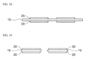
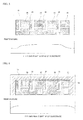
FIGS. 1A to 1F are schematic views illustrating the process of manufacturing a metal-bonding ceramic substrate. -
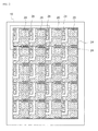
FIG. 2 is a plan view of a conventional metal-bonding ceramic substrate. -
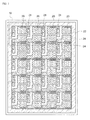
FIG. 3 is a plan view of a metal-bonding ceramic substrate according to an exemplary embodiment of the present invention. -
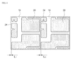
FIG. 4 is an enlarged view of parts drawn by dotted lines inFIGS. 2 and3 . -
FIG. 5 is a graph schematically showing the temperature distribution in thermal treatment of the conventional metal-bonding ceramic substrate. -
FIG. 6 is a graph schematically showing the temperature distribution in thermal treatment of the metal-bonding ceramic substrate according to the exemplary embodiment of the present invention. -
FIG. 7 is an X-ray image after thermal treatment of a lead ash layer on a metal-bonding ceramic substrate. -
FIG. 8 is a graph schematically showing the stress distribution on the upper and lower surfaces of the conventional metal-bonding ceramic substrate. -
FIG. 9 is a schematic view of a conventional metal-bonding ceramic substrate that is bent. -
FIG. 10 is a plan view of a metal-bonding ceramic substrate according to another exemplary embodiment of the present invention. -
FIG. 11 is a plan view of a metal-bonding ceramic substrate according to still another exemplary embodiment of the present invention. - Hereinafter, an exemplary embodiment of a metal-bonding ceramic substrate according to the present invention will be described in detail with respect to the accompanying drawings.
- Before describing, the configuration denoted by
reference numeral 10 is expressed as both terms, for example, a ceramic substrate and a metal-bonding ceramic substrate, and the configuration denoted byreference numeral 20 is expressed as both terms, for example, a metal or a metal layer. - First, the process of manufacturing a metal-bonding ceramic substrate will be described with reference to
FIGS. 1A to 1F . According to the general process of manufacturing a metal-bonding ceramic substrate, ametal 20 is contact-disposed on aceramic substrate 10, they are bonded together by a DBC or active metal method as shown inFIG. 1A , and the metal-bondingceramic substrate 10, manufactured by such bonding, is coated with aphotosensitive film 30, which is a dry film, to cure a desired part by UV exposure (SeeFIG. 1B ). - Subsequently, an uncured part of the
metal layer 20 formed by bonding to theceramic substrate 10 is developed as shown inFIG. 1C , and a circuit pattern is formed on theceramic substrate 10 through an etching process for removing an unnecessary part by an acid chemical (SeeFIG. 1D ). In addition, thephotosensitive film 30 is removed by a peeling process (SeeFIG. 1E ), and finally, the circuit pattern is formed using themetal layer 20 bonded to theceramic substrate 10 through an etching process. - Lastly, the circuit pattern is uniformly disposed on the
ceramic substrate 10 and is cut into pieces by melting the ceramic using a carbon dioxide laser generating strong photoenergy (SeeFIG. 1F ). The metal-bondingceramic substrate 10 manufactured according to the manufacturing method described above may be designed in various arrangements according to the designing methods by manufacturers or requests by consumers. - For example, circuit patterns may be symmetrically formed by bonding the
metal layers 20 to both surfaces of theceramic substrate 10, or a circuit pattern is formed on one surface of theceramic substrate 10 and themetal layer 20, not a circuit pattern, may be formed entirely on the other surface of theceramic substrate 10. - Next,
FIG. 2 is a plan view of a conventional metal-bonding ceramic substrate, andFIG. 3 is a plan view of a metal-bonding ceramic substrate according to an exemplary embodiment of the present invention. - Referring to
FIGS. 2 and3 , the conventional metal-bonding ceramic substrate is compared with the metal-bonding ceramic substrate according to the present invention. In a prior art, the plurality ofmetal layers 20 may be disposed in rows and columns on one surface of aceramic substrate 10. Here, all themetal layers 20 having no circuit pattern formed therein are removed. That is, unnecessary parts which are on the edge of themetal layer 20 are all removed. However, referring toFIG. 3 , anadditional metal layer 22 is bonded to the outside of themetal layer 20 in the metal-bonding ceramic substrate according to the present invention. - The
ceramic substrate 10 and themetal layer 20 may be formed of various materials. For example, theceramic substrate 10 may be formed of a ceramic material such as alumina (Al2O3), aluminum nitride (AlN), silicon carbide (SiC) or silicon nitride (Si3N4), and themetal layer 20 is formed of copper (Cu) or aluminum (Al). - The
additional metal layer 22 may be formed along an edge of theceramic substrate 10 by bonding to at least one surface of theceramic substrate 10. Theadditional metal layer 22 surrounds the edge of themetal layer 20 in a strap shape. Theadditional metal layer 22 formed as described above can improve dimension precision of theceramic substrate 10 and can improve the bonding property of a semiconductor chip by reducing the temperature variation in thermal treatment. Detailed descriptions about these characteristics will be provided below. - Meanwhile, the cutting
line 24 is formed between the metal layers 20. In addition, the cuttingline 24 is also formed between themetal layer 20 and theadditional metal layer 22. The cuttingline 24 is a part formed to facilitate cutting themetal layer 20. - In the exemplary embodiment of the present invention, to improve the dimension precision of the
ceramic substrate 10, the distance between the metal layers 20 may be the same as the distance between theoutermost metal layer 20 and theadditional metal layer 22. In addition, the cuttingline 24 is formed at a central region between the metal layers 20, and the central region between theoutermost metal layer 20 and theadditional metal layer 22. -
FIG. 4 is an enlarged view of parts drawn by dotted lines inFIGS. 2 and3 . - Referring to
FIG. 4 , it is assumed that the distance between theoutermost metal layer 20 and the cuttingline 24 refers to dimension 1 (L1), and the distance between theinner metal layer 20 and the cuttingline 24 refers to dimension 2 (L2). - Since the precision of a circuit pattern is a very important factor in the metal-
bonding ceramic substrate 10, in the past, the shape of the circuit pattern was pressed using a mold and was directly bonded to a single substrate. However, in recent years, as described inFIG. 1 , the desired circuit pattern is left intact using an etching process, but unnecessary parts are removed by a chemical reaction. Here, since the conventional metal-bonding ceramic substrate 10 does not have anadditional metal layer 22 formed on the edge thereof (inFIG. 2 ), etching progressed on the edge more rapidly than in the central region (a part having the metal layer), and thusdimension 1 was always larger thandimension 2. - However, since the metal-
bonding ceramic substrate 10 according to the present invention has theadditional metal layer 22 formed on the edge thereof (inFIG. 3 ), etching may progress under the same condition as in the central region (the part having the metal layer). Accordingly,dimension 1 anddimension 2 may be the same as each other in the metal-bonding ceramic substrate 10 according to the present invention, and thus the dimension precision of the circuit pattern may be enhanced. - Table 1 shows circuit dimensions of metal-bonding ceramic substrates. While in the conventional metal-bonding ceramic substrate,
dimension 1 is approximately 0.1 mm larger thandimension 2 and in thepresent invention dimension 1 is almost the same asdimension 2. This is because the conventional metal-bonding ceramic substrate is different from the metal-bonding ceramic substrate according to the present invention in that the same environments are not provided to the adjacent regions in etching themetal layer 20 in the case of the conventional metal-bonding ceramic substrate, but the metal layers 20 are disposed at the same distance from the adjacent regions in the case of the metal-bonding ceramic substrate according to the present invention.[Table 1] No. Conventional Inventive Dimension 1 Dimension 2Dimension 1Dimension 2Set Value 0.6 0.6 0.6 0.6 I 0.702 0.613 0.608 0.611 2 0.712 0.610 0.604 0.608 3 0.708 0.621 0.602 0.620 4 0.692 0.619 0.609 0.622 5 0.699 0.601 0.611 0.601 6 0.705 0.602 0.622 0.598 7 0.712 0.605 0.611 0.621 8 0.705 0.607 0.617 0.609 9 0.704 0.611 0.611 0.611 10 0.698 0.605 0.608 0.624 Average 0.704 0.609 0.610 0.613 - Subsequently,
FIG. 5 is a graph schematically showing the temperature distribution in thermal treatment of the conventional metal-bonding ceramic substrate, andFIG. 6 is a graph schematically showing the temperature distribution in thermal treatment of the metal-bonding ceramic substrate according to the exemplary embodiment of the present invention. - Referring to
FIGS. 5 and 6 , to mount a semiconductor chip on the metal-bonding ceramic substrate, a lead ash layer is formed on the surface of the ceramic substrate using a printing method, a semiconductor chip is disposed on the lead ash layer, and they are then bonded to each other. Here, the semiconductor chip may be strongly bonded to theceramic substrate 10 when the lead ash layer melts in continuous thermal treatment equipment in which the temperature is maintained at 150 to 350 °C for approximately 10 to 30 min. - Here, depending on the variation of the temperature applied to the
ceramic substrate 10 in the thermal treatment, there is a difference in the melting degree of the lead ash layer. When there is a wide temperature variation, the lead ash layer does not melt, so that the bonding between the ceramic substrate and the semiconductor chip may not be properly executed, and when excessive heat is concentrated on theceramic substrate 10, a void may be generated in theceramic substrate 10 due to the spreading of the lead ash layer so that a bonding property decreases. - Referring to
FIG. 5 , since theadditional metal layer 22 is not formed on the edge of the conventional metal-bonding ceramic substrate, there may be a difference in temperature distribution in a single substrate so that the bonding property of the lead ash layer decreases in the thermal treatment as described above. - However, referring to
FIG. 6 , since theadditional metal layer 22 is formed on the edge of the metal-bonding ceramic substrate according to the present invention, the temperature is relatively uniformly distributed in a width direction of theceramic substrate 10. Therefore, the lead ash layer melts uniformly in the thermal treatment, and thus the bonding property of the lead ash layer may be enhanced, and thermal treatment characteristics may be improved. - Referring to
FIG. 7 , the actual area of the bonded lead ash layer when there is a difference in temperature distribution according to the conventional art is imaged using X-rays. It can be confirmed that there are unbonded parts and internal voids. - Table 2 shows wettability of the lead ash layer in location (1) and location (2) shown in
FIG. 7 . Referring to Table 2, in the conventional art, the difference between location (1) (edge) and location (2) (central region) is approximately 10%, which considerably reduces the bonding property with the semiconductor chip and adversely affects selection of the process condition. However, in the present invention, the difference between location (1) and location (2) is approximately less than 1%, and average wettabiltiy is less than 5%, so that the wettaiblity is considerably improved compared to the conventional art.[Table 2] No. Conventional Inventive Location 1 Location 2Location 1Location 21 21.4% 11.2% 4.2% 3.8% 2 18.5% 8.0% 3.6% 3.4% 3 19.5% 8.8% 5.4% 3.9% 4 21.2% 5.5% 4.8% 3.8% 5 18.8% 9.8% 4.2% 3.2% 6 17.5% 8.5% 4.8% 3.6% 7 19.2% 7.6% 5.5% 3.7% 8 20.1% 9.8% 4.5% 3.5% 9 20.5% 10.2% 3.8% 3.7% 10 22.6% 8.4% 4.1% 3.8% Average 19.93% 8.78% 4.49% 3.64% - Next,
FIG. 8 is a graph schematically showing the stress distribution on the upper and lower surfaces of the conventional metal-bonding ceramic substrate, andFIG. 9 is a schematic view of the conventional metal-bonding ceramic substrate which is bent. - Generally, a semiconductor diode is mounted on the upper surface of the metal-bonding ceramic substrate, and various types of circuit patterns for connecting a circuit to a circuit and a circuit to a semiconductor diode through wire bonding are realized. On the other hand, a simple rectangular pattern, not a complicated pattern, is formed on the lower surface of the metal-bonding ceramic substrate to effectively radiate heat to a part bonded with the radiator.
- Referring to
FIG. 8 , the stress distribution is differently shown on the upper and lower surfaces of the conventional metal-bonding ceramic substrate due to a large difference in the coefficient of the thermal expansion between copper (approximately 16.7 x 10⁻⁶/°C) and ceramic (AIN: 4.6x10⁻⁶/°C, Alumina: 6.8x10⁻⁶/°C). That is, it can be seen that stress is relieved on the upper surface having various circuit patterns, and large stress is generated on the entire lower surface since there is no disconnection of the circuit pattern. - The conventional metal-bonding ceramic substrate is bent by the stress distribution as shown in
FIG. 9 . In the present invention, to minimize bending, theadditional metal layer 22 is further formed as described above. As theadditional metal layer 22 that is formed as described above has various areas and shapes, the ceramic substrate may be bent less, and the bending of the ceramic substrate may be controlled in a desired direction. - Meanwhile,
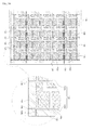
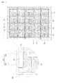
FIG. 10 is a plan view of a metal-bonding ceramic substrate according to another exemplary embodiment of the present invention, andFIG. 11 is a plan view of a metal-bonding ceramic substrate according to still another exemplary embodiment of the present invention. In the drawings, the same components as in the exemplary embodiment described above are denoted by reference numerals of hundreds, and detailed descriptions thereof will be omitted. - First, referring to
FIG. 10 , unlike the exemplary embodiment described above,additional metal layers 122 are not connected by means of one strap, and the cuttingchannel 124 is formed between the additional metal layers 122. The cuttingchannel 124 is a part corresponding to the extension of a boundary between metal layers 120. - The
cutting line 130 is composed of aninternal cutting line 130a and anexternal cutting line 130b. Theexternal cutting line 130b is a cutting line disposed at the edge (the outermost layer) of a plurality of the metal layers 120 disposed in rows and columns, and theinternal cutting line 130a is a cutting line formed between the metal layers 122 as a cutting line disposed inside. - In the exemplary embodiment illustrated in
FIG. 10 , theinternal cutting line 130a does not extend to the cuttingchannel 124, but theexternal cutting line 130 extends to the cuttingchannel 124. Here, the entireexternal cutting line 130b may not extend to the cuttingchannels 124, but only parts corresponding to both ends (upper and lower ends or left and right ends inFIG. 10 ) of theexternal cutting line 130b extend to the cuttingchannels 124. That is, at least parts of theexternal cutting line 130b extend to the cuttingchannels 124. It is to cut first the parts corresponding to both ends of theexternal cutting line 130b when theadditional metal layer 22 is cut, and to prevent random cutting of theadditional metal layer 122 perpendicularly disposed from themetal layer 120 after theexternal cutting line 130b is cut. - Subsequently, in the exemplary embodiment illustrated in
FIG. 11 , all of the external andinternal cutting lines ceramic substrate 110 through a cuttingchannel 124. - While the invention has been shown and described with reference to certain exemplary embodiments thereof, it will be understood by those skilled in the art that various changes in form and details may be made therein without departing from the scope of the invention as defined by the appended claims.
Claims (9)
- A metal-bonding ceramic substrate, comprising a metal layer bonded on the surface thereof to form a circuit pattern, the metal layer being plural in number and disposed in rows and columns,
wherein an additional metal layer is formed along an edge of at least one surface of the ceramic substrate to be disposed on the outside of the metal layer. - The metal-bonding ceramic substrate according to Claim 1, wherein the distance between metal layers is the same as that between the outermost metal layer and the additional metal layer.
- The metal-bonding ceramic substrate according to Claim 1, wherein at least one cutting line is formed between the metal layers and between the metal layer and the additional metal layer.
- The metal-bonding ceramic substrate according to Claim 3, wherein the cutting line is comprising an external cutting line formed at the edge of the metal layer and an internal cutting line formed between the metal layers.
- The metal-bonding ceramic substrate according to Claim 4, wherein the additional metal layer has a cutting channel formed at a part corresponding to the extension of the boundary of the metal layers, which are plural in number and disposed in rows and columns.
- The metal-bonding ceramic substrate according to Claim 5, wherein the internal cutting line extends only to the edge of the metal layer, and the external cutting line extends to the edge of the ceramic substrate through the cutting channel.
- The metal-bonding ceramic substrate according to Claim 5, wherein the external and internal cutting lines extend to the edge of the ceramic substrate through the cutting channel.
- The metal-bonding ceramic substrate according to Claim 1, wherein the ceramic substrate is formed of a ceramic material such as alumina (Al2O3), aluminum nitride (AlN), silicon carbide (SiC) or silicon nitride (Si3N4), and the metal layer is formed of copper or aluminum.
- The metal-bonding ceramic substrate according to Claim 1, wherein the additional metal layer is formed on upper and lower surfaces of the ceramic substrate to have different areas and shapes.
Applications Claiming Priority (2)
| Application Number | Priority Date | Filing Date | Title |
|---|---|---|---|
| KR1020100020879A KR101675727B1 (en) | 2010-03-09 | 2010-03-09 | Metal bonded ceramic substrate |
| PCT/KR2011/001609 WO2011111989A2 (en) | 2010-03-09 | 2011-03-09 | Metal-bonded ceramic substrate |
Publications (2)
| Publication Number | Publication Date |
|---|---|
| EP2546870A2 true EP2546870A2 (en) | 2013-01-16 |
| EP2546870A4 EP2546870A4 (en) | 2017-11-29 |
Family
ID=44563992
Family Applications (1)
| Application Number | Title | Priority Date | Filing Date |
|---|---|---|---|
| EP11753594.8A Withdrawn EP2546870A4 (en) | 2010-03-09 | 2011-03-09 | Metal-bonded ceramic substrate |
Country Status (4)
| Country | Link |
|---|---|
| EP (1) | EP2546870A4 (en) |
| JP (1) | JP5642808B2 (en) |
| KR (1) | KR101675727B1 (en) |
| WO (1) | WO2011111989A2 (en) |
Cited By (1)
| Publication number | Priority date | Publication date | Assignee | Title |
|---|---|---|---|---|
| CN117116775A (en) * | 2023-09-25 | 2023-11-24 | 江苏富乐华半导体科技股份有限公司 | A graphic design method for thick metal layer ceramic substrates |
Families Citing this family (8)
| Publication number | Priority date | Publication date | Assignee | Title |
|---|---|---|---|---|
| JP2719412B2 (en) | 1989-08-02 | 1998-02-25 | 三洋電機株式会社 | Infrared control device |
| KR101733442B1 (en) * | 2014-12-29 | 2017-05-10 | 주식회사 케이씨씨 | Warpage-preventing structure of substrate |
| CN108059485B (en) * | 2017-12-05 | 2023-06-13 | 上海铠琪科技有限公司 | Miniature ultrathin aluminum nitride ceramic circuit board and preparation method thereof |
| US20210212214A1 (en) * | 2018-05-23 | 2021-07-08 | Sumitomo Bakelite Co., Ltd. | Method of manufacturing circuit board |
| JP7122461B2 (en) * | 2019-03-25 | 2022-08-19 | 京セラ株式会社 | Circuit board and heat dissipation board or electronic device provided with the same |
| KR20200127511A (en) * | 2019-05-02 | 2020-11-11 | 주식회사 아모센스 | Ceramic substrate and manufacturing method for the same |
| KR102244833B1 (en) | 2019-12-10 | 2021-04-27 | 주식회사 유텔 | Stacked lcp electronic device |
| CN113764292B (en) * | 2021-11-08 | 2022-03-01 | 上海曦智科技有限公司 | Semiconductor device and method for manufacturing the same |
Family Cites Families (8)
| Publication number | Priority date | Publication date | Assignee | Title |
|---|---|---|---|---|
| EP0398485B1 (en) * | 1989-05-16 | 1995-08-09 | Gec-Marconi Limited | A method of making a Flip Chip Solder bond structure for devices with gold based metallisation |
| JP2876989B2 (en) * | 1994-05-31 | 1999-03-31 | 松下電工株式会社 | Manufacturing method of printed wiring board |
| JP4077888B2 (en) * | 1995-07-21 | 2008-04-23 | 株式会社東芝 | Ceramic circuit board |
| US6261703B1 (en) * | 1997-05-26 | 2001-07-17 | Sumitomo Electric Industries, Ltd. | Copper circuit junction substrate and method of producing the same |
| JP4168114B2 (en) * | 2001-09-28 | 2008-10-22 | Dowaホールディングス株式会社 | Metal-ceramic joint |
| JP2007019123A (en) * | 2005-07-06 | 2007-01-25 | Sumitomo Metal Electronics Devices Inc | Ceramic circuit board assembly |
| JP3993619B2 (en) * | 2005-07-06 | 2007-10-17 | 株式会社住友金属エレクトロデバイス | Ceramic circuit board assembly |
| JP2007324277A (en) * | 2006-05-31 | 2007-12-13 | Sumitomo Metal Electronics Devices Inc | Ceramic circuit board assembly |
-
2010
- 2010-03-09 KR KR1020100020879A patent/KR101675727B1/en active Active
-
2011
- 2011-03-09 EP EP11753594.8A patent/EP2546870A4/en not_active Withdrawn
- 2011-03-09 JP JP2012556974A patent/JP5642808B2/en active Active
- 2011-03-09 WO PCT/KR2011/001609 patent/WO2011111989A2/en not_active Ceased
Non-Patent Citations (1)
| Title |
|---|
| See references of WO2011111989A2 * |
Cited By (2)
| Publication number | Priority date | Publication date | Assignee | Title |
|---|---|---|---|---|
| CN117116775A (en) * | 2023-09-25 | 2023-11-24 | 江苏富乐华半导体科技股份有限公司 | A graphic design method for thick metal layer ceramic substrates |
| CN117116775B (en) * | 2023-09-25 | 2024-03-26 | 江苏富乐华半导体科技股份有限公司 | Graphic design method of thick metal layer ceramic substrate |
Also Published As
| Publication number | Publication date |
|---|---|
| KR20110101692A (en) | 2011-09-16 |
| KR101675727B1 (en) | 2016-11-14 |
| JP2013522872A (en) | 2013-06-13 |
| EP2546870A4 (en) | 2017-11-29 |
| WO2011111989A3 (en) | 2012-01-05 |
| JP5642808B2 (en) | 2014-12-17 |
| WO2011111989A2 (en) | 2011-09-15 |
Similar Documents
| Publication | Publication Date | Title |
|---|---|---|
| KR101675727B1 (en) | Metal bonded ceramic substrate | |
| EP3608951B1 (en) | Ceramic metal circuit board and semiconductor device using the same | |
| US9887173B2 (en) | Method for producing structured sintered connection layers, and semiconductor element having a structured sintered connection layer | |
| JP6706253B2 (en) | POWER MODULE SUBSTRATE, POWER MODULE SUBSTRATE ASSEMBLY, AND POWER MODULE SUBSTRATE MANUFACTURING METHOD | |
| EP3358615B1 (en) | Silicon nitride circuit board and semiconductor module using same | |
| US9905529B2 (en) | Method for manufacturing semiconductor device | |
| WO2013021750A1 (en) | Wiring substrate and method for manufacturing same and semiconductor device | |
| JP3347279B2 (en) | Semiconductor device and method of manufacturing the same | |
| KR20170048999A (en) | Ceramic Board Manufacturing Method and Ceramic Board manufactured by thereof | |
| WO2020038554A1 (en) | Forming a semiconductor device with heat conduction layers formed by laser direct structuring | |
| CN1392602A (en) | Method for producing circuit device | |
| KR101733442B1 (en) | Warpage-preventing structure of substrate | |
| JP2004307307A (en) | Ceramic circuit board and method of manufacturing the same | |
| KR101280250B1 (en) | Metal-bonded ceramic substrate | |
| US20230254970A1 (en) | Circuit board | |
| US12114417B2 (en) | Circuit board | |
| US12402246B2 (en) | Circuit board | |
| KR101900547B1 (en) | Loading system for producing ceramic substrate and method of producing ceramic board using thereof | |
| JP2000058723A (en) | Circuit board | |
| JP2004140199A (en) | Module structure and manufacturing method thereof | |
| JP6809945B2 (en) | Manufacturing method of metal-ceramic circuit board | |
| TW202406426A (en) | Printed-circuit-board structure and method for manufacturing | |
| JP2000086367A (en) | Joint and circuit board using the same | |
| JP2021052056A (en) | Circuit board and power module | |
| TW200522304A (en) | Electronic assembly having a die with rounded corner edge portions and a method of fabricating the same |
Legal Events
| Date | Code | Title | Description |
|---|---|---|---|
| PUAI | Public reference made under article 153(3) epc to a published international application that has entered the european phase |
Free format text: ORIGINAL CODE: 0009012 |
|
| 17P | Request for examination filed |
Effective date: 20121004 |
|
| AK | Designated contracting states |
Kind code of ref document: A2 Designated state(s): AL AT BE BG CH CY CZ DE DK EE ES FI FR GB GR HR HU IE IS IT LI LT LU LV MC MK MT NL NO PL PT RO RS SE SI SK SM TR |
|
| DAX | Request for extension of the european patent (deleted) | ||
| A4 | Supplementary search report drawn up and despatched |
Effective date: 20171027 |
|
| RIC1 | Information provided on ipc code assigned before grant |
Ipc: C04B 37/02 20060101AFI20171023BHEP |
|
| STAA | Information on the status of an ep patent application or granted ep patent |
Free format text: STATUS: EXAMINATION IS IN PROGRESS |
|
| 17Q | First examination report despatched |
Effective date: 20191125 |
|
| STAA | Information on the status of an ep patent application or granted ep patent |
Free format text: STATUS: THE APPLICATION IS DEEMED TO BE WITHDRAWN |
|
| 18D | Application deemed to be withdrawn |
Effective date: 20210224 |