EP2546623A2 - Infrared sensor chip, infrared detector and an operating method and test method therefor - Google Patents
Infrared sensor chip, infrared detector and an operating method and test method therefor Download PDFInfo
- Publication number
- EP2546623A2 EP2546623A2 EP12748373A EP12748373A EP2546623A2 EP 2546623 A2 EP2546623 A2 EP 2546623A2 EP 12748373 A EP12748373 A EP 12748373A EP 12748373 A EP12748373 A EP 12748373A EP 2546623 A2 EP2546623 A2 EP 2546623A2
- Authority
- EP
- European Patent Office
- Prior art keywords
- switch
- output multiplexer
- cell
- reference cell
- infrared sensor
- Prior art date
- Legal status (The legal status is an assumption and is not a legal conclusion. Google has not performed a legal analysis and makes no representation as to the accuracy of the status listed.)
- Withdrawn
Links
Images




Classifications
-
- G—PHYSICS
- G01—MEASURING; TESTING
- G01J—MEASUREMENT OF INTENSITY, VELOCITY, SPECTRAL CONTENT, POLARISATION, PHASE OR PULSE CHARACTERISTICS OF INFRARED, VISIBLE OR ULTRAVIOLET LIGHT; COLORIMETRY; RADIATION PYROMETRY
- G01J5/00—Radiation pyrometry, e.g. infrared or optical thermometry
- G01J5/02—Constructional details
-
- G—PHYSICS
- G01—MEASURING; TESTING
- G01J—MEASUREMENT OF INTENSITY, VELOCITY, SPECTRAL CONTENT, POLARISATION, PHASE OR PULSE CHARACTERISTICS OF INFRARED, VISIBLE OR ULTRAVIOLET LIGHT; COLORIMETRY; RADIATION PYROMETRY
- G01J5/00—Radiation pyrometry, e.g. infrared or optical thermometry
- G01J5/02—Constructional details
- G01J5/026—Control of working procedures of a pyrometer, other than calibration; Bandwidth calculation; Gain control
-
- G—PHYSICS
- G01—MEASURING; TESTING
- G01J—MEASUREMENT OF INTENSITY, VELOCITY, SPECTRAL CONTENT, POLARISATION, PHASE OR PULSE CHARACTERISTICS OF INFRARED, VISIBLE OR ULTRAVIOLET LIGHT; COLORIMETRY; RADIATION PYROMETRY
- G01J5/00—Radiation pyrometry, e.g. infrared or optical thermometry
- G01J5/10—Radiation pyrometry, e.g. infrared or optical thermometry using electric radiation detectors
- G01J5/20—Radiation pyrometry, e.g. infrared or optical thermometry using electric radiation detectors using resistors, thermistors or semiconductors sensitive to radiation, e.g. photoconductive devices
-
- G—PHYSICS
- G01—MEASURING; TESTING
- G01J—MEASUREMENT OF INTENSITY, VELOCITY, SPECTRAL CONTENT, POLARISATION, PHASE OR PULSE CHARACTERISTICS OF INFRARED, VISIBLE OR ULTRAVIOLET LIGHT; COLORIMETRY; RADIATION PYROMETRY
- G01J5/00—Radiation pyrometry, e.g. infrared or optical thermometry
- G01J5/10—Radiation pyrometry, e.g. infrared or optical thermometry using electric radiation detectors
- G01J5/20—Radiation pyrometry, e.g. infrared or optical thermometry using electric radiation detectors using resistors, thermistors or semiconductors sensitive to radiation, e.g. photoconductive devices
- G01J5/22—Electrical features thereof
- G01J5/24—Use of specially adapted circuits, e.g. bridge circuits
-
- H—ELECTRICITY
- H10—SEMICONDUCTOR DEVICES; ELECTRIC SOLID-STATE DEVICES NOT OTHERWISE PROVIDED FOR
- H10W—GENERIC PACKAGES, INTERCONNECTIONS, CONNECTORS OR OTHER CONSTRUCTIONAL DETAILS OF DEVICES COVERED BY CLASS H10
- H10W72/00—Interconnections or connectors in packages
- H10W72/50—Bond wires
- H10W72/541—Dispositions of bond wires
- H10W72/5445—Dispositions of bond wires being orthogonal to a side surface of the chip, e.g. parallel arrangements
-
- H—ELECTRICITY
- H10—SEMICONDUCTOR DEVICES; ELECTRIC SOLID-STATE DEVICES NOT OTHERWISE PROVIDED FOR
- H10W—GENERIC PACKAGES, INTERCONNECTIONS, CONNECTORS OR OTHER CONSTRUCTIONAL DETAILS OF DEVICES COVERED BY CLASS H10
- H10W90/00—Package configurations
- H10W90/701—Package configurations characterised by the relative positions of pads or connectors relative to package parts
- H10W90/751—Package configurations characterised by the relative positions of pads or connectors relative to package parts of bond wires
- H10W90/753—Package configurations characterised by the relative positions of pads or connectors relative to package parts of bond wires between laterally-adjacent chips
Definitions
- Another embodiment is a parametric testing method of an infrared sensor including an active cell and a reference cell.
- the method includes: receiving sequentially values of current flowing through the reference cell and the active cell by controlling in manner that a first switch and a second switch are alternately on/off states, wherein the first switch which selectively connects the reference cell with one input terminal of an output multiplexer and wherein the second switch which selectively connects the active cell with the one input terminal of the output multiplexer; and measuring resistance values of the reference cell and the active cell on the basis of the current values and a voltage applied to both ends of the reference cell and the active cell.
- the switching unit 310 may be implemented by a switching element such as NMOS transistor, PMOS transistor, CMOS transistor and the like.
- the address control logic unit 300 may be implemented by a shift register for sequentially applying addresses to the switching unit 310 and by a multiplexer and the like for randomly applying addresses.
- the column line selection switches 640a to 640n are connected to routing lines 650a to 650n. Therefore, the electrical signals generated by the bolometers 620a to 620n are externally outputted through the analog current signal output unit 330.
- the flip-flop 1000 is connected to a row signal line 1010, a row clock line 1020 and a reset line 1030. As shown in Fig. 5 , control signals such as row signal, row clock, reset and the like are inputted through the lines 1010, 1020 and 1030 connected to the analog current signal output unit 330.
- Fig. 12 is a circuit diagram showing current flows when the circuit diagram of Fig. 10 is in an operation mode, the first switch P1 and the third switch N2 operate in a saturation area of the transistor, and the second switch N1 operates in a linear area of the transistor.
- a device (not shown) for amplifying the current difference may be further included in the front end of the input terminal of the output multiplexer 600a.
- resistance values of the reference cell 610 and the active cell 620 are measured respectively and a statistical monitoring is performed. It is judged whether the sensor is defective or not, and then a good die is selected.
Landscapes
- Physics & Mathematics (AREA)
- General Physics & Mathematics (AREA)
- Spectroscopy & Molecular Physics (AREA)
- Photometry And Measurement Of Optical Pulse Characteristics (AREA)
- Semiconductor Integrated Circuits (AREA)
- Solid State Image Pick-Up Elements (AREA)
Abstract
Description
- The present invention relates to an infrared sensor chip, an infrared detector and a method for operating and testing the same.
- A bolometer-type infrared detector has resistance characteristics, varying depending on a temperature. The infrared sensor includes a sensor (for example, a bolometer) and a read out integrated circuit (ROIC) for processing signals according to the amount of infrared rays detected by the sensor.
- A conventional infrared detector is manufactured on a wafer substrate by designing in advance the ROIC on the wafer substrate and by using a MEMS process.
- Therefore, since the ROIC is designed in advance on the wafer and the sensor is manufactured on the ROIC, it is not easy to previously check the operation state of the sensor.
- Also, since the sensor and the ROIC are connected to each other by using a monolithic method, the degree of integration of a chip is low and the wafer and/or the infrared detector cannot be reused when defective, so that there is a disadvantage in that cost is increased.
- The present invention is provided to overcome the above-mentioned problems of the prior art. The present invention removes interference between the bolometer and the ROIC chip and makes it possible to test the wafer or the chip level.
- The objective of the present invention is to improve the manufacturing yield through process monitoring and minimize the cost caused by defections by reducing the manufacturing cost of the infrared detector and by checking in advance the operation state of the sensor and/or the ROIC.
- One embodiment is an infrared sensor chip. The infrared sensor chip includes: a CMOS circuit board comprised of an active matrix, a row line selector and an output multiplexer; and a bolometer which is stacked on the CMOS circuit board and is comprised of an active cell and a reference cell, wherein, for the purpose of a parametric test for the bolometer at a wafer or chip level, the row line selector selects a cell to which a voltage is applied in the bolometer, and wherein the output multiplexer outputs current characteristics according to the voltage application.
- A first switch and a second switch may be on/off controlled respectively by a control signal. The first switch selectively connects the reference cell with one input terminal of the output multiplexer. The second switch selectively connects the active cell with the one input terminal of the output multiplexer.
- When the first switch and the second switch are on/off controlled respectively, a value of current flowing through one of the reference cell and the active cell may be outputted through the output multiplexer.
- The first switch which selectively connects the reference cell with one input terminal of the output multiplexer and the second switch which selectively connects the active cell with the one input terminal of the output multiplexer may be controlled by an independent analog control signal and may operate in a saturation area. A difference between currents flowing through the reference cell and the active cell may be inputted as it is or may be amplified by an amplifier and inputted to one input terminal of the output multiplexer.
- Another embodiment is a parametric testing method of an infrared sensor including an active cell and a reference cell. The method includes: receiving sequentially values of current flowing through the reference cell and the active cell by controlling in manner that a first switch and a second switch are alternately on/off states, wherein the first switch which selectively connects the reference cell with one input terminal of an output multiplexer and wherein the second switch which selectively connects the active cell with the one input terminal of the output multiplexer; and measuring resistance values of the reference cell and the active cell on the basis of the current values and a voltage applied to both ends of the reference cell and the active cell.
- An independent variable analog power control signal for the on/off control may be inputted to the first switch and the second switch respectively.
- Further another embodiment is an operating method of an infrared sensor including an active cell and a reference cell. The method includes: applying an independent variable analog power control signal to a first switch which selectively connects the reference cell with one input terminal of an output multiplexer; applying an independent variable analog power control signal to a second switch which selectively connects the active cell with the one input terminal of the output multiplexer; and outputting externally a difference between currents flowing through the reference cell and the active cell through the output multiplexer such that the difference is outputted as it is or is amplified and outputted.
- Yet another embodiment is an infrared detector including: an infrared sensor chip which includes a circuit board including a row line selector and an output multiplexer, an infrared sensor which is stacked on the circuit board and includes a plurality of cells which are selected by a signal from the row line selector and output a current signal related to infrared detection to the output multiplexer; and a Sa-FPA controller chip which is electrically connected to the infrared sensor chip and applies a signal controlling the row line selector and the output multiplexer, and reads the current signal transmitted from the output multiplexer.
- The Sa-FPA controller chip may be integrated with an image signal processing (ISP) chip.
- The Sa-FPA controller chip may be integrated with a DAC variable analog power chip.
- According to the present invention, an infrared sensor chip without a Sa-FPA controller chip is separately manufactured, so that a bolometer of a wafer or a chip level can be tested, and thus it is possible to minimize the cost caused by defections.
- Also, according to the present invention, it is possible to reduce the manufacturing cost of the infrared detector and to shorten time required for developing the infrared detector. The manufacturing yield can be also improved through process monitoring.
-
-
Fig. 1 is a conceptual diagram for schematically describing a configuration of an infrared detector using Sa-FPA according to an embodiment of the present invention; -
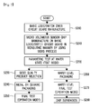
Fig. 2 is a flowchart showing a manufacturing process of the infrared detector using Sa-FPA according to the embodiment of the present invention; -
Figs. 3 and 4 are block diagrams showing the manufacturing process one by one of the infrared detector using Sa-FPA according to the flowchart ofFig. 2 ; -
Fig. 5 is a circuit diagram showing the configuration of the infrared detector according to the embodiment of the present invention; -
Fig. 6 is a circuit diagram of a row control shift register in the circuit diagram shown inFig. 5 ; -
Fig. 7 is a circuit diagram of a column control shift register in the circuit diagram shown inFig. 5 ; -
Fig. 8 is another circuit diagram of an infrared sensor chip according to the embodiment of the present invention; -
Fig. 9 is a block diagram for describing the operation mode and test mode of the infrared sensor chip according to the embodiment of the present invention; -
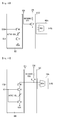
Figs. 10 and 11 are circuit diagrams showing configurations of the infrared sensor and an output multiplexer in the block diagram ofFig. 9 ; and -
Fig. 12 is a circuit diagram showing signal flows when the circuit diagram ofFig. 10 is in an operation mode. - As the present invention can have various embodiments as well as can be diversely changed, specific embodiments will be illustrated in the drawings and described in detail. While the present invention is not limited to particular embodiments, all modification, equivalents and substitutes included in the spirit and scope of the present invention are understood to be included therein. In the drawings, similar reference numerals are used to designate similar components. While terms such as the first and the second, etc., can be used to describe various components, the components are not limited by the terms mentioned above. The terms are used only for distinguishing between one component and other components. For example, the first component may be designated as the second component without departing from the scope of rights of the invention. Similarly, the second component may be designated as the first component. The term of 'and/or' includes a combination or one of a plurality of related items mentioned.
- In the case where a component is referred to as being "connected" or "accessed" to other component, it should be understood that not only the component is directly connected or accessed to the other component, but also there may exist another component between them. Meanwhile, in the case where a component is referred to as being "directly connected" or "directly accessed" to other component, it should be understood that there is no component therebetween.
- Terms used in the present specification are provided for description of only specific embodiments of the present invention, and not intended to be limiting. An expression of a singular form includes the expression of plural form thereof unless otherwise explicitly mentioned in the context. In the present specification, it should be understood that the term "include" or "comprise" and the like is intended to specify characteristics, numbers, steps, operations, components, parts or any combination thereof which are mentioned in the specification, and intended not to previously exclude the possibility of existence or addition of at least one another characteristics, numbers, steps, operations, components, parts or any combination thereof.
- Unless differently defined, all terms used herein including technical and scientific terms have the same meaning as commonly understood by one of ordinary skill in the art to which the present invention belongs. Terms, for example, commonly used terms defined in the dictionary, are to be construed to have exactly the same meaning as that of related technology in the context. As long as terms are not clearly defined in the present application, the terms should not be ideally or excessively construed as formal meaning.
- Hereafter, an infrared detector which is manufactured by using Sa-FPA according to an embodiment of the present invention and a method for manufacturing the same will be described in detail.
-
Fig. 1 is a conceptual diagram for schematically describing the entire configuration of an infrared detector using Sa-FPA according to an embodiment of the present invention as well as the entire configuration of a conventional infrared detector. - Referring to
Fig. 1 , the infrared detector according to the embodiment of the present includes an infrared sensor chip 100 including abolometer 120 formed on a basic logic/switch circuit board 110, and a Sa-FPA controller chip 200 connectable to the infrared sensor chip 100. - The basic logic/
switch circuit board 110 of the infrared sensor chip 100 includes anactive matrix 111. The basic logic/switch circuit board 110 may also include a row line selector and an output multiplexer, which are intended to select each cell of thebolometer 120 formed on the active matrix and to detect signals output from the cell. Specifically, the row line selector applies electric power (for example, voltage and the like) to each cell of thebolometer 120. The output multiplexer receives a response (for example, current characteristics) according to the power application and outputs the response. The detailed configurations of the row line selector, the output multiplexer and thebolometer 120 formed on the active matrix will be described later. - In the infrared detector according to the present invention, only the active matrix and essential circuit for selecting the cell of the
bolometer 120 are formed on the basic logic/switch circuit board 110 of the infrared sensor chip 100. That is, a sense amplifier (SA) and an analog to digital converter (ADC), both of which have been included in a read out integrated circuit (ROIC) on a conventional infrared sensor chip 100, are separated from the infrared sensor chip 100, and then a separate Sa-FPA controller chip 200 is formed. - In this case, the basic logic/
switch circuit board 110 can be implemented by an inexpensive CMOS wafer having a digital logic circuit performing only a function of the active matrix. Therefore, manufacturing cost can be significantly reduced. An electrical evaluation for each cell of thebolometer 120 may be performed at a wafer level. Briefly describing the evaluation method, a voltage is applied to eachbolometer 120 and the current characteristics are measured, so that a parametric test can be performed at a wafer or chip level. This will be described later in detail. - The
bolometer 120 is stacked on the basic logic/switch circuit board 110 through a micro electro mechanical systems (MEMS) process and the like. Thebolometer 120 may be stacked in a monolithic manner. -
Fig. 2 is a flowchart showing a manufacturing process of the infrared detector using Sa-FPA according to the embodiment of the present invention. - Referring to
Figs. 1 and2 , a basic logic/switch circuit board 110 is manufactured and provided (S200) by designing a basic logic/switching element on a wafer (not shown) in advance. -
Fig. 3 is a view schematically showing a configuration of the basic logic/switch circuit board 110. - Referring to
Fig. 3 , the basic logic/switch ciruit board 110 includes a variable analog power input unit like an external D/A converter, aswitching unit 310 which is connected to the variable analog power input unit and is comprised of switching elements and the like, anoutput multiplexer 320 which is connected to theswitching unit 310 and selects a part of a plurality of current signals generated from the bolometer to be later deposited, an analog currentsignal output unit 330 which transmits the current signal to the outside of the chip through theoutput multiplexer 320, and an addresscontrol logic unit 300 which controls theswitching unit 310. The addresscontrol logic unit 300 is able to function as the above-mentioned row line selector and output multiplexer. - Here, the
switching unit 310 may be implemented by a switching element such as NMOS transistor, PMOS transistor, CMOS transistor and the like. Also, the addresscontrol logic unit 300 may be implemented by a shift register for sequentially applying addresses to theswitching unit 310 and by a multiplexer and the like for randomly applying addresses. - Referring back to
Figs. 1 and2 , thebolometer 120 is stacked on the basic logic/switch circuit board 110 in a monolithic manner (S210). This is shown inFig. 4 . - That is, referring to
Fig. 4 , thebolometer 120 is connected to theswitching unit 310 and is also connected to theoutput multiplexer 320. With this, the infrared sensor chip 100 is manufactured. It can be said that a portion of the basic logic/switch circuit board 110, in which thebolometer 120 is formed corresponds to the above-mentioned active matrix. - Referring back to
Fig. 2 , a parametric test for thebolometer 120 is performed at a wafer level (S220). As described above, in the present invention, the test can be performed at the wafer level by applying a voltage to an active cell and reference cell, both of which constitute thebolometer 120, and by measuring current characteristics for this voltage application. The test performed in step 220 will be described in detail later. - After the test is completed, good quality products are selected (S230) and packaged (S240), and thus a final test for the infrared sensor chip can be performed (S250). The test performed in
step 250 can be said to be an operation mode. This will be described in detail later. - After the test in step 220 is completed, a packaging process at the wafer level (S260), a final test at the wafer level (S270) and a chip separation process (S280) may be performed. The test in
step 270 may be performed in the same manner as that of the test instep 250. -
Fig. 5 is a CMOS circuit diagram showing a configuration of the infrared detector using the Sa-FPA according to the embodiment of the present invention. - In other words,
Fig. 5 shows a circuit diagram generated byFigs. 1 to 4 . - Referring to
Fig. 5 , thebolometer 120 includesreference cell bolometers 610a to 610n and/oractive cell bolometers 620a to 620n. Thereference cell bolometers 610a to 610n and/oractive cell bolometers 620a to 620n are arranged in the form of an array of columns and rows. Thereference cell bolometers 610a to 610n are connected to column lines respectively and theactive cell bolometers 620a to 620n are connected to row lines respectively. - Here, first bolometer switching devices 630a to 630n are connected to the
bolometers 620a to 620n respectively and control the on/offs of thebolometers 620a to 620n respectively. For the purpose of controlling the on/offs of the first bolometer switching devices 630a to 630n, a column linecontrol shift register 600a, a row linecontrol shift register 600b and column line selection switches 640a to 640n are provided and configured. - The column line
control shift register 600a is a 16-bit shift register and makes it possible for the column line selection switches 640a to 640n to sequentially select the column lines by sequentially applying addresses to the column line selection switches 640a to 640n. The row linecontrol shift register 600b is a 240-bit shift register and sequentially applies an address to each row line, so that theactive cell bolometers 620a to 620n in a corresponding row line can be on/off controlled. The column line selection switches 640a to 640n can be said to correspond to the above-mentioned output multiplexer. - Also, it is also possible that a certain number of the column line selection switches 640a to 640n may form a block and operated at the same time. For example, 20 column line selection switches 640a to 640n may form one block.
- Therefore, during a time period when one row line is in an enable-state by the row line
control shift register 600b, the column linecontrol shift register 600a causes the column line selection switches 640a to 640n to become sequentially in the enable-state one by one. Here, the total period of time required for all of the column line selection switches 640a to 640n to become sequentially in the enable-state is the same as a period of time during which one row line is in the enable-state. - The column line selection switches 640a to 640n are connected to
routing lines 650a to 650n. Therefore, the electrical signals generated by thebolometers 620a to 620n are externally outputted through the analog currentsignal output unit 330. - For this purpose, output pads (Out 0 to Out 19) are formed in the analog current
signal output unit 330. - A parametric measurement can be performed for the resistance values of all the
reference cells 610a to 610n andactive cells 620a to 620n by connecting an external test equipment (for example, Agilent 4072A & UF3000) to the analog currentsignal output unit 330. Through this, statistical process monitoring can be performed. -
Fig. 6 is a circuit diagram of the rowcontrol shift register 600b in the circuit diagram shown inFig. 5 . Referring toFig. 6 , the rowcontrol shift register 600b may be comprised of 240 flip-flops 1000. The flip-flop 1000 may be implemented by D-flipflop. However, the present invention is not limited to this and is able to utilize other kinds of flip-flops. - The flip-
flop 1000 is connected to arow signal line 1010, arow clock line 1020 and areset line 1030. As shown inFig. 5 , control signals such as row signal, row clock, reset and the like are inputted through thelines signal output unit 330. -
Fig. 7 is a circuit diagram of the column control shift register in the circuit diagram shown inFig. 5 . Referring toFig. 7 , the columncontrol shift register 600b may be comprised of 16 flip-flops 1100. The flip-flop 1100 may be implemented by D-flipflop. However, the present invention is not limited to this and is able to utilize other kinds of flip-flops. - The flip-
flop 1100 is connected to acolumn signal line 1110, arow clock line 1120 and areset line 1130. -
Fig. 8 is another circuit diagram showing a configuration of the infrared detector using Sa-FPA according to another embodiment of the present invention. UnlikeFig. 5 ,Fig. 8 shows characteristics that addresses are applied to the row line and column line which form an array having a predetermined size (for example, 320 × 240) by using multiplexers 1200a and 1200b instead of theshift registers - The column line control multiplexer 1200a is comprised of the multiplexer MUX (for example, a 4 × 6 bit multiplexer) and selectively applies addresses to the column line, so that the column line selection switches 640a to 640n of the corresponding column line is on/off controlled.
- The row line control multiplexer 1200b is comprised of the multiplexer MUX (for example, a 8× 240 bit multiplexer) and selectively applies addresses to the row line, so that the bolometer switching devices 630a to 630n of the corresponding row line is on/off controlled.
- Therefore, unlike
Fig. 5 , the bolometer switching devices 630a to 630n can be randomly and selectively tested. In other words, addresses are selectively applied to the column line and/or row line, so that one cell (that is, one bolometer) can be randomly selected and tested. It is also possible to sequentially select the cells and test them as shown inFig. 5 . - Accordingly, during a period of time when one row line is in an enable-state by the row line control multiplexer 1200b, the column line control multiplexer 1200a causes the column line selection switches 640a to 640n to become sequentially in the enable-state one by one. Here, the total period of time required for all of the column line selection switches 640a to 640n to become sequentially in the enable-state is the same as a period of time during which one row line is in the enable-state.
- Also, in
Fig. 8 , thereference cell bolometers 610a to 610n include invertingswitching devices 1210a to 1210n. PMOS transistor and the like may be used as theinverting switching devices 1210a to 1210n. - A first column
line connection pad 1225 and a second rowline connection pad 1223 may be formed in the analog currentsignal output unit 330 in order to directly select the column line and/or row line. Also, the analog currentsignal output unit 330 as an external connection pad includes a first input controlsignal connection pad 1220 and a first signaloutput connection pad 1227 and the like. The first input controlsignal connection pad 1220 inputs control signals for the multiplexers 1200a and 1200b and theinverting switching devices 1210a to 1210n. The first signaloutput connection pad 1227 outputs electrical signals (that is, analog data) generated from thebolometer 610a to 610n and/or 630a to 630n. - The first signal
output connection pads 1227 are connected one to one corresponding to therouting lines 650a to 650n. - Hereafter, the operation mode and test mode of the infrared detector using the Sa-FPA according to the embodiment of the present invention will be described.
-
Fig. 9 is a block diagram for describing the operation mode and test mode of the infrared detector according to the embodiment of the present invention. - Referring to
Figs. 5 and9 , thebolometer 120 is formed of a pixel array. The pixel array is comprised of thereference cell 610 and theactive cell 620. - The
row line selector 600b can be said to correspond to the row linecontrol shift register 600b ofFig. 5 . Theoutput multiplexer 600a can be said to have a concept covering both the columncontrol shift register 600a ofFig. 5 and theoutput multiplexer 320 controlled by the columncontrol shift register 600a. - As described above, the
output multiplexer 600a and therow line selector 600b are formed in the basic logic/switch circuit board 110. - As described above, the
row line selector 600b may receive an external application signal AX generated from the external Sa-FPA controller chip 200 or a tester. The external application signal AX from the external Sa-FPA controller chip 200 may be transmitted to the infrared sensor chip 100. Therow line selector 600b receives the external application signal AX and generates an internal signal XS corresponding to the external application signal AX. Each of cells constituting theactive cell 620 can be on/off controlled by the internal signal XS. - The
output multiplexer 600a may also receive an external application signal AY. The external application signal AY may be also transmitted from the external Sa-FPA controller chip 200 or the tester. Theoutput multiplexer 600a may be implemented by a multiplexer MUX having a predetermined size. Each multiplexer MUX may be selected according to the external application signal AY. -
Figs. 10 and 11 are circuit diagrams showing configurations of thebolometer 120 and theoutput multiplexer 600a in the block diagram ofFig. 9 . - Referring to
Figs. 10 and 11 , one end of thereference cell 610 is connected to a first terminal VSK, and the other end of thereference cell 610 may be selectively connected to theoutput multiplexer 600a. Variable analog power controlled by DAC may be applied to the first terminal VSK from outside of the chip. However, there is no limit to this. For example, the variable analog power may be supplied from the external Sa-FPA controller chip 200 (seeFig. 1 ). Here, the Sa-FPA controller chip 200 may be integrated with the DAC variable analog power chip. - The
reference cell 610 and theoutput multiplexer 600a may be selectively connected with each other by a first switch P1. One end of the first switch P1 is connected to one end of thereference cell 610, and the other end of the first switch P1 is connected to one input terminal of theoutput multiplexer 600a and may be on/off controlled according to a control signal GSK. The control signal GSK may be an analog power control signal controlled by DAC from outside of the chip. However, there is no limit to the control signal GSK. - One end of the
active cell 620 may be selectively connected to a second terminal VSSA, and the other end of theactive cell 620 may be selectively connected to the other end of the first switch P1. Analog power controlled by DAC from outside of the chip may be applied to the second terminal VSSA. However, there is no limit to this. - One end of the
active cell 620 and the second terminal VSSA may be selectively connected with each other by a second switch N1. The second switch N1 may be on/off controlled according to a control signal XS. The other end of theactive cell 620 and the other end of the first switch P1 may be connected with each other by a third switch N2. The third switch N2 may be on/off controlled according to a control signal VFID. The control signal VFID may be an analog control signal controlled by DAC from outside of the chip. However, there is no limit to the control signal VFID. - The other end of the active cell and the other end of the reference cell may be inputted to one input terminal of the
output multiplexer 600a in accordance with the on/offs of the first switch P1, the second switch N1 and the third switch N2. - The first switch P1, the second switch N1 and the third switch N2 may be implemented by a transistor or another switch device different from the transistor. The first switch P1 may be implemented by PMOS transistor, and the second switch N1 and the third switch N2 may be implemented by NMOS transistor, and vice versa. Hereafter, provided is an example of a case where the first switch P1 is implemented by PMOS transistor, and the second switch N1 and the third switch N2 are implemented by NMOS transistor. When the first switch P1 is implemented by NMOS transistor, and the second switch N1 and the third switch N2 are implemented by PMOS transistor, the signals VSK, GSK, VFID, XS and VSSA should be also described in correspondence to the case. The signals VSK, GSK, VFID, XS and VSSA may be analog control signals controlled by DAC from outside of the chip. However, there is no limit to the signals VSK, GSK, VFID, XS and VSSA. In other words, if a digital high signal is inputted to the first terminal VSK in the following description, a digital low signal should be input to the first terminal VSK in the counterpart case (i.e., PMOS and NMOS are mutually alternated).
- Hereafter, signal characteristics in an operation mode and test mode will be described with reference to
Figs. 10 and 11 . - In the operation mode, an external voltage is independently applied to the
reference cell 610 and theactive cell 620, and a difference between signal currents flowing through thecells - Referring to
Figs. 10 and 11 , a digital high signal as the control signal XS may be inputted to the second switch N1 connected to theactive cell 620 needs activating. Analog power controlled by the external D/A converter is inputted to the first terminal VSK. The second terminal VSSA may receive a low signal or may be connected to the ground. Analog power controlled by an appropriate external D/A converter may be inputted as control signals VFID and GSK of the first switch P1 and the third switch N2. - Here, a current having a predetermined magnitude flows through the
reference cell 610 and theactive cell 620 respectively in accordance with the control signals VFID and GSK applied to the first switch P1 and the third switch N2. -
Fig. 12 is a circuit diagram showing current flows when the circuit diagram ofFig. 10 is in an operation mode, the first switch P1 and the third switch N2 operate in a saturation area of the transistor, and the second switch N1 operates in a linear area of the transistor. - Referring to
Fig. 12 , the first switch P1 and the third switch N2 operate in a saturation area of the transistor. The second switch N1 operates in a linear area of the transistor. Here, a difference I1-I2 between current I1 flowing through thereference cell 610 and current 12 flowing through theactive cell 620 is inputted to one input terminal of theoutput multiplexer 600a. The current difference I1-I2 may be inputted as it is or may be amplified by a simple current amplifier and inputted. That is, a simple amplifier, for example, a current amplifier (not shown) using a current mirror may be further formed in the front end of theoutput multiplexer 600a. - The
output multiplexer 600a may output a corresponding input signal according to the external application signal AY. - Meanwhile, a device (not shown) for amplifying the current difference may be further included in the front end of the input terminal of the
output multiplexer 600a. - In the test mode, resistance values of the
reference cell 610 and theactive cell 620 are measured respectively and a statistical monitoring is performed. It is judged whether the sensor is defective or not, and then a good die is selected. - Referring to
Figs. 10 and 11 , a digital high signal as the control signal XS may be inputted to the second switch N1 connected to theactive cell 620 which is a test object. - First, in order to measure the resistance value of the
reference cell 610, a digital high signal is inputted to the first terminal VSK, and a low signal may be inputted as the control signals GSK and VFID of the first switch P1 and the third switch N2. Thus, the first switch P1 becomes in an ON-state and the third switch N2 becomes in an OFF-state. In this case, the value of current flowing through thereference cell 610 may be inputted to one input terminal of theoutput multiplexer 600a, and the input value maybe outputted from theoutput multiplexer 600a by the external application signal AY. Since the value of voltage applied to both ends of thereference cell 610 is known, the resistance value of thereference cell 610 can be obtained through the signal outputted through theoutput multiplexer 600a, that is, the value of current flowing through thereference cell 610. Here, ON-resistance of the first switch should be much less than the resistance of thereference cell 610. - Meanwhile, in order to measure the resistance value of the
active cell 620, a digital high signal may be inputted as the control signals GSK and VFID of the first switch P1 and the third switch N2. The second terminal VSSA may receive a low signal or may be connected to the ground. Based on the signal application, the first switch P1 becomes in an OFF-state and the third switch N2 becomes in an ON-state. That is, the first switch P1 and the third switch N2 operate in a linear area of the transistor. Since a high signal as the control signal XS is inputted to the second switch N1 connected to theactive cell 620 which is a test object, the value of current flowing through theactive cell 620 may be inputted to one input terminal of theoutput multiplexer 600a, and the input value may be outputted from theoutput multiplexer 600a by the external application signal AY. Since the value of voltage applied to both ends of theactive cell 620 is known, the resistance value of theactive cell 620 can be obtained through the signal outputted through theoutput multiplexer 600a, that is, the value of current flowing through theactive cell 620. Here, ON-resistances of the second switch and the third switch should be much less than the resistance of theactive cell 620. - When the resistance value measurement of the
reference cell 610 and theactive cell 620 is completed in such a manner described above, it can be seen that whether the sensor is defective or not and statistical resistance distribution is obtained. Through this, only good quality die can be selected and packaged and statistical process monitoring by a parametric testing can be performed. As a result, manufacturing cost and time required for developing can be remarkably reduced.
Claims (10)
- An infrared sensor chip comprising:a CMOS circuit board comprised of an active matrix, a row line selector and an output multiplexer; anda bolometer which is stacked on the CMOS circuit board and is comprised of an active cell and a reference cell,
wherein, for the purpose of a parametric test for the bolometer at a wafer or chip level, the row line selector selects a cell to which a voltage is applied in the bolometer, and wherein the output multiplexer outputs current characteristics according to the voltage application. - The infrared sensor chip of claim 1, wherein a first switch and a second switch are on/off controlled respectively by a control signal, wherein the first switch selectively connects the reference cell with one input terminal of the output multiplexer, and wherein the second switch selectively connects the active cell with the one input terminal of the output multiplexer.
- The infrared sensor chip of claim 2, wherein, when the first switch and the second switch are on/off controlled respectively, a value of current flowing through one of the reference cell and the active cell is outputted through the output multiplexer.
- The infrared sensor chip of claim 1, wherein the first switch which selectively connects the reference cell with one input terminal of the output multiplexer and the second switch which selectively connects the active cell with the one input terminal of the output multiplexer are controlled by an independent analog control signal and operate in a saturation area, and wherein a difference between currents flowing through the reference cell and the active cell is inputted as it is or is amplified by an amplifier and is inputted to the one input terminal of the output multiplexer.
- A parametric testing method of an infrared sensor comprising an active cell and a reference cell, the method comprising:receiving sequentially values of current flowing through the reference cell and the active cell by controlling in such a manner that a first switch and a second switch are alternately on/off states, wherein the first switch which selectively connects the reference cell with one input terminal of an output multiplexer and wherein the second switch which selectively connects the active cell with the one input terminal of the output multiplexer; andmeasuring resistance values of the reference cell and the active cell on the basis of the current values and a voltage applied to both ends of the reference cell and the active cell.
- The method of claim 5, wherein an independent variable analog power control signal for the on/off control is inputted to the first switch and the second switch respectively.
- An operating method of an infrared sensor comprising an active cell and a reference cell, the method comprising:applying an independent variable analog power control signal to a first switch which selectively connects the reference cell with one input terminal of an output multiplexer;applying an independent variable analog power control signal to a second switch which selectively connects the active cell with the one input terminal of the output multiplexer; andoutputting externally a difference between currents flowing through the reference cell and the active cell through the output multiplexer such that the difference is outputted as it is or is amplified and outputted.
- An infrared detector comprising:an infrared sensor chip which includes a circuit board including a row line selector and an output multiplexer, an infrared sensor which is stacked on the circuit board and includes a plurality of cells which are selected by a signal from the row line selector and output a current signal related to infrared detection to the output multiplexer; anda Sa-FPA controller chip which is electrically connected to the infrared sensor chip and applies a signal controlling the row line selector and the output multiplexer, and reads the current signal transmitted from the output multiplexer.
- The infrared detector of claim 8, wherein the Sa-FPA controller chip is integrated with an image signal processing (ISP) chip.
- The infrared detector of claim 8, wherein the Sa-FPA controller chip is integrated with a DAC variable analog power chip.
Applications Claiming Priority (2)
| Application Number | Priority Date | Filing Date | Title |
|---|---|---|---|
| KR1020110019687A KR20120100643A (en) | 2011-03-04 | 2011-03-04 | Infrared detector with semi-active focal plane array and method for manufacturing the same |
| PCT/KR2012/001612 WO2012121526A2 (en) | 2011-03-04 | 2012-03-05 | Infrared sensor chip, infrared detector and an operating method and test method therefor |
Publications (2)
| Publication Number | Publication Date |
|---|---|
| EP2546623A2 true EP2546623A2 (en) | 2013-01-16 |
| EP2546623A4 EP2546623A4 (en) | 2014-07-23 |
Family
ID=46798638
Family Applications (1)
| Application Number | Title | Priority Date | Filing Date |
|---|---|---|---|
| EP12748373.3A Withdrawn EP2546623A4 (en) | 2011-03-04 | 2012-03-05 | INFRARED SENSOR CHIP, INFRARED SENSOR AND METHOD OF OPERATION AND METHOD OF TESTING THE SAME |
Country Status (5)
| Country | Link |
|---|---|
| US (1) | US20140014827A1 (en) |
| EP (1) | EP2546623A4 (en) |
| KR (2) | KR20120100643A (en) |
| CN (1) | CN103026193B (en) |
| WO (1) | WO2012121526A2 (en) |
Cited By (2)
| Publication number | Priority date | Publication date | Assignee | Title |
|---|---|---|---|---|
| WO2014093724A1 (en) * | 2012-12-14 | 2014-06-19 | Flir Systems, Inc. | Segmented focal plane array architecture |
| US9918023B2 (en) | 2010-04-23 | 2018-03-13 | Flir Systems, Inc. | Segmented focal plane array architecture |
Families Citing this family (5)
| Publication number | Priority date | Publication date | Assignee | Title |
|---|---|---|---|---|
| US9948878B2 (en) | 2010-04-23 | 2018-04-17 | Flir Systems, Inc. | Abnormal clock rate detection in imaging sensor arrays |
| FR3009388B1 (en) * | 2013-07-30 | 2015-07-17 | Ulis | DIAGNOSIS OF THE DEFECTIVE STATE OF A BOLOMETRIC DETECTION MATRIX |
| CN104269465B (en) * | 2014-09-30 | 2016-12-07 | 中国空空导弹研究院 | Focus planardetector be connected defect unit recognition methods with test substrate |
| JP7147468B2 (en) * | 2018-10-26 | 2022-10-05 | 富士通株式会社 | Infrared detector readout circuit and its inspection method |
| KR102450595B1 (en) * | 2020-10-26 | 2022-10-07 | 삼성전기주식회사 | Infrared light image sensor and Infrared light camera module |
Family Cites Families (8)
| Publication number | Priority date | Publication date | Assignee | Title |
|---|---|---|---|---|
| US5808350A (en) * | 1997-01-03 | 1998-09-15 | Raytheon Company | Integrated IR, visible and NIR sensor and methods of fabricating same |
| WO2006122529A2 (en) * | 2005-05-17 | 2006-11-23 | Heimann Sensor Gmbh | Thermopile infrared sensor array |
| KR100765158B1 (en) * | 2006-02-16 | 2007-10-15 | 주식회사 오카스 | Infrared Signal Detection Circuit and Detection Method |
| EP2034285B1 (en) * | 2006-05-24 | 2013-04-03 | The Ritsumeikan Trust | Infrared array sensor |
| JP4978501B2 (en) * | 2008-02-14 | 2012-07-18 | 日本電気株式会社 | Thermal infrared detector and method for manufacturing the same |
| FR2936052B1 (en) * | 2008-09-16 | 2014-09-05 | Ulis | DEVICE FOR THE DETECTION OF INFRARED RADIATION COMPRISING A RESISTIVE IMAGING BOLOMETER, SYSTEM COMPRISING A MATRIX OF SUCH A BOLOMETER, AND METHOD FOR READING AN IMAGING BOLOMETER INTEGRATED IN SUCH A SYSTEM |
| CA2767023C (en) * | 2011-02-09 | 2014-09-09 | Research In Motion Limited | Increased low light sensitivity for image sensors by combining quantum dot sensitivity to visible and infrared light |
| US8436305B1 (en) * | 2011-03-16 | 2013-05-07 | Magnolia Optical Technologies, Inc. | Infrared radiation sensing device using a carbon nanotube and polymer composition and method of making the same |
-
2011
- 2011-03-04 KR KR1020110019687A patent/KR20120100643A/en active Pending
-
2012
- 2012-03-05 CN CN201280000480.0A patent/CN103026193B/en active Active
- 2012-03-05 WO PCT/KR2012/001612 patent/WO2012121526A2/en not_active Ceased
- 2012-03-05 EP EP12748373.3A patent/EP2546623A4/en not_active Withdrawn
- 2012-03-05 KR KR1020137009494A patent/KR101519607B1/en active Active
- 2012-03-05 US US13/997,262 patent/US20140014827A1/en not_active Abandoned
Cited By (3)
| Publication number | Priority date | Publication date | Assignee | Title |
|---|---|---|---|---|
| US9918023B2 (en) | 2010-04-23 | 2018-03-13 | Flir Systems, Inc. | Segmented focal plane array architecture |
| US11070747B2 (en) | 2010-04-23 | 2021-07-20 | Flir Systems, Inc. | Segmented focal plane array architecture |
| WO2014093724A1 (en) * | 2012-12-14 | 2014-06-19 | Flir Systems, Inc. | Segmented focal plane array architecture |
Also Published As
| Publication number | Publication date |
|---|---|
| KR20120100643A (en) | 2012-09-12 |
| KR101519607B1 (en) | 2015-05-15 |
| CN103026193B (en) | 2017-04-05 |
| KR20130057482A (en) | 2013-05-31 |
| CN103026193A (en) | 2013-04-03 |
| US20140014827A1 (en) | 2014-01-16 |
| WO2012121526A3 (en) | 2012-12-27 |
| EP2546623A4 (en) | 2014-07-23 |
| WO2012121526A2 (en) | 2012-09-13 |
Similar Documents
| Publication | Publication Date | Title |
|---|---|---|
| EP2546623A2 (en) | Infrared sensor chip, infrared detector and an operating method and test method therefor | |
| TWI439711B (en) | Switching matrix and testing system for semiconductor characteristic using the same | |
| WO2020135258A1 (en) | Addressable test chip capable of improving resistance measurement accuracy and test system thereof | |
| WO2020135257A1 (en) | Addressable test chip and system capable of reducing leakage current | |
| US8040152B1 (en) | Separate configuration of I/O cells and logic core in a programmable logic device | |
| KR100485462B1 (en) | Method for inspecting an integrated circuit | |
| US6259267B1 (en) | Power-current measuring circuit in burn-in tester | |
| JP5193635B2 (en) | Semiconductor device | |
| TWI683113B (en) | Tester for device, method of operating switching circuit, and method of testing device | |
| US9824945B2 (en) | Semiconductor device and semiconductor device measuring method | |
| US20130300497A1 (en) | Reconfigurable integrated circuit | |
| US7844874B2 (en) | Semiconductor integrated circuit device and inspection method therefor | |
| JPWO2006080111A1 (en) | Semiconductor integrated circuit and system LSI | |
| US20090212812A1 (en) | Multi-chip package semiconductor device and method of detecting a failure thereof | |
| US20240414453A1 (en) | Image sensor with temperature sensing pixels | |
| US20060170433A1 (en) | Semiconductor test circuit | |
| JP2011222547A (en) | Test element group and semiconductor device | |
| JP2009133762A (en) | Semiconductor device and its test method | |
| JP7392533B2 (en) | inspection system | |
| JP2010190839A (en) | Semiconductor device | |
| JP4480880B2 (en) | Semiconductor circuit | |
| JP2009065037A (en) | Semiconductor integrated circuit and its inspection device | |
| JP2012249007A (en) | Output circuit and drive capability testing method for the same | |
| JP2010223791A (en) | Semiconductor device and inspection method thereof | |
| KR100787098B1 (en) | Test circuit of multichip package including sensor chip and Multichip package including the test circuit |
Legal Events
| Date | Code | Title | Description |
|---|---|---|---|
| PUAI | Public reference made under article 153(3) epc to a published international application that has entered the european phase |
Free format text: ORIGINAL CODE: 0009012 |
|
| 17P | Request for examination filed |
Effective date: 20120829 |
|
| AK | Designated contracting states |
Kind code of ref document: A2 Designated state(s): AL AT BE BG CH CY CZ DE DK EE ES FI FR GB GR HR HU IE IS IT LI LT LU LV MC MK MT NL NO PL PT RO RS SE SI SK SM TR |
|
| R17D | Deferred search report published (corrected) |
Effective date: 20121227 |
|
| RIN1 | Information on inventor provided before grant (corrected) |
Inventor name: KIM, GYUNG TAE Inventor name: PARK, JAE HONG Inventor name: KIM, HEE YEOUN Inventor name: LEE, KWY RO Inventor name: KIM, BYEONG IL Inventor name: KIM, KYOUNG MIN Inventor name: KYUNG, KI MYEONG |
|
| DAX | Request for extension of the european patent (deleted) | ||
| A4 | Supplementary search report drawn up and despatched |
Effective date: 20140623 |
|
| RIC1 | Information provided on ipc code assigned before grant |
Ipc: H01L 31/101 20060101ALI20140616BHEP Ipc: G01J 5/02 20060101AFI20140616BHEP Ipc: G01J 5/20 20060101ALI20140616BHEP |
|
| STAA | Information on the status of an ep patent application or granted ep patent |
Free format text: STATUS: THE APPLICATION IS DEEMED TO BE WITHDRAWN |
|
| 18D | Application deemed to be withdrawn |
Effective date: 20141001 |