EP2541637B1 - Dispositif d'émission de lumière électroluminescente doté d'une structure de grille optique et son procédé de fabrication - Google Patents
Dispositif d'émission de lumière électroluminescente doté d'une structure de grille optique et son procédé de fabrication Download PDFInfo
- Publication number
- EP2541637B1 EP2541637B1 EP11172129.6A EP11172129A EP2541637B1 EP 2541637 B1 EP2541637 B1 EP 2541637B1 EP 11172129 A EP11172129 A EP 11172129A EP 2541637 B1 EP2541637 B1 EP 2541637B1
- Authority
- EP
- European Patent Office
- Prior art keywords
- layer
- light
- intermediate layer
- lattice structure
- regions
- Prior art date
- Legal status (The legal status is an assumption and is not a legal conclusion. Google has not performed a legal analysis and makes no representation as to the accuracy of the status listed.)
- Active
Links
- 230000003287 optical effect Effects 0.000 title claims description 64
- 238000004519 manufacturing process Methods 0.000 title claims description 19
- 239000010410 layer Substances 0.000 claims description 376
- 239000012044 organic layer Substances 0.000 claims description 48
- 239000000758 substrate Substances 0.000 claims description 40
- 238000000034 method Methods 0.000 claims description 18
- 229910021417 amorphous silicon Inorganic materials 0.000 claims description 11
- 239000004020 conductor Substances 0.000 claims description 10
- 230000000903 blocking effect Effects 0.000 claims description 8
- VYPSYNLAJGMNEJ-UHFFFAOYSA-N Silicium dioxide Chemical compound O=[Si]=O VYPSYNLAJGMNEJ-UHFFFAOYSA-N 0.000 claims description 5
- 239000011368 organic material Substances 0.000 claims description 5
- 229910052814 silicon oxide Inorganic materials 0.000 claims description 5
- 230000005525 hole transport Effects 0.000 claims description 4
- 238000000059 patterning Methods 0.000 claims description 3
- 239000013079 quasicrystal Substances 0.000 claims description 2
- 238000000605 extraction Methods 0.000 description 16
- 125000006850 spacer group Chemical group 0.000 description 15
- 239000000463 material Substances 0.000 description 13
- 230000000052 comparative effect Effects 0.000 description 8
- 239000003086 colorant Substances 0.000 description 6
- 230000003595 spectral effect Effects 0.000 description 6
- 229910004298 SiO 2 Inorganic materials 0.000 description 5
- 238000010521 absorption reaction Methods 0.000 description 5
- 230000000694 effects Effects 0.000 description 5
- 239000000243 solution Substances 0.000 description 5
- 230000008901 benefit Effects 0.000 description 4
- 230000008878 coupling Effects 0.000 description 4
- 238000010168 coupling process Methods 0.000 description 4
- 238000005859 coupling reaction Methods 0.000 description 4
- 230000002411 adverse Effects 0.000 description 3
- 238000005229 chemical vapour deposition Methods 0.000 description 3
- 230000001419 dependent effect Effects 0.000 description 3
- 238000000151 deposition Methods 0.000 description 3
- 238000009826 distribution Methods 0.000 description 3
- 238000005457 optimization Methods 0.000 description 3
- 230000000737 periodic effect Effects 0.000 description 3
- MQRCTQVBZYBPQE-UHFFFAOYSA-N 189363-47-1 Chemical compound C1=CC=CC=C1N(C=1C=C2C3(C4=CC(=CC=C4C2=CC=1)N(C=1C=CC=CC=1)C=1C=CC=CC=1)C1=CC(=CC=C1C1=CC=C(C=C13)N(C=1C=CC=CC=1)C=1C=CC=CC=1)N(C=1C=CC=CC=1)C=1C=CC=CC=1)C1=CC=CC=C1 MQRCTQVBZYBPQE-UHFFFAOYSA-N 0.000 description 2
- 229910052782 aluminium Inorganic materials 0.000 description 2
- XAGFODPZIPBFFR-UHFFFAOYSA-N aluminium Chemical compound [Al] XAGFODPZIPBFFR-UHFFFAOYSA-N 0.000 description 2
- 238000013459 approach Methods 0.000 description 2
- 239000002800 charge carrier Substances 0.000 description 2
- 238000010276 construction Methods 0.000 description 2
- 238000005516 engineering process Methods 0.000 description 2
- 230000005284 excitation Effects 0.000 description 2
- 230000001771 impaired effect Effects 0.000 description 2
- UEEXRMUCXBPYOV-UHFFFAOYSA-N iridium;2-phenylpyridine Chemical compound [Ir].C1=CC=CC=C1C1=CC=CC=N1.C1=CC=CC=C1C1=CC=CC=N1.C1=CC=CC=C1C1=CC=CC=N1 UEEXRMUCXBPYOV-UHFFFAOYSA-N 0.000 description 2
- 239000011159 matrix material Substances 0.000 description 2
- 238000001020 plasma etching Methods 0.000 description 2
- 239000004065 semiconductor Substances 0.000 description 2
- 238000004088 simulation Methods 0.000 description 2
- PWMWNFMRSKOCEY-UHFFFAOYSA-N 1-Phenyl-1,2-ethanediol Chemical compound OCC(O)C1=CC=CC=C1 PWMWNFMRSKOCEY-UHFFFAOYSA-N 0.000 description 1
- GEQBRULPNIVQPP-UHFFFAOYSA-N 2-[3,5-bis(1-phenylbenzimidazol-2-yl)phenyl]-1-phenylbenzimidazole Chemical compound C1=CC=CC=C1N1C2=CC=CC=C2N=C1C1=CC(C=2N(C3=CC=CC=C3N=2)C=2C=CC=CC=2)=CC(C=2N(C3=CC=CC=C3N=2)C=2C=CC=CC=2)=C1 GEQBRULPNIVQPP-UHFFFAOYSA-N 0.000 description 1
- IXHWGNYCZPISET-UHFFFAOYSA-N 2-[4-(dicyanomethylidene)-2,3,5,6-tetrafluorocyclohexa-2,5-dien-1-ylidene]propanedinitrile Chemical compound FC1=C(F)C(=C(C#N)C#N)C(F)=C(F)C1=C(C#N)C#N IXHWGNYCZPISET-UHFFFAOYSA-N 0.000 description 1
- DHDHJYNTEFLIHY-UHFFFAOYSA-N 4,7-diphenyl-1,10-phenanthroline Chemical compound C1=CC=CC=C1C1=CC=NC2=C1C=CC1=C(C=3C=CC=CC=3)C=CN=C21 DHDHJYNTEFLIHY-UHFFFAOYSA-N 0.000 description 1
- WPUSEOSICYGUEW-UHFFFAOYSA-N 4-[4-(4-methoxy-n-(4-methoxyphenyl)anilino)phenyl]-n,n-bis(4-methoxyphenyl)aniline Chemical compound C1=CC(OC)=CC=C1N(C=1C=CC(=CC=1)C=1C=CC(=CC=1)N(C=1C=CC(OC)=CC=1)C=1C=CC(OC)=CC=1)C1=CC=C(OC)C=C1 WPUSEOSICYGUEW-UHFFFAOYSA-N 0.000 description 1
- AWXGSYPUMWKTBR-UHFFFAOYSA-N 4-carbazol-9-yl-n,n-bis(4-carbazol-9-ylphenyl)aniline Chemical compound C12=CC=CC=C2C2=CC=CC=C2N1C1=CC=C(N(C=2C=CC(=CC=2)N2C3=CC=CC=C3C3=CC=CC=C32)C=2C=CC(=CC=2)N2C3=CC=CC=C3C3=CC=CC=C32)C=C1 AWXGSYPUMWKTBR-UHFFFAOYSA-N 0.000 description 1
- 101000837344 Homo sapiens T-cell leukemia translocation-altered gene protein Proteins 0.000 description 1
- XUIMIQQOPSSXEZ-UHFFFAOYSA-N Silicon Chemical compound [Si] XUIMIQQOPSSXEZ-UHFFFAOYSA-N 0.000 description 1
- 102100028692 T-cell leukemia translocation-altered gene protein Human genes 0.000 description 1
- 239000007983 Tris buffer Substances 0.000 description 1
- 230000004913 activation Effects 0.000 description 1
- 238000000429 assembly Methods 0.000 description 1
- 230000000712 assembly Effects 0.000 description 1
- 229910052792 caesium Inorganic materials 0.000 description 1
- TVFDJXOCXUVLDH-UHFFFAOYSA-N caesium atom Chemical compound [Cs] TVFDJXOCXUVLDH-UHFFFAOYSA-N 0.000 description 1
- 230000008021 deposition Effects 0.000 description 1
- 238000013461 design Methods 0.000 description 1
- 238000011161 development Methods 0.000 description 1
- 230000018109 developmental process Effects 0.000 description 1
- 238000010586 diagram Methods 0.000 description 1
- 239000002019 doping agent Substances 0.000 description 1
- 239000011521 glass Substances 0.000 description 1
- 238000000227 grinding Methods 0.000 description 1
- AMGQUBHHOARCQH-UHFFFAOYSA-N indium;oxotin Chemical compound [In].[Sn]=O AMGQUBHHOARCQH-UHFFFAOYSA-N 0.000 description 1
- 238000003780 insertion Methods 0.000 description 1
- 230000037431 insertion Effects 0.000 description 1
- 230000010354 integration Effects 0.000 description 1
- 230000031700 light absorption Effects 0.000 description 1
- 229910052751 metal Inorganic materials 0.000 description 1
- 239000002184 metal Substances 0.000 description 1
- 229910044991 metal oxide Inorganic materials 0.000 description 1
- 150000004706 metal oxides Chemical class 0.000 description 1
- 238000002156 mixing Methods 0.000 description 1
- 239000004038 photonic crystal Substances 0.000 description 1
- 229920002120 photoresistant polymer Polymers 0.000 description 1
- 238000005498 polishing Methods 0.000 description 1
- 230000005855 radiation Effects 0.000 description 1
- 238000007788 roughening Methods 0.000 description 1
- 230000035945 sensitivity Effects 0.000 description 1
- 229910052710 silicon Inorganic materials 0.000 description 1
- 239000010703 silicon Substances 0.000 description 1
- 229910052709 silver Inorganic materials 0.000 description 1
- 239000004332 silver Substances 0.000 description 1
- 239000002356 single layer Substances 0.000 description 1
- 239000012780 transparent material Substances 0.000 description 1
Images


Classifications
-
- H—ELECTRICITY
- H10—SEMICONDUCTOR DEVICES; ELECTRIC SOLID-STATE DEVICES NOT OTHERWISE PROVIDED FOR
- H10K—ORGANIC ELECTRIC SOLID-STATE DEVICES
- H10K59/00—Integrated devices, or assemblies of multiple devices, comprising at least one organic light-emitting element covered by group H10K50/00
- H10K59/80—Constructional details
- H10K59/875—Arrangements for extracting light from the devices
- H10K59/879—Arrangements for extracting light from the devices comprising refractive means, e.g. lenses
-
- H—ELECTRICITY
- H10—SEMICONDUCTOR DEVICES; ELECTRIC SOLID-STATE DEVICES NOT OTHERWISE PROVIDED FOR
- H10K—ORGANIC ELECTRIC SOLID-STATE DEVICES
- H10K59/00—Integrated devices, or assemblies of multiple devices, comprising at least one organic light-emitting element covered by group H10K50/00
- H10K59/80—Constructional details
-
- H—ELECTRICITY
- H10—SEMICONDUCTOR DEVICES; ELECTRIC SOLID-STATE DEVICES NOT OTHERWISE PROVIDED FOR
- H10K—ORGANIC ELECTRIC SOLID-STATE DEVICES
- H10K50/00—Organic light-emitting devices
- H10K50/80—Constructional details
- H10K50/85—Arrangements for extracting light from the devices
-
- H—ELECTRICITY
- H10—SEMICONDUCTOR DEVICES; ELECTRIC SOLID-STATE DEVICES NOT OTHERWISE PROVIDED FOR
- H10K—ORGANIC ELECTRIC SOLID-STATE DEVICES
- H10K50/00—Organic light-emitting devices
- H10K50/80—Constructional details
-
- H—ELECTRICITY
- H10—SEMICONDUCTOR DEVICES; ELECTRIC SOLID-STATE DEVICES NOT OTHERWISE PROVIDED FOR
- H10K—ORGANIC ELECTRIC SOLID-STATE DEVICES
- H10K50/00—Organic light-emitting devices
- H10K50/80—Constructional details
- H10K50/85—Arrangements for extracting light from the devices
- H10K50/858—Arrangements for extracting light from the devices comprising refractive means, e.g. lenses
-
- H—ELECTRICITY
- H10—SEMICONDUCTOR DEVICES; ELECTRIC SOLID-STATE DEVICES NOT OTHERWISE PROVIDED FOR
- H10K—ORGANIC ELECTRIC SOLID-STATE DEVICES
- H10K50/00—Organic light-emitting devices
- H10K50/10—OLEDs or polymer light-emitting diodes [PLED]
- H10K50/14—Carrier transporting layers
Definitions
- the present invention relates to an electroluminescent light-emitting device, such as an organic light-emitting diode or OLED (organic light-emitting diode), with an optical lattice structure for improving light extraction, and to a method for producing the same.
- an electroluminescent light-emitting device such as an organic light-emitting diode or OLED (organic light-emitting diode)
- OLED organic light-emitting diode
- OLEDs are increasingly being used in the field of lighting and display technology.
- the potentially high efficiency, the achievable color space and the possible thin design of OLEDs contribute in particular to this.
- the efficiency of an OLED is determined by various factors, of which the light extraction efficiency in particular limits the overall efficiency in the case of highly efficient OLEDs. While the light is generated highly efficiently within the organic layers, only a small proportion of the light can be extracted from the OLED and used as usable light. Due to the high refractive index of organic layers of approx. 1.7, a large proportion of the light remains bound in the organic, light-emitting layer in the form of light modes. With OLEDs on transparent substrates, part of the light enters the substrate and remains bound there in the form of substrate modes and is not coupled out. Overall, about 75% to 80% of the generated light is lost as a result of these effects and additional excitations of plasmon modes as well as absorption. Efficient extraction of the light from the organic layer would therefore significantly increase the overall efficiency of OLEDs. In particular, mobile applications such as OLED-based microdisplays, but also lighting solutions, would benefit from the increase in overall efficiency.
- the patent specification U.S. 2010/0141612 A1 shows an organic electroluminescent element with electrodes and one or more organic layers arranged between the electrodes, which have a luminescent layer.
- the periodic structure is arranged here within the multi-layered first electrode.
- FIG. 1 shows an organic light-emitting element with a light-emitting layer and an intermediate layer between the first electrode and the light-emitting layer, the intermediate layer comprising first and second lattice portions made of metal and dielectric.
- the object of the present invention is to increase the overall efficiency of electroluminescent light-emitting devices through improved light extraction and to create a method for producing electroluminescent light-emitting devices with high overall efficiency.
- the finding of the present invention is that the light bound in the organic, light-emitting layer can be influenced in a targeted manner with a periodically structured and conductive intermediate layer that is as planar as possible, i.e. a lattice structure that is as planar as possible, without affecting the topology of the planar, organic layer or .of the planar organic layer stack.
- the structured, as planar as possible, intermediate layer with the optical lattice structure is placed between an electrode layer and the organic, light-emitting layer, so that the intermediate layer with the optical lattice structures can couple as an optical lattice with the light modes of the light generated in the organic, light-emitting layer.
- the described construction of the optical grating from at least one conductive material makes it possible to place the optical grating between the electrode layers, ie inside the optical resonator. This increases the coupling of the optical grating to the light in the organic layers.
- the surface of the intermediate layer with the optical lattice structures that is as planar as possible makes it possible to deposit the organic layers without disturbing the topology and achieve a high level of efficiency in light generation the organic layer (or the layer stack) to allow.
- An embodiment of the present invention creates a light-emitting device with a substrate and a layer arrangement applied to the substrate.
- the layer arrangement has a first electrode layer made of a conductive material, a second electrode layer made of a conductive material and at least one light-emitting layer made of an organic material, which is arranged between the first electrode layer and the second electrode layer.
- the light-emitting layer is designed as an organic layer stack.
- the layer arrangement comprises at least one intermediate layer having an optical lattice structure, which is arranged between the light-emitting layer and the first electrode layer.
- a first main surface of the intermediate layer faces the light-emitting layer, the first main surface of the intermediate layer being as planar as possible, at least in the region of the optical lattice structure, and the intermediate layer being conductive at least in regions between the first main surface and a second main surface thereof.
- the intermediate layer comprises first and second partial lattice regions, the partial lattice regions being arranged next to one another and the first and second partial lattice regions having the same layer height in order to form a constant layer thickness of the intermediate layer, and the first partial lattice regions being doped amorphous silicon and the second partial lattice regions being silicon oxide exhibit.
- the organic layer stack has a hole transport layer, an electron blocking layer, a light emitting layer, a hole blocking layer and an electron transport layer, and the first major surface of the intermediate layer is directly adjacent to the organic layer stack.
- the coupling out of light and thus the efficiency of the light emission device can be improved by arranging the (as far as possible) planar intermediate layer with the optical lattice structure in the layer arrangement in the immediate vicinity of the organic layer. Furthermore, it is advantageous that with such a light emission device, an angular dependency of the light emission can be controlled by means of the intermediate layer, which further increases the efficiency, particularly in the case of applications with a limited aperture.
- the topology of the organic layer is not influenced by the surface of the periodically structured intermediate layer being as planar as possible, so that the electrical properties and thus the efficiency are not impaired.
- the maximum permissible or production-technically achievable unevenness of the first main surface of the intermediate layer is in a range of less is defined as +/-20 nm so that the organic layer stack can be deposited on an approximately planar surface where the topology of the organic layer stack and so that the electrical and optical properties of the same are not adversely affected.
- the optical lattice structure thus comprises first and second partial lattice regions whose different materials, doped amorphous silicon and silicon oxide, have different material properties with different refractive indices.
- the period length of the optical grating structure can be adjusted at least in some areas to a wavelength of the light to be emitted by the light-emitting layer, so that the period length of the optical grating structure is in a range from 0.2 to 5.0 times the wavelength of the light to be emitted light lies. It is advantageous here that the lattice structure and thus the decoupling of the light can be optimally matched to the light to be emitted by the light-emitting device in some areas.
- the layer thickness according to the exemplary embodiments according to the invention is in a tolerance range in the region of the production-related unevenness of the first main surface in a range of less as +/- 20 nm constant.
- the light-emitting device has an additional conductive charge transport layer between the organic layer stack and the intermediate layer.
- This lateral charge transport layer serves to make electrical contact with the light-emitting, organic layer over the entire surface, even if the intermediate layer is only conductive in certain areas, e.g. in the first or second partial lattice regions.
- the advantage of the charge transport layer lies in the fact that the function is ensured without impairing the electrical properties of the light-emitting device, even in the case of large period lengths.
- the layer arrangement includes an additional homogeneous, conductive spacer layer between the intermediate layer and one of the electrode layers, which is used to optimize the position of the optical lattice structure within the resonator, i.e. within the layer arrangement. This offers the advantage of further optimizing the light extraction efficiency.
- the layer arrangement can be subdivided into pixels and/or subpixels, it being possible for the pixels and/or subpixels to be driven selectively, passively or actively by means of an integrated circuit.
- This advantageous exemplary embodiment enables, for example, the activation of individual pixels of a light-emitting device that has a plurality of pixels, so that the light-emitting device can be used as a display with an optimized light extraction efficiency. Furthermore, a variable color display is made possible by the subpixels of different colors.
- the light-emitting device can have two intermediate layers, each provided with an optical lattice structure.
- the first intermediate layer has the features defined in claim 1.
- the second intermediate layer is arranged between the first intermediate layer and the first electrode layer, the first main surface of the intermediate layer facing the light-emitting layer being planar within the tolerance range, at least in the area of the optical lattice structure.
- the first and second intermediate layers are conductive at least in regions between the first main surfaces and second main surfaces thereof. It is advantageous that the additional intermediate layer optimizes the coupling out of light for several colors and the light can be selectively decoupled in several directions at the same time.
- a further embodiment of the present invention relates to the method defined in claim 10 for manufacturing a light-emitting device with a layer arrangement.
- the method comprises the following steps: providing a substrate and arranging a first electrode layer on the substrate.
- the advantage of this manufacturing method is that a light emission device that is optimized for efficient light decoupling and has an optical lattice structure can be manufactured reliably and cost-effectively, in which the electrical properties are not impaired due to the planarization.
- the planarized intermediate layer can be produced with the following steps: Application of a first lattice structure base layer on the electrode layer. Patterning the first lattice structure base layer to obtain first spaced lattice portions and exposed intermediate regions. Depositing a second lattice structure base layer on the first, spaced apart lattice portions and the exposed intermediate regions. planarizing the second grating structure base layer to obtain the planarized intermediate layer with the optical grating structure.
- a further exemplary embodiment of the manufacturing method of a light-emitting device further comprises the step of producing a further planarized intermediate layer with a further optical grating structure on the planarized intermediate layer.
- the planarized further intermediate layer is conductive at least in regions between a first and a second main surface.
- the OLEDs emitting through the substrate are called bottom-emitting OLEDs (substrate-emitting OLEDs) or BOLEDs.
- transparent substrate contacts and opaque cover contacts are then used.
- transparent OLEDs using a transparent substrate and a transparent cover contact the light can be emitted on the substrate side and on the cover contact side.
- BOLEDs it is possible to improve the outcoupling efficiency by outcoupling the light bound in the substrate, for example by structuring [2] or roughening [3] the substrate. Further possibilities here are the introduction of scattering layers [4] or layers with a low refractive index [5].
- Optical gratings made of materials with different refractive indices, whose period length is in the order of magnitude of the wavelength of the emitted light, can direct the light to the outside in a targeted manner.
- the angular distribution of the emitted light can be influenced so that the light output is optimized. This is particularly important in certain applications where only the part of the light that is emitted in a certain angular range is used.
- An example of this is a microdisplay, in which the light generated by the OLED is guided through other optical assemblies that only have a limited aperture.
- a targeted influencing of the angular dependency of the emitted radiation can also significantly improve the system efficiency of such applications.
- Further embodiments feature subsequent structuring of the electrode deposited on the substrate [ U.S 2004/0012328 A1 ] or a deposition of periodic structures on the electrode on [ U.S. 2010/0283068 A1 ].
- the topology of the electrode is transferred to the organic layer.
- the organic layer is deposited on a structured and therefore non-planar surface
- the light extraction is not optimal.
- the reason for this is that the layer thickness of the organic layer is not constant over the entire luminous area as a direct consequence of the structuring.
- the structuring of metallic electrodes leads to the excitation of plasmonic modes, which in turn can lead to the absorption of light and thus impair light extraction. Furthermore, it has been found that this adversely affects the electrical properties of the OLED.
- the edges and bevels caused by the structuring can, for example, lead to short circuits between electrodes or an increase in leakage currents [11].
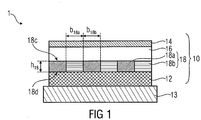
- FIG. 1 shows in particular a layer arrangement 10 of the light emission device 1 which is applied to a substrate 13.
- FIG. The layered arrangement 10 includes a first electrode layer 12 and a second electrode layer 14, both of which include a conductive material such as aluminum. Between the two electrode layers 12 and 14 is a light-emitting layer 16 made of an organic material. This light-emitting layer is designed as a layer stack with a number of individual organic layers. An intermediate layer 18 with an optical lattice structure is provided between the first electrode layer 12 and the light-emitting layer 16 .
- the intermediate layer 18 has an optical lattice structure, which is implemented in this exemplary embodiment by means of first partial lattice regions 18a and second partial lattice regions 18b.
- the grid sections 18a and 18b have different refractive indices and are arranged periodically with a period length which corresponds to the sum of the lateral widths b 18a and b 18b of the partial grating regions 18a and 18b.
- the lateral widths b 18a and b 18b of the partial lattice regions 18a and 18b are the same, with the partial lattice regions 18a and 18b also being able to have different widths b 18a and b 18b , so that the optical properties of the intermediate layer 18 depend on the lattice structure in each area of application are adjustable or selectable.
- the intermediate layer 18 and thus also the partial lattice regions 18a and 18b have a constant layer thickness h 18 between the first and second main surfaces 18c and 18d.
- the substrate 13, on which the electrode layer 12 and thus the layer arrangement 10 is arranged has, for example, opaque silicon or transparent glass. The functioning of this exemplary embodiment is explained in more detail below.
- the emitted light or light modes are directed or aligned in the intermediate layer 18 by means of the optical lattice structure. This alignment of the light modes takes place due to diffraction at the optical grating structure or at the grating sections 18a and 18b, which have different refractive indices, for example.
- the first partial lattice regions 18a are made of doped amorphous silicon and the second partial lattice regions 18b are made of silicon oxide and therefore have different material properties.
- a current flow between the first electrode layer 12 and the second electrode layer 14 through the light-emitting layer 16 is made possible by the intermediate layer 18 being conductive at least in regions between the first and second main surfaces 18c and 18d, because the lattice subregions 18a are made of the conductive material doped amorphous silicon are.
- the light-emitting layer 16 is arranged on the ideally planar surface, namely the first main surface 18c. Since an ideally planar surface cannot be produced for manufacturing reasons, a tolerance range is defined which, on the one hand, meets the requirements with regard to the planarity of the organic layer 16 and on the other hand, can be produced in terms of manufacturing technology.
- the tolerance range defined in the exemplary embodiments according to the invention indicates unevenness of the first main surface 18c in a range of less than +/-20 nm, ie the maximum deviation of a point on the first main surface 18c in the area of the optical lattice structure from the ideal planar one plane is 20 nm in a first direction (towards light-emitting layer 16) or in a second, opposite direction (towards first electrode layer 12). It is noted that larger bumps may be permissible outside the area of the optical lattice structure of the intermediate layer 18 or outside the light-emitting areas of the organic layer 16, since bumps in these areas have a negligible influence on the resulting electrical and optical properties.
- the tolerance value of +/-20 nm is based on the fact that typically the electrical properties of the organic, light-emitting layer 16 are not significantly affected by unevenness within this tolerance range, and due to the fact that typical planarization processes surfaces with a maximum surface unevenness or roughness of less than +/-20 nm.
- the background to the surface unevenness is that with planarization processes, such as chemical-mechanical polishing (CMP), process-related surface unevenness or roughness remain after the grinding process.
- CMP chemical-mechanical polishing
- one of the two partial lattice regions 18a or 18b serves as a stop layer or etch stop layer.
- the intermediate layer 18 which has the first and second partial lattice regions 18a and 18b, since the partial lattice regions 18a and 18b have different material properties that affect the planarization.
- the main surface 18c is planar within a tolerance range of +/-20 nm, +/-10 nm or +/-5 nm is.
- Figure 2a shows the exemplary embodiment according to the invention of a light-emitting device in which the organic light-emitting layer 16 is designed as a layer stack.
- Figure 2b illustrates the dependence of the light extraction efficiency on the layer thickness h 18 of the intermediate layer 18.
- Figure 2c shows the dependence of the light extraction efficiency on the period length and layer thickness of one of the organic layers (HTL layer) of the layer stack.
- Figure 2a shows an exemplary embodiment of a phosphorescent light-emitting device (OLED) that can emit light with a green spectral component.
- the first electrode layer 12 which is referred to as the anode, has aluminum with a layer thickness of 200 nm (eg 180-240 nm).
- the light-emitting layer 16 is implemented by means of a layer stack made up of five individual layers.
- the second single layer is an electron blocking layer 16b (EBL) and comprises 2,2',7,7'-tetrakis-(N,N-diphenylamino)-9,9'-spirobifluorene (Spiro-TAD).
- EML emitting layer
- TCTA 4,4',4"-tris(N-carbazolyl)-triphenylamine
- TPBI 2,2',2"-(1,3,5-benzenetriyl)-tris[1-phenyl- 1>H-benzimidazole]
- the electron blocking layer 16b and the hole transporting layer 16a have a layer thickness of 10 nm (eg 5-15 nm), for example.
- the intermediate layer 18 has at least two materials for forming a linear, optical lattice structure, namely doped amorphous silicon as the first partial lattice regions 18a and silicon oxide as the second partial lattice regions 18b.
- the resulting functionality of the in Figure 2a The light emission device shown basically corresponds to that in 1 illustrated functionality, wherein the light-emitting device shown can emit light with a green spectral component. It is pointed out that light-emitting devices with other organic materials in the organic layers can emit other spectral components. Different parameters that influence the light extraction efficiency are explained below. In general, it can be stated that the period length b 18a +b 18b of the optical grating structure depends on the wavelength of the light to be emitted or is selected accordingly. Therefore, the period length is set to the wavelength of the light to be emitted in a region-wise manner, so that the period length is in a range from 0.2 to 5.0 times the wavelength.
- a period length of the optical lattice structure of, for example, 800 nm (eg 700-900 nm) is optimal for the light emission device with the green spectral component of the light to be emitted according to this exemplary embodiment.
- a maximum of the decoupling efficiency can be achieved, for example, if a layer thickness of the ETL layer of 205 nm (e.g. 180 - 230 nm) is selected and if the layer thickness of the HTL layer is correspondingly reduced to 40 nm (e.g. 30 - 65 nm) is determined.
- Figure 2b shows an example of a diagram of the light coupling-out efficiency of the light-emitting device with the green spectral component of the light to be emitted as a function of the layer thickness h 18 of the intermediate layer 18 with a graph 41 that was determined using a numerical simulation.
- a maximum light extraction efficiency is at a layer thickness h 18 of 60 nm (e.g. between 50-65 nm) and a minimum light extraction efficiency at a layer thickness h 18 of 20 nm
- the layer thickness h 18 is set to 60 nm.
- the outcoupling efficiency of the described embodiment is 27%, which is a 35% increase over the 20% outcoupling efficiency of a configuration without an optical grating structure.
- the layer thickness h 18 of the intermediate layer 18, which typically has a value between 5 and 1000 nm, depends on the frequency of the emitted light and is preferably constant so that the optical properties can be maintained over the entire width of the optical lattice structure are the same.
- Figure 2c shows an example of the simulation result of the light extraction efficiency when the period length is varied as a function of the layer thickness of the HTL layer 16a of the organic layer stack of the light-emitting device, which can emit light with a green spectral component.
- the period length is plotted against the layer thickness of the HTL layer 16a, with the different height lines representing or clarifying the light decoupling efficiency. It can be seen that in a region 43 the light outcoupling efficiency is comparatively high.
- the region 43 extends over a period length of between 550 and 1000 nm and a layer thickness of the HTL layer 16a between 30 and 65 nm, with an absolute maximum (cf.
- marked region 45 being approximately at a period length of 800 nm and a layer thickness of 40nm.
- the interdependent parameters period length and layer thickness of the HTL layer 16a in the in Figure 2a shown embodiment according to the maximum light extraction efficiency (see. Marked area 45) set.
- the optical properties of the intermediate layer are adjusted via further parameters, which is explained in more detail below.
- the different refractive indices of the first and second partial grating regions 18a and 18b result from the different material properties and/or the different Materials of the grid portions 18a and 18b.
- the refractive indices of the partial grating regions 18a and 18b are mutually dependent, depending on the refractive indices of the other layers of the light-emitting device and depending on the wavelength of the light to be emitted.
- the materials or material properties of the first and/or second partial lattice regions 18a or 18b can preferably differ from the material or the material properties of the first electrode layer 12 in order to avoid interfaces that have different refractive indices between the first electrode layer 12 and the first or second partial lattice regions 18a or 18b and thus set the optical properties.
- Another parameter that influences the optical properties of the intermediate layer 18 is the absorption length of the grating sections, which are also set depending on the wavelength of the light to be emitted, so that the absorption length at the emitted wavelength of the light is at least 50 nm.
- the optical lattice structure itself has a further influence on the outcoupling efficiency, which can correspond, for example, to an oblique, right-angled, right-angle-centered, hexagonal or square Bravais lattice or a quasi-crystal in order to outcouple the bound light modes efficiently and at the correct angle.
- 3 14 shows a light emitting device 24 according to another unclaimed comparative example.
- the light emission device 24 has an additional (optional) lateral charge transport layer 26 made of a conductive material, which is arranged between the intermediate layer 18 and the light emitting layer 16 .
- the lateral transport layer 26 is applied to the first planar main surface 18c of the intermediate layer 18 and, like the intermediate layer 18 , has a planar main surface assigned to the light-emitting layer 16 .
- the light emission device 24 basically corresponds to the light emission device 1 in terms of functionality 1 .
- the lateral charge transport layer 26 is applied to the planar first main surface 18c of the intermediate layer 18 and serves to ensure a current flow that is as constant as possible over the surface or a current density distribution that is as homogeneous as possible between the first and second electrode layers 12 and 14 through the organic, light-emitting layer 16 over the to ensure the entire active width of the organic layer 16 or a pixel or sub-pixel of the organic layer 16 .
- the background to this is to eliminate possible effects that arise as a result of the fact that the intermediate layer 18 is only conductive in certain areas, for example in one of the first or second partial lattice regions 18a or 18b.
- the typical charge transport lengths correspond to the lateral widths b 18a and b 18b of the lattice portions 18a and 18b. These are common much smaller than the active width of the organic layer, which determine the charge transport lengths of the electrode layer 12. A lower conductivity is therefore sufficient for the lateral charge transport layer 26 in comparison to the electrode layer 12 .
- the lateral charge transport layer 26 is made of a thin conductive, preferably transparent material such as amorphous silicon. Alternatively, still other conductive materials, such as indium tin oxide or another transparent conductive oxide, preferably with long absorption lengths, can be used.
- FIG. 12 shows a light-emitting device 28 according to a further exemplary embodiment, which is opposite to the light-emitting device 1.
- FIG 1 additionally has an (optional) spacer layer 30 between the intermediate layer 18 and the first electrode layer 12 .
- the functionality of the light-emitting device 28 corresponds to that of the light-emitting device 1.
- the spacer layer 30 serves to optimize the position of the intermediate layer 18 within the resonator, i.e. within the layer arrangement of the electrode layers 12 and 14.
- the layer thickness of the spacer layer 30 is adapted for optimization.
- the spacer layer 30 differs from the electrode layer 12 in terms of its conductivity.
- the spacer layer 30 is used only for vertical current transport, not for the lateral distribution of charge carriers over the entire active area, so that a lower conductivity is sufficient in comparison to the electrode layer 12 .
- the spacer layer 30 can be made of a doped semiconductor such as amorphous silicon or of transparent and conductive metal oxide (TCO), for example, and can preferably have a long absorption length.
- TCO transparent and conductive metal oxide
- figure 5 12 shows a light emission device 32 according to a further comparative example not claimed, in which the intermediate layer with the lattice structures is designed as an intermediate layer stack 18 which has two intermediate layers 18_1 and 18_2.
- the two intermediate layers 18_1 and 18_2 each have an optical lattice structure.
- the layer stack can also have a lateral charge transport layer 26_2 and spacer layers 30_1 and 30_2.
- the light emission device 32 comprises the substrate 13 on which the first electrode layer 12 is arranged.
- the light-emitting layer 16 is arranged between the first electrode layer 12 and the second electrode layer 14 .
- the two intermediate layers 18 1 and 18 2 are located between this light-emitting layer 16 and the first electrode layer 12.
- the first intermediate layer 18_1 arranged closer to the light-emitting layer 16 has first partial grating regions 18a_1 and second partial grating regions 18b_1 of the optical lattice structure.
- the second intermediate layer 18_2 arranged closer to the first electrode layer 12 analogously has first lattice subregions 18a_2 and second lattice subregions 18b_2.
- a further lateral charge transport layer 26_2 is provided on a first main surface 18c_2 of the intermediate layer 18_2 facing the light-emitting layer 16 and a further spacer layer 30_2 is provided on the second main surface 18d_2 facing the first electrode layer 12.
- This comparative example is useful to understand an embodiment without lateral charge transport layer 26_1.
- the light emission device 32 corresponds to the previously mentioned exemplary embodiments, the additional intermediate layer 18_2 with its optical lattice structure being arranged parallel to the intermediate layer 18_1 in order to overlay the effects of a plurality of optical lattice structures. Therefore, the intermediate layer 18_2 can have different lattice properties, such as a different period length, compared to the intermediate layer 18_1. In this way, on the one hand, the outcoupling for several colors can be optimized and, on the other hand, it is possible to selectively outcouple light in several directions at the same time.
- the (optional) lateral charge transport layers 26_1 and 26_2 serve to ensure the lateral transport of charge carriers over the width to of the non-conductive partial lattice regions 18a_1 or 18b_1 or 18a_2 or 18b_2.
- the (optional) spacer layers 30_1 and 30_2 serve to optimize the position of the intermediate layers 18_1 and 18_2 in the layer arrangement.
- Figure 6a shows the initial state of the method 100 for producing the light-emitting device 1.
- a first method step 110 the substrate 13 is provided and the first electrode layer 12 is applied to it.
- a first lattice structure base layer 18a_Basis is applied to the electrode layer 12, from which first lattice partial regions 18a are subsequently formed.
- CVD chemical vapor deposition
- Figure 6b 12 illustrates the subsequent step 120 of patterning the first lattice structure base layer 18a_base.
- the illustration shows the already structured lattice structure base layer, so that these form the first, spaced lattice subregions 18a, as well as exposed intermediate regions 40.
- the lattice structure base layer 18a _Basis or SiO 2 layer is structured to first, spaced lattice subregions 18a and to obtain exposed intermediate regions 40.
- the SiO 2 layer can be coated with a photoresist, which is then structured by photolithographic processes. This structure can then be transferred into the SiO 2 layer by reactive ion etching (RIE).
- RIE reactive ion etching
- Figure 6c shows the step 130 of applying a second lattice structure base layer 18b_Basis to the first, spaced apart lattice subregions 18a and the exposed intermediate regions 40.
- a second lattice structure base layer 18b_Basis made of doped amorphous silicon (a-Si) is applied to the first, spaced apart lattice subregions 18a and the exposed intermediate regions 40, for example by means of chemical vapor deposition.
- a-Si doped amorphous silicon
- FIG. 14 shows the next step 140 of planarizing the second lattice structure base layer 18b _Base, so that second lattice subregions 18b arise. At least the second lattice structure base layer is then planarized in order to obtain the planarized intermediate layer with the optical lattice structure.
- the second lattice structure base layer 18b_basis is polished back down to the first (grown) lattice subregions 18a by means of a chemical-mechanical planarization process (CMP).
- CMP chemical-mechanical planarization process
- Figure 6e shows the final step of the manufacturing method to illustrate the last steps 150 of applying the light-emitting layer 16 and the second electrode layer 14.
- the light-emitting layer 16 which can have a plurality of individual layers, for example, is arranged on the intermediate layer 18, before the second electrode layer 14 is deposited on the light-emitting layer 16.
- the manufacturing method described above can include the step of arranging the lateral charge transport layer 26 after the step of producing the planarized intermediate layer 18 or after the step of planarizing the intermediate layer 18 (before the step of arranging the light-emitting layer 16 on the intermediate layer 18).
- the manufacturing method can include the step of arranging the spacer layer 30 on the electrode 12 before creating the intermediate layer 18 .
- a light-emitting device 32 can be used in accordance with the figure 5 shown embodiment are produced, in which case the step of producing the intermediate layer is carried out once for the intermediate layer 18_1 and once for the intermediate layer 18_2.
- the layer arrangement can be divided into pixels and/or subpixels.
- the light-emitting device By subdividing the pixels, it is possible to use the light-emitting device as a display. By dividing pixels into sub-pixels that can each represent one of the three primary colors, for example, it is possible for the pixel to represent different colors by mixing the three primary colors with different intensities.
- the light emission device can be driven either actively or passively. With active control, an integrated circuit is arranged on the substrate, which selectively controls the pixels and provides the power supply for them. In the case of passive control, the light-emitting device with a plurality of pixels is controlled from the outside via a matrix and is supplied with current. In the passive embodiment, an integrated circuit for driving the pixels can also be located on the same substrate next to the light emitting device or externally.
- the layer arrangement of the light-emitting device can have further light-emitting layers.
- different color representations can be realized in one area if, for example, three different-colored light-emitting layers are arranged one on top of the other.
- a light emitting device may include the spacer layer 30 .
- the intermediate layer 18 can have further grating regions besides the first and second grating regions with further refractive indices.
- the light emission device 32 can have an intermediate layer stack 18 with further intermediate layers 18_1, 18_2, 18_3, ... and 18_n.
- the exemplary embodiments of the light emission device described can be used both as a top-emitting OLED (TOLED) and as a bottom-emitting OLED (BOLED) and as a transparent OLED, depending on the material properties of the substrate 13 and the electrode layers 12 and 14 .
- TOLED top-emitting OLED
- BOLED bottom-emitting OLED
- transparent OLED depending on the material properties of the substrate 13 and the electrode layers 12 and 14 .
- an opaque substrate 13, a reflective electrode layer 12 and a transparent electrode layer 14 are used for TOLEDs, in contrast to BOLEDs.
- the structure of the light emission device can be flat and/or divided into pixels or subpixels and the emitted light can therefore be radiated flat and/or in pixels or subpixels.
Landscapes
- Physics & Mathematics (AREA)
- Optics & Photonics (AREA)
- Electroluminescent Light Sources (AREA)
Claims (10)
- Dispositif d'émission de lumière (1, 24, 28, 32), aux caractéristiques suivantes:un substrat (13); etun aménagement de couches (10) appliqué sur le substrat (13) avec une première couche d'électrodes (12) en un matériau conducteur disposée sur le substrat (13), avec une deuxième couche d'électrodes (14) en un matériau conducteur, avec au moins une couche électroluminescente (16) en un matériau organique qui est disposée entre la première couche d'électrodes (12) et la deuxième couche d'électrodes (14) et est réalisée en forme de pile de couches organiques (16), et avec au moins une couche intermédiaire (18) présentant une structure de grille optique et qui est disposée entre la pile de couches organiques (16) et la première couche d'électrodes (12),dans lequel une première surface principale (18c) de la couche intermédiaire (18) fait face à la pile de couches organiques (16) et la première surface principale (18c) de la couche intermédiaire (18) est réalisée plane au moins dans la zone de structure de grille optique dans une plage de tolérance conditionnée par la fabrication, dans lequel, dans la zone électroluminescente de la couche intermédiaire (18), la plage de tolérance dans la zone des irrégularités de la première surface principale (18c) se situe dans une plage de moins de +/- 20 nm ou de préférence de +/- 10 nm; et dans lequel la couche intermédiaire (18) est conductrice au moins par zones entre la première surface principale (18c) et une deuxième surface principale (18d) de cette dernière,dans lequel la couche intermédiaire (18) comporte des premières et deuxièmes zones de grille partielles (18a, 18b), dans lequel les premières et deuxièmes zones de grille partielles (18a, 18b) sont disposées l'une à côté de l'autre et dans lequel les premières et deuxièmes zones de grille partielles (18a, 18b) présentent une même hauteur de couche, pour former ainsi une épaisseur de couche constante (h18) de la couche intermédiaire (18), et dans lequel la première zone de grille partielle (18a) présente un silicium amorphe dopé et la deuxième zone de grille partielle (18b) présente un oxyde de silicium;dans lequel la pile de couches organiques (16) présente une couche de transport à trous (16a), une couche de blocage d'électrons (16b), une couche électroluminescente 16c), une couche de blocage de trous (16d) et une couche de transport d'électrons (16e); etdans lequel la première surface principale (18c) de la couche intermédiaire (18) et la pile de couches organiques (16) sont directement adjacentes l'une à l'autre.
- Dispositif d'émission de lumière (1, 24, 28, 32) selon la revendication 1, dans lequel la longueur de période (b18a + b18b) de la structure de grille optique, au moins par zones, est réglée à une longueur d'onde de la lumière à émettre par la couche électroluminescente (16).
- Dispositif d'émission de lumière (1, 24, 28, 32) selon l'une des revendications précédentes, dans lequel la longueur de période (b18a + b18b) de la structure de grille de la couche intermédiaire (18) se situe dans une plage de 0,2 à 5,0 de la longueur d'onde de la lumière à émettre par la couche électroluminescente (16).
- Dispositif d'émission de lumière (1, 24, 28, 32) selon l'une des revendications précédentes, dans lequel l'aménagement de couches (10) présente en outre une couche d'espacement conductrice homogène (30) entre la couche intermédiaire (18) et la première couche d'électrodes (12).
- Dispositif d'émission de lumière (1, 24, 28, 32) selon l'une des revendications précédentes, dans lequel la structure de grille optique de la couche intermédiaire (18) correspond à une grille de Bravais oblique, à angle droit, centré à angle droit, hexagonal ou carré ou est réalisée en forme d'un quasi-cristal.
- Dispositif d'émission de lumière (1, 24, 28, 32) selon l'une des revendications précédentes, dans lequel l'épaisseur de couche (h18) de la couche intermédiaire (18) est constante dans une autre plage de tolérance et est inférieure à 1000 nm.
- Dispositif d'émission de lumière (1, 24, 28, 32) selon l'une des revendications précédentes, dans lequel l'aménagement de couches (10) est subdivisé en pixels et/ou sous-pixels qui peuvent être commandés de manière sélective, passive ou active au moyen d'un circuit intégré.
- Dispositif d'émission de lumière (1, 24, 28, 32) selon l'une des revendications précédentes, dans lequel la couche intermédiaire (18) et la première et la deuxième couche d'électrodes (12, 14) présentent des matériaux conducteurs différents.
- Dispositif d'émission de lumière (1, 24, 28, 32) selon l'une des revendications précédentes, dans lequel l'aménagement de couches (10) présente une autre couche intermédiaire (18_2) avec une autre structure de grille optique qui est disposée entre la première couche intermédiaire (18_1) et la première couche d'électrodes (12),
dans lequel une première surface principale (18c_2) de l'autre couche intermédiaire (18_2) fait face à la couche électroluminescente (16) et la première surface principale (18c_2) de l'autre couche intermédiaire (18_2) est réalisée plane au moins dans la zone de la structure de grille optique dans une plage de tolérance, et dans lequel l'autre couche intermédiaire est conductrice au moins par zones entre la première surface principale (18c_2) et une deuxième surface principale (18d_2) de cette dernière. - Procédé (100) de fabrication d'un dispositif d'émission de lumière (1, 24, 28, 32) selon l'une des revendications précédentes avec un aménagement de couches (10), aux étapes suivantes consistant à:prévoir (110) le substrat (13);disposer (110) la première couche d'électrodes (12) sur le substrat (13);générer (110, 120, 130, 140) la couche intermédiaire aplanie (18) présentant la structure de grille optique sur la couche d'électrodes (12);disposer (150) la pile de couches organiques (16) sur la couche intermédiaire (18); etdisposer (150) la deuxième couche d'électrodes (14) sur la pile de couches organiques (16),dans lequel l'étape consistant à générer la couche intermédiaire présente les étapes suivantes consistant à:appliquer (110) la première couche de base à structure de grille (18a_Basis) sur la couche d'électrodes (12);structurer (120) la première couche de base à structure de grille (18a_Basis) pour obtenir des premières zones de grille partielles distantes l'une de l'autre (18a) et des zones intermédiaires exposées (40);appliquer (130) une deuxième couche de base à structure de grille (18b_Basis) sur les premières zones de grille partielles distantes l'une de l'autre (18a) et les zones intermédiaires exposées (40); etaplanir (140) au moins la deuxième couche de base à structure de grille (18b_Basis) pour obtenir la couche intermédiaire aplanie (18) à la structure de grille optique.
Priority Applications (6)
| Application Number | Priority Date | Filing Date | Title |
|---|---|---|---|
| EP11172129.6A EP2541637B1 (fr) | 2011-06-30 | 2011-06-30 | Dispositif d'émission de lumière électroluminescente doté d'une structure de grille optique et son procédé de fabrication |
| KR1020137034687A KR20140032458A (ko) | 2011-06-30 | 2012-06-29 | 격자 구조를 포함하는 전자발광 발광 장치, 및 이의 생산을 위한 방법 |
| JP2014517734A JP2014518439A (ja) | 2011-06-30 | 2012-06-29 | 光学的格子構造を含むエレクトロルミネッセンス発光素子およびその製造方法。 |
| CN201280032714.XA CN103636024B (zh) | 2011-06-30 | 2012-06-29 | 包括光学晶格结构的电致发光器件及其制造方法 |
| PCT/EP2012/062711 WO2013001063A1 (fr) | 2011-06-30 | 2012-06-29 | Système d'émission de lumière à électroluminescence comportant une structure à réseau optique ainsi que son procédé de fabrication |
| US14/135,654 US20140103328A1 (en) | 2011-06-30 | 2013-12-20 | Electroluminescent light emission device comprising an optical lattice structure and method for manufacturing same |
Applications Claiming Priority (1)
| Application Number | Priority Date | Filing Date | Title |
|---|---|---|---|
| EP11172129.6A EP2541637B1 (fr) | 2011-06-30 | 2011-06-30 | Dispositif d'émission de lumière électroluminescente doté d'une structure de grille optique et son procédé de fabrication |
Publications (2)
| Publication Number | Publication Date |
|---|---|
| EP2541637A1 EP2541637A1 (fr) | 2013-01-02 |
| EP2541637B1 true EP2541637B1 (fr) | 2022-01-12 |
Family
ID=46397288
Family Applications (1)
| Application Number | Title | Priority Date | Filing Date |
|---|---|---|---|
| EP11172129.6A Active EP2541637B1 (fr) | 2011-06-30 | 2011-06-30 | Dispositif d'émission de lumière électroluminescente doté d'une structure de grille optique et son procédé de fabrication |
Country Status (6)
| Country | Link |
|---|---|
| US (1) | US20140103328A1 (fr) |
| EP (1) | EP2541637B1 (fr) |
| JP (1) | JP2014518439A (fr) |
| KR (1) | KR20140032458A (fr) |
| CN (1) | CN103636024B (fr) |
| WO (1) | WO2013001063A1 (fr) |
Families Citing this family (7)
| Publication number | Priority date | Publication date | Assignee | Title |
|---|---|---|---|---|
| US9159955B1 (en) * | 2014-04-04 | 2015-10-13 | Grantwood Limited | Method and apparatus for patterning an organic device |
| DE102014106549B4 (de) * | 2014-05-09 | 2023-10-19 | Pictiva Displays International Limited | Organisches Licht emittierendes Bauelement |
| KR102207914B1 (ko) * | 2014-10-10 | 2021-01-27 | 삼성디스플레이 주식회사 | 유기 발광 표시 장치 |
| US10115000B2 (en) | 2015-12-11 | 2018-10-30 | Synaptics Incorporated | Method and system for optical imaging using patterned illumination |
| TWI703744B (zh) * | 2016-04-08 | 2020-09-01 | 晶元光電股份有限公司 | 發光元件 |
| CN108878674A (zh) | 2017-05-11 | 2018-11-23 | 京东方科技集团股份有限公司 | 显示基板及其制作方法、显示装置 |
| WO2023156923A1 (fr) * | 2022-02-16 | 2023-08-24 | Oti Lumionics Inc. | Dispositif à semi-conducteur stratifié ayant un revêtement conducteur commun sur des discontinuités longitudinales |
Citations (4)
| Publication number | Priority date | Publication date | Assignee | Title |
|---|---|---|---|---|
| US20020080493A1 (en) * | 2000-12-21 | 2002-06-27 | Rung-Ywan Tsai | Polarization-independent ultra-narrow band pass filters |
| US20050275994A1 (en) * | 2004-05-28 | 2005-12-15 | Novatek Microelectronic Co. | Transient voltage detecting circuit |
| US20100141612A1 (en) * | 2006-11-24 | 2010-06-10 | Comissariat A L'energie Atomique | Electrode of a light-emitting device of the oled type |
| EP2339658A2 (fr) * | 2009-12-23 | 2011-06-29 | Commissariat à l'Énergie Atomique et aux Énergies Alternatives | Procédé de fabrication d'une électrode a nanostructures métallique et diélectrique pour le filtrage coloré dans une OLED et procédé de fabrication d'une OLED |
Family Cites Families (21)
| Publication number | Priority date | Publication date | Assignee | Title |
|---|---|---|---|---|
| JP3832088B2 (ja) * | 1998-04-23 | 2006-10-11 | 松下電器産業株式会社 | 有機発光素子 |
| US6704335B1 (en) * | 1998-12-17 | 2004-03-09 | Seiko Epson Corporation | Light-emitting device |
| JP2002056988A (ja) * | 2000-08-10 | 2002-02-22 | Seiko Epson Corp | 発光装置 |
| KR100581850B1 (ko) * | 2002-02-27 | 2006-05-22 | 삼성에스디아이 주식회사 | 유기 전계 발광 표시 장치와 그 제조 방법 |
| US7038373B2 (en) | 2002-07-16 | 2006-05-02 | Eastman Kodak Company | Organic light emitting diode display |
| KR20050121691A (ko) * | 2003-03-25 | 2005-12-27 | 교또 다이가꾸 | 발광 소자 및 유기 일렉트로루미네선스 발광 소자 |
| US6911674B2 (en) * | 2003-04-16 | 2005-06-28 | Zeolux Corporation | Feedback and coupling structures and methods |
| JP4220305B2 (ja) * | 2003-05-22 | 2009-02-04 | 三星エスディアイ株式会社 | 有機エレクトロルミネセンス素子 |
| KR100852110B1 (ko) | 2004-06-26 | 2008-08-13 | 삼성에스디아이 주식회사 | 유기 전계 발광 소자 및 그 제조 방법 |
| KR100615257B1 (ko) * | 2004-10-05 | 2006-08-25 | 삼성에스디아이 주식회사 | 유기 전계 발광 표시 장치 및 이의 제조 방법 |
| JP4511440B2 (ja) | 2004-10-05 | 2010-07-28 | 三星モバイルディスプレイ株式會社 | 有機発光素子及び有機発光素子の製造方法 |
| KR100730121B1 (ko) * | 2004-11-29 | 2007-06-19 | 삼성에스디아이 주식회사 | 유기 전계 발광 소자 및 그 제조 방법 |
| US20090039764A1 (en) * | 2005-03-17 | 2009-02-12 | Cho Kyung Sang | Quantum Dot Light-Emitting Diode Comprising Inorganic Electron Transport Layer |
| JP4517910B2 (ja) * | 2005-03-24 | 2010-08-04 | コニカミノルタホールディングス株式会社 | 有機エレクトロルミネッセンス素子ならびにこれを備えた照明装置および表示装置 |
| WO2006134218A1 (fr) | 2005-06-15 | 2006-12-21 | Braggone Oy | Structure d'un dispositif optique |
| JP2007258526A (ja) * | 2006-03-24 | 2007-10-04 | Konica Minolta Holdings Inc | 有機エレクトロルミネッセンス素子、及び有機エレクトロルミネッセンスディスプレイ |
| US20070241326A1 (en) | 2006-04-18 | 2007-10-18 | Samsung Electronics Co., Ltd. | Organic light emitting diode display and manufacturing method thereof |
| GB0622998D0 (en) | 2006-11-17 | 2006-12-27 | Microemissive Displays Ltd | Colour optoelectronic device |
| US20090015142A1 (en) | 2007-07-13 | 2009-01-15 | 3M Innovative Properties Company | Light extraction film for organic light emitting diode display devices |
| KR100873517B1 (ko) * | 2007-11-21 | 2008-12-15 | 한국기계연구원 | 유기발광소자 |
| JP5471162B2 (ja) * | 2009-08-25 | 2014-04-16 | 住友化学株式会社 | 有機エレクトロルミネッセンス素子 |
-
2011
- 2011-06-30 EP EP11172129.6A patent/EP2541637B1/fr active Active
-
2012
- 2012-06-29 JP JP2014517734A patent/JP2014518439A/ja active Pending
- 2012-06-29 WO PCT/EP2012/062711 patent/WO2013001063A1/fr active Application Filing
- 2012-06-29 CN CN201280032714.XA patent/CN103636024B/zh not_active Expired - Fee Related
- 2012-06-29 KR KR1020137034687A patent/KR20140032458A/ko not_active Application Discontinuation
-
2013
- 2013-12-20 US US14/135,654 patent/US20140103328A1/en not_active Abandoned
Patent Citations (4)
| Publication number | Priority date | Publication date | Assignee | Title |
|---|---|---|---|---|
| US20020080493A1 (en) * | 2000-12-21 | 2002-06-27 | Rung-Ywan Tsai | Polarization-independent ultra-narrow band pass filters |
| US20050275994A1 (en) * | 2004-05-28 | 2005-12-15 | Novatek Microelectronic Co. | Transient voltage detecting circuit |
| US20100141612A1 (en) * | 2006-11-24 | 2010-06-10 | Comissariat A L'energie Atomique | Electrode of a light-emitting device of the oled type |
| EP2339658A2 (fr) * | 2009-12-23 | 2011-06-29 | Commissariat à l'Énergie Atomique et aux Énergies Alternatives | Procédé de fabrication d'une électrode a nanostructures métallique et diélectrique pour le filtrage coloré dans une OLED et procédé de fabrication d'une OLED |
Also Published As
| Publication number | Publication date |
|---|---|
| WO2013001063A1 (fr) | 2013-01-03 |
| JP2014518439A (ja) | 2014-07-28 |
| CN103636024B (zh) | 2017-10-13 |
| US20140103328A1 (en) | 2014-04-17 |
| EP2541637A1 (fr) | 2013-01-02 |
| KR20140032458A (ko) | 2014-03-14 |
| CN103636024A (zh) | 2014-03-12 |
Similar Documents
| Publication | Publication Date | Title |
|---|---|---|
| EP2541637B1 (fr) | Dispositif d'émission de lumière électroluminescente doté d'une structure de grille optique et son procédé de fabrication | |
| EP1713136B1 (fr) | Dispositif pour diode électroluminescente organique et méthode de sa fabrication | |
| EP1410450B1 (fr) | Composant electroluminescent a couches organiques | |
| EP1982362B1 (fr) | Composant optoélectronique organique | |
| EP2193559B1 (fr) | Dispositif émettant un rayonnement | |
| EP1739765A1 (fr) | Diode organoluminescent et empilement des OLEDs | |
| DE102012111877A1 (de) | Weisse tandem-organische lichtemittierende vorrichtung | |
| EP2619815B1 (fr) | Modulation de porteur de charge pour une syntonisation de la couleur et de la luminosité dans des diodes électroluminescentes organiques | |
| DE102014106634B4 (de) | Beleuchtungsvorrichtung, Verfahren zum Herstellen einer Beleuchtungsvorrichtung | |
| DE102005043546A1 (de) | Organische EL-Anzeige | |
| DE112014002460B4 (de) | Organisches elektrolumineszierendes Element | |
| DE102004041371A1 (de) | Aktiv-Matrix-Display auf der Basis organischer Leuchtdioden mit erhöhtem Füllfaktor | |
| DE102012216265A1 (de) | Weisse organische Licht-emittierende Vorrichtung | |
| DE112013000629T5 (de) | Organisches EL-Element und Verfahren zum Herstellen desselben | |
| DE112012001410T5 (de) | Organisches Elektrolumineszenzelement | |
| WO2013135765A1 (fr) | Élément électronique avec couche-barrière contre l'humidité | |
| DE102014115562A1 (de) | Optoelektronische komponente, verfahren zur herstellung einer optoelektronischen komponente und verfahren zum bearbeiten eines trägers | |
| DE112012001417T5 (de) | Weißes Licht emittierendes organisches Elektrolumineszenzelement und weißes Licht emittierende organische Elektrolumineszenzplatte | |
| WO2015059278A1 (fr) | Composant optoélectronique et procédé de fabrication d'un composant optoélectronique | |
| DE102012203583A1 (de) | Organisches Licht emittierendes Bauelement | |
| DE102011079048A1 (de) | Lichtemittierende bauelemente und verfahren zum herstellen eines lichtemittierenden bauelements | |
| DE102011079063A1 (de) | Lichtemittierendes Bauelement und Verfahren zum Herstellen eines lichtemittierenden Bauelements | |
| EP1788647B1 (fr) | Dispositif électroluminescent | |
| CN104810481A (zh) | 有机发光元件 | |
| EP2936583B1 (fr) | Procédé de fabrication d'un composant électroluminescent organique |
Legal Events
| Date | Code | Title | Description |
|---|---|---|---|
| PUAI | Public reference made under article 153(3) epc to a published international application that has entered the european phase |
Free format text: ORIGINAL CODE: 0009012 |
|
| AK | Designated contracting states |
Kind code of ref document: A1 Designated state(s): AL AT BE BG CH CY CZ DE DK EE ES FI FR GB GR HR HU IE IS IT LI LT LU LV MC MK MT NL NO PL PT RO RS SE SI SK SM TR |
|
| AX | Request for extension of the european patent |
Extension state: BA ME |
|
| 17P | Request for examination filed |
Effective date: 20130610 |
|
| RBV | Designated contracting states (corrected) |
Designated state(s): AL AT BE BG CH CY CZ DE DK EE ES FI FR GB GR HR HU IE IS IT LI LT LU LV MC MK MT NL NO PL PT RO RS SE SI SK SM TR |
|
| STAA | Information on the status of an ep patent application or granted ep patent |
Free format text: STATUS: EXAMINATION IS IN PROGRESS |
|
| 17Q | First examination report despatched |
Effective date: 20190409 |
|
| STAA | Information on the status of an ep patent application or granted ep patent |
Free format text: STATUS: EXAMINATION IS IN PROGRESS |
|
| GRAP | Despatch of communication of intention to grant a patent |
Free format text: ORIGINAL CODE: EPIDOSNIGR1 |
|
| STAA | Information on the status of an ep patent application or granted ep patent |
Free format text: STATUS: GRANT OF PATENT IS INTENDED |
|
| INTG | Intention to grant announced |
Effective date: 20210727 |
|
| GRAS | Grant fee paid |
Free format text: ORIGINAL CODE: EPIDOSNIGR3 |
|
| GRAA | (expected) grant |
Free format text: ORIGINAL CODE: 0009210 |
|
| STAA | Information on the status of an ep patent application or granted ep patent |
Free format text: STATUS: THE PATENT HAS BEEN GRANTED |
|
| AK | Designated contracting states |
Kind code of ref document: B1 Designated state(s): AL AT BE BG CH CY CZ DE DK EE ES FI FR GB GR HR HU IE IS IT LI LT LU LV MC MK MT NL NO PL PT RO RS SE SI SK SM TR |
|
| REG | Reference to a national code |
Ref country code: GB Ref legal event code: FG4D Free format text: NOT ENGLISH |
|
| REG | Reference to a national code |
Ref country code: CH Ref legal event code: EP |
|
| REG | Reference to a national code |
Ref country code: DE Ref legal event code: R096 Ref document number: 502011017288 Country of ref document: DE |
|
| REG | Reference to a national code |
Ref country code: IE Ref legal event code: FG4D Free format text: LANGUAGE OF EP DOCUMENT: GERMAN |
|
| REG | Reference to a national code |
Ref country code: AT Ref legal event code: REF Ref document number: 1462958 Country of ref document: AT Kind code of ref document: T Effective date: 20220215 |
|
| RAP4 | Party data changed (patent owner data changed or rights of a patent transferred) |
Owner name: FRAUNHOFER-GESELLSCHAFT ZUR FOERDERUNG DER ANGEWANDTEN FORSCHUNG E.V. |
|
| REG | Reference to a national code |
Ref country code: LT Ref legal event code: MG9D |
|
| REG | Reference to a national code |
Ref country code: NL Ref legal event code: MP Effective date: 20220112 |
|
| PG25 | Lapsed in a contracting state [announced via postgrant information from national office to epo] |
Ref country code: NL Free format text: LAPSE BECAUSE OF FAILURE TO SUBMIT A TRANSLATION OF THE DESCRIPTION OR TO PAY THE FEE WITHIN THE PRESCRIBED TIME-LIMIT Effective date: 20220112 |
|
| PG25 | Lapsed in a contracting state [announced via postgrant information from national office to epo] |
Ref country code: SE Free format text: LAPSE BECAUSE OF FAILURE TO SUBMIT A TRANSLATION OF THE DESCRIPTION OR TO PAY THE FEE WITHIN THE PRESCRIBED TIME-LIMIT Effective date: 20220112 Ref country code: RS Free format text: LAPSE BECAUSE OF FAILURE TO SUBMIT A TRANSLATION OF THE DESCRIPTION OR TO PAY THE FEE WITHIN THE PRESCRIBED TIME-LIMIT Effective date: 20220112 Ref country code: PT Free format text: LAPSE BECAUSE OF FAILURE TO SUBMIT A TRANSLATION OF THE DESCRIPTION OR TO PAY THE FEE WITHIN THE PRESCRIBED TIME-LIMIT Effective date: 20220512 Ref country code: NO Free format text: LAPSE BECAUSE OF FAILURE TO SUBMIT A TRANSLATION OF THE DESCRIPTION OR TO PAY THE FEE WITHIN THE PRESCRIBED TIME-LIMIT Effective date: 20220412 Ref country code: LT Free format text: LAPSE BECAUSE OF FAILURE TO SUBMIT A TRANSLATION OF THE DESCRIPTION OR TO PAY THE FEE WITHIN THE PRESCRIBED TIME-LIMIT Effective date: 20220112 Ref country code: HR Free format text: LAPSE BECAUSE OF FAILURE TO SUBMIT A TRANSLATION OF THE DESCRIPTION OR TO PAY THE FEE WITHIN THE PRESCRIBED TIME-LIMIT Effective date: 20220112 Ref country code: ES Free format text: LAPSE BECAUSE OF FAILURE TO SUBMIT A TRANSLATION OF THE DESCRIPTION OR TO PAY THE FEE WITHIN THE PRESCRIBED TIME-LIMIT Effective date: 20220112 Ref country code: BG Free format text: LAPSE BECAUSE OF FAILURE TO SUBMIT A TRANSLATION OF THE DESCRIPTION OR TO PAY THE FEE WITHIN THE PRESCRIBED TIME-LIMIT Effective date: 20220412 |
|
| PG25 | Lapsed in a contracting state [announced via postgrant information from national office to epo] |
Ref country code: PL Free format text: LAPSE BECAUSE OF FAILURE TO SUBMIT A TRANSLATION OF THE DESCRIPTION OR TO PAY THE FEE WITHIN THE PRESCRIBED TIME-LIMIT Effective date: 20220112 Ref country code: LV Free format text: LAPSE BECAUSE OF FAILURE TO SUBMIT A TRANSLATION OF THE DESCRIPTION OR TO PAY THE FEE WITHIN THE PRESCRIBED TIME-LIMIT Effective date: 20220112 Ref country code: GR Free format text: LAPSE BECAUSE OF FAILURE TO SUBMIT A TRANSLATION OF THE DESCRIPTION OR TO PAY THE FEE WITHIN THE PRESCRIBED TIME-LIMIT Effective date: 20220413 Ref country code: FI Free format text: LAPSE BECAUSE OF FAILURE TO SUBMIT A TRANSLATION OF THE DESCRIPTION OR TO PAY THE FEE WITHIN THE PRESCRIBED TIME-LIMIT Effective date: 20220112 |
|
| PG25 | Lapsed in a contracting state [announced via postgrant information from national office to epo] |
Ref country code: IS Free format text: LAPSE BECAUSE OF FAILURE TO SUBMIT A TRANSLATION OF THE DESCRIPTION OR TO PAY THE FEE WITHIN THE PRESCRIBED TIME-LIMIT Effective date: 20220512 |
|
| REG | Reference to a national code |
Ref country code: DE Ref legal event code: R097 Ref document number: 502011017288 Country of ref document: DE |
|
| PG25 | Lapsed in a contracting state [announced via postgrant information from national office to epo] |
Ref country code: SM Free format text: LAPSE BECAUSE OF FAILURE TO SUBMIT A TRANSLATION OF THE DESCRIPTION OR TO PAY THE FEE WITHIN THE PRESCRIBED TIME-LIMIT Effective date: 20220112 Ref country code: SK Free format text: LAPSE BECAUSE OF FAILURE TO SUBMIT A TRANSLATION OF THE DESCRIPTION OR TO PAY THE FEE WITHIN THE PRESCRIBED TIME-LIMIT Effective date: 20220112 Ref country code: RO Free format text: LAPSE BECAUSE OF FAILURE TO SUBMIT A TRANSLATION OF THE DESCRIPTION OR TO PAY THE FEE WITHIN THE PRESCRIBED TIME-LIMIT Effective date: 20220112 Ref country code: EE Free format text: LAPSE BECAUSE OF FAILURE TO SUBMIT A TRANSLATION OF THE DESCRIPTION OR TO PAY THE FEE WITHIN THE PRESCRIBED TIME-LIMIT Effective date: 20220112 Ref country code: DK Free format text: LAPSE BECAUSE OF FAILURE TO SUBMIT A TRANSLATION OF THE DESCRIPTION OR TO PAY THE FEE WITHIN THE PRESCRIBED TIME-LIMIT Effective date: 20220112 Ref country code: CZ Free format text: LAPSE BECAUSE OF FAILURE TO SUBMIT A TRANSLATION OF THE DESCRIPTION OR TO PAY THE FEE WITHIN THE PRESCRIBED TIME-LIMIT Effective date: 20220112 |
|
| PLBE | No opposition filed within time limit |
Free format text: ORIGINAL CODE: 0009261 |
|
| STAA | Information on the status of an ep patent application or granted ep patent |
Free format text: STATUS: NO OPPOSITION FILED WITHIN TIME LIMIT |
|
| REG | Reference to a national code |
Ref country code: DE Ref legal event code: R079 Ref document number: 502011017288 Country of ref document: DE Free format text: PREVIOUS MAIN CLASS: H01L0051520000 Ipc: H10K0050800000 |
|
| PG25 | Lapsed in a contracting state [announced via postgrant information from national office to epo] |
Ref country code: AL Free format text: LAPSE BECAUSE OF FAILURE TO SUBMIT A TRANSLATION OF THE DESCRIPTION OR TO PAY THE FEE WITHIN THE PRESCRIBED TIME-LIMIT Effective date: 20220112 |
|
| 26N | No opposition filed |
Effective date: 20221013 |
|
| PG25 | Lapsed in a contracting state [announced via postgrant information from national office to epo] |
Ref country code: MC Free format text: LAPSE BECAUSE OF FAILURE TO SUBMIT A TRANSLATION OF THE DESCRIPTION OR TO PAY THE FEE WITHIN THE PRESCRIBED TIME-LIMIT Effective date: 20220112 |
|
| REG | Reference to a national code |
Ref country code: CH Ref legal event code: PL |
|
| REG | Reference to a national code |
Ref country code: BE Ref legal event code: MM Effective date: 20220630 |
|
| PG25 | Lapsed in a contracting state [announced via postgrant information from national office to epo] |
Ref country code: SI Free format text: LAPSE BECAUSE OF FAILURE TO SUBMIT A TRANSLATION OF THE DESCRIPTION OR TO PAY THE FEE WITHIN THE PRESCRIBED TIME-LIMIT Effective date: 20220112 |
|
| PG25 | Lapsed in a contracting state [announced via postgrant information from national office to epo] |
Ref country code: LU Free format text: LAPSE BECAUSE OF NON-PAYMENT OF DUE FEES Effective date: 20220630 Ref country code: LI Free format text: LAPSE BECAUSE OF NON-PAYMENT OF DUE FEES Effective date: 20220630 Ref country code: IE Free format text: LAPSE BECAUSE OF NON-PAYMENT OF DUE FEES Effective date: 20220630 Ref country code: CH Free format text: LAPSE BECAUSE OF NON-PAYMENT OF DUE FEES Effective date: 20220630 |
|
| PG25 | Lapsed in a contracting state [announced via postgrant information from national office to epo] |
Ref country code: BE Free format text: LAPSE BECAUSE OF NON-PAYMENT OF DUE FEES Effective date: 20220630 |
|
| P01 | Opt-out of the competence of the unified patent court (upc) registered |
Effective date: 20230524 |
|
| PG25 | Lapsed in a contracting state [announced via postgrant information from national office to epo] |
Ref country code: IT Free format text: LAPSE BECAUSE OF FAILURE TO SUBMIT A TRANSLATION OF THE DESCRIPTION OR TO PAY THE FEE WITHIN THE PRESCRIBED TIME-LIMIT Effective date: 20220112 |
|
| REG | Reference to a national code |
Ref country code: AT Ref legal event code: MM01 Ref document number: 1462958 Country of ref document: AT Kind code of ref document: T Effective date: 20220630 |
|
| PG25 | Lapsed in a contracting state [announced via postgrant information from national office to epo] |
Ref country code: AT Free format text: LAPSE BECAUSE OF NON-PAYMENT OF DUE FEES Effective date: 20220630 |
|
| PG25 | Lapsed in a contracting state [announced via postgrant information from national office to epo] |
Ref country code: HU Free format text: LAPSE BECAUSE OF FAILURE TO SUBMIT A TRANSLATION OF THE DESCRIPTION OR TO PAY THE FEE WITHIN THE PRESCRIBED TIME-LIMIT; INVALID AB INITIO Effective date: 20110630 |
|
| PG25 | Lapsed in a contracting state [announced via postgrant information from national office to epo] |
Ref country code: MK Free format text: LAPSE BECAUSE OF FAILURE TO SUBMIT A TRANSLATION OF THE DESCRIPTION OR TO PAY THE FEE WITHIN THE PRESCRIBED TIME-LIMIT Effective date: 20220112 Ref country code: CY Free format text: LAPSE BECAUSE OF FAILURE TO SUBMIT A TRANSLATION OF THE DESCRIPTION OR TO PAY THE FEE WITHIN THE PRESCRIBED TIME-LIMIT Effective date: 20220112 |
|
| PGFP | Annual fee paid to national office [announced via postgrant information from national office to epo] |
Ref country code: GB Payment date: 20240620 Year of fee payment: 14 |
|
| PGFP | Annual fee paid to national office [announced via postgrant information from national office to epo] |
Ref country code: DE Payment date: 20240617 Year of fee payment: 14 |
|
| PGFP | Annual fee paid to national office [announced via postgrant information from national office to epo] |
Ref country code: FR Payment date: 20240617 Year of fee payment: 14 |