EP2538664B1 - Imaging apparatus and method of driving the same - Google Patents
Imaging apparatus and method of driving the same Download PDFInfo
- Publication number
- EP2538664B1 EP2538664B1 EP12169574.6A EP12169574A EP2538664B1 EP 2538664 B1 EP2538664 B1 EP 2538664B1 EP 12169574 A EP12169574 A EP 12169574A EP 2538664 B1 EP2538664 B1 EP 2538664B1
- Authority
- EP
- European Patent Office
- Prior art keywords
- signal
- circuit
- ramp
- comparing
- comparison
- Prior art date
- Legal status (The legal status is an assumption and is not a legal conclusion. Google has not performed a legal analysis and makes no representation as to the accuracy of the status listed.)
- Active
Links
Images


Classifications
-
- H—ELECTRICITY
- H04—ELECTRIC COMMUNICATION TECHNIQUE
- H04N—PICTORIAL COMMUNICATION, e.g. TELEVISION
- H04N25/00—Circuitry of solid-state image sensors [SSIS]; Control thereof
- H04N25/60—Noise processing, e.g. detecting, correcting, reducing or removing noise
-
- H—ELECTRICITY
- H04—ELECTRIC COMMUNICATION TECHNIQUE
- H04N—PICTORIAL COMMUNICATION, e.g. TELEVISION
- H04N25/00—Circuitry of solid-state image sensors [SSIS]; Control thereof
- H04N25/70—SSIS architectures; Circuits associated therewith
- H04N25/71—Charge-coupled device [CCD] sensors; Charge-transfer registers specially adapted for CCD sensors
- H04N25/745—Circuitry for generating timing or clock signals
-
- H—ELECTRICITY
- H03—ELECTRONIC CIRCUITRY
- H03M—CODING; DECODING; CODE CONVERSION IN GENERAL
- H03M1/00—Analogue/digital conversion; Digital/analogue conversion
- H03M1/12—Analogue/digital converters
- H03M1/50—Analogue/digital converters with intermediate conversion to time interval
- H03M1/56—Input signal compared with linear ramp
-
- H—ELECTRICITY
- H04—ELECTRIC COMMUNICATION TECHNIQUE
- H04N—PICTORIAL COMMUNICATION, e.g. TELEVISION
- H04N25/00—Circuitry of solid-state image sensors [SSIS]; Control thereof
- H04N25/60—Noise processing, e.g. detecting, correcting, reducing or removing noise
- H04N25/616—Noise processing, e.g. detecting, correcting, reducing or removing noise involving a correlated sampling function, e.g. correlated double sampling [CDS] or triple sampling
-
- H—ELECTRICITY
- H04—ELECTRIC COMMUNICATION TECHNIQUE
- H04N—PICTORIAL COMMUNICATION, e.g. TELEVISION
- H04N25/00—Circuitry of solid-state image sensors [SSIS]; Control thereof
- H04N25/70—SSIS architectures; Circuits associated therewith
- H04N25/71—Charge-coupled device [CCD] sensors; Charge-transfer registers specially adapted for CCD sensors
- H04N25/75—Circuitry for providing, modifying or processing image signals from the pixel array
-
- H—ELECTRICITY
- H04—ELECTRIC COMMUNICATION TECHNIQUE
- H04N—PICTORIAL COMMUNICATION, e.g. TELEVISION
- H04N25/00—Circuitry of solid-state image sensors [SSIS]; Control thereof
- H04N25/70—SSIS architectures; Circuits associated therewith
- H04N25/76—Addressed sensors, e.g. MOS or CMOS sensors
Definitions
- the present invention relates to an imaging apparatus and a method of driving the same.
- Digital cameras using a CMOS image sensor as an imaging device are known.
- An imaging device that applies analog to digital (AD) conversion to a pixel signal is known enabling signal readout at high speed.
- One of the AD conversion techniques has been known in which a comparator compares a pixel signal with a time-dependent reference signal (ramp signal) and acquires an AD-converted data according to the signal amplitude.
- the imaging device thus including an AD converter is expected to achieve high speed reading and high resolution.
- the technique of Japanese Patent Application Laid-Open No. 2007-281987 utilizes a plurality of comparators. Accordingly, there is a problem in that the response speeds are different according to variation in manufacturing elements configuring the comparators, causing an error in the AD-converted data. Furthermore, there is difficulty in increasing a circuit area and power consumption.
- the document US 2011/0037868 A1 discloses a solid-state image sensing element which includes a pixel array portion in which a plurality of pixels each including a photoelectric converter are arranged two-dimensionally, and readout circuits which read out analog pixel signals from the pixel array portion by column, and in which each of the readout circuits includes an A/D conversion circuit which converts the analog pixel signal from the pixel array portion into a digital pixel signal, and the A/D conversion circuit performs A/D conversion by comparing, by a comparison unit, a signal level of the analog pixel signal from the pixel array portion with a temporally changing reference level.
- a frequency band characteristic of the comparison unit is switched in accordance with the signal level of the analog pixel signal from the pixel array portion.
- the document US 2008/0192127 A1 discloses a solid-state imaging device which includes a reference-signal generating unit that generates plural kinds of reference signals for converting an analog pixel signal into digital data, a reference-signal selecting unit that selects any one of the plural kinds of reference signals, a comparing unit that compares the pixel signal and the selected reference signal, and a count unit that performs count processing in parallel with comparison processing in the comparing unit and stores a count value at a point when the comparison processing is completed.
- the count unit decides digital data of the pixel signal in a 1 LSB step by storing a count value at a point when the comparison processing is completed for any one of the plural kinds of reference signals and correcting the stored count value on the basis of results of the comparison processing for respective remaining reference signals of the plural kinds of reference signals.
- an imaging apparatus and a method of driving the same as specified in the claims.
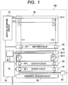
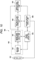
- FIG. 1 is a schematic configurational diagram of an imaging device 100 of a first embodiment of the present invention.
- the imaging device 100 is a CMOS image sensor, photoelectric-converts a subject image formed by received light and outputs the electric signal as a digital signal.
- the imaging device 100 includes a pixel unit 10, a vertical scanning circuit 15, an amplifying unit 20, a ramp signal generating circuit (reference signal generating circuit) 25, a comparator unit 30, a counter unit 40, a memory unit 50, an output circuit 60, a horizontal scanning circuit 65 and a timing generation circuit (TG) 70.
- the pixel unit 10 includes pixels 10-1 arranged in a two-dimensional matrix. The pixel 10-1 outputs a pixel signal by photoelectric conversion.
- the vertical scanning circuit 15 outputs drive pulses X-1, X-2,... to the pixel unit 10.
- the amplifying unit 20 amplifies the pixel signal from the pixel unit 10.
- the ramp signal generating circuit 25 generates a time-dependent ramp signal (reference signal) as a comparison signal for the pixel signal.
- the comparator unit 30 compares the pixel signal amplified by the amplifying unit 20 with the ramp signal.
- the counter unit 40 counts until the comparator unit 30 outputs a comparison result.
- the memory unit 50 holds a count data of the counter unit 40, and performs bit-shifting and operation on the held data.
- the horizontal scanning circuit 65 transfers a data from memory unit 50 to the output circuit 60 by horizontal scanning.
- the timing generation circuit 70 controls timing of the circuit blocks.
- the pixels 10-1 are arranged in an area of the pixel unit 10. However, FIG. 1 schematically illustrates only four pixels.
- the rows of pixels 10-1 are sequentially driven by respective drive pulses X-1, X-2 from the vertical scanning circuit 15.
- a reset signal (comparison signal) of each pixel 10-1 and an effective signal as a photoelectric conversion signal are guided to amplifying unit 20 via vertical output lines V-1 to V-n.
- Circuits, from the amplifying unit 20 to the memory unit 50, are provided for the respective vertical output lines V-1 to V-n.
- Each amplifying circuit 20-1 of the amplifying unit 20 may only have a function of simply amplifying the signal from the pixel 10-1.
- the circuit may have a CDS processing function that performs a difference process between the effective signal and the reset signal.
- the CDS process is performed in an input section of the comparator unit 30.
- the amplifying unit 20 is not a mandatory. However, amplification has an advantageous effect of reducing impact of noise caused in the comparator unit 30.
- the comparator unit 30 includes a comparing circuit 30-1 from the amplifying unit 20 according to the pixel column, and a selecting circuit 30-2 that selects one of the ramp signals.
- the comparator unit 30 determines whether the amplitude of the pixel signal from the amplifying circuit 20-1 is larger or smaller than a reference comparison signal set in consideration of the SN ratio of the pixel signal, selects a ramp signal to be compared with the pixel signal according to the result, and performs a comparison process.
- Each comparing circuit 30-1 outputs an inversion signal, which is a comparison result compared with the selected one ramp signal, according to the determined result of the input signal amplitude.
- the comparator unit 30 compares the pixel signal with the ramp signal.
- the counter unit 40 counts counter clocks from the leading edge of the ramp signal to inversion of the output signal.
- the count result is held as an AD-converted data in a memory circuit 50-1 of the memory unit 50.
- the memory circuit 50-1 performs one of bit-shifting and operation on the AD-converted data of the reset signal and the AD-converted data of the effective signal, thereby increasing the number of bits, and transfers the processed data to the output circuit 60 according to scanning pulses from the horizontal scanning circuit 65.
- the imaging device 100 causes the one comparing circuit 30-1 to perform comparison with the ramp signal according to the amplitude of the pixel signal. Accordingly, the device exerts an advantageous effect that can acquire a multiple-bit AD-converted data by an AD conversion process concerning a small number of bits.
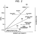
- FIG. 2 is a diagram illustrating the SN ratio of the pixel signal for describing an operational principle of the imaging device 100 in FIG. 1 .
- the abscissa of FIG. 2 represents the incident light quantity onto the pixel 10-1.
- the ordinate indicates LOG representation of the signal level photoelectric-converted according to the incident light quantity.
- a broken line 202 represents an optical shot noise. As known well, the amount of noise is represented as ⁇ N.
- the broken line 203 represents pixel system noise after CDS (including noise due to the amplifier but excluding noise due to AD conversion).
- the SN ratio that is a ratio between the signal level of 1 V and the pixel system noise of 0.2 mV is 74 dB.
- AD conversion supporting this SN ratio requires a resolution about 14 bits in consideration of the quantization bit error. The higher the resolution is, the more the counter time increases. Accordingly, a certain AD conversion time is required. In the imaging device, the speed of signal readout is reduced. Resultantly, high speed imaging cannot be performed.
- This embodiment thus achieves high speed readout by reducing the number of AD-converted bits. For instance, in the case of assuming that a large amplitude signal level is 1 V, the optical shot noise 202 is large. Accordingly, provided that the large amplitude signal level is 10000 charges and the optical shot noise is 100, the SN ratio is 40 dB. In the case of assuming that a small amplitude signal level is 10 mV, the SN ratio is 20 dB. That is, any point of the signal level is only required to have a resolution for securing an SN ratio of a little over 40 dB.
- FIG. 2 discusses 10-bit AD conversion with classification into a large amplitude signal AD(H) and a small amplitude signal AD(L) at a boundary of 62.5 mV, which is 1/16 (corresponding to four bits) of a signal of 1 V.
- a chain double-dashed line 204 represents a resolution of AD conversion for a signal amplitude of 1 V.
- An alternate long and short dashed line 205 represents a resolution of AD conversion for a signal amplitude of 62.5 mV.
- both the two types of AD conversion have an AD conversion accuracy of 10 bits, the representation indicates that the AD resolution is small even in consideration of a quantization error in the optical shot noise 202.
- a 10-bit AD converter can acquire an AD-converted data having 14-bit accuracy, by bit-shifting on the two AD-converted data.
- Conversion for a large amplitude signal and a small amplitude signal is according to 10 bits.
- a 14-bit resolution can be achieved for a signal range of 1 V, by combining both types having such a relationship.
- conversion of a large amplitude signal is discussed.
- a small amplitude signal up to the boundary of 62.5 mV is AD-converted using a ramp signal having a slope of 1/16 of a ramp signal for the large amplitude signal.
- the resolution 205 of the AD conversion of a small amplitude signal is 1/16 of the resolution 204 of the AD conversion of a large amplitude signal.
- the resolution of 10-bit AD conversion for the signal amplitude of 62.5 mV is 62.5 mV/1024 ⁇ 0.0612 mV.
- the resolution of 0.0612 mV is sufficiently small with respect to the value of 0.2 mV of the pixel system noise 203.
- the signal of 62.5 mV as the boundary can be dealt with as a large amplitude signal or a small amplitude signal.
- FIG. 3 is a diagram illustrating ramp signals according to this embodiment.
- FIG. 3 illustrates a slope that represents temporal change of a ramp signal.
- a first ramp signal (first reference signal) VH is used for the signal amplitudes of 62.5 mV and higher in FIG. 2 .
- a second ramp signal (second reference signal) VL is used for signals less than 62.5 mV.
- the second ramp signal has a smaller slope (time-dependent change rate) than the first ramp signal VH.
- the slope ratio of ramp signals VH and VL is 16. With the slope ratio of 16, the resolution is increased by four bits. Both the AD converting circuits adopt 10-bit conversion and identical maximum conversion time. Accordingly, the counter clock has the same clock frequency. With a slope ratio of 8, the resolution is increased by three bits. In FIG.
- the AD-converted resolution for the small amplitude signal is sufficiently smaller than system noise. Accordingly, the resolution may be nine bits.
- the maximum clock frequency fmax of the counter is assigned to 10-bit AD conversion, to reduce conversion time.
- the counter clocks of the 9-bit AD converting circuit is 1/2 x fmax.
- the slope ratio of the ramp signal and the resolution of the AD converting circuit are determined based on the number of saturated charges of the pixel, the system noise and the resolution required for the imaging device 100.
- the slope ratio of ramp signals VH and VL having different slopes may be a multiple of two.
- the counter unit 40 may count the ramp signals VH and VL using the counter clock having the same frequency. Instead, the count may be according to counter clocks having different frequencies.
- FIG. 4 is a block diagram of the AD converting unit illustrating connection of the comparing circuit 30-1 to input and output circuits according to the first embodiment of the present invention. Blocks having the same functions as the blocks in FIG. 1 are assigned with the same symbols. The description is omitted.
- the AD converting unit can convert a photoelectric-converted analog signal into a digital signal at high speed.
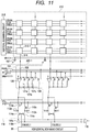
- FIG. 11 is a diagram illustrating an example of configurations of the pixel unit 210 and the amplifying circuit 220-1 in the imaging device, where the comparator unit 30, the counter unit 40 and the memory unit 50 are omitted.
- a CDS circuit 119 is provided after the amplifying circuit 220-1.
- the pixel unit 210 includes pixels 210-1 arranged in multiple columns and multiple rows.
- signals output from pixels at odd columns from the left are read by reading circuits arranged below the pixel unit 210.
- signals output from pixels at even columns from the left are read by reading circuits, not illustrated, arranged above the pixel unit 210.
- the reading circuits are alternately arranged. Accordingly, an area for two column of the pixel unit 210 can be utilized for the layout of the reading circuit.
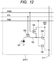
- FIG. 12 is a circuit diagram of one pixel 210-1.
- a transfer switch 102 is driven by a transfer pulse PTX.
- a reset switch 103 is driven by a reset pulse PRES.
- a row selection switch 105 is driven by a row selection pulse PSEL.
- Representation PTX is for PTX1 to n (n is the number of rows).
- Representation PRES is for PRES1 to n.
- Representation PSEL is for PSEL1 to n.
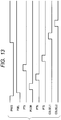
- FIG. 13 is a timing chart illustrating an example of an operation of the imaging device illustrated in FIG. 11 .
- the imaging device is exposed to light for a set exposure time before a reading operation.
- Photo carriers are accumulated in a photodiode 101.
- the PRES1, PTX1 and PSEL1 output from the vertical scanning circuit 215 select a row to be driven.
- the pixel reset pulse PRES is changed from the high level to the low level to cancel the reset of the gate electrode of an amplifier MOSFET 104.
- a potential corresponding to cancellation of the reset is held in a floating diffusion region FD connected to the gate electrode.
- the row selection pulse PSEL becomes the high level
- an output corresponding to the potential of the floating diffusion region FD appears at the vertical output line V-1 by a source follower circuit formed by the amplifier MOSFET 104 and a constant current source 107.
- a clamp pulse PC0R is activated to the high level.
- a clamp switch 109 is turned on, a variable amplifier 131 becomes in a voltage-follower state, and the electrode of a clamp capacitor 108 on a column amplifier side has a voltage substantially identical to a voltage VREF. Subsequently, the clamp pulse PC0R is inactivated from the high level to the low level, and the output on the vertical output line V-1 is clamped.
- an accumulated pulse PTN is activated to the high level, and an offset signal of the amplifying circuit 220-1 is stored in a holding capacitor 112n via a transfer gate 110n.
- a transfer pulse PTX is activated to the high level.
- the transfer switch 102 becomes the high level for a certain time, and the photo carriers accumulated in the photodiode 101 are transferred to the gate electrode of the amplifier MOSFET 104.
- the transferred charges are electrons.
- the absolute value of the amount of transferred charges is Q and the capacitance of the floating diffusion region FD is CFD, the gate potential decreases by Q/CFD. The potential of the vertical output line V-1 is changed accordingly.
- Equation (1) the amount of change ⁇ Vvl of the potential Vvl of the vertical output line V-1 due to transfer of charges from the photodiode 101 to the floating diffusion unit FD is represented according to Equation (1).
- ⁇ Vvl ⁇ Q ⁇ Gsf / CFD
- Vct VREF + Q ⁇ Gsf / CFD ⁇ C 0 / Cf
- the clamp capacitor 108 has a capacitance C0.
- Cf 1 pF.
- Cf 0.5 pF.
- Cf 0.25 pF.
- the voltage gains represented as -C0/Cf are -1-fold, -2-fold and -4-fold.
- any of the feedback capacitors 121a to 121c changes the feedback ratio determined by the partial pressure ratio of Cf and C0, thereby allowing the voltage gain to be switched.
- the negative sign of the voltage gain represents that the circuit is an inverting amplification circuit.
- the transfer pulse PTX becomes the low level
- the accumulated pulse PTS becomes the high level.
- the level of the output from the amplifying circuit 220-1 at the time is accumulated in a holding capacitor 112s via a transfer gate 110s.
- scanning pulses COLSEL1 and COLSEL2,... generated by the horizontal scanning circuit 65 sequentially turn on column selection switches 114s and 114n.
- the signals accumulated in the holding capacitor 112s are output to a horizontal output line 116s according to the sequence of the columns.
- the signals accumulated in the holding capacitor 112n are output to the horizontal output line 116n in the sequence of the columns.
- the signal pairs of the columns are sequentially output to the horizontal output lines 116s and 116n.
- a difference processor 118 outputs the differences of the signal pairs output to the horizontal output lines 116s and 116n. Accordingly, noise components included in the signals held in the holding capacitor 112s can be reduced.
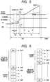
- FIG. 5 is a timing chart illustrating a method of driving the imaging device 100 of this embodiment, and particularly, is a timing chart of the AD converting unit in FIG. 4 .
- a time Tad is AD conversion time of the N signal and the S signal of the analog signal Va read from the pixels.
- a time Tdata is an AD-converted data transfer time.
- a time Td is an N signal AD conversion time from the pixels, and a ramp signal VR is a comparison signal therefor.
- a time Tj is a signal level determination time for the S signal.
- a comparison signal VREF is a comparison signal therefore.
- a time Tu is an S signal AD conversion time.
- a ramp signal VH (or ramp signal VL) is a comparison signal therefor.
- An output signal Va of the amplifying circuit 20-1 mainly takes the illustrated N and S signal levels, and is guided into an input terminal of the comparing circuit 30-1.
- a ramp signal VRAMP which is a comparison signal for signal Va, is input into the other input terminal of the comparing circuit 30-1.
- the N signal in the following description corresponds to a signal sampled by a signal PTN in FIG. 13 , in the case where the CDS circuit is provided before the comparator unit 30. On the other hand, in the case with no CDS circuit, the signal corresponds to a signal output to the vertical signal line in response to reset of the floating diffusion unit.
- the S signal in the following description corresponds to a signal sampled by a signal PTS in FIG. 13 , in the case where the CDS circuit is provided before the comparator unit 30.
- the signal corresponds to a signal output to the vertical signal line output in response to transfer of charges caused in the photodiode to the floating diffusion unit.
- the ramp signal generating circuit 25 generates a ramp signal VH/comparison signal VREF and a ramp signal VL/ramp signal VR, under control of a control signal CNT2 of the timing generation circuit 70.
- the ramp signal VH is for higher-order bits having a large slope.
- the ramp signal VL is for lower-order bits having a small slope.
- the comparison signal VREF is a reference comparison signal for determining the S signal level.
- the ramp signal VR is for comparison with the N signal.
- the comparing circuit 30-1 compares the N signal with the ramp signal VR in the N signal AD conversion time Td. In a time Tr, the ramp signal VR starts to change and the magnitude relation with the N signal is inverted.
- the counter circuit 40-1 counts, in the time Tr.
- the memory circuit 50-1 holds the counting value as the N signal data.
- the ramp signal VR has the same slope as the ramp signal VL. According to the same slope, an N signal AD-converted data with high resolution can be acquired.
- the comparing circuit 30-1 compares the signal levels of the S signal and the comparison signal VREF with each other, in S signal level determination time Tj.
- the comparing circuit 30-1 outputs to the selecting circuit 30-2 a high level selection signal SEL representing a comparison result in which the S signal is higher than the comparison signal VREF, in the S signal level determination time Tj.
- the selecting circuit 30-2 selects the ramp signal VH with the large slope in the S signal AD conversion time Tu, and outputs the signal to the comparing circuit 30-1.
- the comparing circuit 30-1 compares the S signal with the ramp signal VH, the counter circuit 40-1 performs a counting operation in time Ts in which the magnitude relation of the signals are inverted.
- the memory circuit 50-1 holds the counting value as the S signal AD-converted data.
- the selecting circuit 30-2 selects the ramp signal VL with the small slope as the ramp signal.
- the comparing circuit 30-1 compares the S signal with the ramp signal VL.
- the selecting circuit 30-2 selects the one of the ramp signals VH and VL having the different slopes, according to the level of the S signal amplified by the amplifying unit 20. That is, the selecting circuit 30-2 sets the time-dependent change rate of the ramp signal according to the level of the S signal based on the pixels.
- the comparing circuit 30-1 compares the ramp signal selected by the selecting circuit 30-2 and the S signal amplified by the amplifying unit 20 with each other.
- the counter circuit 40-1 counts from the time when the ramp signal starts to change to the time when the comparing circuit 30-1 outputs the signal representing inversion of the magnitude relation between the S signal and the ramp signal.
- the ramp signal VR and the ramp signal VL have the same slope, as described above.
- the ramp signal VR is compared with the N signal.
- the N signal also functions as the comparison signal for the S signal, and is therefore required to have high accuracy.
- the ramp signal VR has the same slope as the ramp signal VL for generating the lower-order bits. Accordingly, there is an advantageous effect capable of utilizing the same ramp signal generating circuit 25.
- the counting result of the counter circuit 40-1 is stored in the memory unit 50.
- the memory unit 50 subtracts the N signal AD-converted data from the S signal AD-converted data.
- the subtracted data is transferred from the memory unit 50 to the output circuit 60, under control of the horizontal scanning circuit 65.
- This difference process removes an AD conversion error due to variation in offset of the amplifying circuit 20-1 and variation in response speed of the comparing circuit 30-1.
- the AD-converted data of the S signal having been AD-converted using the ramp signal VL, is subjected to a difference operation with the N signal AD-converted data.
- the S signal AD-converted data which has been AD-converted using the ramp signal VH and has the slope of the ramp signal different from the N signal AD-converted data, is subjected to bit-shifting by four bits and then subjected to a difference operation with the N signal AD-converted data.
- the main factors of variation in potential of the N signal are the N signal when the pixels are reset, the offset of the amplifying circuit 20-1, and a variational component (up to several tens of millivolts) of comparing circuit 30-1 at the initial setting.
- the offset component between the N signal and the amplifying circuit 20-1 is reduced in the CDS process before the comparing circuit 30-1.
- the variational component of the comparing circuit 30-1 may be considered to be the N signal AD-converted data.
- the AD-converted data of the large amplitude signal has 14 bits.
- the four least significant bits (4LSB) is smaller than the optical shot noise 202 ( FIG. 2 ) and can therefore be regarded as a dummy data.
- the gain of the amplifying circuit 20-1 in FIG. 4 is one, provided that the pixel signal from the pixel unit 10 is the signal 201 described with FIG. 2 .
- an imaging system that will be described later with FIG. 10 has sensitivity setting suitable for the imaging environment. For instance, in the case of 16-fold sensitivity setting, the signal level of 62.5 mV in FIG. 2 is amplified to 1 V, and the signal is input into the comparing circuit 30-1. At this time, a resolution of 10-bit AD conversion, which compares the large amplitude signal with the ramp signal VH, is sufficient for the SN ratio required for AD conversion.
- the selecting circuit 30-2 may perform a control so as to select the ramp signal VH according to a control signal CONT1 from the timing generation circuit 70 and to output the signal to the comparing circuit 30-1.
- the SN ratio of the pixel unit 10 is mainly affected by the aperture area of the pixel unit 10.
- the slope ratio of the ramp signal VH and the ramp signal VL and sensitivity setting for selecting the ramp signal VH are changed according to the aperture area.
- FIG. 6 is a diagram illustrating a bit-shifting unit for the AD-converted data of this embodiment.
- the bit-shifting unit in the memory circuit 50-1 performs a bit-shifting process.
- the AD-converted data here is described as a data acquired by subtracting the N signal AD-converted data from the S signal AD-converted data.
- FIG. 6A illustrates a case where the S signal is the reference comparison signal (62.5 mV in this embodiment); the AD-converted data is a comparison result with the ramp signal VH having the large slope.
- the AD-converted data D0 to D9 is subjected to 4-bit-shifting and output as AD-converted data Da4 to Da13.
- FIG. 6B illustrates a case where the S signal is lower than the reference comparison signal; the AD-converted data is a comparison result with the ramp signal VL having the low slope.
- the AD-converted data D0 to D9 are not subjected to bit-shifting, but output, as they are, as AD-converted data Da0 to Da9.
- signal amplitudes of bits to the data Da9 are AD-converted.
- the higher-order bits at and higher than the data Da10 are not at the high level.
- the data Da10 to Da13 are set to the low level.
- the number of types of ramp signals with different slopes may be three or more.
- the bit-shifting unit applies bit-shifting at least to the data D0 to D9 corresponding to the ramp signal with the largest slope.
- This embodiment changes the slope of the ramp signal at the boundary of the amplitude of the S signal of 62.5 mV. Accordingly, in the case where the amplitude of the S signal is 62.5 mV or more, the 10-bit AD-converted data D0 to D9 are subjected to 4-bit-shifting. Thus, 14-bit AD-converted data Da0 to Da13 can be acquired.
- This embodiment has described that switching of the ramp signal is at the signal level of 62.5 mV. However, the level may be one of 65 and 70 mV. That is, any S signal is necessarily compared with one of the ramp signals VH and VL, thereby allowing the AD-converted data to be acquired.
- the optical shot noise 202 and the AD-converted data are different in difference of resolutions from each other.
- the resolution of AD conversion is lower than the optical shot noise 202, which does not cause a problem.
- the switching signal level is not necessarily set to be the AD conversion accuracy or less. The level may have a low accuracy.
- the bit-shifting unit can be provided in the imaging device, at any of sites where the data from the counter unit 40 is stored in the memory unit 50, transferred from the memory unit 50 to the output circuit 60, and output from the output circuit 60 to the outside of the imaging device 100.
- the bit-shifting unit may be provided outside of the imaging device 100 (e.g., in a video signal processing circuit unit 830 in FIG. 10 ). In this case, if a flag data for recognizing the signal determination level (selection signal SEL) for the reference comparison signal is added to the AD-converted data, any bit-shifting method can easily be supported.
- the AD-converted data D0 to D9 output from the counter unit 40 are output together with the flag data representing the level of the S signal.
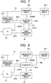
- FIG. 7 is a block diagram of an AD converting unit according to a second embodiment of the present invention.
- the signal level is determined by a signal level determining circuit (selecting circuit) 30-3.
- the ramp signal switching may be determined at a low accuracy. Accordingly, the switching is not necessarily determined by the comparing circuit 30-1. Instead, the switching may be determined by the signal level determining circuit 30-3. In this case, the ramp signal generating circuit 25 outputs the ramp signal VH and the ramp signal VL/ramp signal VR to the selecting circuit 30-2.
- the signal level determining circuit 30-3 When the S signal is higher than the comparison signal VREF, the signal level determining circuit 30-3 outputs a high level determination signal SEL2 to the selecting circuit 30-2, and the selecting circuit 30-2 outputs the ramp signal VH to the comparing circuit 30-1 based on the high level determination signal SEL2.
- the signal level determining circuit 30-3 When the S signal is lower than comparison signal VREF, the signal level determining circuit 30-3 outputs the low level determination signal SEL2 to the selecting circuit 30-2, and the selecting circuit 30-2 outputs the ramp signal VL to the comparing circuit 30-1 based on the low level determination signal SEL2.
- the comparison signal VREF is not necessary for the ramp signal VRAMP of this embodiment. Since the ramp signal generating circuit 25 does not generate the ramp signal VREF, the ramp signal generating circuit 25 can be simplified.
- FIG. 8 is a block diagram of an AD converting unit according to the third embodiment of the present invention.
- the ramp signal generating circuit 25 generates the ramp signal VH and outputs the signal to an attenuator 30-4.
- the attenuator 30-4 attenuates the ramp signal VH generated by the ramp signal generating circuit 25, thereby generating the ramp signals VL and VR having different slopes.
- the attenuator 30-4 outputs one of the ramp signals VH, VL and VR to the comparing circuit 30-1 according to the control signal CONT1 and determination signal SEL2 (or the selection signal SEL).
- the attenuator 30-4 is thus provided, thereby exerting an advantageous effect of reducing the number of wirings from the ramp signal generating circuit 25 to the attenuator 30-4.
- FIG. 9 is a block diagram of a bit number adjusting unit for the AD-converted data of this embodiment.
- the bit number adjusting unit includes output buffers.
- 10-bit AD-converted data D0 to D9 are subject to the bit-shifting into 14-bit AD-converted data Da0 to Da13, thereby achieving high resolution.
- low resolution and low power consumption may be required.
- optical shot noise and system noise are high and the SN ratio of the signal are degraded.
- any of 12 and 10 bits may be adopted as the AD-converted data.
- the output buffers are supplied with a power source voltage Vdd, and buffer and output 14-bit data Da0 to Da13.
- the output buffers for the four least significant bits data Da0 to Da3 are supplied with the power source voltage Vdd by control signals Dcont2 and Dcont4. In the case where the output buffers for the four least significant bits data Da0 to Da3 are not supplied with the power source voltage Vdd by the control signals Dcont2 and Dcont4, the output buffers for the higher-order 10-bit data Da4 to Da13 output 10-bit data Da4 to Da13.
- the output buffers for the lower-2 bit data Da0 and Da1 are not supplied with the power source voltage Vdd by the control signal Dcont2
- the output buffers for the higher order 12-bit data Da2 to Da13 output 12-bit data Da2 to Da13. Accordingly, any of 14, 12 and 10-bit AD-converted data can be output.
- the bit number adjusting unit reduces the number of bits of the data having been subjected to bit-shifting by the bit-shifting unit in FIG. 6 according to the control signals Dcont2 and Dcont4.
- the number of utilization bits and power consumption of the AD-converted data can be controlled by the control signals Dcont2 and Dcont4.
- the number of utilization bits is thus controlled, thereby exerting advantageous effects that reduce the power consumption of the imaging device 100 and the power consumption of the image signal processing of the imaging system in FIG. 10 .
- the number of utilization bits can be controlled according to one of the gains of the amplifying unit 20 and the sensitivity setting of the imaging system in FIG. 10 .
- FIG. 10 is a diagram illustrating an example of the configuration of an imaging system according to a fourth embodiment of the present invention.
- the imaging system 800 includes, for instance, an optical unit 810, the imaging device 100, a video signal processing circuit unit 830, a recording and communicating unit 840, a timing control circuit unit 850, a system control circuit unit 860 and a reproducing and displaying unit 870.
- An imaging apparatus 820 includes the imaging device 100 and the video signal processing circuit unit 830.
- the imaging device 100 used here is the same device illustrated in the embodiments.
- the optical unit 810 which is an optical system such as a lens, forms an image of light from a subject on the pixel unit 10 ( FIG. 1 ) of the imaging device 100 where the pixels are two-dimensionally arranged to form a subject image.
- the imaging device 100 outputs a signal according to the light formed on the pixel unit 10 at the timing based on the signal from the timing control circuit unit 850.
- the signal output from the imaging device 100 is input into the video signal processing circuit unit 830, which is a video signal processor.
- the video signal processing circuit unit 830 performs a signal processing, such as the bit-shifting process in FIG. 6 , on the input signal according to a method defined by the program.
- the signal acquired by the process in the video signal processing circuit unit 830 is transmitted as an image data to the recording and communicating unit 840.
- the recording and communicating unit 840 transmits a signal for forming an image, to the reproducing and displaying unit 870, thereby causing the reproducing and displaying unit 870 to reproduce and display any of a moving image and a still image.
- the recording and communicating unit 840 receives the signal from the video signal processing circuit unit 830, communicates with the system control circuit unit 860, and performs an operation of recording a signal for forming an image on a recording medium, not illustrated.
- the system control circuit unit 860 controls the operation of the imaging system in an integrated manner, and controls driving of the optical unit 810, the timing control circuit unit 850, the recording and communicating unit 840 and the reproducing and displaying unit 870.
- the system control circuit unit 860 includes a storing device, which is for instance a recording medium and not illustrated. A program required for controlling the operation of the imaging system is recorded in the medium.
- the system control circuit unit 860 supplies the imaging system with a signal that, for instance, switches a drive mode in response to an operation of a user. Specific examples include change of rows for reading and resetting, change of the angle of view according to electronic zooming, and shifting of the angle of view for electronic vibration isolation.
- the timing control circuit unit 850 controls driving timing of the imaging device 100 and the video signal processing circuit unit 830, based on control by the system control circuit unit 860 as a control unit.
- the first to fourth embodiments determine whether the signal to be AD-converted has a large or small amplitude, and perform a comparison process using the ramp signal having the slope suitable for the determined signal, thereby acquiring the AD-converted data and achieving the multiple-bit configuration according to the bit-shifting process in FIG. 6 .
- the S signal Under a dark imaging environment, in some exposure conditions, the S signal easily becomes a small amplitude signal. Thus, amplification of the S signal for improvement in sensitivity can be considered.
- the amplifying circuit 20-1 amplifies the signal, thereby allowing the sensitivity to be improved.
- the slope of the ramp signal can be changed to thereby improve the sensitivity as a result.
- the embodiments do not uniquely determine the slope of the ramp signal. Instead, the slope of the ramp signal can be changed according to required improvement in sensitivity. For instance, in the case of doubled improvement in sensitivity, the slope can be controlled to be half.
- the ramp signal whose level is changed linearly with respect to time has been described as the reference signal.
- the signal may have a stepwisely changing slope.
- the imaging apparatus includes: a pixel (10-1) for generating a signal by photoelectric conversion; a comparing circuit (30-1) for comparing a signal based on the pixel with a time-dependent reference signal; a counter circuit (40-1) performing a counting operating until an inversion of a magnitude relation between the signal based on the pixel and the time-dependent reference signal; and a selecting circuit (30-2) for setting a time-dependent change rate of the reference signal, according to a signal level of the signal based on the pixel.
Description
- The present invention relates to an imaging apparatus and a method of driving the same.
- Digital cameras using a CMOS image sensor as an imaging device are known. An imaging device that applies analog to digital (AD) conversion to a pixel signal is known enabling signal readout at high speed. One of the AD conversion techniques has been known in which a comparator compares a pixel signal with a time-dependent reference signal (ramp signal) and acquires an AD-converted data according to the signal amplitude. The imaging device thus including an AD converter is expected to achieve high speed reading and high resolution.
- In consideration of optical shot noise of the pixel signal, only bits enough for achieving the SN ratio are necessary. According to classification into multiple signal levels, high speed readout and high resolution can be achieved by reducing the number of bits. Further, a method of combining comparators and reference signals according to signal amplitudes has been known (e.g., see Japanese Patent Application Laid-Open No.
2007-281987 - The technique of Japanese Patent Application Laid-Open No.
2007-281987 - The document
US 2011/0037868 A1 discloses a solid-state image sensing element which includes a pixel array portion in which a plurality of pixels each including a photoelectric converter are arranged two-dimensionally, and readout circuits which read out analog pixel signals from the pixel array portion by column, and in which each of the readout circuits includes an A/D conversion circuit which converts the analog pixel signal from the pixel array portion into a digital pixel signal, and the A/D conversion circuit performs A/D conversion by comparing, by a comparison unit, a signal level of the analog pixel signal from the pixel array portion with a temporally changing reference level. In such solid-state image sensing element, a frequency band characteristic of the comparison unit is switched in accordance with the signal level of the analog pixel signal from the pixel array portion. - The document
US 2008/0192127 A1 discloses a solid-state imaging device which includes a reference-signal generating unit that generates plural kinds of reference signals for converting an analog pixel signal into digital data, a reference-signal selecting unit that selects any one of the plural kinds of reference signals, a comparing unit that compares the pixel signal and the selected reference signal, and a count unit that performs count processing in parallel with comparison processing in the comparing unit and stores a count value at a point when the comparison processing is completed. The count unit decides digital data of the pixel signal in a 1 LSB step by storing a count value at a point when the comparison processing is completed for any one of the plural kinds of reference signals and correcting the stored count value on the basis of results of the comparison processing for respective remaining reference signals of the plural kinds of reference signals. - According to the present invention, there is provided an imaging apparatus and a method of driving the same, as specified in the claims.
- Further features of the present invention will become apparent from the following description of exemplary embodiments with reference to the attached drawings.
-
-
FIG. 1 is a configurational diagram of an imaging device according to a first embodiment of the present invention. -
FIG. 2 is a diagram illustrating the SN ratio of a pixel signal. -
FIG. 3 is a diagram illustrating ramp signals. -
FIG. 4 is a block diagram of an AD converting unit of the first embodiment of the present invention. -
FIG. 5 is a timing chart of the AD converting unit inFIG. 4 . -
FIG. 6 is a diagram illustrating a bit-shifting unit for the AD-converted data. -
FIG. 7 is a block diagram of an AD converting unit according to a second embodiment of the present invention. -
FIG. 8 is a block diagram of an AD converting unit according to a third embodiment of the present invention. -
FIG. 9 is a block diagram of a bit number adjusting unit for an AD-converted data. -
FIG. 10 is a configurational diagram of an imaging system. -
FIG. 11 is a conceptual diagram illustrating an example of a configuration of the imaging device inFIG. 1 . -
FIG. 12 is an equivalent circuit diagram of a pixel. -
FIG. 13 is a timing chart illustrating an example of an operation of the imaging device illustrated inFIG. 11 . - Preferred embodiments of the present invention will now be described in detail in accordance with the accompanying drawings.
-
FIG. 1 is a schematic configurational diagram of animaging device 100 of a first embodiment of the present invention. Theimaging device 100 is a CMOS image sensor, photoelectric-converts a subject image formed by received light and outputs the electric signal as a digital signal. Theimaging device 100 includes apixel unit 10, avertical scanning circuit 15, an amplifying unit 20, a ramp signal generating circuit (reference signal generating circuit) 25, acomparator unit 30, acounter unit 40, amemory unit 50, anoutput circuit 60, ahorizontal scanning circuit 65 and a timing generation circuit (TG) 70. Thepixel unit 10 includes pixels 10-1 arranged in a two-dimensional matrix. The pixel 10-1 outputs a pixel signal by photoelectric conversion. Thevertical scanning circuit 15 outputs drive pulses X-1, X-2,... to thepixel unit 10. The amplifying unit 20 amplifies the pixel signal from thepixel unit 10. The rampsignal generating circuit 25 generates a time-dependent ramp signal (reference signal) as a comparison signal for the pixel signal. Thecomparator unit 30 compares the pixel signal amplified by the amplifying unit 20 with the ramp signal. Thecounter unit 40 counts until thecomparator unit 30 outputs a comparison result. Thememory unit 50 holds a count data of thecounter unit 40, and performs bit-shifting and operation on the held data. Thehorizontal scanning circuit 65 transfers a data frommemory unit 50 to theoutput circuit 60 by horizontal scanning. Thetiming generation circuit 70 controls timing of the circuit blocks. - The pixels 10-1 are arranged in an area of the
pixel unit 10. However,FIG. 1 schematically illustrates only four pixels. The rows of pixels 10-1 are sequentially driven by respective drive pulses X-1, X-2 from thevertical scanning circuit 15. A reset signal (comparison signal) of each pixel 10-1 and an effective signal as a photoelectric conversion signal are guided to amplifying unit 20 via vertical output lines V-1 to V-n. Circuits, from the amplifying unit 20 to thememory unit 50, are provided for the respective vertical output lines V-1 to V-n. Each amplifying circuit 20-1 of the amplifying unit 20 may only have a function of simply amplifying the signal from the pixel 10-1. Instead, the circuit may have a CDS processing function that performs a difference process between the effective signal and the reset signal. In the case with no CDS processing function in the amplifying unit 20, the CDS process is performed in an input section of thecomparator unit 30. The amplifying unit 20 is not a mandatory. However, amplification has an advantageous effect of reducing impact of noise caused in thecomparator unit 30. - The
comparator unit 30 includes a comparing circuit 30-1 from the amplifying unit 20 according to the pixel column, and a selecting circuit 30-2 that selects one of the ramp signals. Thecomparator unit 30 determines whether the amplitude of the pixel signal from the amplifying circuit 20-1 is larger or smaller than a reference comparison signal set in consideration of the SN ratio of the pixel signal, selects a ramp signal to be compared with the pixel signal according to the result, and performs a comparison process. Each comparing circuit 30-1 outputs an inversion signal, which is a comparison result compared with the selected one ramp signal, according to the determined result of the input signal amplitude. Thecomparator unit 30 compares the pixel signal with the ramp signal. Thecounter unit 40 counts counter clocks from the leading edge of the ramp signal to inversion of the output signal. The count result is held as an AD-converted data in a memory circuit 50-1 of thememory unit 50. The memory circuit 50-1 performs one of bit-shifting and operation on the AD-converted data of the reset signal and the AD-converted data of the effective signal, thereby increasing the number of bits, and transfers the processed data to theoutput circuit 60 according to scanning pulses from thehorizontal scanning circuit 65. - As described above, the
imaging device 100 causes the one comparing circuit 30-1 to perform comparison with the ramp signal according to the amplitude of the pixel signal. Accordingly, the device exerts an advantageous effect that can acquire a multiple-bit AD-converted data by an AD conversion process concerning a small number of bits. -
FIG. 2 is a diagram illustrating the SN ratio of the pixel signal for describing an operational principle of theimaging device 100 inFIG. 1 . The abscissa ofFIG. 2 represents the incident light quantity onto the pixel 10-1. The ordinate indicates LOG representation of the signal level photoelectric-converted according to the incident light quantity. Asolid line 201 represents a signal. It is provided that photo carriers N = 10000 at a signal level of 1 V. Abroken line 202 represents an optical shot noise. As known well, the amount of noise is represented as √N. Thebroken line 203 represents pixel system noise after CDS (including noise due to the amplifier but excluding noise due to AD conversion). Provided that thepixel system noise 203 is 0.2 mV, the SN ratio that is a ratio between the signal level of 1 V and the pixel system noise of 0.2 mV is 74 dB. AD conversion supporting this SN ratio requires a resolution about 14 bits in consideration of the quantization bit error. The higher the resolution is, the more the counter time increases. Accordingly, a certain AD conversion time is required. In the imaging device, the speed of signal readout is reduced. Resultantly, high speed imaging cannot be performed. - This embodiment thus achieves high speed readout by reducing the number of AD-converted bits. For instance, in the case of assuming that a large amplitude signal level is 1 V, the
optical shot noise 202 is large. Accordingly, provided that the large amplitude signal level is 10000 charges and the optical shot noise is 100, the SN ratio is 40 dB. In the case of assuming that a small amplitude signal level is 10 mV, the SN ratio is 20 dB. That is, any point of the signal level is only required to have a resolution for securing an SN ratio of a little over 40 dB. -
FIG. 2 discusses 10-bit AD conversion with classification into a large amplitude signal AD(H) and a small amplitude signal AD(L) at a boundary of 62.5 mV, which is 1/16 (corresponding to four bits) of a signal of 1 V. A chain double-dashedline 204 represents a resolution of AD conversion for a signal amplitude of 1 V. An alternate long and short dashedline 205 represents a resolution of AD conversion for a signal amplitude of 62.5 mV. Although both the two types of AD conversion have an AD conversion accuracy of 10 bits, the representation indicates that the AD resolution is small even in consideration of a quantization error in theoptical shot noise 202. A 10-bit AD converter can acquire an AD-converted data having 14-bit accuracy, by bit-shifting on the two AD-converted data. - Conversion for a large amplitude signal and a small amplitude signal is according to 10 bits. In this conversion, a slope of a supplied ramp signal, which is a time-dependent change rate of the reference signal, of 16 corresponds to a change of resolution for 24 = 16, i.e. four bits. A 14-bit resolution can be achieved for a signal range of 1 V, by combining both types having such a relationship. Here, conversion of a large amplitude signal is discussed. This embodiment determines whether the signal is a large amplitude signal or not with reference to a boundary of 1/16 of 1 V, which is the maximum value of the signal amplitude. The value is 1000 mV/16 = 62.5 mV. Accordingly, the boundary for determination is 62.5 mV.
- On the other hand, in the conversion of a small amplitude signal, a small amplitude signal up to the boundary of 62.5 mV is AD-converted using a ramp signal having a slope of 1/16 of a ramp signal for the large amplitude signal. Accordingly, the
resolution 205 of the AD conversion of a small amplitude signal is 1/16 of theresolution 204 of the AD conversion of a large amplitude signal. Accordingly, the resolution of 10-bit AD conversion for the signal amplitude of 62.5 mV is 62.5 mV/1024 ≅ 0.0612 mV. The resolution of 0.0612 mV is sufficiently small with respect to the value of 0.2 mV of thepixel system noise 203. The signal of 62.5 mV as the boundary can be dealt with as a large amplitude signal or a small amplitude signal. -
FIG. 3 is a diagram illustrating ramp signals according to this embodiment.FIG. 3 illustrates a slope that represents temporal change of a ramp signal. A first ramp signal (first reference signal) VH is used for the signal amplitudes of 62.5 mV and higher inFIG. 2 . A second ramp signal (second reference signal) VL is used for signals less than 62.5 mV. The second ramp signal has a smaller slope (time-dependent change rate) than the first ramp signal VH. The slope ratio of ramp signals VH and VL is 16. With the slope ratio of 16, the resolution is increased by four bits. Both the AD converting circuits adopt 10-bit conversion and identical maximum conversion time. Accordingly, the counter clock has the same clock frequency. With a slope ratio of 8, the resolution is increased by three bits. InFIG. 2 , the AD-converted resolution for the small amplitude signal is sufficiently smaller than system noise. Accordingly, the resolution may be nine bits. In this case, the maximum clock frequency fmax of the counter is assigned to 10-bit AD conversion, to reduce conversion time. Accordingly, the counter clocks of the 9-bit AD converting circuit is 1/2 x fmax. The slope ratio of the ramp signal and the resolution of the AD converting circuit are determined based on the number of saturated charges of the pixel, the system noise and the resolution required for theimaging device 100. The slope ratio of ramp signals VH and VL having different slopes may be a multiple of two. Thecounter unit 40 may count the ramp signals VH and VL using the counter clock having the same frequency. Instead, the count may be according to counter clocks having different frequencies. -
FIG. 4 is a block diagram of the AD converting unit illustrating connection of the comparing circuit 30-1 to input and output circuits according to the first embodiment of the present invention. Blocks having the same functions as the blocks inFIG. 1 are assigned with the same symbols. The description is omitted. The AD converting unit can convert a photoelectric-converted analog signal into a digital signal at high speed. - Next, an example of a configuration and operation of an imaging apparatus with no AD converter are described, for facilitating description of this embodiment.
FIG. 11 is a diagram illustrating an example of configurations of thepixel unit 210 and the amplifying circuit 220-1 in the imaging device, where thecomparator unit 30, thecounter unit 40 and thememory unit 50 are omitted. ACDS circuit 119 is provided after the amplifying circuit 220-1. Thepixel unit 210 includes pixels 210-1 arranged in multiple columns and multiple rows. InFIG. 11 , signals output from pixels at odd columns from the left are read by reading circuits arranged below thepixel unit 210. On the other hand, signals output from pixels at even columns from the left are read by reading circuits, not illustrated, arranged above thepixel unit 210. Thus, the reading circuits are alternately arranged. Accordingly, an area for two column of thepixel unit 210 can be utilized for the layout of the reading circuit. -
FIG. 12 is a circuit diagram of one pixel 210-1. Atransfer switch 102 is driven by a transfer pulse PTX. Areset switch 103 is driven by a reset pulse PRES. Arow selection switch 105 is driven by a row selection pulse PSEL. Representation PTX is for PTX1 to n (n is the number of rows). Representation PRES is for PRES1 to n. Representation PSEL is for PSEL1 to n. -
FIG. 13 is a timing chart illustrating an example of an operation of the imaging device illustrated inFIG. 11 . Hereinafter, referring toFIGS. 11 to 13 , the example of operation of the imaging device is described. The imaging device is exposed to light for a set exposure time before a reading operation. Photo carriers are accumulated in aphotodiode 101. In the following description, the PRES1, PTX1 and PSEL1 output from thevertical scanning circuit 215 select a row to be driven. - First, the pixel reset pulse PRES is changed from the high level to the low level to cancel the reset of the gate electrode of an
amplifier MOSFET 104. At this time, a potential corresponding to cancellation of the reset is held in a floating diffusion region FD connected to the gate electrode. Subsequently, when the row selection pulse PSEL becomes the high level, an output corresponding to the potential of the floating diffusion region FD appears at the vertical output line V-1 by a source follower circuit formed by theamplifier MOSFET 104 and a constantcurrent source 107. In this state, a clamp pulse PC0R is activated to the high level. Accordingly, aclamp switch 109 is turned on, avariable amplifier 131 becomes in a voltage-follower state, and the electrode of aclamp capacitor 108 on a column amplifier side has a voltage substantially identical to a voltage VREF. Subsequently, the clamp pulse PC0R is inactivated from the high level to the low level, and the output on the vertical output line V-1 is clamped. - Next, an accumulated pulse PTN is activated to the high level, and an offset signal of the amplifying circuit 220-1 is stored in a holding
capacitor 112n via atransfer gate 110n. Subsequently, a transfer pulse PTX is activated to the high level. Accordingly, thetransfer switch 102 becomes the high level for a certain time, and the photo carriers accumulated in thephotodiode 101 are transferred to the gate electrode of theamplifier MOSFET 104. Here, the transferred charges are electrons. Provided that the absolute value of the amount of transferred charges is Q and the capacitance of the floating diffusion region FD is CFD, the gate potential decreases by Q/CFD. The potential of the vertical output line V-1 is changed accordingly. Provided that the source follower gain is Gsf, the amount of change ΔVvl of the potential Vvl of the vertical output line V-1 due to transfer of charges from thephotodiode 101 to the floating diffusion unit FD is represented according to Equation (1).
- The potential variation ΔVvl is voltage-amplified by the
variable amplifier 131 that includes anoperational amplifier 120, theclamp capacitor 108 and a feedback capacitor 121. An output Vct of thevariable amplifier 131 is represented according to Equation (2).
- Here, the
clamp capacitor 108 has a capacitance C0.Feedback capacitors feedback capacitor 121a is selected, Cf = 1 pF. When thefeedback capacitor 121b is selected, Cf = 0.5 pF. When thefeedback capacitor 121c is selected, Cf = 0.25 pF. The voltage gains represented as -C0/Cf are -1-fold, -2-fold and -4-fold. That is, in a system applying negative feedback to theoperational amplifier 120, selection of any of thefeedback capacitors 121a to 121c changes the feedback ratio determined by the partial pressure ratio of Cf and C0, thereby allowing the voltage gain to be switched. The negative sign of the voltage gain represents that the circuit is an inverting amplification circuit. After the transfer pulse PTX becomes the low level, the accumulated pulse PTS becomes the high level. The level of the output from the amplifying circuit 220-1 at the time is accumulated in a holdingcapacitor 112s via atransfer gate 110s. - Subsequently, scanning pulses COLSEL1 and COLSEL2,... generated by the
horizontal scanning circuit 65 sequentially turn on column selection switches 114s and 114n. The signals accumulated in the holdingcapacitor 112s are output to ahorizontal output line 116s according to the sequence of the columns. The signals accumulated in the holdingcapacitor 112n are output to thehorizontal output line 116n in the sequence of the columns. The signal pairs of the columns are sequentially output to thehorizontal output lines difference processor 118 outputs the differences of the signal pairs output to thehorizontal output lines capacitor 112s can be reduced. -
FIG. 5 is a timing chart illustrating a method of driving theimaging device 100 of this embodiment, and particularly, is a timing chart of the AD converting unit inFIG. 4 . Hereinafter, referring toFIGS. 4 and5 , an AD converting operation is described. InFIG. 5 , a time Tad is AD conversion time of the N signal and the S signal of the analog signal Va read from the pixels. A time Tdata is an AD-converted data transfer time. In the time Tad, a time Td is an N signal AD conversion time from the pixels, and a ramp signal VR is a comparison signal therefor. A time Tj is a signal level determination time for the S signal. A comparison signal VREF is a comparison signal therefore. A time Tu is an S signal AD conversion time. A ramp signal VH (or ramp signal VL) is a comparison signal therefor. An output signal Va of the amplifying circuit 20-1 mainly takes the illustrated N and S signal levels, and is guided into an input terminal of the comparing circuit 30-1. A ramp signal VRAMP, which is a comparison signal for signal Va, is input into the other input terminal of the comparing circuit 30-1. The N signal in the following description corresponds to a signal sampled by a signal PTN inFIG. 13 , in the case where the CDS circuit is provided before thecomparator unit 30. On the other hand, in the case with no CDS circuit, the signal corresponds to a signal output to the vertical signal line in response to reset of the floating diffusion unit. Likewise, the S signal in the following description corresponds to a signal sampled by a signal PTS inFIG. 13 , in the case where the CDS circuit is provided before thecomparator unit 30. On the other hand, in the case with no CDS circuit, the signal corresponds to a signal output to the vertical signal line output in response to transfer of charges caused in the photodiode to the floating diffusion unit. - The ramp
signal generating circuit 25 generates a ramp signal VH/comparison signal VREF and a ramp signal VL/ramp signal VR, under control of a control signal CNT2 of thetiming generation circuit 70. The ramp signal VH is for higher-order bits having a large slope. The ramp signal VL is for lower-order bits having a small slope. The comparison signal VREF is a reference comparison signal for determining the S signal level. The ramp signal VR is for comparison with the N signal. These four ramp signals are selected by the selecting circuit 30-2 under control of a control signal CNT1 of thetiming generation circuit 70, and input into the comparing circuit 30-1. Thetiming generation circuit 70 controls the rampsignal generating circuit 25 by the control signal CNT2. - The comparing circuit 30-1 compares the N signal with the ramp signal VR in the N signal AD conversion time Td. In a time Tr, the ramp signal VR starts to change and the magnitude relation with the N signal is inverted. The counter circuit 40-1 counts, in the time Tr. The memory circuit 50-1 holds the counting value as the N signal data. The ramp signal VR has the same slope as the ramp signal VL. According to the same slope, an N signal AD-converted data with high resolution can be acquired. Next, the comparing circuit 30-1 compares the signal levels of the S signal and the comparison signal VREF with each other, in S signal level determination time Tj. According to the illustrated example, the comparing circuit 30-1 outputs to the selecting circuit 30-2 a high level selection signal SEL representing a comparison result in which the S signal is higher than the comparison signal VREF, in the S signal level determination time Tj. As a result, the selecting circuit 30-2 selects the ramp signal VH with the large slope in the S signal AD conversion time Tu, and outputs the signal to the comparing circuit 30-1. The comparing circuit 30-1 compares the S signal with the ramp signal VH, the counter circuit 40-1 performs a counting operation in time Ts in which the magnitude relation of the signals are inverted. The memory circuit 50-1 holds the counting value as the S signal AD-converted data. If the output of the comparing circuit 30-1 is not inverted in the S signal level determination time Tj, a comparison result is represented that the selection signal SEL is at the low level and the S signal level is lower than that of the comparison signal VREF; the selecting circuit 30-2 selects the ramp signal VL with the small slope as the ramp signal. In this case, the comparing circuit 30-1 compares the S signal with the ramp signal VL. The selecting circuit 30-2 selects the one of the ramp signals VH and VL having the different slopes, according to the level of the S signal amplified by the amplifying unit 20. That is, the selecting circuit 30-2 sets the time-dependent change rate of the ramp signal according to the level of the S signal based on the pixels. The comparing circuit 30-1 compares the ramp signal selected by the selecting circuit 30-2 and the S signal amplified by the amplifying unit 20 with each other. The counter circuit 40-1 counts from the time when the ramp signal starts to change to the time when the comparing circuit 30-1 outputs the signal representing inversion of the magnitude relation between the S signal and the ramp signal.
- In
FIG. 5 , the ramp signal VR and the ramp signal VL have the same slope, as described above. In the N signal AD conversion time Td, the ramp signal VR is compared with the N signal. However, the N signal also functions as the comparison signal for the S signal, and is therefore required to have high accuracy. The ramp signal VR has the same slope as the ramp signal VL for generating the lower-order bits. Accordingly, there is an advantageous effect capable of utilizing the same rampsignal generating circuit 25. The counting result of the counter circuit 40-1 is stored in thememory unit 50. Thememory unit 50 subtracts the N signal AD-converted data from the S signal AD-converted data. The subtracted data is transferred from thememory unit 50 to theoutput circuit 60, under control of thehorizontal scanning circuit 65. This difference process removes an AD conversion error due to variation in offset of the amplifying circuit 20-1 and variation in response speed of the comparing circuit 30-1. The AD-converted data of the S signal, having been AD-converted using the ramp signal VL, is subjected to a difference operation with the N signal AD-converted data. On the other hand, the S signal AD-converted data, which has been AD-converted using the ramp signal VH and has the slope of the ramp signal different from the N signal AD-converted data, is subjected to bit-shifting by four bits and then subjected to a difference operation with the N signal AD-converted data. The main factors of variation in potential of the N signal are the N signal when the pixels are reset, the offset of the amplifying circuit 20-1, and a variational component (up to several tens of millivolts) of comparing circuit 30-1 at the initial setting. The offset component between the N signal and the amplifying circuit 20-1 is reduced in the CDS process before the comparing circuit 30-1. However, the variational component of the comparing circuit 30-1 may be considered to be the N signal AD-converted data. As a result of the differential process, the N signal is reduced. The AD-converted data of the large amplitude signal has 14 bits. However, according to the description withFIG. 6 , the four least significant bits (4LSB) is smaller than the optical shot noise 202 (FIG. 2 ) and can therefore be regarded as a dummy data. - The gain of the amplifying circuit 20-1 in
FIG. 4 is one, provided that the pixel signal from thepixel unit 10 is thesignal 201 described withFIG. 2 . However, an imaging system that will be described later withFIG. 10 has sensitivity setting suitable for the imaging environment. For instance, in the case of 16-fold sensitivity setting, the signal level of 62.5 mV inFIG. 2 is amplified to 1 V, and the signal is input into the comparing circuit 30-1. At this time, a resolution of 10-bit AD conversion, which compares the large amplitude signal with the ramp signal VH, is sufficient for the SN ratio required for AD conversion. Accordingly, in the case of a sensitivity setting of 16-fold or more, the selecting circuit 30-2 may perform a control so as to select the ramp signal VH according to a control signal CONT1 from thetiming generation circuit 70 and to output the signal to the comparing circuit 30-1. The SN ratio of thepixel unit 10 is mainly affected by the aperture area of thepixel unit 10. Thus, the slope ratio of the ramp signal VH and the ramp signal VL and sensitivity setting for selecting the ramp signal VH are changed according to the aperture area. -
FIG. 6 is a diagram illustrating a bit-shifting unit for the AD-converted data of this embodiment. For instance, the bit-shifting unit in the memory circuit 50-1 performs a bit-shifting process. The AD-converted data here is described as a data acquired by subtracting the N signal AD-converted data from the S signal AD-converted data.FIG. 6A illustrates a case where the S signal is the reference comparison signal (62.5 mV in this embodiment); the AD-converted data is a comparison result with the ramp signal VH having the large slope. The AD-converted data D0 to D9 is subjected to 4-bit-shifting and output as AD-converted data Da4 to Da13. In this case, lower-order bits at and lower than the data Da3 are smaller than theoptical shot noise 202. Accordingly, a low level data is output.FIG. 6B illustrates a case where the S signal is lower than the reference comparison signal; the AD-converted data is a comparison result with the ramp signal VL having the low slope. The AD-converted data D0 to D9 are not subjected to bit-shifting, but output, as they are, as AD-converted data Da0 to Da9. In this case, signal amplitudes of bits to the data Da9 are AD-converted. Thus, the higher-order bits at and higher than the data Da10 are not at the high level. Accordingly, the data Da10 to Da13 are set to the low level. The number of types of ramp signals with different slopes may be three or more. The bit-shifting unit applies bit-shifting at least to the data D0 to D9 corresponding to the ramp signal with the largest slope. - This embodiment changes the slope of the ramp signal at the boundary of the amplitude of the S signal of 62.5 mV. Accordingly, in the case where the amplitude of the S signal is 62.5 mV or more, the 10-bit AD-converted data D0 to D9 are subjected to 4-bit-shifting. Thus, 14-bit AD-converted data Da0 to Da13 can be acquired. This embodiment has described that switching of the ramp signal is at the signal level of 62.5 mV. However, the level may be one of 65 and 70 mV. That is, any S signal is necessarily compared with one of the ramp signals VH and VL, thereby allowing the AD-converted data to be acquired. In this case, the
optical shot noise 202 and the AD-converted data are different in difference of resolutions from each other. However, the resolution of AD conversion is lower than theoptical shot noise 202, which does not cause a problem. As described above, as to the AD conversion accuracy, the switching signal level is not necessarily set to be the AD conversion accuracy or less. The level may have a low accuracy. - The bit-shifting unit can be provided in the imaging device, at any of sites where the data from the
counter unit 40 is stored in thememory unit 50, transferred from thememory unit 50 to theoutput circuit 60, and output from theoutput circuit 60 to the outside of theimaging device 100. The bit-shifting unit may be provided outside of the imaging device 100 (e.g., in a video signalprocessing circuit unit 830 inFIG. 10 ). In this case, if a flag data for recognizing the signal determination level (selection signal SEL) for the reference comparison signal is added to the AD-converted data, any bit-shifting method can easily be supported. The AD-converted data D0 to D9 output from thecounter unit 40 are output together with the flag data representing the level of the S signal. -
FIG. 7 is a block diagram of an AD converting unit according to a second embodiment of the present invention. In this embodiment, the signal level is determined by a signal level determining circuit (selecting circuit) 30-3. The difference of this embodiment from the first embodiment will hereinafter be described. As with the description on the bit-shifting inFIG. 6 , the ramp signal switching may be determined at a low accuracy. Accordingly, the switching is not necessarily determined by the comparing circuit 30-1. Instead, the switching may be determined by the signal level determining circuit 30-3. In this case, the rampsignal generating circuit 25 outputs the ramp signal VH and the ramp signal VL/ramp signal VR to the selecting circuit 30-2. When the S signal is higher than the comparison signal VREF, the signal level determining circuit 30-3 outputs a high level determination signal SEL2 to the selecting circuit 30-2, and the selecting circuit 30-2 outputs the ramp signal VH to the comparing circuit 30-1 based on the high level determination signal SEL2. On the other hand, when the S signal is lower than comparison signal VREF, the signal level determining circuit 30-3 outputs the low level determination signal SEL2 to the selecting circuit 30-2, and the selecting circuit 30-2 outputs the ramp signal VL to the comparing circuit 30-1 based on the low level determination signal SEL2. The comparison signal VREF is not necessary for the ramp signal VRAMP of this embodiment. Since the rampsignal generating circuit 25 does not generate the ramp signal VREF, the rampsignal generating circuit 25 can be simplified. -
FIG. 8 is a block diagram of an AD converting unit according to the third embodiment of the present invention. The difference of this embodiment from the second embodiment will hereinafter be described. In this embodiment, the rampsignal generating circuit 25 generates the ramp signal VH and outputs the signal to an attenuator 30-4. The attenuator 30-4 attenuates the ramp signal VH generated by the rampsignal generating circuit 25, thereby generating the ramp signals VL and VR having different slopes. The attenuator 30-4 outputs one of the ramp signals VH, VL and VR to the comparing circuit 30-1 according to the control signal CONT1 and determination signal SEL2 (or the selection signal SEL). The attenuator 30-4 is thus provided, thereby exerting an advantageous effect of reducing the number of wirings from the rampsignal generating circuit 25 to the attenuator 30-4. -
FIG. 9 is a block diagram of a bit number adjusting unit for the AD-converted data of this embodiment. The bit number adjusting unit includes output buffers. According to the description of the first to third embodiments, 10-bit AD-converted data D0 to D9 are subject to the bit-shifting into 14-bit AD-converted data Da0 to Da13, thereby achieving high resolution. However, in some uses of theimaging device 100, low resolution and low power consumption may be required. In the case of imaging a dark subject and amplifying the pixel signal, optical shot noise and system noise are high and the SN ratio of the signal are degraded. In this case, any of 12 and 10 bits may be adopted as the AD-converted data. The output buffers are supplied with a power source voltage Vdd, and buffer and output 14-bit data Da0 to Da13. The output buffers for the four least significant bits data Da0 to Da3 are supplied with the power source voltage Vdd by control signals Dcont2 and Dcont4. In the case where the output buffers for the four least significant bits data Da0 to Da3 are not supplied with the power source voltage Vdd by the control signals Dcont2 and Dcont4, the output buffers for the higher-order 10-bit data Da4 to Da13 output 10-bit data Da4 to Da13. On the other hand, in the case where the output buffers for the lower-2 bit data Da0 and Da1 are not supplied with the power source voltage Vdd by the control signal Dcont2, the output buffers for the higher order 12-bit data Da2 to Da13 output 12-bit data Da2 to Da13. Accordingly, any of 14, 12 and 10-bit AD-converted data can be output. The bit number adjusting unit reduces the number of bits of the data having been subjected to bit-shifting by the bit-shifting unit inFIG. 6 according to the control signals Dcont2 and Dcont4. The number of utilization bits and power consumption of the AD-converted data can be controlled by the control signals Dcont2 and Dcont4. The number of utilization bits is thus controlled, thereby exerting advantageous effects that reduce the power consumption of theimaging device 100 and the power consumption of the image signal processing of the imaging system inFIG. 10 . The number of utilization bits can be controlled according to one of the gains of the amplifying unit 20 and the sensitivity setting of the imaging system inFIG. 10 . -
FIG. 10 is a diagram illustrating an example of the configuration of an imaging system according to a fourth embodiment of the present invention. Theimaging system 800 includes, for instance, anoptical unit 810, theimaging device 100, a video signalprocessing circuit unit 830, a recording and communicatingunit 840, a timingcontrol circuit unit 850, a systemcontrol circuit unit 860 and a reproducing and displayingunit 870. Animaging apparatus 820 includes theimaging device 100 and the video signalprocessing circuit unit 830. Theimaging device 100 used here is the same device illustrated in the embodiments. - The
optical unit 810, which is an optical system such as a lens, forms an image of light from a subject on the pixel unit 10 (FIG. 1 ) of theimaging device 100 where the pixels are two-dimensionally arranged to form a subject image. Theimaging device 100 outputs a signal according to the light formed on thepixel unit 10 at the timing based on the signal from the timingcontrol circuit unit 850. The signal output from theimaging device 100 is input into the video signalprocessing circuit unit 830, which is a video signal processor. The video signalprocessing circuit unit 830 performs a signal processing, such as the bit-shifting process inFIG. 6 , on the input signal according to a method defined by the program. The signal acquired by the process in the video signalprocessing circuit unit 830 is transmitted as an image data to the recording and communicatingunit 840. The recording and communicatingunit 840 transmits a signal for forming an image, to the reproducing and displayingunit 870, thereby causing the reproducing and displayingunit 870 to reproduce and display any of a moving image and a still image. The recording and communicatingunit 840 receives the signal from the video signalprocessing circuit unit 830, communicates with the systemcontrol circuit unit 860, and performs an operation of recording a signal for forming an image on a recording medium, not illustrated. - The system
control circuit unit 860 controls the operation of the imaging system in an integrated manner, and controls driving of theoptical unit 810, the timingcontrol circuit unit 850, the recording and communicatingunit 840 and the reproducing and displayingunit 870. The systemcontrol circuit unit 860 includes a storing device, which is for instance a recording medium and not illustrated. A program required for controlling the operation of the imaging system is recorded in the medium. The systemcontrol circuit unit 860 supplies the imaging system with a signal that, for instance, switches a drive mode in response to an operation of a user. Specific examples include change of rows for reading and resetting, change of the angle of view according to electronic zooming, and shifting of the angle of view for electronic vibration isolation. The timingcontrol circuit unit 850 controls driving timing of theimaging device 100 and the video signalprocessing circuit unit 830, based on control by the systemcontrol circuit unit 860 as a control unit. - Thus, the first to fourth embodiments determine whether the signal to be AD-converted has a large or small amplitude, and perform a comparison process using the ramp signal having the slope suitable for the determined signal, thereby acquiring the AD-converted data and achieving the multiple-bit configuration according to the bit-shifting process in
FIG. 6 . Under a dark imaging environment, in some exposure conditions, the S signal easily becomes a small amplitude signal. Thus, amplification of the S signal for improvement in sensitivity can be considered. In the first embodiment, the amplifying circuit 20-1 amplifies the signal, thereby allowing the sensitivity to be improved. In the case of inputting the signal from thepixel unit 10 into the comparing circuit 30-1 without amplification, the slope of the ramp signal can be changed to thereby improve the sensitivity as a result. The embodiments do not uniquely determine the slope of the ramp signal. Instead, the slope of the ramp signal can be changed according to required improvement in sensitivity. For instance, in the case of doubled improvement in sensitivity, the slope can be controlled to be half. - Any of the embodiments only describes an example of specific implementation of the present invention. The technical scope of the present invention shall not be construed in a limited manner according to the embodiments. That is, the present invention can be implemented in various forms without departing from the technical thought and the principal characteristics. For instance, the ramp signal whose level is changed linearly with respect to time has been described as the reference signal. However, the signal may have a stepwisely changing slope.
- While the present invention has been described with reference to exemplary embodiments, it is to be understood that the invention is not limited to the disclosed exemplary embodiments. The scope of the following claims is to be accorded the broadest interpretation so as to encompass all such modifications and equivalent structures and functions.
- An imaging apparatus and a method of driving the same that can generate a digital data of a high resolution pixel signal are provided. The imaging apparatus includes: a pixel (10-1) for generating a signal by photoelectric conversion; a comparing circuit (30-1) for comparing a signal based on the pixel with a time-dependent reference signal; a counter circuit (40-1) performing a counting operating until an inversion of a magnitude relation between the signal based on the pixel and the time-dependent reference signal; and a selecting circuit (30-2) for setting a time-dependent change rate of the reference signal, according to a signal level of the signal based on the pixel.
Claims (9)
- An imaging apparatus comprising:a photoelectric conversion unit configured to generate a charge based on photoelectric conversion; andan AD converting unit configured to generate a digital signal, includinga comparing circuit (30-1);a counter circuit (40) configured to generate a count signal by performing a counting operation;a ramp signal generating circuit (25) configured to output a plurality of ramp signals; anda selecting circuit (30-2),characterized in thatthe comparing circuit (30-1) is configured to generate a first comparison result signal by performing a reference comparison between a signal based on the charge and a reference comparison signal,the selecting circuit (30-2) is configured to select, according to a level of the first comparison result signal, a ramp signal among the plurality of ramp signals, and to output the selected ramp signal to the comparing circuit,the comparing circuit (30-1) includes a first input node for inputting a reset signal and the signal based on the charge, and a second input node for inputting the reference comparison signal and the selected ramp signal,the comparing circuit (30-1) is configured to generate a second comparison result signal as a result of performing a reset signal comparison of comparing the reset signal with a ramp signal having a first time-changing rate out of the plurality of ramp signals, in a case that the signal based on the charge is smaller than the reference comparison signal, and in a case that the signal based on the charge is larger than the reference comparison signal,the comparing circuit (30-1) is configured to generate a third comparison result signal as a result of performing a photoelectric conversion signal comparison of comparing the signal based on the charge with the selected ramp signal having a second time-changing rate, which is larger than the first time-changing rate, in a case that the first comparison result signal indicates that the signal based on the charge is larger than the reference comparison signal, or comparing the signal based on the charge with the selected ramp signal having the first time-changing rate in a case that the first comparison result signal indicates that the signal based on the charge is smaller than the reference comparison signal, andthe AD converting unit is configured to generate the digital signal based on the reset signal by using the count signal during changing of a level of the second comparison result signal, and to generate the digital signal based on the charge by using the count signal during changing of a level of the third comparison result signal.
- The imaging apparatus according to claim 1, further comprisinga pixel (10-1), including the photoelectric conversion unit, and configured to output the signal based on the charge,an amplifying circuit (20), arranged corresponding to the comparing circuit, and configured to amplify the signal output from the pixel, such that the signal amplified by the amplifying circuit (20) is input to the comparing circuit (30-1).
- The imaging apparatus according to claim 1 or 2, further comprisingan attenuator (30-4) for attenuating the ramp signal generated by the ramp signal generating circuit.
- The imaging apparatus according to any one of claims 1 to 3, whereinthe photoelectric conversion unit, the selecting circuit, the comparing circuit and the counter circuit are arranged within an imaging device (100), andthe imaging device (100) has a bit-shifting unit (50, 50-1) for bit-shifting at least a counting value corresponding to the ramp signal having a largest time-changing rate among counting values of the counter circuit.
- The imaging apparatus according to any one of claims 1 to 3, whereinthe photoelectric conversion unit, the selecting circuit, the comparing circuit and the counter circuit are arranged within an imaging device (100), andthe imaging apparatus further includes, at an outside of the imaging device, a bit-shifting unit (830) for bit-shifting at least a counting value corresponding to the ramp signal having a largest time-changing rate among counting values of the counter circuit.
- The imaging apparatus according to claim 4 or 5, further includesa bit number adjusting unit for reducing a bit number of data bit-shifted by the bit-shifting unit.
- The imaging apparatus according to any one of claims 1 to 6, whereinthe digital signal is outputted together with a flag indicating whether the ramp signal having the first time-changing rate is used in the photoelectric conversion signal comparison or the ramp signal having the second time-changing rate is used in the photoelectric conversion signal comparison.
- The imaging apparatus according to any one of claims 1 to 7, whereina plurality of photoelectric conversion units arranged in rows and columns are provided, andeach of a plurality of comparing circuits is arranged in a corresponding one of the columns of the plurality of photoelectric conversion units.
- A method of driving an imaging apparatus having a photoelectric conversion unit configured to generate a charge based on photoelectric conversion, a counter circuit configured to generate a count signal by performing a counting operation, and a comparing circuit including a first input node for inputting a reset signal and a signal based on the charge and a second input node for inputting a reference comparison signal and a selected ramp signal, characterized by comprising:a reference comparing step for generating a first comparison result signal by performing a reference comparison between the signal based on the charge and a reference comparison signal,a ramp signal selecting step for selecting, according to a level of the comparison result signal of the reference comparison in the reference comparing step, a ramp signal among a plurality of ramp signals, and outputting the selected ramp signal to the comparing circuit,a reset signal comparing step for comparing the reset signal with a ramp signal having a first time-changing rate, out of the plurality of ramp signals, in a case that the signal based on the charge is smaller than the reference comparison signal, and in a case that the signal based on the charge is larger than the reference comparison signal, anda photoelectric conversion signal comparing step for comparing a signal based on the charge with the selected ramp signal having a second time-changing rate, which is larger than the first time-changing rate, in a case that first comparison result signal of the reference comparison in the reference comparing step indicates that the signal based on the charge is larger than the reference comparison signal, or comparing the signal based on the charge with the selected ramp signal having the first time-changing rate in a case that the comparison result signal of the reference comparison in the reference comparing step indicates that the signal based on the charge is smaller than the reference comparison signal,wherein a digital signal based on the reset signal is generated by using the count signal during changing of a level of a comparison result signal generated as a result of the reset signal comparing step, and a digital signal based on the charge is generated by using the count signal during changing of a level of a comparison result signal generated as a result of the photoelectric conversion signal comparing step.
Applications Claiming Priority (1)
| Application Number | Priority Date | Filing Date | Title |
|---|---|---|---|
| JP2011139457A JP5808162B2 (en) | 2011-06-23 | 2011-06-23 | Imaging device, imaging apparatus, and driving method of imaging device |
Publications (3)
| Publication Number | Publication Date |
|---|---|
| EP2538664A2 EP2538664A2 (en) | 2012-12-26 |
| EP2538664A3 EP2538664A3 (en) | 2015-04-15 |
| EP2538664B1 true EP2538664B1 (en) | 2017-09-27 |
Family
ID=46419880
Family Applications (1)
| Application Number | Title | Priority Date | Filing Date |
|---|---|---|---|
| EP12169574.6A Active EP2538664B1 (en) | 2011-06-23 | 2012-05-25 | Imaging apparatus and method of driving the same |
Country Status (6)
| Country | Link |
|---|---|
| US (5) | US9019141B2 (en) |
| EP (1) | EP2538664B1 (en) |
| JP (1) | JP5808162B2 (en) |
| CN (2) | CN105338267B (en) |
| BR (1) | BR102012015400A2 (en) |
| RU (1) | RU2506707C1 (en) |
Families Citing this family (60)
| Publication number | Priority date | Publication date | Assignee | Title |
|---|---|---|---|---|
| JP5610961B2 (en) | 2010-09-30 | 2014-10-22 | キヤノン株式会社 | Solid-state imaging device and driving method of solid-state imaging device |
| JP5808162B2 (en) | 2011-06-23 | 2015-11-10 | キヤノン株式会社 | Imaging device, imaging apparatus, and driving method of imaging device |
| JP5893573B2 (en) | 2012-02-09 | 2016-03-23 | キヤノン株式会社 | Solid-state imaging device |
| JP5893550B2 (en) | 2012-04-12 | 2016-03-23 | キヤノン株式会社 | Imaging apparatus and imaging system |
| TW201351889A (en) * | 2012-05-21 | 2013-12-16 | Sony Corp | A/d converter, solid-state image pickup device and electronic device |
| JP6097574B2 (en) * | 2013-01-25 | 2017-03-15 | キヤノン株式会社 | Imaging apparatus, driving method thereof, and imaging system |
| JP6478467B2 (en) * | 2013-03-28 | 2019-03-06 | キヤノン株式会社 | Imaging device, driving method of imaging device, and imaging system |
| JP6274788B2 (en) | 2013-08-28 | 2018-02-07 | キヤノン株式会社 | Imaging apparatus, imaging system, and driving method of imaging apparatus |
| JP5886806B2 (en) | 2013-09-17 | 2016-03-16 | キヤノン株式会社 | Solid-state imaging device |
| JP6413235B2 (en) * | 2013-12-06 | 2018-10-31 | 株式会社ニコン | Imaging device and imaging apparatus |
| JP6245997B2 (en) | 2014-01-16 | 2017-12-13 | キヤノン株式会社 | Solid-state imaging device and imaging system |
| JP2015162751A (en) * | 2014-02-26 | 2015-09-07 | キヤノン株式会社 | Photoelectric conversion device and imaging system |
| JP6541347B2 (en) | 2014-03-27 | 2019-07-10 | キヤノン株式会社 | Solid-state imaging device and imaging system |
| JP6548391B2 (en) | 2014-03-31 | 2019-07-24 | キヤノン株式会社 | Photoelectric conversion device and imaging system |
| JP6478488B2 (en) * | 2014-06-18 | 2019-03-06 | キヤノン株式会社 | AD converter and solid-state imaging device |
| JP6353533B2 (en) * | 2014-07-04 | 2018-07-04 | シャープ株式会社 | Solid-state imaging device and electronic information device |
| JP6389685B2 (en) | 2014-07-30 | 2018-09-12 | キヤノン株式会社 | Imaging apparatus and imaging system |
| US9736406B2 (en) | 2015-01-22 | 2017-08-15 | Canon Kabushiki Kaisha | Image capturing apparatus and control method thereof |
| JP2016181736A (en) * | 2015-03-23 | 2016-10-13 | キヤノン株式会社 | Imaging device, method of driving the same, and imaging system |
| JP6639271B2 (en) * | 2015-07-16 | 2020-02-05 | キヤノン株式会社 | Imaging device, imaging system |
| CN108352840B (en) | 2015-11-06 | 2021-09-14 | Ams 传感器比利时股份有限公司 | Analog-to-digital conversion and analog-to-digital conversion method |
| EP3371968B1 (en) * | 2015-11-06 | 2022-03-09 | ams Sensors Belgium BVBA | Analog-to-digital conversion and method of analog-to-digital conversion |
| US9848140B2 (en) * | 2016-03-31 | 2017-12-19 | Omnivision Technologies, Inc. | Horizontal banding reduction with ramp generator isolation in an image sensor |
| JP6799385B2 (en) | 2016-04-28 | 2020-12-16 | キヤノン株式会社 | Imaging device and its control method |
| JP6776011B2 (en) | 2016-06-10 | 2020-10-28 | キヤノン株式会社 | Imaging device and imaging system |
| JP6797568B2 (en) * | 2016-06-10 | 2020-12-09 | キヤノン株式会社 | Imaging device, imaging system |
| JP6727938B2 (en) | 2016-06-10 | 2020-07-22 | キヤノン株式会社 | IMAGING DEVICE, IMAGING DEVICE CONTROL METHOD, AND IMAGING SYSTEM |
| JP6792361B2 (en) | 2016-07-20 | 2020-11-25 | キヤノン株式会社 | Imaging device and its control method |
| JP6530736B2 (en) | 2016-10-18 | 2019-06-12 | キヤノン株式会社 | Image pickup apparatus and control method thereof |
| JP6370413B2 (en) * | 2017-01-10 | 2018-08-08 | キヤノン株式会社 | Imaging apparatus, imaging system, and driving method of imaging apparatus |
| JP7193907B2 (en) | 2017-01-23 | 2022-12-21 | キヤノン株式会社 | Solid-state imaging device |
| US10686996B2 (en) * | 2017-06-26 | 2020-06-16 | Facebook Technologies, Llc | Digital pixel with extended dynamic range |
| US10419701B2 (en) | 2017-06-26 | 2019-09-17 | Facebook Technologies, Llc | Digital pixel image sensor |
| CN110891723B (en) * | 2017-07-25 | 2021-05-07 | 松下知识产权经营株式会社 | Arc welding machine |
| US10598546B2 (en) | 2017-08-17 | 2020-03-24 | Facebook Technologies, Llc | Detecting high intensity light in photo sensor |
| US11393867B2 (en) | 2017-12-06 | 2022-07-19 | Facebook Technologies, Llc | Multi-photodiode pixel cell |
| US10969273B2 (en) | 2018-03-19 | 2021-04-06 | Facebook Technologies, Llc | Analog-to-digital converter having programmable quantization resolution |
| US11004881B2 (en) | 2018-04-03 | 2021-05-11 | Facebook Technologies, Llc | Global shutter image sensor |
| US10834344B2 (en) | 2018-06-09 | 2020-11-10 | Facebook Technologies, Llc | Digital pixel with extended dynamic range |
| US11906353B2 (en) | 2018-06-11 | 2024-02-20 | Meta Platforms Technologies, Llc | Digital pixel with extended dynamic range |
| JP7116599B2 (en) | 2018-06-11 | 2022-08-10 | キヤノン株式会社 | Imaging device, semiconductor device and camera |
| US11089241B2 (en) | 2018-06-11 | 2021-08-10 | Facebook Technologies, Llc | Pixel cell with multiple photodiodes |
| US11089210B2 (en) | 2018-06-11 | 2021-08-10 | Facebook Technologies, Llc | Configurable image sensor |
| US10903260B2 (en) | 2018-06-11 | 2021-01-26 | Facebook Technologies, Llc | Multi-photodiode pixel cell |
| JP7109998B2 (en) * | 2018-06-11 | 2022-08-01 | キヤノン株式会社 | IMAGING DEVICE AND METHOD OF CONTROLLING IMAGING DEVICE |
| US11463636B2 (en) * | 2018-06-27 | 2022-10-04 | Facebook Technologies, Llc | Pixel sensor having multiple photodiodes |
| US10897586B2 (en) | 2018-06-28 | 2021-01-19 | Facebook Technologies, Llc | Global shutter image sensor |
| US11956413B2 (en) | 2018-08-27 | 2024-04-09 | Meta Platforms Technologies, Llc | Pixel sensor having multiple photodiodes and shared comparator |
| US11595602B2 (en) | 2018-11-05 | 2023-02-28 | Meta Platforms Technologies, Llc | Image sensor post processing |
| US11102430B2 (en) | 2018-12-10 | 2021-08-24 | Facebook Technologies, Llc | Pixel sensor having multiple photodiodes |
| JP6759387B2 (en) * | 2019-02-18 | 2020-09-23 | キヤノン株式会社 | AD converter, AD converter, photoelectric converter, imaging system, and AD conversion method |
| US11218660B1 (en) | 2019-03-26 | 2022-01-04 | Facebook Technologies, Llc | Pixel sensor having shared readout structure |
| US11943561B2 (en) | 2019-06-13 | 2024-03-26 | Meta Platforms Technologies, Llc | Non-linear quantization at pixel sensor |
| US11936998B1 (en) | 2019-10-17 | 2024-03-19 | Meta Platforms Technologies, Llc | Digital pixel sensor having extended dynamic range |
| JP7394649B2 (en) | 2020-02-17 | 2023-12-08 | キヤノン株式会社 | Imaging device and imaging device |
| US11902685B1 (en) | 2020-04-28 | 2024-02-13 | Meta Platforms Technologies, Llc | Pixel sensor having hierarchical memory |
| CN111650632B (en) * | 2020-06-03 | 2023-04-18 | 京东方科技集团股份有限公司 | Photoelectric detection circuit, driving method thereof, detection substrate and ray detector |
| US11910114B2 (en) | 2020-07-17 | 2024-02-20 | Meta Platforms Technologies, Llc | Multi-mode image sensor |
| US11956560B2 (en) | 2020-10-09 | 2024-04-09 | Meta Platforms Technologies, Llc | Digital pixel sensor having reduced quantization operation |
| JP2022067250A (en) * | 2020-10-20 | 2022-05-06 | ソニーセミコンダクタソリューションズ株式会社 | Solid-state imaging device and signal processing method |
Citations (1)
| Publication number | Priority date | Publication date | Assignee | Title |
|---|---|---|---|---|
| US20100039306A1 (en) * | 2008-08-18 | 2010-02-18 | Stmicroelectronics Sa | Analog-to-digital converter |
Family Cites Families (78)
| Publication number | Priority date | Publication date | Assignee | Title |
|---|---|---|---|---|
| CA1270058C (en) | 1984-12-28 | 1990-06-05 | Image sensing apparatus | |
| US4959723A (en) | 1987-11-06 | 1990-09-25 | Canon Kabushiki Kaisha | Solid state image pickup apparatus having multi-phase scanning pulse to read out accumulated signal |
| US5146339A (en) | 1989-11-21 | 1992-09-08 | Canon Kabushiki Kaisha | Photoelectric converting apparatus employing Darlington transistor readout |
| JP3141832B2 (en) * | 1997-12-03 | 2001-03-07 | 日本電気株式会社 | A / D converter and A / D converter using the same |
| US6580454B1 (en) * | 1998-11-18 | 2003-06-17 | Agilent Technologies, Inc. | CMOS active pixel sensor having in-pixel local exposure control |
| JP3507800B2 (en) | 2001-02-02 | 2004-03-15 | 有限会社リニアセル・デザイン | Analog-digital converter and image sensor using the same |
| US8169517B2 (en) * | 2001-03-26 | 2012-05-01 | Panavision Imaging Llc | Image sensor ADC and CDS per column with oversampling |
| US6608582B2 (en) * | 2001-06-29 | 2003-08-19 | Intel Corporation | A/D conversion using a variable offset comparator |
| US7095439B2 (en) * | 2002-04-04 | 2006-08-22 | Motorola, Inc. | Image sensor circuit and method |
| US6894627B2 (en) * | 2003-09-17 | 2005-05-17 | Texas Instruments Incorporated | Increasing the SNR of successive approximation type ADCs without compromising throughput performance substantially |
| JP4449565B2 (en) * | 2004-05-12 | 2010-04-14 | ソニー株式会社 | Semiconductor device for physical quantity distribution detection |
| JP4928068B2 (en) * | 2004-06-07 | 2012-05-09 | キヤノン株式会社 | Imaging apparatus and imaging system |
| JP4442515B2 (en) * | 2005-06-02 | 2010-03-31 | ソニー株式会社 | Solid-state imaging device, analog-digital conversion method in solid-state imaging device, and imaging device |
| JP4682750B2 (en) * | 2005-08-22 | 2011-05-11 | ソニー株式会社 | DA converter |
| KR100744117B1 (en) * | 2005-08-24 | 2007-08-01 | 삼성전자주식회사 | Image sensor with for nonlinear analog logarithmic gain controller and its manufacturing method |
| JP4654857B2 (en) * | 2005-09-26 | 2011-03-23 | ソニー株式会社 | DA converter, AD converter, semiconductor device |
| JP4744343B2 (en) | 2006-04-10 | 2011-08-10 | ソニー株式会社 | Solid-state imaging device and driving method of solid-state imaging device |
| JP4238900B2 (en) * | 2006-08-31 | 2009-03-18 | ソニー株式会社 | Solid-state imaging device, imaging device |
| JP4882652B2 (en) * | 2006-10-06 | 2012-02-22 | ソニー株式会社 | Solid-state imaging device, driving method of solid-state imaging device, and imaging device |
| JP2008136043A (en) * | 2006-11-29 | 2008-06-12 | Sony Corp | Solid-state imaging device and imaging device |
| JP4340296B2 (en) * | 2007-01-30 | 2009-10-07 | シャープ株式会社 | A / D converter |
| JP4325681B2 (en) * | 2007-02-13 | 2009-09-02 | ソニー株式会社 | Solid-state imaging device, imaging device |
| JP5188080B2 (en) | 2007-03-06 | 2013-04-24 | キヤノン株式会社 | Imaging device, driving method of imaging device, and readout device |
| JP4311482B2 (en) * | 2007-05-17 | 2009-08-12 | ソニー株式会社 | Imaging circuit, CMOS sensor, and imaging apparatus |
| US8144228B2 (en) * | 2007-06-27 | 2012-03-27 | Samsung Electronics, Co., Ltd. | Image sensor having a ramp generator and method for calibrating a ramp slope value of a ramp signal |
| JP5063234B2 (en) | 2007-07-20 | 2012-10-31 | キヤノン株式会社 | IMAGING DEVICE, IMAGING SYSTEM, AND OPERATION METHOD OF IMAGING DEVICE |
| US7671317B2 (en) * | 2007-07-25 | 2010-03-02 | Panasonic Corporation | Physical quantity detecting apparatus and method for driving the same |
| JP2009033305A (en) * | 2007-07-25 | 2009-02-12 | Panasonic Corp | Solid-state imaging apparatus |
| JP4386113B2 (en) * | 2007-08-03 | 2009-12-16 | ソニー株式会社 | Reference voltage circuit and imaging circuit |
| JP2009089085A (en) * | 2007-09-28 | 2009-04-23 | Sony Corp | Solid-state image pickup device, driving method thereof, and camera system |
| JP4853445B2 (en) * | 2007-09-28 | 2012-01-11 | ソニー株式会社 | A / D conversion circuit, solid-state imaging device, and camera system |
| JP5106052B2 (en) | 2007-11-08 | 2012-12-26 | キヤノン株式会社 | Solid-state imaging device, imaging system, and solid-state imaging device driving method |
| JP4900200B2 (en) * | 2007-11-15 | 2012-03-21 | ソニー株式会社 | Solid-state imaging device and camera system |
| JP2009159069A (en) * | 2007-12-25 | 2009-07-16 | Panasonic Corp | Solid-state imaging device and camera |
| JP4774064B2 (en) * | 2008-02-07 | 2011-09-14 | シャープ株式会社 | A / D conversion circuit and solid-state imaging device |
| JP4685120B2 (en) * | 2008-02-13 | 2011-05-18 | キヤノン株式会社 | Photoelectric conversion device and imaging system |
| JP5098831B2 (en) * | 2008-06-06 | 2012-12-12 | ソニー株式会社 | Solid-state imaging device and camera system |
| JP2009303088A (en) | 2008-06-17 | 2009-12-24 | Panasonic Corp | Solid-state imaging device, its driving method and camera |
| JP5224942B2 (en) * | 2008-06-30 | 2013-07-03 | キヤノン株式会社 | Solid-state imaging device |
| JP5188292B2 (en) | 2008-06-30 | 2013-04-24 | キヤノン株式会社 | Imaging system and driving method of imaging system |
| JP4618349B2 (en) * | 2008-08-11 | 2011-01-26 | ソニー株式会社 | Solid-state imaging device, imaging method, and imaging apparatus |
| JP5407264B2 (en) * | 2008-10-09 | 2014-02-05 | ソニー株式会社 | Solid-state imaging device and camera system |
| JP2010103913A (en) * | 2008-10-27 | 2010-05-06 | Toshiba Corp | A/d converter, and solid-state imaging apparatus having the same |
| JP5178458B2 (en) * | 2008-10-31 | 2013-04-10 | キヤノン株式会社 | Solid-state imaging device, imaging system, and driving method of solid-state imaging device |
| CN101753782B (en) * | 2008-12-16 | 2011-11-16 | 比亚迪股份有限公司 | Method and device for dynamically adjusting slope initiation voltage |
| JP4891308B2 (en) * | 2008-12-17 | 2012-03-07 | キヤノン株式会社 | Solid-state imaging device and imaging system using solid-state imaging device |
| JP5332041B2 (en) * | 2009-03-13 | 2013-11-06 | ルネサスエレクトロニクス株式会社 | Solid-state imaging device |
| JP5636694B2 (en) * | 2009-04-03 | 2014-12-10 | ソニー株式会社 | Electronic device, AD converter, AD conversion method |
| WO2010137244A1 (en) | 2009-05-29 | 2010-12-02 | パナソニック株式会社 | Solid-state image pickup device and camera |
| JP5417055B2 (en) * | 2009-06-15 | 2014-02-12 | シャープ株式会社 | A / D converter, solid-state imaging device, and electronic information device |
| JP5401191B2 (en) * | 2009-07-21 | 2014-01-29 | 富士フイルム株式会社 | Imaging apparatus and signal processing method |
| US8310580B2 (en) * | 2009-07-27 | 2012-11-13 | Sony Corporation | Solid-state imaging device and camera system for suppressing occurrence of quantization vertical streaks |
| JP5251778B2 (en) * | 2009-08-03 | 2013-07-31 | ソニー株式会社 | Solid-state imaging device, analog-digital conversion method of solid-state imaging device, and electronic apparatus |
| JP5219962B2 (en) | 2009-08-13 | 2013-06-26 | キヤノン株式会社 | Solid-state imaging device, driving method thereof, and imaging system |
| GB0920750D0 (en) * | 2009-11-26 | 2010-01-13 | Isis Innovation | High dynamic range pixel |
| US8717474B2 (en) * | 2009-12-04 | 2014-05-06 | Canon Kabushiki Kaisha | Imaging apparatus and method for driving the same |
| JP5166469B2 (en) * | 2010-03-24 | 2013-03-21 | 株式会社東芝 | Solid-state imaging device |
| JP2011211535A (en) * | 2010-03-30 | 2011-10-20 | Sony Corp | Solid-state imaging device and camera system |
| JP2011259305A (en) * | 2010-06-10 | 2011-12-22 | Toshiba Corp | Solid state imaging device |
| JP5531797B2 (en) * | 2010-06-15 | 2014-06-25 | ソニー株式会社 | Solid-state imaging device and camera system |
| JP2012010055A (en) * | 2010-06-24 | 2012-01-12 | Sony Corp | Object imaging device |
| JP2012019411A (en) * | 2010-07-08 | 2012-01-26 | Toshiba Corp | Solid-state imaging device |
| JP5899494B2 (en) * | 2011-04-21 | 2016-04-06 | パナソニックIpマネジメント株式会社 | Voltage generation circuit, analog / digital conversion circuit, solid-state imaging device, and imaging device |
| JP5808162B2 (en) * | 2011-06-23 | 2015-11-10 | キヤノン株式会社 | Imaging device, imaging apparatus, and driving method of imaging device |
| JP5868049B2 (en) * | 2011-07-19 | 2016-02-24 | キヤノン株式会社 | Imaging device |
| JP5762199B2 (en) * | 2011-07-28 | 2015-08-12 | キヤノン株式会社 | Solid-state imaging device |
| JP6083611B2 (en) * | 2011-08-30 | 2017-02-22 | パナソニックIpマネジメント株式会社 | Solid-state imaging device and imaging device |
| JP5871531B2 (en) * | 2011-09-08 | 2016-03-01 | キヤノン株式会社 | Imaging apparatus and imaging system |
| JP5893573B2 (en) * | 2012-02-09 | 2016-03-23 | キヤノン株式会社 | Solid-state imaging device |
| JP6164846B2 (en) * | 2012-03-01 | 2017-07-19 | キヤノン株式会社 | Imaging device, imaging system, and driving method of imaging device |
| JP2013207433A (en) * | 2012-03-28 | 2013-10-07 | Sony Corp | Solid-state image sensor, imaging signal output method, and electronic apparatus |
| JP5865272B2 (en) * | 2012-03-30 | 2016-02-17 | キヤノン株式会社 | Photoelectric conversion device and imaging system |
| JP5893550B2 (en) * | 2012-04-12 | 2016-03-23 | キヤノン株式会社 | Imaging apparatus and imaging system |
| JP2013255101A (en) * | 2012-06-07 | 2013-12-19 | Olympus Corp | Imaging apparatus |
| JP6184153B2 (en) * | 2013-04-18 | 2017-08-23 | オリンパス株式会社 | AD conversion circuit and imaging apparatus |
| FR3012003B1 (en) * | 2013-10-14 | 2016-12-30 | E2V Semiconductors | DIGITAL ANALOG CONVERSION WITH RAMP, MULTIPLE CONVERSIONS OR SINGLE CONVERSION FOLLOWING THE LEVEL OF LIGHT RECEIVED BY A PIXEL |
| JP2015162751A (en) * | 2014-02-26 | 2015-09-07 | キヤノン株式会社 | Photoelectric conversion device and imaging system |
| JP2015216625A (en) * | 2014-04-22 | 2015-12-03 | キヤノン株式会社 | Imaging element and imaging apparatus |
-
2011
- 2011-06-23 JP JP2011139457A patent/JP5808162B2/en active Active
-
2012
- 2012-05-25 US US13/480,806 patent/US9019141B2/en not_active Expired - Fee Related
- 2012-05-25 EP EP12169574.6A patent/EP2538664B1/en active Active
- 2012-06-18 CN CN201510760579.6A patent/CN105338267B/en active Active
- 2012-06-18 CN CN201210204450.3A patent/CN102843528B/en active Active
- 2012-06-22 RU RU2012126062/07A patent/RU2506707C1/en not_active IP Right Cessation
- 2012-06-25 BR BR102012015400A patent/BR102012015400A2/en not_active Application Discontinuation
-
2015
- 2015-01-12 US US14/594,432 patent/US9247161B2/en active Active
- 2015-11-12 US US14/938,986 patent/US9485445B2/en active Active
-
2016
- 2016-09-16 US US15/267,713 patent/US9615044B2/en active Active
-
2017
- 2017-01-31 US US15/420,903 patent/US9912894B2/en active Active
Patent Citations (1)
| Publication number | Priority date | Publication date | Assignee | Title |
|---|---|---|---|---|
| US20100039306A1 (en) * | 2008-08-18 | 2010-02-18 | Stmicroelectronics Sa | Analog-to-digital converter |
Also Published As
| Publication number | Publication date |
|---|---|
| US20160065877A1 (en) | 2016-03-03 |
| JP5808162B2 (en) | 2015-11-10 |
| US20150124142A1 (en) | 2015-05-07 |
| EP2538664A2 (en) | 2012-12-26 |
| US9615044B2 (en) | 2017-04-04 |
| RU2506707C1 (en) | 2014-02-10 |
| US9912894B2 (en) | 2018-03-06 |
| CN105338267A (en) | 2016-02-17 |
| CN105338267B (en) | 2018-06-15 |
| US9485445B2 (en) | 2016-11-01 |
| CN102843528B (en) | 2015-12-16 |
| US20170142363A1 (en) | 2017-05-18 |
| US9247161B2 (en) | 2016-01-26 |
| RU2012126062A (en) | 2013-12-27 |
| US20170006247A1 (en) | 2017-01-05 |
| JP2013009087A (en) | 2013-01-10 |
| US20120327279A1 (en) | 2012-12-27 |
| US9019141B2 (en) | 2015-04-28 |
| BR102012015400A2 (en) | 2013-07-09 |
| EP2538664A3 (en) | 2015-04-15 |
| CN102843528A (en) | 2012-12-26 |
Similar Documents
| Publication | Publication Date | Title |
|---|---|---|
| EP2538664B1 (en) | Imaging apparatus and method of driving the same | |
| EP3324614B1 (en) | Imaging apparatus | |
| JP5167677B2 (en) | Solid-state imaging device, driving method for solid-state imaging device, signal processing method for solid-state imaging device, and imaging device | |
| US8264580B2 (en) | Solid state imaging device, signal processing method of solid-state imaging device and imaging apparatus capable of removing vertical smears | |
| US8310580B2 (en) | Solid-state imaging device and camera system for suppressing occurrence of quantization vertical streaks | |
| US7321329B2 (en) | Analog-to-digital converter and semiconductor device | |
| JP5858695B2 (en) | Solid-state imaging device and driving method of solid-state imaging device | |
| JP5362080B2 (en) | Solid-state imaging device and imaging system | |
| JP6075899B2 (en) | Imaging device and imaging apparatus | |
| JP6320435B2 (en) | Imaging apparatus and imaging system | |
| JP6370413B2 (en) | Imaging apparatus, imaging system, and driving method of imaging apparatus | |
| JP6370510B2 (en) | Imaging device, imaging system, and AD conversion circuit driving method |
Legal Events
| Date | Code | Title | Description |
|---|---|---|---|
| PUAI | Public reference made under article 153(3) epc to a published international application that has entered the european phase |
Free format text: ORIGINAL CODE: 0009012 |
|
| AK | Designated contracting states |
Kind code of ref document: A2 Designated state(s): AL AT BE BG CH CY CZ DE DK EE ES FI FR GB GR HR HU IE IS IT LI LT LU LV MC MK MT NL NO PL PT RO RS SE SI SK SM TR |
|
| AX | Request for extension of the european patent |
Extension state: BA ME |
|
| PUAL | Search report despatched |
Free format text: ORIGINAL CODE: 0009013 |
|
| AK | Designated contracting states |
Kind code of ref document: A3 Designated state(s): AL AT BE BG CH CY CZ DE DK EE ES FI FR GB GR HR HU IE IS IT LI LT LU LV MC MK MT NL NO PL PT RO RS SE SI SK SM TR |
|
| AX | Request for extension of the european patent |
Extension state: BA ME |
|
| RIC1 | Information provided on ipc code assigned before grant |
Ipc: H04N 5/378 20110101ALI20150312BHEP Ipc: H04N 5/357 20110101ALI20150312BHEP Ipc: H04N 5/335 20110101AFI20150312BHEP |
|
| 17P | Request for examination filed |
Effective date: 20151015 |
|
| RBV | Designated contracting states (corrected) |
Designated state(s): AL AT BE BG CH CY CZ DE DK EE ES FI FR GB GR HR HU IE IS IT LI LT LU LV MC MK MT NL NO PL PT RO RS SE SI SK SM TR |
|
| 17Q | First examination report despatched |
Effective date: 20151111 |
|
| REG | Reference to a national code |
Ref country code: DE Ref legal event code: R079 Ref document number: 602012037719 Country of ref document: DE Free format text: PREVIOUS MAIN CLASS: H04N0005335000 Ipc: H04N0005376000 |
|
| GRAP | Despatch of communication of intention to grant a patent |
Free format text: ORIGINAL CODE: EPIDOSNIGR1 |
|
| RIC1 | Information provided on ipc code assigned before grant |
Ipc: H03M 1/56 20060101ALI20170329BHEP Ipc: H04N 5/378 20110101ALI20170329BHEP Ipc: H04N 5/357 20110101ALI20170329BHEP Ipc: H04N 5/376 20110101AFI20170329BHEP |
|
| INTG | Intention to grant announced |
Effective date: 20170419 |
|
| GRAS | Grant fee paid |
Free format text: ORIGINAL CODE: EPIDOSNIGR3 |
|
| GRAA | (expected) grant |
Free format text: ORIGINAL CODE: 0009210 |
|
| AK | Designated contracting states |
Kind code of ref document: B1 Designated state(s): AL AT BE BG CH CY CZ DE DK EE ES FI FR GB GR HR HU IE IS IT LI LT LU LV MC MK MT NL NO PL PT RO RS SE SI SK SM TR |
|
| REG | Reference to a national code |
Ref country code: GB Ref legal event code: FG4D |
|
| REG | Reference to a national code |
Ref country code: CH Ref legal event code: EP |
|
| REG | Reference to a national code |
Ref country code: AT Ref legal event code: REF Ref document number: 933004 Country of ref document: AT Kind code of ref document: T Effective date: 20171015 |
|
| REG | Reference to a national code |
Ref country code: IE Ref legal event code: FG4D |
|
| REG | Reference to a national code |
Ref country code: DE Ref legal event code: R096 Ref document number: 602012037719 Country of ref document: DE |
|
| PG25 | Lapsed in a contracting state [announced via postgrant information from national office to epo] |
Ref country code: HR Free format text: LAPSE BECAUSE OF FAILURE TO SUBMIT A TRANSLATION OF THE DESCRIPTION OR TO PAY THE FEE WITHIN THE PRESCRIBED TIME-LIMIT Effective date: 20170927 Ref country code: SE Free format text: LAPSE BECAUSE OF FAILURE TO SUBMIT A TRANSLATION OF THE DESCRIPTION OR TO PAY THE FEE WITHIN THE PRESCRIBED TIME-LIMIT Effective date: 20170927 Ref country code: FI Free format text: LAPSE BECAUSE OF FAILURE TO SUBMIT A TRANSLATION OF THE DESCRIPTION OR TO PAY THE FEE WITHIN THE PRESCRIBED TIME-LIMIT Effective date: 20170927 Ref country code: LT Free format text: LAPSE BECAUSE OF FAILURE TO SUBMIT A TRANSLATION OF THE DESCRIPTION OR TO PAY THE FEE WITHIN THE PRESCRIBED TIME-LIMIT Effective date: 20170927 Ref country code: NO Free format text: LAPSE BECAUSE OF FAILURE TO SUBMIT A TRANSLATION OF THE DESCRIPTION OR TO PAY THE FEE WITHIN THE PRESCRIBED TIME-LIMIT Effective date: 20171227 |
|
| REG | Reference to a national code |
Ref country code: NL Ref legal event code: MP Effective date: 20170927 |
|
| REG | Reference to a national code |
Ref country code: LT Ref legal event code: MG4D |
|
| REG | Reference to a national code |
Ref country code: AT Ref legal event code: MK05 Ref document number: 933004 Country of ref document: AT Kind code of ref document: T Effective date: 20170927 |
|
| PG25 | Lapsed in a contracting state [announced via postgrant information from national office to epo] |
Ref country code: RS Free format text: LAPSE BECAUSE OF FAILURE TO SUBMIT A TRANSLATION OF THE DESCRIPTION OR TO PAY THE FEE WITHIN THE PRESCRIBED TIME-LIMIT Effective date: 20170927 Ref country code: GR Free format text: LAPSE BECAUSE OF FAILURE TO SUBMIT A TRANSLATION OF THE DESCRIPTION OR TO PAY THE FEE WITHIN THE PRESCRIBED TIME-LIMIT Effective date: 20171228 Ref country code: LV Free format text: LAPSE BECAUSE OF FAILURE TO SUBMIT A TRANSLATION OF THE DESCRIPTION OR TO PAY THE FEE WITHIN THE PRESCRIBED TIME-LIMIT Effective date: 20170927 Ref country code: BG Free format text: LAPSE BECAUSE OF FAILURE TO SUBMIT A TRANSLATION OF THE DESCRIPTION OR TO PAY THE FEE WITHIN THE PRESCRIBED TIME-LIMIT Effective date: 20171227 |
|
| PG25 | Lapsed in a contracting state [announced via postgrant information from national office to epo] |
Ref country code: NL Free format text: LAPSE BECAUSE OF FAILURE TO SUBMIT A TRANSLATION OF THE DESCRIPTION OR TO PAY THE FEE WITHIN THE PRESCRIBED TIME-LIMIT Effective date: 20170927 |
|
| PG25 | Lapsed in a contracting state [announced via postgrant information from national office to epo] |
Ref country code: CZ Free format text: LAPSE BECAUSE OF FAILURE TO SUBMIT A TRANSLATION OF THE DESCRIPTION OR TO PAY THE FEE WITHIN THE PRESCRIBED TIME-LIMIT Effective date: 20170927 Ref country code: RO Free format text: LAPSE BECAUSE OF FAILURE TO SUBMIT A TRANSLATION OF THE DESCRIPTION OR TO PAY THE FEE WITHIN THE PRESCRIBED TIME-LIMIT Effective date: 20170927 Ref country code: ES Free format text: LAPSE BECAUSE OF FAILURE TO SUBMIT A TRANSLATION OF THE DESCRIPTION OR TO PAY THE FEE WITHIN THE PRESCRIBED TIME-LIMIT Effective date: 20170927 |
|
| PG25 | Lapsed in a contracting state [announced via postgrant information from national office to epo] |
Ref country code: AT Free format text: LAPSE BECAUSE OF FAILURE TO SUBMIT A TRANSLATION OF THE DESCRIPTION OR TO PAY THE FEE WITHIN THE PRESCRIBED TIME-LIMIT Effective date: 20170927 Ref country code: SM Free format text: LAPSE BECAUSE OF FAILURE TO SUBMIT A TRANSLATION OF THE DESCRIPTION OR TO PAY THE FEE WITHIN THE PRESCRIBED TIME-LIMIT Effective date: 20170927 Ref country code: IS Free format text: LAPSE BECAUSE OF FAILURE TO SUBMIT A TRANSLATION OF THE DESCRIPTION OR TO PAY THE FEE WITHIN THE PRESCRIBED TIME-LIMIT Effective date: 20180127 Ref country code: SK Free format text: LAPSE BECAUSE OF FAILURE TO SUBMIT A TRANSLATION OF THE DESCRIPTION OR TO PAY THE FEE WITHIN THE PRESCRIBED TIME-LIMIT Effective date: 20170927 Ref country code: IT Free format text: LAPSE BECAUSE OF FAILURE TO SUBMIT A TRANSLATION OF THE DESCRIPTION OR TO PAY THE FEE WITHIN THE PRESCRIBED TIME-LIMIT Effective date: 20170927 Ref country code: EE Free format text: LAPSE BECAUSE OF FAILURE TO SUBMIT A TRANSLATION OF THE DESCRIPTION OR TO PAY THE FEE WITHIN THE PRESCRIBED TIME-LIMIT Effective date: 20170927 |
|
| REG | Reference to a national code |
Ref country code: DE Ref legal event code: R097 Ref document number: 602012037719 Country of ref document: DE |
|
| PG25 | Lapsed in a contracting state [announced via postgrant information from national office to epo] |
Ref country code: DK Free format text: LAPSE BECAUSE OF FAILURE TO SUBMIT A TRANSLATION OF THE DESCRIPTION OR TO PAY THE FEE WITHIN THE PRESCRIBED TIME-LIMIT Effective date: 20170927 |
|
| PLBE | No opposition filed within time limit |
Free format text: ORIGINAL CODE: 0009261 |
|
| STAA | Information on the status of an ep patent application or granted ep patent |
Free format text: STATUS: NO OPPOSITION FILED WITHIN TIME LIMIT |
|
| PG25 | Lapsed in a contracting state [announced via postgrant information from national office to epo] |
Ref country code: PL Free format text: LAPSE BECAUSE OF FAILURE TO SUBMIT A TRANSLATION OF THE DESCRIPTION OR TO PAY THE FEE WITHIN THE PRESCRIBED TIME-LIMIT Effective date: 20170927 |
|
| 26N | No opposition filed |
Effective date: 20180628 |
|
| PG25 | Lapsed in a contracting state [announced via postgrant information from national office to epo] |
Ref country code: SI Free format text: LAPSE BECAUSE OF FAILURE TO SUBMIT A TRANSLATION OF THE DESCRIPTION OR TO PAY THE FEE WITHIN THE PRESCRIBED TIME-LIMIT Effective date: 20170927 |
|
| REG | Reference to a national code |
Ref country code: CH Ref legal event code: PL |
|
| GBPC | Gb: european patent ceased through non-payment of renewal fee |
Effective date: 20180525 |
|
| REG | Reference to a national code |
Ref country code: BE Ref legal event code: MM Effective date: 20180531 |
|
| PG25 | Lapsed in a contracting state [announced via postgrant information from national office to epo] |
Ref country code: MC Free format text: LAPSE BECAUSE OF FAILURE TO SUBMIT A TRANSLATION OF THE DESCRIPTION OR TO PAY THE FEE WITHIN THE PRESCRIBED TIME-LIMIT Effective date: 20170927 |
|
| REG | Reference to a national code |
Ref country code: IE Ref legal event code: MM4A |
|
| PG25 | Lapsed in a contracting state [announced via postgrant information from national office to epo] |
Ref country code: CH Free format text: LAPSE BECAUSE OF NON-PAYMENT OF DUE FEES Effective date: 20180531 Ref country code: LI Free format text: LAPSE BECAUSE OF NON-PAYMENT OF DUE FEES Effective date: 20180531 |
|
| PG25 | Lapsed in a contracting state [announced via postgrant information from national office to epo] |
Ref country code: LU Free format text: LAPSE BECAUSE OF NON-PAYMENT OF DUE FEES Effective date: 20180525 |
|
| PG25 | Lapsed in a contracting state [announced via postgrant information from national office to epo] |
Ref country code: FR Free format text: LAPSE BECAUSE OF NON-PAYMENT OF DUE FEES Effective date: 20180531 Ref country code: GB Free format text: LAPSE BECAUSE OF NON-PAYMENT OF DUE FEES Effective date: 20180525 Ref country code: IE Free format text: LAPSE BECAUSE OF NON-PAYMENT OF DUE FEES Effective date: 20180525 |
|
| PG25 | Lapsed in a contracting state [announced via postgrant information from national office to epo] |
Ref country code: BE Free format text: LAPSE BECAUSE OF NON-PAYMENT OF DUE FEES Effective date: 20180531 |
|
| PG25 | Lapsed in a contracting state [announced via postgrant information from national office to epo] |
Ref country code: MT Free format text: LAPSE BECAUSE OF NON-PAYMENT OF DUE FEES Effective date: 20180525 |
|
| PG25 | Lapsed in a contracting state [announced via postgrant information from national office to epo] |
Ref country code: TR Free format text: LAPSE BECAUSE OF FAILURE TO SUBMIT A TRANSLATION OF THE DESCRIPTION OR TO PAY THE FEE WITHIN THE PRESCRIBED TIME-LIMIT Effective date: 20170927 |
|
| PG25 | Lapsed in a contracting state [announced via postgrant information from national office to epo] |
Ref country code: PT Free format text: LAPSE BECAUSE OF FAILURE TO SUBMIT A TRANSLATION OF THE DESCRIPTION OR TO PAY THE FEE WITHIN THE PRESCRIBED TIME-LIMIT Effective date: 20170927 Ref country code: HU Free format text: LAPSE BECAUSE OF FAILURE TO SUBMIT A TRANSLATION OF THE DESCRIPTION OR TO PAY THE FEE WITHIN THE PRESCRIBED TIME-LIMIT; INVALID AB INITIO Effective date: 20120525 |
|
| PG25 | Lapsed in a contracting state [announced via postgrant information from national office to epo] |
Ref country code: MK Free format text: LAPSE BECAUSE OF NON-PAYMENT OF DUE FEES Effective date: 20170927 Ref country code: CY Free format text: LAPSE BECAUSE OF FAILURE TO SUBMIT A TRANSLATION OF THE DESCRIPTION OR TO PAY THE FEE WITHIN THE PRESCRIBED TIME-LIMIT Effective date: 20170927 |
|
| PG25 | Lapsed in a contracting state [announced via postgrant information from national office to epo] |
Ref country code: AL Free format text: LAPSE BECAUSE OF FAILURE TO SUBMIT A TRANSLATION OF THE DESCRIPTION OR TO PAY THE FEE WITHIN THE PRESCRIBED TIME-LIMIT Effective date: 20170927 |
|
| REG | Reference to a national code |
Ref country code: DE Ref legal event code: R079 Ref document number: 602012037719 Country of ref document: DE Free format text: PREVIOUS MAIN CLASS: H04N0005376000 Ipc: H04N0025779000 |
|
| PGFP | Annual fee paid to national office [announced via postgrant information from national office to epo] |
Ref country code: DE Payment date: 20230419 Year of fee payment: 12 |