EP2530712A2 - Power converter and method for manufacturing power converter - Google Patents
Power converter and method for manufacturing power converter Download PDFInfo
- Publication number
- EP2530712A2 EP2530712A2 EP20120156285 EP12156285A EP2530712A2 EP 2530712 A2 EP2530712 A2 EP 2530712A2 EP 20120156285 EP20120156285 EP 20120156285 EP 12156285 A EP12156285 A EP 12156285A EP 2530712 A2 EP2530712 A2 EP 2530712A2
- Authority
- EP
- European Patent Office
- Prior art keywords
- substrate
- connection terminal
- case portion
- power converter
- conversion element
- Prior art date
- Legal status (The legal status is an assumption and is not a legal conclusion. Google has not performed a legal analysis and makes no representation as to the accuracy of the status listed.)
- Withdrawn
Links
Images


Classifications
-
- H—ELECTRICITY
- H01—ELECTRIC ELEMENTS
- H01L—SEMICONDUCTOR DEVICES NOT COVERED BY CLASS H10
- H01L23/00—Details of semiconductor or other solid state devices
- H01L23/02—Containers; Seals
- H01L23/04—Containers; Seals characterised by the shape of the container or parts, e.g. caps, walls
- H01L23/043—Containers; Seals characterised by the shape of the container or parts, e.g. caps, walls the container being a hollow construction and having a conductive base as a mounting as well as a lead for the semiconductor body
- H01L23/049—Containers; Seals characterised by the shape of the container or parts, e.g. caps, walls the container being a hollow construction and having a conductive base as a mounting as well as a lead for the semiconductor body the other leads being perpendicular to the base
-
- H—ELECTRICITY
- H01—ELECTRIC ELEMENTS
- H01L—SEMICONDUCTOR DEVICES NOT COVERED BY CLASS H10
- H01L24/00—Arrangements for connecting or disconnecting semiconductor or solid-state bodies; Methods or apparatus related thereto
- H01L24/01—Means for bonding being attached to, or being formed on, the surface to be connected, e.g. chip-to-package, die-attach, "first-level" interconnects; Manufacturing methods related thereto
- H01L24/26—Layer connectors, e.g. plate connectors, solder or adhesive layers; Manufacturing methods related thereto
- H01L24/28—Structure, shape, material or disposition of the layer connectors prior to the connecting process
- H01L24/29—Structure, shape, material or disposition of the layer connectors prior to the connecting process of an individual layer connector
-
- H—ELECTRICITY
- H01—ELECTRIC ELEMENTS
- H01L—SEMICONDUCTOR DEVICES NOT COVERED BY CLASS H10
- H01L24/00—Arrangements for connecting or disconnecting semiconductor or solid-state bodies; Methods or apparatus related thereto
- H01L24/91—Methods for connecting semiconductor or solid state bodies including different methods provided for in two or more of groups H01L24/80 - H01L24/90
- H01L24/92—Specific sequence of method steps
-
- H—ELECTRICITY
- H01—ELECTRIC ELEMENTS
- H01L—SEMICONDUCTOR DEVICES NOT COVERED BY CLASS H10
- H01L25/00—Assemblies consisting of a plurality of individual semiconductor or other solid state devices ; Multistep manufacturing processes thereof
- H01L25/03—Assemblies consisting of a plurality of individual semiconductor or other solid state devices ; Multistep manufacturing processes thereof all the devices being of a type provided for in the same subgroup of groups H01L27/00 - H01L33/00, or in a single subclass of H10K, H10N, e.g. assemblies of rectifier diodes
- H01L25/04—Assemblies consisting of a plurality of individual semiconductor or other solid state devices ; Multistep manufacturing processes thereof all the devices being of a type provided for in the same subgroup of groups H01L27/00 - H01L33/00, or in a single subclass of H10K, H10N, e.g. assemblies of rectifier diodes the devices not having separate containers
- H01L25/07—Assemblies consisting of a plurality of individual semiconductor or other solid state devices ; Multistep manufacturing processes thereof all the devices being of a type provided for in the same subgroup of groups H01L27/00 - H01L33/00, or in a single subclass of H10K, H10N, e.g. assemblies of rectifier diodes the devices not having separate containers the devices being of a type provided for in group H01L29/00
- H01L25/072—Assemblies consisting of a plurality of individual semiconductor or other solid state devices ; Multistep manufacturing processes thereof all the devices being of a type provided for in the same subgroup of groups H01L27/00 - H01L33/00, or in a single subclass of H10K, H10N, e.g. assemblies of rectifier diodes the devices not having separate containers the devices being of a type provided for in group H01L29/00 the devices being arranged next to each other
-
- H—ELECTRICITY
- H01—ELECTRIC ELEMENTS
- H01L—SEMICONDUCTOR DEVICES NOT COVERED BY CLASS H10
- H01L2224/00—Indexing scheme for arrangements for connecting or disconnecting semiconductor or solid-state bodies and methods related thereto as covered by H01L24/00
- H01L2224/01—Means for bonding being attached to, or being formed on, the surface to be connected, e.g. chip-to-package, die-attach, "first-level" interconnects; Manufacturing methods related thereto
- H01L2224/02—Bonding areas; Manufacturing methods related thereto
- H01L2224/04—Structure, shape, material or disposition of the bonding areas prior to the connecting process
- H01L2224/0401—Bonding areas specifically adapted for bump connectors, e.g. under bump metallisation [UBM]
-
- H—ELECTRICITY
- H01—ELECTRIC ELEMENTS
- H01L—SEMICONDUCTOR DEVICES NOT COVERED BY CLASS H10
- H01L2224/00—Indexing scheme for arrangements for connecting or disconnecting semiconductor or solid-state bodies and methods related thereto as covered by H01L24/00
- H01L2224/01—Means for bonding being attached to, or being formed on, the surface to be connected, e.g. chip-to-package, die-attach, "first-level" interconnects; Manufacturing methods related thereto
- H01L2224/02—Bonding areas; Manufacturing methods related thereto
- H01L2224/04—Structure, shape, material or disposition of the bonding areas prior to the connecting process
- H01L2224/04026—Bonding areas specifically adapted for layer connectors
-
- H—ELECTRICITY
- H01—ELECTRIC ELEMENTS
- H01L—SEMICONDUCTOR DEVICES NOT COVERED BY CLASS H10
- H01L2224/00—Indexing scheme for arrangements for connecting or disconnecting semiconductor or solid-state bodies and methods related thereto as covered by H01L24/00
- H01L2224/01—Means for bonding being attached to, or being formed on, the surface to be connected, e.g. chip-to-package, die-attach, "first-level" interconnects; Manufacturing methods related thereto
- H01L2224/02—Bonding areas; Manufacturing methods related thereto
- H01L2224/04—Structure, shape, material or disposition of the bonding areas prior to the connecting process
- H01L2224/06—Structure, shape, material or disposition of the bonding areas prior to the connecting process of a plurality of bonding areas
- H01L2224/061—Disposition
- H01L2224/0618—Disposition being disposed on at least two different sides of the body, e.g. dual array
- H01L2224/06181—On opposite sides of the body
-
- H—ELECTRICITY
- H01—ELECTRIC ELEMENTS
- H01L—SEMICONDUCTOR DEVICES NOT COVERED BY CLASS H10
- H01L2224/00—Indexing scheme for arrangements for connecting or disconnecting semiconductor or solid-state bodies and methods related thereto as covered by H01L24/00
- H01L2224/01—Means for bonding being attached to, or being formed on, the surface to be connected, e.g. chip-to-package, die-attach, "first-level" interconnects; Manufacturing methods related thereto
- H01L2224/10—Bump connectors; Manufacturing methods related thereto
- H01L2224/12—Structure, shape, material or disposition of the bump connectors prior to the connecting process
- H01L2224/13—Structure, shape, material or disposition of the bump connectors prior to the connecting process of an individual bump connector
- H01L2224/13001—Core members of the bump connector
- H01L2224/13099—Material
- H01L2224/131—Material with a principal constituent of the material being a metal or a metalloid, e.g. boron [B], silicon [Si], germanium [Ge], arsenic [As], antimony [Sb], tellurium [Te] and polonium [Po], and alloys thereof
- H01L2224/13101—Material with a principal constituent of the material being a metal or a metalloid, e.g. boron [B], silicon [Si], germanium [Ge], arsenic [As], antimony [Sb], tellurium [Te] and polonium [Po], and alloys thereof the principal constituent melting at a temperature of less than 400°C
- H01L2224/13111—Tin [Sn] as principal constituent
-
- H—ELECTRICITY
- H01—ELECTRIC ELEMENTS
- H01L—SEMICONDUCTOR DEVICES NOT COVERED BY CLASS H10
- H01L2224/00—Indexing scheme for arrangements for connecting or disconnecting semiconductor or solid-state bodies and methods related thereto as covered by H01L24/00
- H01L2224/01—Means for bonding being attached to, or being formed on, the surface to be connected, e.g. chip-to-package, die-attach, "first-level" interconnects; Manufacturing methods related thereto
- H01L2224/10—Bump connectors; Manufacturing methods related thereto
- H01L2224/15—Structure, shape, material or disposition of the bump connectors after the connecting process
- H01L2224/16—Structure, shape, material or disposition of the bump connectors after the connecting process of an individual bump connector
- H01L2224/161—Disposition
- H01L2224/16151—Disposition the bump connector connecting between a semiconductor or solid-state body and an item not being a semiconductor or solid-state body, e.g. chip-to-substrate, chip-to-passive
- H01L2224/16221—Disposition the bump connector connecting between a semiconductor or solid-state body and an item not being a semiconductor or solid-state body, e.g. chip-to-substrate, chip-to-passive the body and the item being stacked
- H01L2224/16225—Disposition the bump connector connecting between a semiconductor or solid-state body and an item not being a semiconductor or solid-state body, e.g. chip-to-substrate, chip-to-passive the body and the item being stacked the item being non-metallic, e.g. insulating substrate with or without metallisation
- H01L2224/16235—Disposition the bump connector connecting between a semiconductor or solid-state body and an item not being a semiconductor or solid-state body, e.g. chip-to-substrate, chip-to-passive the body and the item being stacked the item being non-metallic, e.g. insulating substrate with or without metallisation the bump connector connecting to a via metallisation of the item
-
- H—ELECTRICITY
- H01—ELECTRIC ELEMENTS
- H01L—SEMICONDUCTOR DEVICES NOT COVERED BY CLASS H10
- H01L2224/00—Indexing scheme for arrangements for connecting or disconnecting semiconductor or solid-state bodies and methods related thereto as covered by H01L24/00
- H01L2224/01—Means for bonding being attached to, or being formed on, the surface to be connected, e.g. chip-to-package, die-attach, "first-level" interconnects; Manufacturing methods related thereto
- H01L2224/26—Layer connectors, e.g. plate connectors, solder or adhesive layers; Manufacturing methods related thereto
- H01L2224/28—Structure, shape, material or disposition of the layer connectors prior to the connecting process
- H01L2224/29—Structure, shape, material or disposition of the layer connectors prior to the connecting process of an individual layer connector
- H01L2224/29001—Core members of the layer connector
- H01L2224/29099—Material
- H01L2224/291—Material with a principal constituent of the material being a metal or a metalloid, e.g. boron [B], silicon [Si], germanium [Ge], arsenic [As], antimony [Sb], tellurium [Te] and polonium [Po], and alloys thereof
- H01L2224/29101—Material with a principal constituent of the material being a metal or a metalloid, e.g. boron [B], silicon [Si], germanium [Ge], arsenic [As], antimony [Sb], tellurium [Te] and polonium [Po], and alloys thereof the principal constituent melting at a temperature of less than 400°C
- H01L2224/29111—Tin [Sn] as principal constituent
-
- H—ELECTRICITY
- H01—ELECTRIC ELEMENTS
- H01L—SEMICONDUCTOR DEVICES NOT COVERED BY CLASS H10
- H01L2224/00—Indexing scheme for arrangements for connecting or disconnecting semiconductor or solid-state bodies and methods related thereto as covered by H01L24/00
- H01L2224/01—Means for bonding being attached to, or being formed on, the surface to be connected, e.g. chip-to-package, die-attach, "first-level" interconnects; Manufacturing methods related thereto
- H01L2224/26—Layer connectors, e.g. plate connectors, solder or adhesive layers; Manufacturing methods related thereto
- H01L2224/28—Structure, shape, material or disposition of the layer connectors prior to the connecting process
- H01L2224/29—Structure, shape, material or disposition of the layer connectors prior to the connecting process of an individual layer connector
- H01L2224/29001—Core members of the layer connector
- H01L2224/29099—Material
- H01L2224/2919—Material with a principal constituent of the material being a polymer, e.g. polyester, phenolic based polymer, epoxy
-
- H—ELECTRICITY
- H01—ELECTRIC ELEMENTS
- H01L—SEMICONDUCTOR DEVICES NOT COVERED BY CLASS H10
- H01L2224/00—Indexing scheme for arrangements for connecting or disconnecting semiconductor or solid-state bodies and methods related thereto as covered by H01L24/00
- H01L2224/01—Means for bonding being attached to, or being formed on, the surface to be connected, e.g. chip-to-package, die-attach, "first-level" interconnects; Manufacturing methods related thereto
- H01L2224/26—Layer connectors, e.g. plate connectors, solder or adhesive layers; Manufacturing methods related thereto
- H01L2224/31—Structure, shape, material or disposition of the layer connectors after the connecting process
- H01L2224/32—Structure, shape, material or disposition of the layer connectors after the connecting process of an individual layer connector
- H01L2224/321—Disposition
- H01L2224/32151—Disposition the layer connector connecting between a semiconductor or solid-state body and an item not being a semiconductor or solid-state body, e.g. chip-to-substrate, chip-to-passive
- H01L2224/32221—Disposition the layer connector connecting between a semiconductor or solid-state body and an item not being a semiconductor or solid-state body, e.g. chip-to-substrate, chip-to-passive the body and the item being stacked
- H01L2224/32225—Disposition the layer connector connecting between a semiconductor or solid-state body and an item not being a semiconductor or solid-state body, e.g. chip-to-substrate, chip-to-passive the body and the item being stacked the item being non-metallic, e.g. insulating substrate with or without metallisation
-
- H—ELECTRICITY
- H01—ELECTRIC ELEMENTS
- H01L—SEMICONDUCTOR DEVICES NOT COVERED BY CLASS H10
- H01L2224/00—Indexing scheme for arrangements for connecting or disconnecting semiconductor or solid-state bodies and methods related thereto as covered by H01L24/00
- H01L2224/73—Means for bonding being of different types provided for in two or more of groups H01L2224/10, H01L2224/18, H01L2224/26, H01L2224/34, H01L2224/42, H01L2224/50, H01L2224/63, H01L2224/71
- H01L2224/732—Location after the connecting process
- H01L2224/73201—Location after the connecting process on the same surface
- H01L2224/73203—Bump and layer connectors
- H01L2224/73204—Bump and layer connectors the bump connector being embedded into the layer connector
-
- H—ELECTRICITY
- H01—ELECTRIC ELEMENTS
- H01L—SEMICONDUCTOR DEVICES NOT COVERED BY CLASS H10
- H01L2224/00—Indexing scheme for arrangements for connecting or disconnecting semiconductor or solid-state bodies and methods related thereto as covered by H01L24/00
- H01L2224/73—Means for bonding being of different types provided for in two or more of groups H01L2224/10, H01L2224/18, H01L2224/26, H01L2224/34, H01L2224/42, H01L2224/50, H01L2224/63, H01L2224/71
- H01L2224/732—Location after the connecting process
- H01L2224/73251—Location after the connecting process on different surfaces
- H01L2224/73253—Bump and layer connectors
-
- H—ELECTRICITY
- H01—ELECTRIC ELEMENTS
- H01L—SEMICONDUCTOR DEVICES NOT COVERED BY CLASS H10
- H01L2224/00—Indexing scheme for arrangements for connecting or disconnecting semiconductor or solid-state bodies and methods related thereto as covered by H01L24/00
- H01L2224/80—Methods for connecting semiconductor or other solid state bodies using means for bonding being attached to, or being formed on, the surface to be connected
- H01L2224/83—Methods for connecting semiconductor or other solid state bodies using means for bonding being attached to, or being formed on, the surface to be connected using a layer connector
- H01L2224/8338—Bonding interfaces outside the semiconductor or solid-state body
- H01L2224/83399—Material
- H01L2224/834—Material with a principal constituent of the material being a metal or a metalloid, e.g. boron [B], silicon [Si], germanium [Ge], arsenic [As], antimony [Sb], tellurium [Te] and polonium [Po], and alloys thereof
- H01L2224/83438—Material with a principal constituent of the material being a metal or a metalloid, e.g. boron [B], silicon [Si], germanium [Ge], arsenic [As], antimony [Sb], tellurium [Te] and polonium [Po], and alloys thereof the principal constituent melting at a temperature of greater than or equal to 950°C and less than 1550°C
- H01L2224/83447—Copper [Cu] as principal constituent
-
- H—ELECTRICITY
- H01—ELECTRIC ELEMENTS
- H01L—SEMICONDUCTOR DEVICES NOT COVERED BY CLASS H10
- H01L2224/00—Indexing scheme for arrangements for connecting or disconnecting semiconductor or solid-state bodies and methods related thereto as covered by H01L24/00
- H01L2224/80—Methods for connecting semiconductor or other solid state bodies using means for bonding being attached to, or being formed on, the surface to be connected
- H01L2224/83—Methods for connecting semiconductor or other solid state bodies using means for bonding being attached to, or being formed on, the surface to be connected using a layer connector
- H01L2224/838—Bonding techniques
- H01L2224/83801—Soldering or alloying
- H01L2224/83815—Reflow soldering
-
- H—ELECTRICITY
- H01—ELECTRIC ELEMENTS
- H01L—SEMICONDUCTOR DEVICES NOT COVERED BY CLASS H10
- H01L2224/00—Indexing scheme for arrangements for connecting or disconnecting semiconductor or solid-state bodies and methods related thereto as covered by H01L24/00
- H01L2224/91—Methods for connecting semiconductor or solid state bodies including different methods provided for in two or more of groups H01L2224/80 - H01L2224/90
- H01L2224/92—Specific sequence of method steps
- H01L2224/921—Connecting a surface with connectors of different types
- H01L2224/9212—Sequential connecting processes
- H01L2224/92122—Sequential connecting processes the first connecting process involving a bump connector
- H01L2224/92125—Sequential connecting processes the first connecting process involving a bump connector the second connecting process involving a layer connector
-
- H—ELECTRICITY
- H01—ELECTRIC ELEMENTS
- H01L—SEMICONDUCTOR DEVICES NOT COVERED BY CLASS H10
- H01L2224/00—Indexing scheme for arrangements for connecting or disconnecting semiconductor or solid-state bodies and methods related thereto as covered by H01L24/00
- H01L2224/91—Methods for connecting semiconductor or solid state bodies including different methods provided for in two or more of groups H01L2224/80 - H01L2224/90
- H01L2224/92—Specific sequence of method steps
- H01L2224/922—Connecting different surfaces of the semiconductor or solid-state body with connectors of different types
- H01L2224/9222—Sequential connecting processes
- H01L2224/92222—Sequential connecting processes the first connecting process involving a bump connector
- H01L2224/92225—Sequential connecting processes the first connecting process involving a bump connector the second connecting process involving a layer connector
-
- H—ELECTRICITY
- H01—ELECTRIC ELEMENTS
- H01L—SEMICONDUCTOR DEVICES NOT COVERED BY CLASS H10
- H01L23/00—Details of semiconductor or other solid state devices
- H01L23/48—Arrangements for conducting electric current to or from the solid state body in operation, e.g. leads, terminal arrangements ; Selection of materials therefor
- H01L23/488—Arrangements for conducting electric current to or from the solid state body in operation, e.g. leads, terminal arrangements ; Selection of materials therefor consisting of soldered or bonded constructions
- H01L23/498—Leads, i.e. metallisations or lead-frames on insulating substrates, e.g. chip carriers
- H01L23/49811—Additional leads joined to the metallisation on the insulating substrate, e.g. pins, bumps, wires, flat leads
-
- H—ELECTRICITY
- H01—ELECTRIC ELEMENTS
- H01L—SEMICONDUCTOR DEVICES NOT COVERED BY CLASS H10
- H01L23/00—Details of semiconductor or other solid state devices
- H01L23/48—Arrangements for conducting electric current to or from the solid state body in operation, e.g. leads, terminal arrangements ; Selection of materials therefor
- H01L23/488—Arrangements for conducting electric current to or from the solid state body in operation, e.g. leads, terminal arrangements ; Selection of materials therefor consisting of soldered or bonded constructions
- H01L23/498—Leads, i.e. metallisations or lead-frames on insulating substrates, e.g. chip carriers
- H01L23/49838—Geometry or layout
- H01L23/49844—Geometry or layout for devices being provided for in H01L29/00
-
- H—ELECTRICITY
- H01—ELECTRIC ELEMENTS
- H01L—SEMICONDUCTOR DEVICES NOT COVERED BY CLASS H10
- H01L23/00—Details of semiconductor or other solid state devices
- H01L23/52—Arrangements for conducting electric current within the device in operation from one component to another, i.e. interconnections, e.g. wires, lead frames
- H01L23/538—Arrangements for conducting electric current within the device in operation from one component to another, i.e. interconnections, e.g. wires, lead frames the interconnection structure between a plurality of semiconductor chips being formed on, or in, insulating substrates
- H01L23/5385—Assembly of a plurality of insulating substrates
-
- H—ELECTRICITY
- H01—ELECTRIC ELEMENTS
- H01L—SEMICONDUCTOR DEVICES NOT COVERED BY CLASS H10
- H01L24/00—Arrangements for connecting or disconnecting semiconductor or solid-state bodies; Methods or apparatus related thereto
- H01L24/01—Means for bonding being attached to, or being formed on, the surface to be connected, e.g. chip-to-package, die-attach, "first-level" interconnects; Manufacturing methods related thereto
- H01L24/02—Bonding areas ; Manufacturing methods related thereto
- H01L24/04—Structure, shape, material or disposition of the bonding areas prior to the connecting process
- H01L24/06—Structure, shape, material or disposition of the bonding areas prior to the connecting process of a plurality of bonding areas
-
- H—ELECTRICITY
- H01—ELECTRIC ELEMENTS
- H01L—SEMICONDUCTOR DEVICES NOT COVERED BY CLASS H10
- H01L24/00—Arrangements for connecting or disconnecting semiconductor or solid-state bodies; Methods or apparatus related thereto
- H01L24/01—Means for bonding being attached to, or being formed on, the surface to be connected, e.g. chip-to-package, die-attach, "first-level" interconnects; Manufacturing methods related thereto
- H01L24/10—Bump connectors ; Manufacturing methods related thereto
- H01L24/12—Structure, shape, material or disposition of the bump connectors prior to the connecting process
- H01L24/13—Structure, shape, material or disposition of the bump connectors prior to the connecting process of an individual bump connector
-
- H—ELECTRICITY
- H01—ELECTRIC ELEMENTS
- H01L—SEMICONDUCTOR DEVICES NOT COVERED BY CLASS H10
- H01L24/00—Arrangements for connecting or disconnecting semiconductor or solid-state bodies; Methods or apparatus related thereto
- H01L24/01—Means for bonding being attached to, or being formed on, the surface to be connected, e.g. chip-to-package, die-attach, "first-level" interconnects; Manufacturing methods related thereto
- H01L24/10—Bump connectors ; Manufacturing methods related thereto
- H01L24/15—Structure, shape, material or disposition of the bump connectors after the connecting process
- H01L24/16—Structure, shape, material or disposition of the bump connectors after the connecting process of an individual bump connector
-
- H—ELECTRICITY
- H01—ELECTRIC ELEMENTS
- H01L—SEMICONDUCTOR DEVICES NOT COVERED BY CLASS H10
- H01L24/00—Arrangements for connecting or disconnecting semiconductor or solid-state bodies; Methods or apparatus related thereto
- H01L24/01—Means for bonding being attached to, or being formed on, the surface to be connected, e.g. chip-to-package, die-attach, "first-level" interconnects; Manufacturing methods related thereto
- H01L24/26—Layer connectors, e.g. plate connectors, solder or adhesive layers; Manufacturing methods related thereto
- H01L24/31—Structure, shape, material or disposition of the layer connectors after the connecting process
- H01L24/32—Structure, shape, material or disposition of the layer connectors after the connecting process of an individual layer connector
-
- H—ELECTRICITY
- H01—ELECTRIC ELEMENTS
- H01L—SEMICONDUCTOR DEVICES NOT COVERED BY CLASS H10
- H01L24/00—Arrangements for connecting or disconnecting semiconductor or solid-state bodies; Methods or apparatus related thereto
- H01L24/73—Means for bonding being of different types provided for in two or more of groups H01L24/10, H01L24/18, H01L24/26, H01L24/34, H01L24/42, H01L24/50, H01L24/63, H01L24/71
-
- H—ELECTRICITY
- H01—ELECTRIC ELEMENTS
- H01L—SEMICONDUCTOR DEVICES NOT COVERED BY CLASS H10
- H01L24/00—Arrangements for connecting or disconnecting semiconductor or solid-state bodies; Methods or apparatus related thereto
- H01L24/80—Methods for connecting semiconductor or other solid state bodies using means for bonding being attached to, or being formed on, the surface to be connected
- H01L24/83—Methods for connecting semiconductor or other solid state bodies using means for bonding being attached to, or being formed on, the surface to be connected using a layer connector
-
- H—ELECTRICITY
- H01—ELECTRIC ELEMENTS
- H01L—SEMICONDUCTOR DEVICES NOT COVERED BY CLASS H10
- H01L2924/00—Indexing scheme for arrangements or methods for connecting or disconnecting semiconductor or solid-state bodies as covered by H01L24/00
- H01L2924/01—Chemical elements
- H01L2924/01006—Carbon [C]
-
- H—ELECTRICITY
- H01—ELECTRIC ELEMENTS
- H01L—SEMICONDUCTOR DEVICES NOT COVERED BY CLASS H10
- H01L2924/00—Indexing scheme for arrangements or methods for connecting or disconnecting semiconductor or solid-state bodies as covered by H01L24/00
- H01L2924/01—Chemical elements
- H01L2924/01013—Aluminum [Al]
-
- H—ELECTRICITY
- H01—ELECTRIC ELEMENTS
- H01L—SEMICONDUCTOR DEVICES NOT COVERED BY CLASS H10
- H01L2924/00—Indexing scheme for arrangements or methods for connecting or disconnecting semiconductor or solid-state bodies as covered by H01L24/00
- H01L2924/01—Chemical elements
- H01L2924/01023—Vanadium [V]
-
- H—ELECTRICITY
- H01—ELECTRIC ELEMENTS
- H01L—SEMICONDUCTOR DEVICES NOT COVERED BY CLASS H10
- H01L2924/00—Indexing scheme for arrangements or methods for connecting or disconnecting semiconductor or solid-state bodies as covered by H01L24/00
- H01L2924/01—Chemical elements
- H01L2924/01029—Copper [Cu]
-
- H—ELECTRICITY
- H01—ELECTRIC ELEMENTS
- H01L—SEMICONDUCTOR DEVICES NOT COVERED BY CLASS H10
- H01L2924/00—Indexing scheme for arrangements or methods for connecting or disconnecting semiconductor or solid-state bodies as covered by H01L24/00
- H01L2924/01—Chemical elements
- H01L2924/01033—Arsenic [As]
-
- H—ELECTRICITY
- H01—ELECTRIC ELEMENTS
- H01L—SEMICONDUCTOR DEVICES NOT COVERED BY CLASS H10
- H01L2924/00—Indexing scheme for arrangements or methods for connecting or disconnecting semiconductor or solid-state bodies as covered by H01L24/00
- H01L2924/01—Chemical elements
- H01L2924/0105—Tin [Sn]
-
- H—ELECTRICITY
- H01—ELECTRIC ELEMENTS
- H01L—SEMICONDUCTOR DEVICES NOT COVERED BY CLASS H10
- H01L2924/00—Indexing scheme for arrangements or methods for connecting or disconnecting semiconductor or solid-state bodies as covered by H01L24/00
- H01L2924/01—Chemical elements
- H01L2924/01074—Tungsten [W]
-
- H—ELECTRICITY
- H01—ELECTRIC ELEMENTS
- H01L—SEMICONDUCTOR DEVICES NOT COVERED BY CLASS H10
- H01L2924/00—Indexing scheme for arrangements or methods for connecting or disconnecting semiconductor or solid-state bodies as covered by H01L24/00
- H01L2924/01—Chemical elements
- H01L2924/01079—Gold [Au]
-
- H—ELECTRICITY
- H01—ELECTRIC ELEMENTS
- H01L—SEMICONDUCTOR DEVICES NOT COVERED BY CLASS H10
- H01L2924/00—Indexing scheme for arrangements or methods for connecting or disconnecting semiconductor or solid-state bodies as covered by H01L24/00
- H01L2924/013—Alloys
- H01L2924/0132—Binary Alloys
- H01L2924/01322—Eutectic Alloys, i.e. obtained by a liquid transforming into two solid phases
-
- H—ELECTRICITY
- H01—ELECTRIC ELEMENTS
- H01L—SEMICONDUCTOR DEVICES NOT COVERED BY CLASS H10
- H01L2924/00—Indexing scheme for arrangements or methods for connecting or disconnecting semiconductor or solid-state bodies as covered by H01L24/00
- H01L2924/013—Alloys
- H01L2924/014—Solder alloys
-
- H—ELECTRICITY
- H01—ELECTRIC ELEMENTS
- H01L—SEMICONDUCTOR DEVICES NOT COVERED BY CLASS H10
- H01L2924/00—Indexing scheme for arrangements or methods for connecting or disconnecting semiconductor or solid-state bodies as covered by H01L24/00
- H01L2924/06—Polymers
- H01L2924/0665—Epoxy resin
-
- H—ELECTRICITY
- H01—ELECTRIC ELEMENTS
- H01L—SEMICONDUCTOR DEVICES NOT COVERED BY CLASS H10
- H01L2924/00—Indexing scheme for arrangements or methods for connecting or disconnecting semiconductor or solid-state bodies as covered by H01L24/00
- H01L2924/10—Details of semiconductor or other solid state devices to be connected
- H01L2924/11—Device type
- H01L2924/13—Discrete devices, e.g. 3 terminal devices
- H01L2924/1304—Transistor
- H01L2924/1305—Bipolar Junction Transistor [BJT]
- H01L2924/13055—Insulated gate bipolar transistor [IGBT]
-
- H—ELECTRICITY
- H01—ELECTRIC ELEMENTS
- H01L—SEMICONDUCTOR DEVICES NOT COVERED BY CLASS H10
- H01L2924/00—Indexing scheme for arrangements or methods for connecting or disconnecting semiconductor or solid-state bodies as covered by H01L24/00
- H01L2924/10—Details of semiconductor or other solid state devices to be connected
- H01L2924/11—Device type
- H01L2924/13—Discrete devices, e.g. 3 terminal devices
- H01L2924/1304—Transistor
- H01L2924/1306—Field-effect transistor [FET]
- H01L2924/13091—Metal-Oxide-Semiconductor Field-Effect Transistor [MOSFET]
-
- H—ELECTRICITY
- H01—ELECTRIC ELEMENTS
- H01L—SEMICONDUCTOR DEVICES NOT COVERED BY CLASS H10
- H01L2924/00—Indexing scheme for arrangements or methods for connecting or disconnecting semiconductor or solid-state bodies as covered by H01L24/00
- H01L2924/30—Technical effects
- H01L2924/35—Mechanical effects
- H01L2924/351—Thermal stress
- H01L2924/3511—Warping
Definitions
- the present invention relates to a power converter and a method for manufacturing a power converter, and more particularly, it relates to a power converter including a connection terminal and a method for manufacturing a power converter.
- a power converter including a connection terminal is known in general.
- Japanese Patent Laying-Open No. 2010-98036 discloses a semiconductor device (power converter) including an insulated substrate, semiconductor elements (power conversion elements such as IGBTs or power MOSFETs) mounted on a surface of the insulated substrate, and external connection terminals (connection terminals) electrically connected to main electrodes of the semiconductor elements.
- semiconductor elements power conversion elements such as IGBTs or power MOSFETs
- connection terminals electrically connected to main electrodes of the semiconductor elements.
- the main electrodes of the semiconductor elements and the external connection terminals are electrically connected to each other through bonding wires extending in a horizontal direction.
- the main electrodes of the semiconductor elements and the external connection terminals are connected to each other through the bonding wires extending in the horizontal direction, and hence the bonding wires extending in the horizontal direction may disadvantageously interfere with each other.
- the semiconductor device power converter
- the semiconductor device may be disadvantageously increased in size if the interference is avoided. Consequently, it is difficult to miniaturize the power converter.
- the present invention has been proposed in order to solve the aforementioned problem, and an object of the present invention is to provide a power converter, a semiconductor device, and a method for manufacturing a power converter each capable of miniaturization.
- a power converter includes a first substrate, a second substrate arranged to be opposed to the first substrate, a power conversion element mounted between the first substrate and the second substrate, and a case portion provided to surround the first substrate and the second substrate, while the case portion includes a first connection terminal connected to a first conductor pattern arranged on a side of the first substrate closer to the power conversion element and a second connection terminal connected to a second conductor pattern arranged on a side of the second substrate opposite to the power conversion element.
- the case portion includes the first connection terminal connected to the first conductor pattern arranged on the side of the first substrate closer to the power conversion element and the second connection terminal connected to the second conductor pattern arranged on the side of the second substrate opposite to the power conversion element, whereby the first connection terminal and the second connection terminal can be electrically connected to the power conversion element mounted between the first substrate and the second substrate without using bonding wires extending in a horizontal direction, for example.
- the power converter can be miniaturized.
- a method for manufacturing a power converter according to a second aspect of the present invention includes mounting a power conversion element between a first substrate and a second substrate, inserting the first substrate and the second substrate mounted with the power conversion element into a case portion from the second substrate and attaching the first substrate and the second substrate to the case portion, bonding a first connection terminal that the case portion has and a connection portion of a first conductor pattern arranged on the first substrate to each other, and bonding a second connection terminal that the case portion has and a connection portion of a second conductor pattern arranged on the second substrate to each other.
- the method for manufacturing a power converter according to the second aspect includes bonding the first connection terminal that the case portion has and the connection portion of the first conductor pattern arranged on the first substrate to each other and bonding the second connection terminal that the case portion has and the connection portion of the second conductor pattern arranged on the second substrate to each other, whereby the first connection terminal and the second connection terminal can be electrically connected to the power conversion element mounted between the first substrate and the second substrate without using bonding wires extending in a horizontal direction, for example.
- the method for manufacturing a power converter capable of miniaturization can be provided.
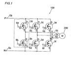
- a power module 100 constitutes a three-phase inverter circuit connected to a motor 200 or the like.
- the power module 100 includes six MOSFETs 3a to 3f.
- the MOSFETs 3a to 3f denote n-type field effect transistors.
- the power module 100 is an example of the "power converter” and the “semiconductor device” in the present invention.
- the MOSFETs 3a, 3c, and 3e constitute the upper arm of the power module 100, and are examples of the "power conversion element” and the "first power conversion element” in the present invention.
- the MOSFETs 3b, 3d, and 3f constitute the lower arm of the power module 100, and are examples of the "power conversion element” and the "second power conversion element” in the present invention.
- the drains (D) of the MOSFETs 3a, 3c, and 3e are connected to a P-side connection terminal 5a.
- the source (S) of the MOSFET 3b is connected to an N-side connection terminal 5b.
- the source (S) of the MOSFET 3d is connected to the N-side connection terminal 5b.
- the source (S) of the MOSFET 3f is connected to the N-side connection terminal 5b.
- the source (S) of the MOSFET 3a and the drain (D) of the MOSFET 3b are connected to a U-phase connection terminal 5c of a power source of the motor 200.
- the source (S) of the MOSFET 3c and the drain (D) of the MOSFET 3d are connected to a V-phase connection terminal 5d of the power source of the motor 200.
- the source (S) of the MOSFET 3e and the drain (D) of the MOSFET 3f are connected to a W-phase connection terminal 5e of the power source of the motor 200.
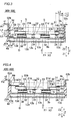
- the structure of the power module 100 is now described with reference to Figs. 2 to 5 .
- the cross-section structure (see Figs. 3 and 4 ) of a portion (portion surrounded by a broken line in Fig. 1 ) of the power module 100 constituting the upper arm and the lower arm of a U-phase is mainly described.
- the cross-section structure of portions of the power module 100 constituting the upper arms and the lower arms of a V-phase and a W-phase is similar to that of the U-phase, and hence the description is omitted.
- a first substrate 1 and a second substrate 2 are arranged in a case portion 4.
- the first substrate 1 located on a lower side and the second substrate 2 located on an upper side are arranged in the case portion 4 while the same are opposed to each other in a direction Z (in a vertical direction).
- the first substrate 1 and the second substrate 2 are based on an insulating material such as ceramic.
- the area of the second substrate 2 located on the upper side is smaller than the area of the first substrate 1 located on the lower side. Specifically, the width W1 in a direction X and the width W2 in a direction Y (see Fig.
- the second substrate 2 located on the upper side can penetrate upward without interfering with the P-side connection terminal 5a (51a) and the N-side connection terminal 5b (51b) (see Fig. 3 ) protruding toward the first substrate 1 from the inner surface of the case portion 4 when the first substrate 1 and the second substrate 2 are inserted into the case portion 4 from below.
- Radiator plates 12a and 12b are formed on the lower surface (in a direction Z1) of the first substrate 1 located on the lower side.
- the radiator plates 12a and 12b are made of copper foil or aluminum foil, for example, and each have a thickness of at least about 100 ⁇ m and not more than about 500 ⁇ m.
- the radiator plate 12a overlaps with a conductive pattern 13a described later provided on the upper surface of the first substrate 1 in plan view (in a direction X-Y), and is substantially opposed to the conductive pattern 13a through the first substrate 1.
- the radiator plate 12b overlaps with a conductive pattern 13b (MOSFET 3b) and a conductive pattern 13c in plan view (in the direction X-Y), and is substantially opposed to the conductive pattern 13b and the conductive pattern 13c through the first substrate 1.
- the radiator plates 12a and 12b are provided symmetrically with the conductive patterns 13a to 13c through the first substrate 1.
- the radiator plate 12a is an example of the "first radiator plate” in the present invention.
- the radiator plate 12b is an example of the "second radiator plate” in the present invention.
- the conductive patterns 13a, 13b, and 13c are provided on the upper surface (in a direction Z2) of the first substrate 1 located on the lower side.
- the conductive patterns 13a to 13c are made of copper foil, for example, and each have a thickness of at least about 100 ⁇ m and not more than about 500 ⁇ m.
- the conductive patterns 13a to 13c each have a thickness equal to those of the radiator plates 12a and 12b, whereby the warpage of the first substrate 1 that may be generated by stress resulting from a heating and cooling cycle can be inhibited.
- the conductive pattern 13a is so formed that a portion 131a thereof (see Fig. 5 ) on an end in a direction X1 is connected to the P-side connection terminal 5a.
- the conductive pattern 13b is so formed that a portion 131b thereof (see Fig. 5 ) on an end in a direction X2 is connected to the U-phase connection terminal 5c (see Fig. 4 ).
- the conductive pattern 13c is so formed that a portion 131c thereof (see Fig. 5 ) on an end in the direction X2 is connected to the N-side connection terminal 5b.
- the portions 131a to 131c connected to the connection terminals are provided on edges of the first substrate 1 located on the lower side.
- the conductive patterns 13a to 13c are examples of the "first conductor pattern" in the present invention.
- the portions 131a to 131c connected to the connection terminals are examples of the "connection portion" in the present invention.
- Conductive patterns 21a and 21d are formed on the lower surface (in the direction Z1) of the second substrate 2 located on the upper side. As shown in Fig. 4 , a conductive pattern 22a (22d) is formed on a portion corresponding to the gate (G) of the MOSFET 3a (3b). Conductive patterns 23a and 23b are formed on the upper surface (in the direction Z2) of the second substrate 2 located on the upper side.
- the conductive patterns 23a and 23b are examples of the "second conductor pattern" in the present invention.
- a gate connection terminal 6a (6b) provided in the case portion 4 is electrically connected to the gate (G) of the MOSFET 3a (3b) through the conductive pattern 23a (23b) and the conductive pattern 22a (22d).
- the conductive patterns 23a and 23b are so formed that portions 231a and 231b (see Fig. 8 ) where the conductive patterns 23a and 23b are connected to the gate connection terminals 6a and 6b are arranged in the vicinity of ends (edges) of the second substrate 2 located on the upper side.
- the portions 231a and 231b connected to the gate connection terminals are examples of the "connection portion" in the present invention.
- the drain (D) of the MOSFET 3a is mounted on a surface of the conductive pattern 13a of the first substrate 1 located on the lower side through a lower melting solder layer 32.
- the lower melting solder layer 32 is made of Sn-37Pb having a melting temperature of 183°C, for example.
- the source (S) of the MOSFET 3a is connected to the conductive pattern 21a of the second substrate 2 located on the upper side through solder balls 33.
- the solder balls 33 are made of Sn-3Ag-0.5Cu having a melting temperature of 217°C, for example.
- the source (S) of the MOSFET 3a and the conductive pattern 21a of the second substrate 2 located on the upper side are connected to each other by the fifteen solder balls 33 (see Fig. 2 ).
- a columnar conductive member 14a is mounted on a surface of the conductive pattern 13b of the first substrate 1 located on the lower side through a higher melting solder layer 34.
- the higher melting solder layer 34 is made of Sn-3Ag-0.5Cu having a melting temperature of 217°C, for example.
- the conductive member 14a is connected to the conductive pattern 21a of the second substrate 2 through a lower melting solder layer 32.
- the drain (D) of the MOSFET 3b is mounted on a surface of the conductive pattern 13b through a lower melting solder layer 32.
- the source (S) of the MOSFET 3b is connected to the conductive pattern 21d of the second substrate 2 located on the upper side through solder balls 33.
- a columnar conductive member 14b is mounted on a surface of the conductive pattern 13c of the first substrate 1 located on the lower side through a higher melting solder layer 34.
- the conductive member 14b is connected to the conductive pattern 21d of the second substrate 2 located on the upper side through a lower melting solder layer 32.
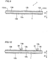
- the case portion 4 is provided to surround the first substrate 1 and the second substrate 2, as shown in Fig. 2 .
- the case portion 4 is formed in the form of a frame in plan view (in the direction X-Y).
- the metallic P-side connection terminal 5a and the metallic N-side connection terminal 5b connected to the conductive patterns 13a and 13c provided on the first substrate 1 are so provided as to be embedded in the case portion 4 made of resin.
- the gate connection terminals 6a and 6b connected to the conductive patterns 23a and 23b provided on the second substrate 2 are so provided as to be embedded in the case portion 4.
- the P-side connection terminal 5a and the N-side connection terminal 5b are formed to supply principal currents (currents for power) to the source (S) of the MOSFET 3a and the drain (D) of the MOSFET 3b.
- the gate connection terminals 6a and 6b are formed to supply control signals (currents for control signals) for turning on/off the MOSFETs to the gates (G) of the MOSFETs 3a and 3b.
- the P-side connection terminal 5a and the N-side connection terminal 5b are examples of the "first connection terminal" in the present invention.
- the gate connection terminals 6a and 6b are examples of the "second connection terminal” in the present invention.
- the first end 51a of the P-side connection terminal 5a is so formed as to protrude toward the first substrate 1 located on the lower side from the inner surface of the case portion 4.
- a second end 52a of the P-side connection terminal 5a is so formed as to bend substantially at 90° and extend in a direction that is away from the side of the first substrate 1 (in the direction X1, toward the outer periphery of the case portion 4) after protruding in the direction Z2 from the upper surface of the case portion 4.
- a portion of the P-side connection terminal 5a other than the first end 51a and the second end 52a is embedded in the case portion 4.
- the first end 51a of the P-side connection terminal 5a is connected to the conductive pattern 13a through a solder layer 31 when the first substrate 1 is arranged in the case portion 4.
- a first end 61a of the gate connection terminal 6a is so formed as to protrude toward the second substrate 2 located on the upper side from the inner surface of the case portion 4.
- a second end 62a of the gate connection terminal 6a is so formed as to bend substantially at 90° and extend in a direction that is away from the side of the second substrate 2 (in the direction X1 toward the outer periphery of the case portion 4) after protruding in the direction Z2 from the upper surface of the case portion 4.
- a portion of the gate connection terminal 6a other than the first end 61a and the second end 62a is embedded in the case portion 4.
- the first end 61a of the gate connection terminal 6a is connected to the conductive pattern 23a through a solder layer 31 when the second substrate 2 is arranged in the case portion 4.
- the power module 100 is so formed that protrusion lengths L2 of portions of the P-side connection terminal 5a and the N-side connection terminal 5b protruding toward the first substrate 1 from the inner surface of the case portion 4 are smaller than a length L1 from the outer peripheral end of the second substrate 2 to the inner surface of the case portion 4, as shown in Fig. 3 (L2 ⁇ L1).
- the P-side connection terminal 5a and the N-side connection terminal 5b can be prevented from intruding into a region where the first substrate 1 and the second substrate 2 are opposed to each other when the MOSFETs are mounted between the first substrate 1 and the second substrate 2.
- the power module 100 is so formed that the protrusion length L2 of the portion of the P-side connection terminal 5a protruding toward the first substrate 1 from the inner surface of the case portion 4 is smaller than protrusion lengths L3 of portions of the gate connection terminals 6a and 6b protruding toward the second substrate 2 from the inner surface of the case portion 4.
- a difference between the vertical position of the first end 51a of the P-side connection terminal 5a (N-side connection terminal 5b) and the vertical position of the first end 61a of the gate connection terminal 6a (gate connection terminal 6b) is L4.
- a difference between the vertical position of a portion (surface of the solder layer 31) of the first substrate 1 connected with the P-side connection terminal 5a (N-side connection terminal 5b) and the vertical position of a portion (surface of the solder layer 31) of the second substrate 2 connected with the gate connection terminal 6a (6b) is L5.
- L4 and L5 are substantially equal to each other.
- the P-side connection terminal 5a and the N-side connection terminal 5b and the gate connection terminals 6a and 6b are deviated not to overlap with each other in plan view (in the direction X-Y).
- the width W5 of the P-side connection terminal 5a (N-side connection terminal 5b) is larger than the width W6 of the gate connection terminal 6a (6b) in plan view (in the direction X-Y) (W5 > W6).
- the thickness t1 of the P-side connection terminal 5a (N-side connection terminal 5b) is substantially equal to the thickness t2 of the gate connection terminal 6a (6b).
- the sectional areas of the P-side connection terminal 5a and the N-side connection terminal 5b in which principal currents flow are larger than the sectional areas of the gate connection terminals 6a and 6b in which control signals flow.
- the sectional area of each connection terminal is set depending on the magnitude of currents flowing in each connection terminal.
- the vertical position of the second end 52a (52b) of the P-side connection terminal 5a (N-side connection terminal 5b) and the vertical position of the second end 62a (62b) of the gate connection terminal 6a (gate connection terminal 6b) are substantially equal to each other.
- the protrusion height H1 (see Fig. 3 ) of the second end 52a (52b) of the P-side connection terminal 5a (N-side connection terminal 5b) from the upper surface of the case portion 4 and the protrusion height H2 (see Fig. 4 ) of the second end 62a (62b) of the gate connection terminal 6a (6b) from the upper surface of the case portion 4 are substantially equal to each other.
- the outer side surface of the first substrate 1 located on the lower side and the upper surfaces of the conductive patterns 13a and 13c come into contact with a lower portion (end surface in the direction Z1)of the case portion 4 when the first substrate 1 and the second substrate 2 are inserted into the case portion 4, whereby a reverse L-shaped positioning portion 4a (see Figs. 3 and 4 ) to position the first substrate 1 located on the lower side is provided on the lower portion of the case portion 4.
- the positioning portion 4a includes a lateral positioning portion 41a to position the outer side surface of the first substrate 1 and a vertical positioning portion 42a coming into contact with the upper surfaces of the conductive patterns 13a and 13c. This positioning portion 4a is circumferentially provided on the lower portion of the frame-shaped case portion 4.
- a sealing member 7 is filled into the case portion 4 to cover the first substrate 1, the second substrate 2, and the MOSFETs 3a and 3b and expose the second end 52a (52b) of the P-side connection terminal 5a (N-side connection terminal 5b) and the second end 62a (62b) of the gate connection terminal 6a (6b).
- the sealing member 7 is made of an insulating member such as liquid epoxy resin.
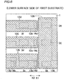
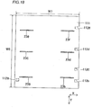
- conductive patterns 13a, 13b, 13c, 13d, and 13e are provided on the upper surface (in the direction Z2) of the first substrate 1 located on the lower side.
- the conductive pattern 13a is electrically connected to the drains (D) of the MOSFETs 3a, 3c, and 3e.
- the conductive pattern 13b is electrically connected to the columnar conductive member 14a and the drain (D) of the MOSFET 3b.
- the conductive pattern 13c is electrically connected to the columnar conductive member 14b (see Fig. 2 ).
- the conductive pattern 13d is electrically connected to a columnar conductive member 14c and the drain (D) of the MOSFET 3d.
- the conductive pattern 13d is so formed that a portion 131d thereof on an end in the direction X2 is connected to the V-phase connection terminal 5d (see Fig. 2 ).
- the conductive pattern 13e is electrically connected to a columnar conductive member 14d and the drain (D) of the MOSFET 3f.
- the conductive pattern 13e is so formed that a portion 131e thereof on an end in the direction X2 is connected to the W-phase connection terminal 5e (see Fig. 2 ).
- the conductive patterns 13d and 13e are examples of the "first conductor pattern" in the present invention.
- the portions 131d and 131e are examples of the "connection portion" in the present invention.
- radiator plates 12a to 12d are formed on the lower surface (in the direction Z1, see Fig. 3 ) of the first substrate 1 located on the lower side.
- the radiator plate 12c is provided to overlap with the conductive pattern 13d (MOSFET 3d) in plan view (in the direction X-Y).
- the radiator plate 12d is provided to overlap with the conductive pattern 13e (MOSFET 3f) in plan view (in the direction X-Y).
- the radiator plates 12c and 12d are examples of the "second radiator plate" in the present invention.
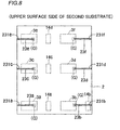
- conductive patterns 21a, 21b, 21c, and 21d are formed on the lower surface (in the direction Z1) of the second substrate 2 located on the upper side.
- the conductive pattern 21a is formed to electrically connect the source (S) of the MOSFET 3a and the conductive member 14a.
- the conductive pattern 22a to electrically connect the gate (G) of the MOSFET 3a and the gate connection terminal 6a (see Fig. 2 ) is provided to be surrounded by the conductive pattern 21a.
- the conductive pattern 21b is formed to electrically connect the source (S) of the MOSFET 3c and the conductive member 14c.
- a conductive pattern 22b to electrically connect the gate (G) of the MOSFET 3c and a gate connection terminal 6c (see Fig. 2 ) is provided to be surrounded by the conductive pattern 21b.
- the conductive pattern 21c is formed to electrically connect the source (S) of the MOSFET 3e and the conductive member 14d.
- a conductive pattern 22c to electrically connect the gate (G) of the MOSFET 3e and a gate connection terminal 6e (see Fig. 2 ) is provided to be surrounded by the conductive pattern 21c.
- the conductive pattern 21d is formed to electrically connect the sources (S) of the MOSFETs 3b, 3d, and 3f and the conductive member 14b.
- a conductive pattern 22d to electrically connect the gate (G) of the MOSFET 3b and the gate connection terminal 6b (see Fig. 2 ) is provided to be surrounded by the conductive pattern 21d.
- a conductive pattern 22e to electrically connect the gate (G) of the MOSFET 3d and a gate connection terminal 6d (see Fig. 2 ) is formed in the vicinity of the conductive pattern 21d.
- a conductive pattern 22f to electrically connect the gate (G) of the MOSFET 3f and a gate connection terminal 6f is formed in the vicinity of the conductive pattern 21d.
- conductive patterns 23a, 23b, 23c, 23d, 23e, and 23f are formed on the upper surface (in the direction Z2) of the second substrate 2 located on the upper side.
- the conductive patterns 23a to 23f are examples of the "second conductor pattern" in the present invention.
- the gate connection terminals 6a to 6f (see Fig. 2 ) provided in the case portion 4 are electrically connected to the gates (G) of the MOSFETs 3a to 3f, respectively, through the conductive patterns 23a to 23f and the conductive patterns 22a to 22f (see Fig. 7 ).
- the conductive patterns 23a to 23f are so formed that portions 231a, 231b, 231c, 231d, 231e, and 231f where the conductive patterns 23a to 23f are connected to the gate connection terminals 6a to 6f are arranged in the vicinity of ends (edges) of the second substrate 2.
- the portions 231a to 231f are examples of the "connection portion" in the present invention.
- the P-side connection terminal 5a, the N-side connection terminal 5b, the U-phase connection terminal 5c, the V-phase connection terminal 5d, and the W-phase connection terminal 5e connected to the conductive patterns 13a to 13e provided on the first substrate 1 are provided to be embedded in the case portion 4. Furthermore, the gate connection terminals 6a to 6f connected to the conductive patterns 23a to 23f provided on the second substrate 2 are provided to be embedded in the case portion 4.
- the P-side connection terminal 5a, the N-side connection terminal 5b, the U-phase connection terminal 5c, the V-phase connection terminal 5d, and the W-phase connection terminal 5e are formed to supply principal currents to the sources (S) or the drains (D) of the MOSFETs 3a to 3f.
- the gate connection terminals 6a to 6f are formed to supply control signals for turning on/off the MOSFETs to the gates (G) of the MOSFETs 3a to 3f.
- the P-side connection terminal 5a, the N-side connection terminal 5b, the U-phase connection terminal 5c, the V-phase connection terminal 5d, and the W-phase connection terminal 5e are examples of the "first connection terminal" in the present invention.
- the gate connection terminals 6a to 6f are examples of the "second connection terminal" in the present invention.
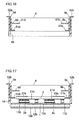
- FIG. 3 and 9 to 17 show a portion of the power module 100 constituting the upper arm and the lower arm of the U-phase, and the arms of the V-phase and the W-phase are also formed simultaneously with that of the U-phase.
- the first substrate 1 having the conductive patterns 13a to 13e made of copper foil formed on the surface in the direction Z2 (upper surface) and the radiator plates 12a to 12d made of copper foil or aluminum foil formed on the surface in the direction Z1 (lower surface) is prepared.
- the conductive members 14a and 14b are mounted on the surfaces of the conductive patterns 13b and 13c, respectively, by the higher melting solder layers 34 made of Sn-3Ag-0.5Cu having a melting temperature of 217°C.
- the conductive members 14c and 14d are mounted on surfaces of the conductive patterns 13d and 13e, respectively, by higher melting solder layers 34.
- the second substrate 2 having the conductive patterns 21a to 21d and the conductive patterns 22a to 22f (see Fig. 7 ) made of copper foil formed on the surface in the direction Z1 (lower surface) and the conductive patterns 23a to 23f made of copper foil formed on the surface in the direction Z2 (upper surface) is prepared.
- the sources (S) of the MOSFETs 3a, 3c, and 3e are mounted to the conductive patterns 21a, 21b, and 21c, respectively, by solder balls 33 made of Sn-3Ag-0.5Cu having a melting temperature of 217°C, for example.
- the gates (G) of the MOSFETs 3a, 3c, and 3e are mounted to the conductive patterns 22a, 22b, and 22c (see Fig. 7 ), respectively, by the solder balls 33.
- the sources (S) of the MOSFETs 3b, 3d, and 3f are mounted to the conductive pattern 21d by solder balls 33.
- the gates (G) of the MOSFETs 3b, 3d, and 3f are mounted to the conductive patterns 22d, 22e, and 22f (see Fig. 7 ), respectively, by the solder balls 33.
- Underfill resin may be filled into clearances between the MOSFETs 3a to 3f and the conductive patterns 21a to 21d when the MOSFETs 3a to 3f are mounted to the conductive patterns 21a to 21d. Consequently, short circuits to the MOSFETs 3a to 3f and the conductive patterns 21a to 21d can be inhibited. Furthermore, the influence (stress) of differences between the thermal expansion coefficients of the MOSFETs 3a to 3f and the thermal expansion coefficient of the second substrate 2 on the solder balls 33 is reduced, and the solder balls 33 and the MOSFETs 3a to 3f (conductive patterns 21a to 21d) that are bonded to each other can be inhibited from separation.
- the MOSFETs 3a to 3f are mounted between the first substrate 1 located on the lower side and the second substrate 2 located on the upper side.
- the drains (D) of the MOSFETs 3a, 3c, and 3e are mounted to the conductive pattern 13a by lower melting solder layers 32 made of Sn-37Pb having a melting temperature of 183°C, for example while the first substrate 1 located on the lower side and the second substrate 2 located on the upper side are opposed to each other.
- the drains (D) of the MOSFETs 3b, 3d, and 3f are mounted to the conductive patterns 13b, 13d, and 13e, respectively, by lower melting solder layers 32.
- the conductive members 14a and 14b (14c, 14d) are mounted to the conductive patterns 21a and 21d (21b, 21c) by the lower melting solder layers 32.
- a reflow process may be performed to mount the MOSFETs 3a to 3f to the conductive patterns 13a to 13e at once after arranging solder sheets in place of the lower melting solder layers 32 and overlapping the second substrate 2 located on the upper side with the first substrate 1 located on the lower side.
- the MOSFETs 3a to 3f can be easily mounted to the conductive patterns 13a to 13e.
- solder having a relatively high melting temperature solder balls 33, higher melting solder layers 34
- solder having a relatively low melting temperature lower melting solder layers 32
- the solder having a relatively low melting temperature can be inhibited from being melted by heat for performing the bonding by solder having a relatively high melting temperature, dissimilarly to a case where the bonding by solder having a relatively high melting temperature is performed after the bonding by solder having a relatively low melting temperature or the reflow process is performed.
- the second substrate 2 is so arranged with respect to the first substrate 1 that the protrusion lengths L2 (see Fig. 2 ) of the portions of the P-side connection terminal 5a and the N-side connection terminal 5b protruding toward the first substrate 1 from the inner surface of the case portion 4 are smaller than the length L1 from the outer peripheral end of the second substrate 2 to the outer peripheral end of the first substrate 1 in plan view (in the direction X-Y) when the first substrate 1 located on the lower side and the second substrate 2 located on the upper side are opposed to each other.
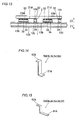
- the case portion 4 made of resin in which the metallic P-side connection terminal 5a, the metallic N-side connection terminal 5b, the metallic U-phase connection terminal 5c, the metallic V-phase connection terminal 5d, and the metallic W-phase connection terminal 5e previously bent automatically by press working or the like shown in Fig. 14 and the metallic gate connection terminals 6a to 6f previously bent automatically by press working or the like shown in Fig. 15 are embedded by insert resin molding, for example is prepared.
- a coating film of a Ni/Au layer may be formed on the surface of each connection terminal by plating before or after the P-side connection terminal 5a, the N-side connection terminal 5b, the U-phase connection terminal 5c, the V-phase connection terminal 5d, the W-phase connection terminal 5e, and the gate connection terminals 6a to 6f are bent.
- the first substrate 1 and the second substrate 2 are inserted into the case portion 4 while the same are opposed to each other.
- the second substrate 2 is smaller than the first substrate 1.
- the protrusion lengths L2 (see Fig. 2 ) of the portions of the P-side connection terminal 5a and the N-side connection terminal 5b protruding toward the first substrate 1 from the inner surface of the case portion 4 are smaller than the length L1 from the outer edge (outer peripheral end) of the second substrate 2 to the outer edge (outer peripheral end) of the first substrate 1.
- the second substrate 2 is inserted into the case portion 4 without interfering with the P-side connection terminal 5a and the N-side connection terminal 5b (U-phase connection terminal 5c, V-phase connection terminal 5d, and W-phase connection terminal 5e).
- the conductive patterns 13a to 13e of the first substrate 1 come into contact with the positioning portion 4a located on the lower portion of the case portion 4 to position the first substrate 1.
- the P-side connection terminal 5a, the N-side connection terminal 5b, the U-phase connection terminal 5c, the V-phase connection terminal 5d, and the W-phase connection terminal 5e are connected to the conductive patterns 13a, 13c, 13b, 13d, and 13e, respectively, by solder layers 31.
- the gate connection terminals 6a to 6f are connected to the conductive patterns 23a to 23f, respectively, by solder layers 31.
- a reflow process may be performed using solder sheets in place of the solder layers 31 to connect the connection terminals to the conductive patterns at once.
- the sealing member 7 is filled into the case portion 4 to cover the first substrate 1, the second substrate 2, and the MOSFETs 3a to 3f and expose the second end 52a of the P-side connection terminal 5a (N-side connection terminal 5b, U-phase connection terminal 5c, V-phase connection terminal 5d, W-phase connection terminal 5e) and the second end 62a of the gate connection terminal 6a (gate connection terminals 6b to 6f).
- the power module 100 is completed.
- the case portion 4 includes the P-side connection terminal 5a (N-side connection terminal 5b, U-phase connection terminal 5c, V-phase connection terminal 5d, W-phase connection terminal 5e) connected to the first substrate 1 and the gate connection terminals 6a to 6f connected to the second substrate 2.
- the p-side connection terminal 5a (N-side connection terminal 5b, U-phase connection terminal 5c, V-phase connection terminal 5d, W-phase connection terminal 5e) and the gate connection terminals 6a to 6f can be electrically connected to the MOSFETs 3a to 3f without using bonding wires extending in a horizontal direction, for example. Consequently, spaces occupied by bonding wires can be reduced, and hence the power module 100 can be miniaturized.
- the sectional area of wiring can be increased while the length of wiring can be decreased as compared with a case of making an electrical connection through a bonding wire extending in the horizontal direction.
- the resistance and the inductance of each connection terminal can be reduced. Consequently, the low-loss power module 100 can be formed.
- the second substrate 2 is formed to be smaller than the first substrate 1 in order to be capable of penetrating without interfering with the P-side connection terminal 5a (N-side connection terminal 5b, U-phase connection terminal 5c, V-phase connection terminal 5d, W-phase connection terminal 5e) protruding toward the first substrate 1 from the inner surface of the case portion 4 when the first substrate 1 and the second substrate 2 are inserted into the case portion 4.
- P-side connection terminal 5a N-side connection terminal 5b, U-phase connection terminal 5c, V-phase connection terminal 5d, W-phase connection terminal 5e
- the P-side connection terminal 5a N-side connection terminal 5b, U-phase connection terminal 5c, V-phase connection terminal 5d, W-phase connection terminal 5e
- the second substrate 2 can be avoided from interfering with each other, and hence the second substrate 2 can be easily arranged in the case portion 4.
- the P-side connection terminal 5a (N-side connection terminal 5b, U-phase connection terminal 5c, V-phase connection terminal 5d, W-phase connection terminal 5e) is prevented from intruding into the region where the first substrate 1 and the second substrate 2 are opposed to each other when the MOSFETs are mounted between the first substrate 1 and the second substrate 2.
- the protrusion length L2 of the portion of the P-side connection terminal 5a (N-side connection terminal 5b, U-phase connection terminal 5c, V-phase connection terminal 5d, W-phase connection terminal 5e) protruding toward the first substrate 1 from the inner surface of the case portion 4 is smaller than the length L1 from the outer peripheral end of the second substrate 2 to the outer peripheral end of the first substrate 1 (inner surface of the case portion 4).
- the P-side connection terminal 5a (N-side connection terminal 5b, U-phase connection terminal 5c, V-phase connection terminal 5d, W-phase connection terminal 5e) and the second substrate 2 can be avoided from interfering with each other.
- the power module 100 is so formed that the protrusion length L2 of the portion of the P-side connection terminal 5a (N-side connection terminal 5b, U-phase connection terminal 5c, V-phase connection terminal 5d, W-phase connection terminal 5e) protruding toward the first substrate 1 from the inner surface of the case portion 4 is smaller than the protrusion lengths L3 of the portions of the gate connection terminals 6a to 6f protruding toward the second substrate 2 from the inner surface of the case portion 4.
- the second substrate 2 can be inserted into the case portion 4 without interfering with the P-side connection terminal 5a (N-side connection terminal 5b, U-phase connection terminal 5c, V-phase connection terminal 5d, W-phase connection terminal 5e). Furthermore, the second substrate 2 and the gate connection terminals 6a to 6f can come into contact with each other when the second substrate 2 is inserted into the case portion 4.
- the power module 100 is so formed that the difference L4 between the vertical position of the first end 51a of the P-side connection terminal 5a (N-side connection terminal 5b, U-phase connection terminal 5c, V-phase connection terminal 5d, W-phase connection terminal 5e) in the case portion 4 and the vertical position of the first end 61a of the gate connection terminal 6a (gate connection terminals 6b to 6f) in the case portion 4 is substantially equal to the difference L5 between the vertical position of the portion of the first substrate 1 connected with the P-side connection terminal 5a (N-side connection terminal 5b, U-phase connection terminal 5c, V-phase connection terminal 5d, W-phase connection terminal 5e) in the case portion 4 and the vertical positions of the portions of the second substrate 2 connected with the gate connection terminals 6a to 6f in the case portion 4.
- the gate connection terminals 6a to 6f and the second substrate 2 also come into contact with each other when the P-side connection terminal 5a (N-side connection terminal 5b, U-phase connection terminal 5c, V-phase connection terminal 5d, W-phase connection terminal 5e) and the first substrate 1 (conductive patterns 13a to 13e) come into contact with each other.
- bonding can be performed at once, and hence bonding by solder can be facilitated to greatly reduce the time required for the bonding.
- the power module 100 is so formed that the vertical position of the second end 52a of the P-side connection terminal 5a (N-side connection terminal 5b, U-phase connection terminal 5c, V-phase connection terminal 5d, W-phase connection terminal 5e) and the vertical position of the second end 62a of the gate connection terminal 6a (gate connection terminals 6b to 6f) are substantially equal to each other.
- the second end 52a of the P-side connection terminal 5a (N-side connection terminal 5b, U-phase connection terminal 5c, V-phase connection terminal 5d, W-phase connection terminal 5e) and the second end 62a of the gate connection terminal 6a (gate connection terminals 6b to 6f) can be easily connected to an external device (substrate connected with a calculation device or an electrically-powered device, for example).
- the gate connection terminals 6a to 6f are electrically connected to the gates (G) of the MOSFETs 3a to 3f through the conductive patterns 23a to 23f of the second substrate 2, respectively.
- no bonding wire extending in the horizontal direction is provided so that the power module 100 can be miniaturized, dissimilarly to a case where the gate connection terminals 6a to 6f are electrically connected to the gates (G) of the MOSFETs 3a to 3f through bonding wires extending in the horizontal direction.
- the outer edge (conductive patterns 13a to 13e) of the first substrate 1 comes into contact with the lower portion (end surface) of the case portion 4 when the first substrate 1 and the second substrate 2 are arranged in the case portion 4, so that the positioning portion 4a to position the first substrate 1 is provided.
- the first substrate 1 can be easily positioned.
- the power module 100 is so formed that the sectional areas of the P-side connection terminal 5a, the N-side connection terminal 5b, the U-phase connection terminal 5c, the V-phase connection terminal 5d, and the W-phase connection terminal 5e are larger than the sectional areas of the gate connection terminals 6a to 6f.
- principal currents to drive the motor that are larger than currents of control signals can flow in the P-side connection terminal 5a, the N-side connection terminal 5b, the U-phase connection terminal 5c, the V-phase connection terminal 5d, and the W-phase connection terminal 5e.
- the sealing member 7 having insulating properties is filled into the case portion 4 to cover the first substrate 1, the second substrate 2, and the MOSFETs 3a to 3f and expose the second end 52a of the P-side connection terminal 5a (N-side connection terminal 5b, U-phase connection terminal 5c, V-phase connection terminal 5d, W-phase connection terminal 5e) and the second end 62a of the gate connection terminal 6a (gate connection terminals 6b to 6f).
- the sealing member 7 having insulating properties is filled into the case portion 4 to cover the first substrate 1, the second substrate 2, and the MOSFETs 3a to 3f and expose the second end 52a of the P-side connection terminal 5a (N-side connection terminal 5b, U-phase connection terminal 5c, V-phase connection terminal 5d, W-phase connection terminal 5e) and the second end 62a of the gate connection terminal 6a (gate connection terminals 6b to 6f).
- the portions 131a to 131e of the P-side connection terminal 5a, the N-side connection terminal 5b, the U-phase connection terminal 5c, the V-phase connection terminal 5d, and the W-phase connection terminal 5e connected to the first substrate 1 and the portions 231a to 231f of the gate connection terminals 6a to 6f connected to the second substrate 2 are provided in the vicinity of the ends (edges) of the first substrate 1 and the second substrate 2.
- the lengths of the P-side connection terminal 5a, the N-side connection terminal 5b, the U-phase connection terminal 5c, the V-phase connection terminal 5d, the W-phase connection terminal 5e, and the gate connection terminals 6a to 6f can be reduced, and hence the resistance and the inductance of each connection terminal can be reduced. Consequently, the low-loss power module 100 can be formed.
- the power module 100 includes the radiator plate 12a provided in a region corresponding to the MOSFETs 3a, 3c, and 3e on the side opposite to the MOSFETs 3a to 3f of the first substrate 1 and the radiator plates 12b, 12c, and 12d provided in regions corresponding to the MOSFETs 3b, 3d, and 3f on the side opposite to the MOSFETs 3a to 3f of the first substrate 1.
- the radiator plates 12b, 12c, and 12d provided in regions corresponding to the MOSFETs 3b, 3d, and 3f on the side opposite to the MOSFETs 3a to 3f of the first substrate 1.
- a power module 110 according to a second embodiment is now described with reference to Figs. 18 and 19 .
- notches 112a to 112e are provided on a second substrate 111, dissimilarly to the first embodiment in which the aforementioned second substrate 2 is smaller than the first substrate 1.
- the power module 110 is an example of the "power converter” and the “semiconductor device" in the present invention.
- the power module 110 is so formed that the width W7 of the second substrate 111 in a direction X and the width W8 of the second substrate 111 in a direction Y are substantially equal to the width W3 of the first substrate 1 (see Fig. 5 ) in the direction X and the width W4 of the first substrate 1 in the direction Y, respectively.
- the notches 112a, 112b, 112c, 112d, and 112e are formed on edges of the second substrate 111.
- the notches 112a to 112e are formed in such a size that the second substrate 111 can pass through the inside of the case portion 4 without interfering with the P-side connection terminal 5a, the N-side connection terminal 5b, the U-phase connection terminal 5c, the V-phase connection terminal 5d, and the W-phase connection terminal 5e when the first substrate 1 and the second substrate 111 are inserted into the case portion 4.
- the remaining structure of the power module 110 according to the second embodiment is similar to that of the power module 100 according to the aforementioned first embodiment.
- the notches 112a to 112e are so formed on the second substrate 111 that the second substrate 111 can penetrate without interfering with the P-side connection terminal 5a, the N-side connection terminal 5b, the U-phase connection terminal 5c, the V-phase connection terminal 5d, and the W-phase connection terminal 5e. Consequently, the second substrate 111 can be inhibited from interfering with the P-side connection terminal 5a, the N-side connection terminal 5b, the U-phase connection terminal 5c, the V-phase connection terminal 5d, and the W-phase connection terminal 5e, and hence the second substrate 111 can be easily arranged in the case portion 4.
- the remaining effects of the second embodiment are similar to those of the aforementioned first embodiment.
- n-type field effect transistor MOSFET
- IGBT IGBT
- diode diode
- the present invention is not restricted to this.
- the P-side connection terminal, the N-side connection terminal, the U-phase connection terminal, the V-phase connection terminal, and the W-phase connection terminal may alternatively be connected to the second substrate while the gate connection terminals may alternatively be connected to the first substrate.
- connection terminals supplying principal currents and the gate connection terminals supplying control signals may alternatively be bent toward the inner periphery of the case portion.
- the portions of the P-side connection terminal, the N-side connection terminal, the U-phase connection terminal, the V-phase connection terminal, the W-phase connection terminal, and the gate connection terminals other than the first ends and the second ends are embedded in the case portion in each of the aforementioned first and second embodiments, the present invention is not restricted to this.
- the portions of the connection terminals other than the first ends and the second ends may alternatively be bonded onto the inner surface of the case portion.
- the positioning portion is provided on the lower surface of the case portion to position the first substrate in each of the aforementioned first and second embodiments, the present invention is not restricted to this.
- a boss-shaped positioning portion protruding from the inner surface of the case portion may alternatively be provided to position the first substrate.
Landscapes
- Engineering & Computer Science (AREA)
- Power Engineering (AREA)
- Microelectronics & Electronic Packaging (AREA)
- Computer Hardware Design (AREA)
- Physics & Mathematics (AREA)
- Condensed Matter Physics & Semiconductors (AREA)
- General Physics & Mathematics (AREA)
- Inverter Devices (AREA)
- Dc-Dc Converters (AREA)
- Power Conversion In General (AREA)
Abstract
Description
- The present invention relates to a power converter and a method for manufacturing a power converter, and more particularly, it relates to a power converter including a connection terminal and a method for manufacturing a power converter.
- A power converter including a connection terminal is known in general.
- Japanese Patent Laying-Open No.
2010-98036 - In the semiconductor device according to the aforementioned Japanese Patent Laying-Open No.
2010-98036 - The present invention has been proposed in order to solve the aforementioned problem, and an object of the present invention is to provide a power converter, a semiconductor device, and a method for manufacturing a power converter each capable of miniaturization.
- In order to attain the aforementioned object, a power converter according to a first aspect of the present invention includes a first substrate, a second substrate arranged to be opposed to the first substrate, a power conversion element mounted between the first substrate and the second substrate, and a case portion provided to surround the first substrate and the second substrate, while the case portion includes a first connection terminal connected to a first conductor pattern arranged on a side of the first substrate closer to the power conversion element and a second connection terminal connected to a second conductor pattern arranged on a side of the second substrate opposite to the power conversion element.
- In the power converter according to the first aspect, the case portion includes the first connection terminal connected to the first conductor pattern arranged on the side of the first substrate closer to the power conversion element and the second connection terminal connected to the second conductor pattern arranged on the side of the second substrate opposite to the power conversion element, whereby the first connection terminal and the second connection terminal can be electrically connected to the power conversion element mounted between the first substrate and the second substrate without using bonding wires extending in a horizontal direction, for example. Thus, the power converter can be miniaturized.
- A method for manufacturing a power converter according to a second aspect of the present invention includes mounting a power conversion element between a first substrate and a second substrate, inserting the first substrate and the second substrate mounted with the power conversion element into a case portion from the second substrate and attaching the first substrate and the second substrate to the case portion, bonding a first connection terminal that the case portion has and a connection portion of a first conductor pattern arranged on the first substrate to each other, and bonding a second connection terminal that the case portion has and a connection portion of a second conductor pattern arranged on the second substrate to each other.
- The method for manufacturing a power converter according to the second aspect includes bonding the first connection terminal that the case portion has and the connection portion of the first conductor pattern arranged on the first substrate to each other and bonding the second connection terminal that the case portion has and the connection portion of the second conductor pattern arranged on the second substrate to each other, whereby the first connection terminal and the second connection terminal can be electrically connected to the power conversion element mounted between the first substrate and the second substrate without using bonding wires extending in a horizontal direction, for example. Thus, the method for manufacturing a power converter capable of miniaturization can be provided.
- The foregoing and other objects, features, aspects and advantages of the present invention will become more apparent from the following detailed description of the present invention when taken in conjunction with the accompanying drawings.
-
-
Fig. 1 is a circuit diagram of a power module according to a first embodiment of the present invention; -
Fig. 2 is a plan view of the power module according to the first embodiment of the present invention; -
Fig. 3 is a sectional view taken along the line 300-300 inFig. 2 ; -
Fig. 4 is a sectional view taken along the line 400-400 inFig. 2 ; -
Fig. 5 is a top plan view of a first substrate of the power module according to the first embodiment of the present invention; -
Fig. 6 is a bottom plan view of the first substrate of the power module according to the first embodiment of the present invention; -
Fig. 7 is a bottom plan view of a second substrate of the power module according to the first embodiment of the present invention; -
Fig. 8 is a top plan view of the second substrate of the power module according to the first embodiment of the present invention; -
Fig. 9 is a diagram for illustrating a step of forming a conductive pattern on the first substrate of the power module according to the first embodiment of the present invention; -
Fig. 10 is a diagram for illustrating a step of mounting a conductive member on the conductive pattern of the first substrate of the power module according to the first embodiment of the present invention; -
Fig. 11 is a diagram for illustrating a step of forming a conductive pattern on the second substrate of the power module according to the first embodiment of the present invention; -
Fig. 12 is a diagram for illustrating a step of mounting a MOSFET on the conductive pattern of the second substrate of the power module according to the first embodiment of the present invention; -
Fig. 13 is a diagram for illustrating a step of stacking the first substrate and the second substrate of the power module according to the first embodiment of the present invention; -
Fig. 14 is a diagram for illustrating a step of forming a P-side (N-side, U-phase, V-phase, W-phase) connection terminal of the power module according to the first embodiment of the present invention; -
Fig. 15 is a diagram for illustrating a step of forming a gate connection terminal of the power module according to the first embodiment of the present invention; -
Fig. 16 is a diagram for illustrating a step of forming a case portion of the power module according to the first embodiment of the present invention; -
Fig. 17 is a diagram for illustrating a step of inserting the first substrate and the second substrate into the case portion of the power module according to the first embodiment of the present invention; -
Fig. 18 is a plan view of a power module according to a second embodiment of the present invention; and -
Fig. 19 is a top plan view of a second substrate of the power module according to the second embodiment of the present invention. - Embodiments of the present invention are now described with reference to the drawings.
- As shown in a circuit diagram in
Fig. 1 , apower module 100 according to a first embodiment of the present invention constitutes a three-phase inverter circuit connected to amotor 200 or the like. Thepower module 100 includes sixMOSFETs 3a to 3f. Here, theMOSFETs 3a to 3f denote n-type field effect transistors. Thepower module 100 is an example of the "power converter" and the "semiconductor device" in the present invention. TheMOSFETs power module 100, and are examples of the "power conversion element" and the "first power conversion element" in the present invention. TheMOSFETs power module 100, and are examples of the "power conversion element" and the "second power conversion element" in the present invention. - The drains (D) of the
MOSFETs side connection terminal 5a. The source (S) of theMOSFET 3b is connected to an N-side connection terminal 5b. The source (S) of theMOSFET 3d is connected to the N-side connection terminal 5b. The source (S) of theMOSFET 3f is connected to the N-side connection terminal 5b. The source (S) of theMOSFET 3a and the drain (D) of theMOSFET 3b are connected to a U-phase connection terminal 5c of a power source of themotor 200. The source (S) of theMOSFET 3c and the drain (D) of theMOSFET 3d are connected to a V-phase connection terminal 5d of the power source of themotor 200. The source (S) of theMOSFET 3e and the drain (D) of theMOSFET 3f are connected to a W-phase connection terminal 5e of the power source of themotor 200. - The structure of the
power module 100 is now described with reference toFigs. 2 to 5 . Here, the cross-section structure (seeFigs. 3 and 4 ) of a portion (portion surrounded by a broken line inFig. 1 ) of thepower module 100 constituting the upper arm and the lower arm of a U-phase is mainly described. The cross-section structure of portions of thepower module 100 constituting the upper arms and the lower arms of a V-phase and a W-phase is similar to that of the U-phase, and hence the description is omitted. - As shown in
Figs. 2 to 4 , afirst substrate 1 and asecond substrate 2 are arranged in acase portion 4. As shown inFigs. 3 and 4 , thefirst substrate 1 located on a lower side and thesecond substrate 2 located on an upper side are arranged in thecase portion 4 while the same are opposed to each other in a direction Z (in a vertical direction). Thefirst substrate 1 and thesecond substrate 2 are based on an insulating material such as ceramic. According to the first embodiment, the area of thesecond substrate 2 located on the upper side is smaller than the area of thefirst substrate 1 located on the lower side. Specifically, the width W1 in a direction X and the width W2 in a direction Y (seeFig. 7 ) of thesecond substrate 2 located on the upper side are smaller than the width W3 in the direction X and the width W4 in the direction Y (seeFig. 5 ) of thefirst substrate 1 located on the lower side, respectively. Thus, thesecond substrate 2 located on the upper side can penetrate upward without interfering with the P-side connection terminal 5a (51a) and the N-side connection terminal 5b (51b) (seeFig. 3 ) protruding toward thefirst substrate 1 from the inner surface of thecase portion 4 when thefirst substrate 1 and thesecond substrate 2 are inserted into thecase portion 4 from below. -
Radiator plates first substrate 1 located on the lower side. Theradiator plates radiator plate 12a overlaps with aconductive pattern 13a described later provided on the upper surface of thefirst substrate 1 in plan view (in a direction X-Y), and is substantially opposed to theconductive pattern 13a through thefirst substrate 1. Theradiator plate 12b overlaps with aconductive pattern 13b (MOSFET 3b) and aconductive pattern 13c in plan view (in the direction X-Y), and is substantially opposed to theconductive pattern 13b and theconductive pattern 13c through thefirst substrate 1. In other words, theradiator plates conductive patterns 13a to 13c through thefirst substrate 1. Thus, the warpage of thefirst substrate 1 that may be generated by stress resulting from a heating and cooling cycle in solder bonding or in operation can be inhibited. Theradiator plate 12a is an example of the "first radiator plate" in the present invention. Theradiator plate 12b is an example of the "second radiator plate" in the present invention. - The
conductive patterns first substrate 1 located on the lower side. Theconductive patterns 13a to 13c are made of copper foil, for example, and each have a thickness of at least about 100 µm and not more than about 500 µm. Theconductive patterns 13a to 13c each have a thickness equal to those of theradiator plates first substrate 1 that may be generated by stress resulting from a heating and cooling cycle can be inhibited. According to the first embodiment, theconductive pattern 13a is so formed that aportion 131a thereof (seeFig. 5 ) on an end in a direction X1 is connected to the P-side connection terminal 5a. Theconductive pattern 13b is so formed that aportion 131b thereof (seeFig. 5 ) on an end in a direction X2 is connected to the U-phase connection terminal 5c (seeFig. 4 ). Theconductive pattern 13c is so formed that a portion 131c thereof (seeFig. 5 ) on an end in the direction X2 is connected to the N-side connection terminal 5b. In other words, theportions 131a to 131c connected to the connection terminals are provided on edges of thefirst substrate 1 located on the lower side. Theconductive patterns 13a to 13c are examples of the "first conductor pattern" in the present invention. Theportions 131a to 131c connected to the connection terminals are examples of the "connection portion" in the present invention. -
Conductive patterns second substrate 2 located on the upper side. As shown inFig. 4 , aconductive pattern 22a (22d) is formed on a portion corresponding to the gate (G) of theMOSFET 3a (3b).Conductive patterns second substrate 2 located on the upper side. Theconductive patterns gate connection terminal 6a (6b) provided in thecase portion 4 is electrically connected to the gate (G) of theMOSFET 3a (3b) through theconductive pattern 23a (23b) and theconductive pattern 22a (22d). Theconductive patterns portions Fig. 8 ) where theconductive patterns gate connection terminals second substrate 2 located on the upper side. Theportions - As shown in
Fig. 3 , the drain (D) of theMOSFET 3a is mounted on a surface of theconductive pattern 13a of thefirst substrate 1 located on the lower side through a lowermelting solder layer 32. The lowermelting solder layer 32 is made of Sn-37Pb having a melting temperature of 183°C, for example. The source (S) of theMOSFET 3a is connected to theconductive pattern 21a of thesecond substrate 2 located on the upper side throughsolder balls 33. Thesolder balls 33 are made of Sn-3Ag-0.5Cu having a melting temperature of 217°C, for example. The source (S) of theMOSFET 3a and theconductive pattern 21a of thesecond substrate 2 located on the upper side are connected to each other by the fifteen solder balls 33 (seeFig. 2 ). - As shown in
Fig. 3 , a columnarconductive member 14a is mounted on a surface of theconductive pattern 13b of thefirst substrate 1 located on the lower side through a highermelting solder layer 34. The highermelting solder layer 34 is made of Sn-3Ag-0.5Cu having a melting temperature of 217°C, for example. Theconductive member 14a is connected to theconductive pattern 21a of thesecond substrate 2 through a lowermelting solder layer 32. The drain (D) of theMOSFET 3b is mounted on a surface of theconductive pattern 13b through a lowermelting solder layer 32. The source (S) of theMOSFET 3b is connected to theconductive pattern 21d of thesecond substrate 2 located on the upper side throughsolder balls 33. - As shown in
Fig. 3 , a columnarconductive member 14b is mounted on a surface of theconductive pattern 13c of thefirst substrate 1 located on the lower side through a highermelting solder layer 34. Theconductive member 14b is connected to theconductive pattern 21d of thesecond substrate 2 located on the upper side through a lowermelting solder layer 32. - The
case portion 4 is provided to surround thefirst substrate 1 and thesecond substrate 2, as shown inFig. 2 . Thecase portion 4 is formed in the form of a frame in plan view (in the direction X-Y). According to the first embodiment, the metallic P-side connection terminal 5a and the metallic N-side connection terminal 5b connected to theconductive patterns first substrate 1 are so provided as to be embedded in thecase portion 4 made of resin. Furthermore, thegate connection terminals conductive patterns second substrate 2 are so provided as to be embedded in thecase portion 4. The P-side connection terminal 5a and the N-side connection terminal 5b are formed to supply principal currents (currents for power) to the source (S) of theMOSFET 3a and the drain (D) of theMOSFET 3b. Thegate connection terminals MOSFETs side connection terminal 5a and the N-side connection terminal 5b are examples of the "first connection terminal" in the present invention. Thegate connection terminals - As shown in
Fig. 3 , thefirst end 51a of the P-side connection terminal 5a is so formed as to protrude toward thefirst substrate 1 located on the lower side from the inner surface of thecase portion 4. Asecond end 52a of the P-side connection terminal 5a is so formed as to bend substantially at 90° and extend in a direction that is away from the side of the first substrate 1 (in the direction X1, toward the outer periphery of the case portion 4) after protruding in the direction Z2 from the upper surface of thecase portion 4. A portion of the P-side connection terminal 5a other than thefirst end 51a and thesecond end 52a is embedded in thecase portion 4. Thefirst end 51a of the P-side connection terminal 5a is connected to theconductive pattern 13a through asolder layer 31 when thefirst substrate 1 is arranged in thecase portion 4. - As shown in
Fig. 4 , afirst end 61a of thegate connection terminal 6a is so formed as to protrude toward thesecond substrate 2 located on the upper side from the inner surface of thecase portion 4. Asecond end 62a of thegate connection terminal 6a is so formed as to bend substantially at 90° and extend in a direction that is away from the side of the second substrate 2 (in the direction X1 toward the outer periphery of the case portion 4) after protruding in the direction Z2 from the upper surface of thecase portion 4. A portion of thegate connection terminal 6a other than thefirst end 61a and thesecond end 62a is embedded in thecase portion 4. Thefirst end 61a of thegate connection terminal 6a is connected to theconductive pattern 23a through asolder layer 31 when thesecond substrate 2 is arranged in thecase portion 4. - According to the first embodiment, the
power module 100 is so formed that protrusion lengths L2 of portions of the P-side connection terminal 5a and the N-side connection terminal 5b protruding toward thefirst substrate 1 from the inner surface of thecase portion 4 are smaller than a length L1 from the outer peripheral end of thesecond substrate 2 to the inner surface of thecase portion 4, as shown inFig. 3 (L2 < L1). Thus, the P-side connection terminal 5a and the N-side connection terminal 5b can be prevented from intruding into a region where thefirst substrate 1 and thesecond substrate 2 are opposed to each other when the MOSFETs are mounted between thefirst substrate 1 and thesecond substrate 2. - According to the first embodiment, the
power module 100 is so formed that the protrusion length L2 of the portion of the P-side connection terminal 5a protruding toward thefirst substrate 1 from the inner surface of thecase portion 4 is smaller than protrusion lengths L3 of portions of thegate connection terminals second substrate 2 from the inner surface of thecase portion 4. A difference between the vertical position of thefirst end 51a of the P-side connection terminal 5a (N-side connection terminal 5b) and the vertical position of thefirst end 61a of thegate connection terminal 6a (gate connection terminal 6b) is L4. A difference between the vertical position of a portion (surface of the solder layer 31) of thefirst substrate 1 connected with the P-side connection terminal 5a (N-side connection terminal 5b) and the vertical position of a portion (surface of the solder layer 31) of thesecond substrate 2 connected with thegate connection terminal 6a (6b) is L5. At this time, L4 and L5 are substantially equal to each other. In other words, when the P-side connection terminal 5a (N-side connection terminal 5b) comes into contact with thesolder layer 31 of thefirst substrate 1, thegate connection terminal 6a (gate connection terminal 6b) also comes into contact with thesolder layer 31 of thesecond substrate 2. - As shown in
Fig. 2 , the P-side connection terminal 5a and the N-side connection terminal 5b and thegate connection terminals side connection terminal 5a (N-side connection terminal 5b) is larger than the width W6 of thegate connection terminal 6a (6b) in plan view (in the direction X-Y) (W5 > W6). As shown inFigs. 3 and 4 , the thickness t1 of the P-side connection terminal 5a (N-side connection terminal 5b) is substantially equal to the thickness t2 of thegate connection terminal 6a (6b). In other words, according to the first embodiment, the sectional areas of the P-side connection terminal 5a and the N-side connection terminal 5b in which principal currents flow are larger than the sectional areas of thegate connection terminals - As shown in
Figs. 3 and 4 , the vertical position of thesecond end 52a (52b) of the P-side connection terminal 5a (N-side connection terminal 5b) and the vertical position of thesecond end 62a (62b) of thegate connection terminal 6a (gate connection terminal 6b) are substantially equal to each other. In other words, the protrusion height H1 (seeFig. 3 ) of thesecond end 52a (52b) of the P-side connection terminal 5a (N-side connection terminal 5b) from the upper surface of thecase portion 4 and the protrusion height H2 (seeFig. 4 ) of thesecond end 62a (62b) of thegate connection terminal 6a (6b) from the upper surface of thecase portion 4 are substantially equal to each other. - According to the first embodiment, the outer side surface of the
first substrate 1 located on the lower side and the upper surfaces of theconductive patterns case portion 4 when thefirst substrate 1 and thesecond substrate 2 are inserted into thecase portion 4, whereby a reverse L-shapedpositioning portion 4a (seeFigs. 3 and 4 ) to position thefirst substrate 1 located on the lower side is provided on the lower portion of thecase portion 4. Specifically, thepositioning portion 4a includes alateral positioning portion 41a to position the outer side surface of thefirst substrate 1 and avertical positioning portion 42a coming into contact with the upper surfaces of theconductive patterns positioning portion 4a is circumferentially provided on the lower portion of the frame-shapedcase portion 4. - According to the first embodiment, a sealing
member 7 is filled into thecase portion 4 to cover thefirst substrate 1, thesecond substrate 2, and theMOSFETs second end 52a (52b) of the P-side connection terminal 5a (N-side connection terminal 5b) and thesecond end 62a (62b) of thegate connection terminal 6a (6b). The sealingmember 7 is made of an insulating member such as liquid epoxy resin. - The planar structure of the U-phase, the V-phase, and the W-phase of the
power module 100 is now described with reference toFigs. 2 and5 to 8 . - As shown in
Fig. 5 ,conductive patterns first substrate 1 located on the lower side. Theconductive pattern 13a is electrically connected to the drains (D) of theMOSFETs conductive pattern 13b is electrically connected to the columnarconductive member 14a and the drain (D) of theMOSFET 3b. Theconductive pattern 13c is electrically connected to the columnarconductive member 14b (seeFig. 2 ). Theconductive pattern 13d is electrically connected to a columnar conductive member 14c and the drain (D) of theMOSFET 3d. Theconductive pattern 13d is so formed that aportion 131d thereof on an end in the direction X2 is connected to the V-phase connection terminal 5d (seeFig. 2 ). Theconductive pattern 13e is electrically connected to a columnarconductive member 14d and the drain (D) of theMOSFET 3f. Theconductive pattern 13e is so formed that aportion 131e thereof on an end in the direction X2 is connected to the W-phase connection terminal 5e (seeFig. 2 ). Theconductive patterns portions - As shown in
Fig. 6 ,radiator plates 12a to 12d are formed on the lower surface (in the direction Z1, seeFig. 3 ) of thefirst substrate 1 located on the lower side. The radiator plate 12c is provided to overlap with theconductive pattern 13d (MOSFET 3d) in plan view (in the direction X-Y). Theradiator plate 12d is provided to overlap with theconductive pattern 13e (MOSFET 3f) in plan view (in the direction X-Y). Theradiator plates 12c and 12d are examples of the "second radiator plate" in the present invention. - As shown in
Fig. 7 ,conductive patterns second substrate 2 located on the upper side. Theconductive pattern 21a is formed to electrically connect the source (S) of theMOSFET 3a and theconductive member 14a. Theconductive pattern 22a to electrically connect the gate (G) of theMOSFET 3a and thegate connection terminal 6a (seeFig. 2 ) is provided to be surrounded by theconductive pattern 21a. Theconductive pattern 21b is formed to electrically connect the source (S) of theMOSFET 3c and the conductive member 14c. Aconductive pattern 22b to electrically connect the gate (G) of theMOSFET 3c and a gate connection terminal 6c (seeFig. 2 ) is provided to be surrounded by theconductive pattern 21b. The conductive pattern 21c is formed to electrically connect the source (S) of theMOSFET 3e and theconductive member 14d. Aconductive pattern 22c to electrically connect the gate (G) of theMOSFET 3e and agate connection terminal 6e (seeFig. 2 ) is provided to be surrounded by the conductive pattern 21c. - The
conductive pattern 21d is formed to electrically connect the sources (S) of theMOSFETs conductive member 14b. Aconductive pattern 22d to electrically connect the gate (G) of theMOSFET 3b and thegate connection terminal 6b (seeFig. 2 ) is provided to be surrounded by theconductive pattern 21d. A conductive pattern 22e to electrically connect the gate (G) of theMOSFET 3d and agate connection terminal 6d (seeFig. 2 ) is formed in the vicinity of theconductive pattern 21d. Aconductive pattern 22f to electrically connect the gate (G) of theMOSFET 3f and agate connection terminal 6f (seeFig. 2 ) is formed in the vicinity of theconductive pattern 21d. - As shown in
Fig. 8 ,conductive patterns second substrate 2 located on the upper side. Theconductive patterns 23a to 23f are examples of the "second conductor pattern" in the present invention. Thegate connection terminals 6a to 6f (seeFig. 2 ) provided in thecase portion 4 are electrically connected to the gates (G) of the MOSFETs 3a to 3f, respectively, through theconductive patterns 23a to 23f and theconductive patterns 22a to 22f (seeFig. 7 ). Theconductive patterns 23a to 23f are so formed thatportions conductive patterns 23a to 23f are connected to thegate connection terminals 6a to 6f are arranged in the vicinity of ends (edges) of thesecond substrate 2. Theportions 231a to 231f are examples of the "connection portion" in the present invention. - As shown in
Fig. 2 , the P-side connection terminal 5a, the N-side connection terminal 5b, the U-phase connection terminal 5c, the V-phase connection terminal 5d, and the W-phase connection terminal 5e connected to theconductive patterns 13a to 13e provided on thefirst substrate 1 are provided to be embedded in thecase portion 4. Furthermore, thegate connection terminals 6a to 6f connected to theconductive patterns 23a to 23f provided on thesecond substrate 2 are provided to be embedded in thecase portion 4. The P-side connection terminal 5a, the N-side connection terminal 5b, the U-phase connection terminal 5c, the V-phase connection terminal 5d, and the W-phase connection terminal 5e are formed to supply principal currents to the sources (S) or the drains (D) of the MOSFETs 3a to 3f. Thegate connection terminals 6a to 6f are formed to supply control signals for turning on/off the MOSFETs to the gates (G) of the MOSFETs 3a to 3f. The P-side connection terminal 5a, the N-side connection terminal 5b, the U-phase connection terminal 5c, the V-phase connection terminal 5d, and the W-phase connection terminal 5e are examples of the "first connection terminal" in the present invention. Thegate connection terminals 6a to 6f are examples of the "second connection terminal" in the present invention. - A method for manufacturing the
power module 100 according to the first embodiment is now described with reference toFigs. 3 and9 to 17 .Figs. 3 and9 to 17 show a portion of thepower module 100 constituting the upper arm and the lower arm of the U-phase, and the arms of the V-phase and the W-phase are also formed simultaneously with that of the U-phase. - As shown in
Fig. 9 , thefirst substrate 1 having theconductive patterns 13a to 13e made of copper foil formed on the surface in the direction Z2 (upper surface) and theradiator plates 12a to 12d made of copper foil or aluminum foil formed on the surface in the direction Z1 (lower surface) is prepared. - As shown in
Fig. 10 , theconductive members conductive patterns conductive members 14c and 14d are mounted on surfaces of theconductive patterns - As shown in
Fig. 11 , thesecond substrate 2 having theconductive patterns 21a to 21d and theconductive patterns 22a to 22f (seeFig. 7 ) made of copper foil formed on the surface in the direction Z1 (lower surface) and theconductive patterns 23a to 23f made of copper foil formed on the surface in the direction Z2 (upper surface) is prepared. - As shown in
Fig. 12 , the sources (S) of theMOSFETs conductive patterns solder balls 33 made of Sn-3Ag-0.5Cu having a melting temperature of 217°C, for example. The gates (G) of theMOSFETs conductive patterns Fig. 7 ), respectively, by thesolder balls 33. The sources (S) of theMOSFETs conductive pattern 21d bysolder balls 33. The gates (G) of theMOSFETs conductive patterns Fig. 7 ), respectively, by thesolder balls 33. - Underfill resin may be filled into clearances between the MOSFETs 3a to 3f and the
conductive patterns 21a to 21d when the MOSFETs 3a to 3f are mounted to theconductive patterns 21a to 21d. Consequently, short circuits to the MOSFETs 3a to 3f and theconductive patterns 21a to 21d can be inhibited. Furthermore, the influence (stress) of differences between the thermal expansion coefficients of the MOSFETs 3a to 3f and the thermal expansion coefficient of thesecond substrate 2 on thesolder balls 33 is reduced, and thesolder balls 33 and the MOSFETs 3a to 3f (conductive patterns 21a to 21d) that are bonded to each other can be inhibited from separation. - As shown in
Fig. 13 , theMOSFETs 3a to 3f are mounted between thefirst substrate 1 located on the lower side and thesecond substrate 2 located on the upper side. Specifically, the drains (D) of theMOSFETs conductive pattern 13a by lower melting solder layers 32 made of Sn-37Pb having a melting temperature of 183°C, for example while thefirst substrate 1 located on the lower side and thesecond substrate 2 located on the upper side are opposed to each other. The drains (D) of theMOSFETs conductive patterns conductive members conductive patterns conductive patterns 13a to 13e at once after arranging solder sheets in place of the lower melting solder layers 32 and overlapping thesecond substrate 2 located on the upper side with thefirst substrate 1 located on the lower side. Thus, theMOSFETs 3a to 3f can be easily mounted to theconductive patterns 13a to 13e. Bonding by solder having a relatively high melting temperature (solder balls 33, higher melting solder layers 34) is performed, and thereafter bonding by solder having a relatively low melting temperature (lower melting solder layers 32) or the reflow process is performed. Thus, the solder having a relatively low melting temperature can be inhibited from being melted by heat for performing the bonding by solder having a relatively high melting temperature, dissimilarly to a case where the bonding by solder having a relatively high melting temperature is performed after the bonding by solder having a relatively low melting temperature or the reflow process is performed. - The
second substrate 2 is so arranged with respect to thefirst substrate 1 that the protrusion lengths L2 (seeFig. 2 ) of the portions of the P-side connection terminal 5a and the N-side connection terminal 5b protruding toward thefirst substrate 1 from the inner surface of thecase portion 4 are smaller than the length L1 from the outer peripheral end of thesecond substrate 2 to the outer peripheral end of thefirst substrate 1 in plan view (in the direction X-Y) when thefirst substrate 1 located on the lower side and thesecond substrate 2 located on the upper side are opposed to each other. - Then, the case portion 4 (see
Fig. 16 ) made of resin in which the metallic P-side connection terminal 5a, the metallic N-side connection terminal 5b, the metallic U-phase connection terminal 5c, the metallic V-phase connection terminal 5d, and the metallic W-phase connection terminal 5e previously bent automatically by press working or the like shown inFig. 14 and the metallicgate connection terminals 6a to 6f previously bent automatically by press working or the like shown inFig. 15 are embedded by insert resin molding, for example is prepared. A coating film of a Ni/Au layer may be formed on the surface of each connection terminal by plating before or after the P-side connection terminal 5a, the N-side connection terminal 5b, the U-phase connection terminal 5c, the V-phase connection terminal 5d, the W-phase connection terminal 5e, and thegate connection terminals 6a to 6f are bent. - As shown in
Fig. 17 , thefirst substrate 1 and thesecond substrate 2 are inserted into thecase portion 4 while the same are opposed to each other. As described above, thesecond substrate 2 is smaller than thefirst substrate 1. Furthermore, the protrusion lengths L2 (seeFig. 2 ) of the portions of the P-side connection terminal 5a and the N-side connection terminal 5b protruding toward thefirst substrate 1 from the inner surface of thecase portion 4 are smaller than the length L1 from the outer edge (outer peripheral end) of thesecond substrate 2 to the outer edge (outer peripheral end) of thefirst substrate 1. Thus, thesecond substrate 2 is inserted into thecase portion 4 without interfering with the P-side connection terminal 5a and the N-side connection terminal 5b (U-phase connection terminal 5c, V-phase connection terminal 5d, and W-phase connection terminal 5e). As shown inFig. 3 , theconductive patterns 13a to 13e of thefirst substrate 1 come into contact with thepositioning portion 4a located on the lower portion of thecase portion 4 to position thefirst substrate 1. Thereafter, the P-side connection terminal 5a, the N-side connection terminal 5b, the U-phase connection terminal 5c, the V-phase connection terminal 5d, and the W-phase connection terminal 5e are connected to theconductive patterns gate connection terminals 6a to 6f are connected to theconductive patterns 23a to 23f, respectively, by solder layers 31. A reflow process may be performed using solder sheets in place of the solder layers 31 to connect the connection terminals to the conductive patterns at once. - Finally, the sealing
member 7 is filled into thecase portion 4 to cover thefirst substrate 1, thesecond substrate 2, and the MOSFETs 3a to 3f and expose thesecond end 52a of the P-side connection terminal 5a (N-side connection terminal 5b, U-phase connection terminal 5c, V-phase connection terminal 5d, W-phase connection terminal 5e) and thesecond end 62a of thegate connection terminal 6a (gate connection terminals 6b to 6f). Thus, thepower module 100 is completed. - According to the first embodiment, as hereinabove described, the
case portion 4 includes the P-side connection terminal 5a (N-side connection terminal 5b, U-phase connection terminal 5c, V-phase connection terminal 5d, W-phase connection terminal 5e) connected to thefirst substrate 1 and thegate connection terminals 6a to 6f connected to thesecond substrate 2. Thus, the p-side connection terminal 5a (N-side connection terminal 5b, U-phase connection terminal 5c, V-phase connection terminal 5d, W-phase connection terminal 5e) and thegate connection terminals 6a to 6f can be electrically connected to the MOSFETs 3a to 3f without using bonding wires extending in a horizontal direction, for example. Consequently, spaces occupied by bonding wires can be reduced, and hence thepower module 100 can be miniaturized. - Furthermore, the sectional area of wiring can be increased while the length of wiring can be decreased as compared with a case of making an electrical connection through a bonding wire extending in the horizontal direction. Thus, the resistance and the inductance of each connection terminal can be reduced. Consequently, the low-
loss power module 100 can be formed. - According to the first embodiment, as hereinabove described, the
second substrate 2 is formed to be smaller than thefirst substrate 1 in order to be capable of penetrating without interfering with the P-side connection terminal 5a (N-side connection terminal 5b, U-phase connection terminal 5c, V-phase connection terminal 5d, W-phase connection terminal 5e) protruding toward thefirst substrate 1 from the inner surface of thecase portion 4 when thefirst substrate 1 and thesecond substrate 2 are inserted into thecase portion 4. Thus, the P-side connection terminal 5a (N-side connection terminal 5b, U-phase connection terminal 5c, V-phase connection terminal 5d, W-phase connection terminal 5e) and thesecond substrate 2 can be avoided from interfering with each other, and hence thesecond substrate 2 can be easily arranged in thecase portion 4. - According to the first embodiment, as hereinabove described, the P-
side connection terminal 5a (N-side connection terminal 5b, U-phase connection terminal 5c, V-phase connection terminal 5d, W-phase connection terminal 5e) is prevented from intruding into the region where thefirst substrate 1 and thesecond substrate 2 are opposed to each other when the MOSFETs are mounted between thefirst substrate 1 and thesecond substrate 2. In other words, the protrusion length L2 of the portion of the P-side connection terminal 5a (N-side connection terminal 5b, U-phase connection terminal 5c, V-phase connection terminal 5d, W-phase connection terminal 5e) protruding toward thefirst substrate 1 from the inner surface of thecase portion 4 is smaller than the length L1 from the outer peripheral end of thesecond substrate 2 to the outer peripheral end of the first substrate 1 (inner surface of the case portion 4). Thus, the P-side connection terminal 5a (N-side connection terminal 5b, U-phase connection terminal 5c, V-phase connection terminal 5d, W-phase connection terminal 5e) and thesecond substrate 2 can be avoided from interfering with each other. - According to the first embodiment, as hereinabove described, the
power module 100 is so formed that the protrusion length L2 of the portion of the P-side connection terminal 5a (N-side connection terminal 5b, U-phase connection terminal 5c, V-phase connection terminal 5d, W-phase connection terminal 5e) protruding toward thefirst substrate 1 from the inner surface of thecase portion 4 is smaller than the protrusion lengths L3 of the portions of thegate connection terminals 6a to 6f protruding toward thesecond substrate 2 from the inner surface of thecase portion 4. Thus, thesecond substrate 2 can be inserted into thecase portion 4 without interfering with the P-side connection terminal 5a (N-side connection terminal 5b, U-phase connection terminal 5c, V-phase connection terminal 5d, W-phase connection terminal 5e). Furthermore, thesecond substrate 2 and thegate connection terminals 6a to 6f can come into contact with each other when thesecond substrate 2 is inserted into thecase portion 4. - According to the first embodiment, as hereinabove described, the
power module 100 is so formed that the difference L4 between the vertical position of thefirst end 51a of the P-side connection terminal 5a (N-side connection terminal 5b, U-phase connection terminal 5c, V-phase connection terminal 5d, W-phase connection terminal 5e) in thecase portion 4 and the vertical position of thefirst end 61a of thegate connection terminal 6a (gate connection terminals 6b to 6f) in thecase portion 4 is substantially equal to the difference L5 between the vertical position of the portion of thefirst substrate 1 connected with the P-side connection terminal 5a (N-side connection terminal 5b, U-phase connection terminal 5c, V-phase connection terminal 5d, W-phase connection terminal 5e) in thecase portion 4 and the vertical positions of the portions of thesecond substrate 2 connected with thegate connection terminals 6a to 6f in thecase portion 4. Thus, thegate connection terminals 6a to 6f and the second substrate 2 (conductive patterns 23a to 23f) also come into contact with each other when the P-side connection terminal 5a (N-side connection terminal 5b, U-phase connection terminal 5c, V-phase connection terminal 5d, W-phase connection terminal 5e) and the first substrate 1 (conductive patterns 13a to 13e) come into contact with each other. In other words, bonding can be performed at once, and hence bonding by solder can be facilitated to greatly reduce the time required for the bonding. - According to the first embodiment, as hereinabove described, the
power module 100 is so formed that the vertical position of thesecond end 52a of the P-side connection terminal 5a (N-side connection terminal 5b, U-phase connection terminal 5c, V-phase connection terminal 5d, W-phase connection terminal 5e) and the vertical position of thesecond end 62a of thegate connection terminal 6a (gate connection terminals 6b to 6f) are substantially equal to each other. Thus, thesecond end 52a of the P-side connection terminal 5a (N-side connection terminal 5b, U-phase connection terminal 5c, V-phase connection terminal 5d, W-phase connection terminal 5e) and thesecond end 62a of thegate connection terminal 6a (gate connection terminals 6b to 6f) can be easily connected to an external device (substrate connected with a calculation device or an electrically-powered device, for example). - According to the first embodiment, as hereinabove described, the
gate connection terminals 6a to 6f are electrically connected to the gates (G) of the MOSFETs 3a to 3f through theconductive patterns 23a to 23f of thesecond substrate 2, respectively. Thus, no bonding wire extending in the horizontal direction is provided so that thepower module 100 can be miniaturized, dissimilarly to a case where thegate connection terminals 6a to 6f are electrically connected to the gates (G) of the MOSFETs 3a to 3f through bonding wires extending in the horizontal direction. - According to the first embodiment, as hereinabove described, the outer edge (
conductive patterns 13a to 13e) of thefirst substrate 1 comes into contact with the lower portion (end surface) of thecase portion 4 when thefirst substrate 1 and thesecond substrate 2 are arranged in thecase portion 4, so that thepositioning portion 4a to position thefirst substrate 1 is provided. Thus, thefirst substrate 1 can be easily positioned. - According to the first embodiment, as hereinabove described, the
power module 100 is so formed that the sectional areas of the P-side connection terminal 5a, the N-side connection terminal 5b, the U-phase connection terminal 5c, the V-phase connection terminal 5d, and the W-phase connection terminal 5e are larger than the sectional areas of thegate connection terminals 6a to 6f. Thus, principal currents to drive the motor that are larger than currents of control signals can flow in the P-side connection terminal 5a, the N-side connection terminal 5b, the U-phase connection terminal 5c, the V-phase connection terminal 5d, and the W-phase connection terminal 5e. - According to the first embodiment, as hereinabove described, the sealing
member 7 having insulating properties is filled into thecase portion 4 to cover thefirst substrate 1, thesecond substrate 2, and the MOSFETs 3a to 3f and expose thesecond end 52a of the P-side connection terminal 5a (N-side connection terminal 5b, U-phase connection terminal 5c, V-phase connection terminal 5d, W-phase connection terminal 5e) and thesecond end 62a of thegate connection terminal 6a (gate connection terminals 6b to 6f). Thus, short circuits between the MOSFETs 3a to 3f and short circuits between the connection terminals can be inhibited so that the reliability of thepower module 100 is improved. - According to the first embodiment, as hereinabove described, the
portions 131a to 131e of the P-side connection terminal 5a, the N-side connection terminal 5b, the U-phase connection terminal 5c, the V-phase connection terminal 5d, and the W-phase connection terminal 5e connected to thefirst substrate 1 and theportions 231a to 231f of thegate connection terminals 6a to 6f connected to thesecond substrate 2 are provided in the vicinity of the ends (edges) of thefirst substrate 1 and thesecond substrate 2. Thus, the lengths of the P-side connection terminal 5a, the N-side connection terminal 5b, the U-phase connection terminal 5c, the V-phase connection terminal 5d, the W-phase connection terminal 5e, and thegate connection terminals 6a to 6f can be reduced, and hence the resistance and the inductance of each connection terminal can be reduced. Consequently, the low-loss power module 100 can be formed. - According to the first embodiment, as hereinabove described, the
power module 100 includes theradiator plate 12a provided in a region corresponding to theMOSFETs first substrate 1 and theradiator plates MOSFETs first substrate 1. Thus, heat generated by theMOSFETs 3a to 3f can be efficiently radiated by theradiator plates 12a to 12d to improve radiation performance. - A
power module 110 according to a second embodiment is now described with reference toFigs. 18 and19 . According to this second embodiment,notches 112a to 112e are provided on asecond substrate 111, dissimilarly to the first embodiment in which the aforementionedsecond substrate 2 is smaller than thefirst substrate 1. Thepower module 110 is an example of the "power converter" and the "semiconductor device" in the present invention. - As shown in
Fig. 19 , thepower module 110 according to the second embodiment is so formed that the width W7 of thesecond substrate 111 in a direction X and the width W8 of thesecond substrate 111 in a direction Y are substantially equal to the width W3 of the first substrate 1 (seeFig. 5 ) in the direction X and the width W4 of thefirst substrate 1 in the direction Y, respectively. As shown inFigs. 18 and19 , thenotches second substrate 111. Thenotches 112a to 112e are formed in such a size that thesecond substrate 111 can pass through the inside of thecase portion 4 without interfering with the P-side connection terminal 5a, the N-side connection terminal 5b, the U-phase connection terminal 5c, the V-phase connection terminal 5d, and the W-phase connection terminal 5e when thefirst substrate 1 and thesecond substrate 111 are inserted into thecase portion 4. The remaining structure of thepower module 110 according to the second embodiment is similar to that of thepower module 100 according to the aforementioned first embodiment. - According to the second embodiment, as hereinabove described, the
notches 112a to 112e are so formed on thesecond substrate 111 that thesecond substrate 111 can penetrate without interfering with the P-side connection terminal 5a, the N-side connection terminal 5b, the U-phase connection terminal 5c, the V-phase connection terminal 5d, and the W-phase connection terminal 5e. Consequently, thesecond substrate 111 can be inhibited from interfering with the P-side connection terminal 5a, the N-side connection terminal 5b, the U-phase connection terminal 5c, the V-phase connection terminal 5d, and the W-phase connection terminal 5e, and hence thesecond substrate 111 can be easily arranged in thecase portion 4. The remaining effects of the second embodiment are similar to those of the aforementioned first embodiment. - Although the present invention has been described and illustrated in detail, it is clearly understood that the same is by way of illustration and example only and is not to be taken by way of limitation, the spirit and scope of the present invention being limited only by the terms of the appended claims.
- For example, while the n-type field effect transistor (MOSFET) is employed as the power conversion element in the present invention in each of the aforementioned first and second embodiments, the present invention is not restricted to this. In the present invention, a p-type field effect transistor, an IGBT, a diode, etc. may alternatively be employed as the power conversion element.
- While the P-side connection terminal, the N-side connection terminal, the U-phase connection terminal, the V-phase connection terminal, and the W-phase connection terminal are connected to the first substrate while the gate connection terminals are connected to the second substrate in each of the aforementioned first and second embodiments, the present invention is not restricted to this. For example, the P-side connection terminal, the N-side connection terminal, the U-phase connection terminal, the V-phase connection terminal, and the W-phase connection terminal may alternatively be connected to the second substrate while the gate connection terminals may alternatively be connected to the first substrate.
- While the P-side connection terminal, the N-side connection terminal, the U-phase connection terminal, the V-phase connection terminal, and the W-phase connection terminal each supplying principal currents and the gate connection terminals each supplying control signals are bent toward the outer periphery of the case portion in each of the aforementioned first and second embodiments, the present invention is not restricted to this. For example, the connection terminals supplying principal currents and the gate connection terminals supplying control signals may alternatively be bent toward the inner periphery of the case portion.
- While the portions of the P-side connection terminal, the N-side connection terminal, the U-phase connection terminal, the V-phase connection terminal, the W-phase connection terminal, and the gate connection terminals other than the first ends and the second ends are embedded in the case portion in each of the aforementioned first and second embodiments, the present invention is not restricted to this. For example, the portions of the connection terminals other than the first ends and the second ends may alternatively be bonded onto the inner surface of the case portion.
- While the positioning portion is provided on the lower surface of the case portion to position the first substrate in each of the aforementioned first and second embodiments, the present invention is not restricted to this. For example, a boss-shaped positioning portion protruding from the inner surface of the case portion may alternatively be provided to position the first substrate.
Claims (15)
- A power converter (100, 110) comprising:a first substrate (1);a second substrate (2, 111) arranged to be opposed to said first substrate;a power conversion element (3a to 3f) mounted between said first substrate and said second substrate; anda case portion (4) provided to surround said first substrate and said second substrate, whereinsaid case portion includes a first connection terminal (5a to 5e) connected to a first conductor pattern (13a to 13c) arranged on a side of said first substrate closer to said power conversion element and a second connection terminal (6a to 6f) connected to a second conductor pattern (23a to 23f) arranged on a side of said second substrate opposite to said power conversion element.
- The power converter according to claim 1, wherein
a first end of said first connection terminal of said case portion is so formed as to protrude toward said first substrate from an inner surface of said case portion, and
said second substrate is formed in such a size or a shape that said second substrate can pass through an inside of said case portion without interfering with said first connection terminal in order to allow said first substrate and said second substrate mounted with said power conversion element to be inserted into said case portion from said second substrate and be attached to said case portion. - The power converter according to claim 2, wherein
said second substrate is formed to be smaller than said first substrate. - The power converter according to claim 3, wherein
a protrusion length of a portion of said first connection terminal protruding toward said first substrate from said inner surface of said case portion is smaller than a length from an outer peripheral end of said second substrate to said inner surface of said case portion not to intrude into a region where said first substrate and said second substrate are opposed to each other. - The power converter according to claim 3 or 4, wherein
a first end of said second connection terminal of said case portion is so formed as to protrude toward said second substrate from said inner surface of said case portion, and
a protrusion length of a portion of said first connection terminal protruding toward said first substrate from said inner surface of said case portion is smaller than a protrusion length of a portion of said second connection terminal protruding toward said second substrate from said inner surface of said case portion. - The power converter according to claim 2, wherein
said second substrate is formed with a notch (112a to 112e) on an edge thereof to be capable of passing through said inside of said case portion without interfering with said first connection terminal. - The power converter according to any one of claims 1 to 6, wherein
a first end of said first connection terminal of said case portion is so formed as to protrude toward said first substrate from an inner surface of said case portion while a first end of said second connection terminal of said case portion is so formed as to protrude toward said second substrate from said inner surface of said case portion, and
a difference between a vertical position of said first end of said first connection terminal of said case portion and a vertical position of said first end of said second connection terminal of said case portion is substantially equal to a difference between a vertical position of a connection portion (131a to 131e) of said first conductor pattern and a vertical position of a connection portion (231a to 231f) of said second conductor pattern so that said first end of said first connection terminal of said case portion comes into contact with said connection portion of said first conductor pattern arranged on said side of said first substrate closer to said power conversion element while said first end of said second connection terminal of said case portion comes into contact with said connection portion of said second conductor pattern arranged on said side of said second substrate opposite to said power conversion element. - The power converter according to any one of claims 1 to 7, wherein
second ends of said first connection terminal and said second connection terminal of said case portion are extracted from a first end surface of said case portion, and are bent toward an outer periphery or an inner periphery of said case portion such that vertical positions of said second ends of said first connection terminal and said second connection terminal are substantially equal to each other. - The power converter according to any one of claims 1 to 8, wherein
said second conductor pattern arranged on said side of said second substrate opposite to said power conversion element is electrically connected to said power conversion element. - The power converter according to any one of claims 1 to 9, wherein
a positioning portion (4a) to position said first substrate when an outer edge of said first substrate comes into contact with said positioning portion is provided on a second end surface of said case portion. - The power converter according to any one of claims 1 to 10, wherein
said first connection terminal supplies at least either principal currents or control signals while said second connection terminal supplies control signals, and
a sectional area of said first connection terminal supplying principal currents is larger than a sectional area of said second connection terminal. - The power converter according to any one of claims 1 to 11, further comprising a sealing member (7) having insulating properties, filled into said case portion to cover said first substrate, said second substrate, and said power conversion element and expose second ends of said first connection terminal and said second connection terminal.
- The power converter according to any one of claims 1 to 12, wherein
a connection portion of said first conductor pattern connected to said first connection terminal and a connection portion of said second conductor pattern connected to said second connection terminal are provided on edges of said first substrate and said second substrate, respectively. - The power converter according to any one of claims 1 to 13, wherein
a radiator plate (12a to 12d) is provided on a surface of said first substrate opposite to a surface on which said power conversion element is set. - A method for manufacturing a power converter, comprising:mounting a power conversion element (3a to 3f) between a first substrate (1) and a second substrate (2, 111) ;inserting said first substrate and said second substrate mounted with said power conversion element into a case portion (4) from said second substrate and attaching said first substrate and said second substrate to said case portion;bonding a first connection terminal (5a to 5e) that said case portion has and a connection portion (131a.to 131e) of a first conductor pattern (13a to 13e) arranged on said first substrate to each other; andbonding a second connection terminal (6a to 6f) that said case portion has and a connection portion (231a to 231f) of a second conductor pattern (23a to 23f) arranged on said second substrate to each other.
Applications Claiming Priority (1)
| Application Number | Priority Date | Filing Date | Title |
|---|---|---|---|
| JP2011121499A JP5387620B2 (en) | 2011-05-31 | 2011-05-31 | Power conversion device, semiconductor device, and method of manufacturing power conversion device |
Publications (2)
| Publication Number | Publication Date |
|---|---|
| EP2530712A2 true EP2530712A2 (en) | 2012-12-05 |
| EP2530712A3 EP2530712A3 (en) | 2015-01-07 |
Family
ID=45656247
Family Applications (1)
| Application Number | Title | Priority Date | Filing Date |
|---|---|---|---|
| EP12156285.4A Withdrawn EP2530712A3 (en) | 2011-05-31 | 2012-02-21 | Power converter and method for manufacturing power converter |
Country Status (4)
| Country | Link |
|---|---|
| US (1) | US8981552B2 (en) |
| EP (1) | EP2530712A3 (en) |
| JP (1) | JP5387620B2 (en) |
| CN (1) | CN102810526B (en) |
Cited By (2)
| Publication number | Priority date | Publication date | Assignee | Title |
|---|---|---|---|---|
| CN105633059A (en) * | 2014-11-25 | 2016-06-01 | 株式会社电装 | Electronic device having heat conducting member |
| EP3944310A1 (en) * | 2020-07-21 | 2022-01-26 | Shinko Electric Industries Co., Ltd. | Semiconductor device |
Families Citing this family (21)
| Publication number | Priority date | Publication date | Assignee | Title |
|---|---|---|---|---|
| JP5460653B2 (en) * | 2011-07-14 | 2014-04-02 | 本田技研工業株式会社 | Semiconductor device |
| JP6120704B2 (en) * | 2013-07-03 | 2017-04-26 | 三菱電機株式会社 | Semiconductor device |
| US9349709B2 (en) | 2013-12-04 | 2016-05-24 | Infineon Technologies Ag | Electronic component with sheet-like redistribution structure |
| JP6390166B2 (en) * | 2014-05-22 | 2018-09-19 | 株式会社デンソー | Power supply |
| KR101755769B1 (en) | 2014-10-29 | 2017-07-07 | 현대자동차주식회사 | Dual side cooling power module and Method for manufacturing the same |
| JP6198068B2 (en) * | 2014-11-19 | 2017-09-20 | 株式会社デンソー | Electronic equipment |
| JP6272213B2 (en) * | 2014-11-26 | 2018-01-31 | 三菱電機株式会社 | Semiconductor device |
| JP6500562B2 (en) * | 2015-03-31 | 2019-04-17 | アイシン・エィ・ダブリュ株式会社 | Semiconductor module |
| DE102016120778B4 (en) * | 2016-10-31 | 2024-01-25 | Infineon Technologies Ag | Assembly with vertically spaced, partially encapsulated contact structures |
| EP3596826B1 (en) * | 2017-03-15 | 2024-05-01 | ABB Schweiz AG | A solid state switching device |
| JP6765336B2 (en) * | 2017-04-06 | 2020-10-07 | 三菱電機株式会社 | Power semiconductor devices, their manufacturing methods, and power conversion devices |
| EP3410481A1 (en) * | 2017-06-01 | 2018-12-05 | HS Elektronik Systeme GmbH | Power semiconductor chip module |
| JP6785729B2 (en) * | 2017-07-12 | 2020-11-18 | 三菱電機株式会社 | Power module |
| CN109923667B (en) * | 2017-10-10 | 2022-11-25 | 新电元工业株式会社 | Semiconductor device and power conversion device |
| JP6919725B2 (en) * | 2018-01-19 | 2021-08-18 | 三菱電機株式会社 | Semiconductor device, its manufacturing method and power conversion device |
| CN108447827B (en) * | 2018-03-17 | 2020-04-17 | 临沂金霖电子有限公司 | Packaging module of power conversion circuit |
| JP2021525958A (en) * | 2018-05-29 | 2021-09-27 | アペックス マイクロテクノロジー インコーポレイテッドApex Microtechnology,Inc. | Thermally conductive electronics packaging |
| JP7135930B2 (en) * | 2019-02-20 | 2022-09-13 | 株式会社デンソー | Semiconductor module and power converter using it |
| EP3761357A1 (en) * | 2019-07-04 | 2021-01-06 | Infineon Technologies Austria AG | Semiconductor device |
| DE102022213628A1 (en) | 2022-12-14 | 2024-06-20 | Robert Bosch Gesellschaft mit beschränkter Haftung | Power module |
| DE102022213629A1 (en) | 2022-12-14 | 2024-06-20 | Robert Bosch Gesellschaft mit beschränkter Haftung | Power module |
Citations (1)
| Publication number | Priority date | Publication date | Assignee | Title |
|---|---|---|---|---|
| JP2010098036A (en) | 2008-10-15 | 2010-04-30 | Fuji Electric Systems Co Ltd | Resin case and method of manufacturing the same |
Family Cites Families (13)
| Publication number | Priority date | Publication date | Assignee | Title |
|---|---|---|---|---|
| JP2765278B2 (en) | 1991-05-31 | 1998-06-11 | 株式会社デンソー | Electronic device manufacturing method |
| JP3410969B2 (en) * | 1997-06-30 | 2003-05-26 | 株式会社東芝 | Semiconductor device |
| US6060772A (en) | 1997-06-30 | 2000-05-09 | Kabushiki Kaisha Toshiba | Power semiconductor module with a plurality of semiconductor chips |
| US6072240A (en) * | 1998-10-16 | 2000-06-06 | Denso Corporation | Semiconductor chip package |
| JP2002026251A (en) * | 2000-07-11 | 2002-01-25 | Toshiba Corp | Semiconductor device |
| US6891256B2 (en) * | 2001-10-22 | 2005-05-10 | Fairchild Semiconductor Corporation | Thin, thermally enhanced flip chip in a leaded molded package |
| DE10231091A1 (en) * | 2002-07-10 | 2004-01-22 | Robert Bosch Gmbh | Active rectifier module for three-phase generators of vehicles |
| JP2004236470A (en) * | 2003-01-31 | 2004-08-19 | Yaskawa Electric Corp | Power module and motor integrated with power module |
| JP4450230B2 (en) * | 2005-12-26 | 2010-04-14 | 株式会社デンソー | Semiconductor device |
| JP2007251076A (en) * | 2006-03-20 | 2007-09-27 | Hitachi Ltd | Power semiconductor module |
| JP5434914B2 (en) | 2008-06-12 | 2014-03-05 | 株式会社安川電機 | Power module and control method thereof |
| DE112009001638B4 (en) * | 2008-07-10 | 2020-07-16 | Mitsubishi Electric Corporation | Power semiconductor module |
| WO2011115081A1 (en) * | 2010-03-16 | 2011-09-22 | 富士電機システムズ株式会社 | Semiconductor device |
-
2011
- 2011-05-31 JP JP2011121499A patent/JP5387620B2/en not_active Expired - Fee Related
-
2012
- 2012-02-20 US US13/400,117 patent/US8981552B2/en not_active Expired - Fee Related
- 2012-02-21 EP EP12156285.4A patent/EP2530712A3/en not_active Withdrawn
- 2012-02-27 CN CN201210046858.2A patent/CN102810526B/en not_active Expired - Fee Related
Patent Citations (1)
| Publication number | Priority date | Publication date | Assignee | Title |
|---|---|---|---|---|
| JP2010098036A (en) | 2008-10-15 | 2010-04-30 | Fuji Electric Systems Co Ltd | Resin case and method of manufacturing the same |
Cited By (4)
| Publication number | Priority date | Publication date | Assignee | Title |
|---|---|---|---|---|
| CN105633059A (en) * | 2014-11-25 | 2016-06-01 | 株式会社电装 | Electronic device having heat conducting member |
| CN105633059B (en) * | 2014-11-25 | 2019-05-14 | 株式会社电装 | Electronic device with heat conduction member |
| EP3944310A1 (en) * | 2020-07-21 | 2022-01-26 | Shinko Electric Industries Co., Ltd. | Semiconductor device |
| US11817381B2 (en) | 2020-07-21 | 2023-11-14 | Shinko Electric Industries Co., Ltd. | Semiconductor device |
Also Published As
| Publication number | Publication date |
|---|---|
| US20120307541A1 (en) | 2012-12-06 |
| JP5387620B2 (en) | 2014-01-15 |
| JP2012249491A (en) | 2012-12-13 |
| EP2530712A3 (en) | 2015-01-07 |
| CN102810526B (en) | 2015-09-23 |
| US8981552B2 (en) | 2015-03-17 |
| CN102810526A (en) | 2012-12-05 |
Similar Documents
| Publication | Publication Date | Title |
|---|---|---|
| EP2530712A2 (en) | Power converter and method for manufacturing power converter | |
| CN101807533B (en) | Semiconductor die package and preparation method thereof | |
| US7618896B2 (en) | Semiconductor die package including multiple dies and a common node structure | |
| TWI430407B (en) | Stacked dual chip package and method of fabrication | |
| US9734944B2 (en) | Electronic package structure comprising a magnetic body and an inductive element and method for making the same | |
| KR20110117211A (en) | Semiconductor die package and method for making the same | |
| US20120083071A1 (en) | Semiconductor die package including low stress configuration | |
| US9159676B2 (en) | Semiconductor module | |
| KR101569769B1 (en) | Semiconductor package with clip structure and fabricating method for the same | |
| JP7512659B2 (en) | Semiconductor module and method for manufacturing the same | |
| JP5613100B2 (en) | Manufacturing method of semiconductor device | |
| JP2020072095A (en) | Power unit, method of manufacturing the same, electric device having power unit, and heat sink | |
| JP2020072094A (en) | Power unit, method of manufacturing the same, and electric device having power unit | |
| US20240071898A1 (en) | Semiconductor device and semiconductor device manufacturing method | |
| JP2020072101A (en) | Power unit, method of manufacturing the same, electric device having power unit, and heat sink |
Legal Events
| Date | Code | Title | Description |
|---|---|---|---|
| PUAI | Public reference made under article 153(3) epc to a published international application that has entered the european phase |
Free format text: ORIGINAL CODE: 0009012 |
|
| AK | Designated contracting states |
Kind code of ref document: A2 Designated state(s): AL AT BE BG CH CY CZ DE DK EE ES FI FR GB GR HR HU IE IS IT LI LT LU LV MC MK MT NL NO PL PT RO RS SE SI SK SM TR |
|
| AX | Request for extension of the european patent |
Extension state: BA ME |
|
| RIC1 | Information provided on ipc code assigned before grant |
Ipc: H01L 23/498 20060101ALI20140818BHEP Ipc: H02M 7/00 20060101ALI20140818BHEP Ipc: H01L 23/049 20060101ALI20140818BHEP Ipc: H01L 25/07 20060101AFI20140818BHEP Ipc: H01L 21/60 20060101ALI20140818BHEP |
|
| PUAL | Search report despatched |
Free format text: ORIGINAL CODE: 0009013 |
|
| AK | Designated contracting states |
Kind code of ref document: A3 Designated state(s): AL AT BE BG CH CY CZ DE DK EE ES FI FR GB GR HR HU IE IS IT LI LT LU LV MC MK MT NL NO PL PT RO RS SE SI SK SM TR |
|
| AX | Request for extension of the european patent |
Extension state: BA ME |
|
| RIC1 | Information provided on ipc code assigned before grant |
Ipc: H01L 23/498 20060101ALI20141202BHEP Ipc: H01L 23/049 20060101ALI20141202BHEP Ipc: H01L 21/60 20060101ALI20141202BHEP Ipc: H02M 7/00 20060101ALI20141202BHEP Ipc: H01L 25/07 20060101AFI20141202BHEP |
|
| 17P | Request for examination filed |
Effective date: 20150417 |
|
| RBV | Designated contracting states (corrected) |
Designated state(s): AL AT BE BG CH CY CZ DE DK EE ES FI FR GB GR HR HU IE IS IT LI LT LU LV MC MK MT NL NO PL PT RO RS SE SI SK SM TR |
|
| STAA | Information on the status of an ep patent application or granted ep patent |
Free format text: STATUS: THE APPLICATION HAS BEEN WITHDRAWN |
|
| 18W | Application withdrawn |
Effective date: 20160707 |