EP2528066A1 - Electron-beam-curable electrically conductive paste and process for production of circuit board using same - Google Patents
Electron-beam-curable electrically conductive paste and process for production of circuit board using same Download PDFInfo
- Publication number
- EP2528066A1 EP2528066A1 EP11734709A EP11734709A EP2528066A1 EP 2528066 A1 EP2528066 A1 EP 2528066A1 EP 11734709 A EP11734709 A EP 11734709A EP 11734709 A EP11734709 A EP 11734709A EP 2528066 A1 EP2528066 A1 EP 2528066A1
- Authority
- EP
- European Patent Office
- Prior art keywords
- electroconductive
- electron beam
- circuit board
- mass
- radical polymerizable
- Prior art date
- Legal status (The legal status is an assumption and is not a legal conclusion. Google has not performed a legal analysis and makes no representation as to the accuracy of the status listed.)
- Withdrawn
Links
Images
Classifications
-
- C—CHEMISTRY; METALLURGY
- C08—ORGANIC MACROMOLECULAR COMPOUNDS; THEIR PREPARATION OR CHEMICAL WORKING-UP; COMPOSITIONS BASED THEREON
- C08F—MACROMOLECULAR COMPOUNDS OBTAINED BY REACTIONS ONLY INVOLVING CARBON-TO-CARBON UNSATURATED BONDS
- C08F2/00—Processes of polymerisation
- C08F2/46—Polymerisation initiated by wave energy or particle radiation
- C08F2/54—Polymerisation initiated by wave energy or particle radiation by X-rays or electrons
-
- C—CHEMISTRY; METALLURGY
- C08—ORGANIC MACROMOLECULAR COMPOUNDS; THEIR PREPARATION OR CHEMICAL WORKING-UP; COMPOSITIONS BASED THEREON
- C08J—WORKING-UP; GENERAL PROCESSES OF COMPOUNDING; AFTER-TREATMENT NOT COVERED BY SUBCLASSES C08B, C08C, C08F, C08G or C08H
- C08J7/00—Chemical treatment or coating of shaped articles made of macromolecular substances
- C08J7/04—Coating
- C08J7/0427—Coating with only one layer of a composition containing a polymer binder
-
- C—CHEMISTRY; METALLURGY
- C08—ORGANIC MACROMOLECULAR COMPOUNDS; THEIR PREPARATION OR CHEMICAL WORKING-UP; COMPOSITIONS BASED THEREON
- C08J—WORKING-UP; GENERAL PROCESSES OF COMPOUNDING; AFTER-TREATMENT NOT COVERED BY SUBCLASSES C08B, C08C, C08F, C08G or C08H
- C08J7/00—Chemical treatment or coating of shaped articles made of macromolecular substances
- C08J7/04—Coating
- C08J7/043—Improving the adhesiveness of the coatings per se, e.g. forming primers
-
- C—CHEMISTRY; METALLURGY
- C08—ORGANIC MACROMOLECULAR COMPOUNDS; THEIR PREPARATION OR CHEMICAL WORKING-UP; COMPOSITIONS BASED THEREON
- C08J—WORKING-UP; GENERAL PROCESSES OF COMPOUNDING; AFTER-TREATMENT NOT COVERED BY SUBCLASSES C08B, C08C, C08F, C08G or C08H
- C08J7/00—Chemical treatment or coating of shaped articles made of macromolecular substances
- C08J7/04—Coating
- C08J7/044—Forming conductive coatings; Forming coatings having anti-static properties
-
- C—CHEMISTRY; METALLURGY
- C08—ORGANIC MACROMOLECULAR COMPOUNDS; THEIR PREPARATION OR CHEMICAL WORKING-UP; COMPOSITIONS BASED THEREON
- C08J—WORKING-UP; GENERAL PROCESSES OF COMPOUNDING; AFTER-TREATMENT NOT COVERED BY SUBCLASSES C08B, C08C, C08F, C08G or C08H
- C08J7/00—Chemical treatment or coating of shaped articles made of macromolecular substances
- C08J7/04—Coating
- C08J7/046—Forming abrasion-resistant coatings; Forming surface-hardening coatings
-
- C—CHEMISTRY; METALLURGY
- C08—ORGANIC MACROMOLECULAR COMPOUNDS; THEIR PREPARATION OR CHEMICAL WORKING-UP; COMPOSITIONS BASED THEREON
- C08J—WORKING-UP; GENERAL PROCESSES OF COMPOUNDING; AFTER-TREATMENT NOT COVERED BY SUBCLASSES C08B, C08C, C08F, C08G or C08H
- C08J7/00—Chemical treatment or coating of shaped articles made of macromolecular substances
- C08J7/12—Chemical modification
- C08J7/16—Chemical modification with polymerisable compounds
- C08J7/18—Chemical modification with polymerisable compounds using wave energy or particle radiation
-
- C—CHEMISTRY; METALLURGY
- C09—DYES; PAINTS; POLISHES; NATURAL RESINS; ADHESIVES; COMPOSITIONS NOT OTHERWISE PROVIDED FOR; APPLICATIONS OF MATERIALS NOT OTHERWISE PROVIDED FOR
- C09D—COATING COMPOSITIONS, e.g. PAINTS, VARNISHES OR LACQUERS; FILLING PASTES; CHEMICAL PAINT OR INK REMOVERS; INKS; CORRECTING FLUIDS; WOODSTAINS; PASTES OR SOLIDS FOR COLOURING OR PRINTING; USE OF MATERIALS THEREFOR
- C09D5/00—Coating compositions, e.g. paints, varnishes or lacquers, characterised by their physical nature or the effects produced; Filling pastes
- C09D5/24—Electrically-conducting paints
-
- C—CHEMISTRY; METALLURGY
- C09—DYES; PAINTS; POLISHES; NATURAL RESINS; ADHESIVES; COMPOSITIONS NOT OTHERWISE PROVIDED FOR; APPLICATIONS OF MATERIALS NOT OTHERWISE PROVIDED FOR
- C09D—COATING COMPOSITIONS, e.g. PAINTS, VARNISHES OR LACQUERS; FILLING PASTES; CHEMICAL PAINT OR INK REMOVERS; INKS; CORRECTING FLUIDS; WOODSTAINS; PASTES OR SOLIDS FOR COLOURING OR PRINTING; USE OF MATERIALS THEREFOR
- C09D7/00—Features of coating compositions, not provided for in group C09D5/00; Processes for incorporating ingredients in coating compositions
- C09D7/40—Additives
- C09D7/60—Additives non-macromolecular
- C09D7/63—Additives non-macromolecular organic
-
- H—ELECTRICITY
- H01—ELECTRIC ELEMENTS
- H01B—CABLES; CONDUCTORS; INSULATORS; SELECTION OF MATERIALS FOR THEIR CONDUCTIVE, INSULATING OR DIELECTRIC PROPERTIES
- H01B1/00—Conductors or conductive bodies characterised by the conductive materials; Selection of materials as conductors
- H01B1/20—Conductive material dispersed in non-conductive organic material
- H01B1/22—Conductive material dispersed in non-conductive organic material the conductive material comprising metals or alloys
-
- H—ELECTRICITY
- H05—ELECTRIC TECHNIQUES NOT OTHERWISE PROVIDED FOR
- H05K—PRINTED CIRCUITS; CASINGS OR CONSTRUCTIONAL DETAILS OF ELECTRIC APPARATUS; MANUFACTURE OF ASSEMBLAGES OF ELECTRICAL COMPONENTS
- H05K1/00—Printed circuits
- H05K1/02—Details
- H05K1/09—Use of materials for the conductive, e.g. metallic pattern
- H05K1/092—Dispersed materials, e.g. conductive pastes or inks
- H05K1/095—Dispersed materials, e.g. conductive pastes or inks for polymer thick films, i.e. having a permanent organic polymeric binder
-
- C—CHEMISTRY; METALLURGY
- C08—ORGANIC MACROMOLECULAR COMPOUNDS; THEIR PREPARATION OR CHEMICAL WORKING-UP; COMPOSITIONS BASED THEREON
- C08J—WORKING-UP; GENERAL PROCESSES OF COMPOUNDING; AFTER-TREATMENT NOT COVERED BY SUBCLASSES C08B, C08C, C08F, C08G or C08H
- C08J2433/00—Characterised by the use of homopolymers or copolymers of compounds having one or more unsaturated aliphatic radicals, each having only one carbon-to-carbon double bond, and only one being terminated by only one carboxyl radical, or of salts, anhydrides, esters, amides, imides, or nitriles thereof; Derivatives of such polymers
- C08J2433/04—Characterised by the use of homopolymers or copolymers of compounds having one or more unsaturated aliphatic radicals, each having only one carbon-to-carbon double bond, and only one being terminated by only one carboxyl radical, or of salts, anhydrides, esters, amides, imides, or nitriles thereof; Derivatives of such polymers esters
- C08J2433/06—Characterised by the use of homopolymers or copolymers of compounds having one or more unsaturated aliphatic radicals, each having only one carbon-to-carbon double bond, and only one being terminated by only one carboxyl radical, or of salts, anhydrides, esters, amides, imides, or nitriles thereof; Derivatives of such polymers esters of esters containing only carbon, hydrogen, and oxygen, the oxygen atom being present only as part of the carboxyl radical
- C08J2433/10—Homopolymers or copolymers of methacrylic acid esters
- C08J2433/12—Homopolymers or copolymers of methyl methacrylate
-
- C—CHEMISTRY; METALLURGY
- C08—ORGANIC MACROMOLECULAR COMPOUNDS; THEIR PREPARATION OR CHEMICAL WORKING-UP; COMPOSITIONS BASED THEREON
- C08K—Use of inorganic or non-macromolecular organic substances as compounding ingredients
- C08K5/00—Use of organic ingredients
- C08K5/0008—Organic ingredients according to more than one of the "one dot" groups of C08K5/01 - C08K5/59
- C08K5/0016—Plasticisers
-
- H—ELECTRICITY
- H05—ELECTRIC TECHNIQUES NOT OTHERWISE PROVIDED FOR
- H05K—PRINTED CIRCUITS; CASINGS OR CONSTRUCTIONAL DETAILS OF ELECTRIC APPARATUS; MANUFACTURE OF ASSEMBLAGES OF ELECTRICAL COMPONENTS
- H05K2203/00—Indexing scheme relating to apparatus or processes for manufacturing printed circuits covered by H05K3/00
- H05K2203/09—Treatments involving charged particles
- H05K2203/092—Particle beam, e.g. using an electron beam or an ion beam
-
- H—ELECTRICITY
- H05—ELECTRIC TECHNIQUES NOT OTHERWISE PROVIDED FOR
- H05K—PRINTED CIRCUITS; CASINGS OR CONSTRUCTIONAL DETAILS OF ELECTRIC APPARATUS; MANUFACTURE OF ASSEMBLAGES OF ELECTRICAL COMPONENTS
- H05K3/00—Apparatus or processes for manufacturing printed circuits
- H05K3/10—Apparatus or processes for manufacturing printed circuits in which conductive material is applied to the insulating support in such a manner as to form the desired conductive pattern
- H05K3/12—Apparatus or processes for manufacturing printed circuits in which conductive material is applied to the insulating support in such a manner as to form the desired conductive pattern using thick film techniques, e.g. printing techniques to apply the conductive material or similar techniques for applying conductive paste or ink patterns
- H05K3/1283—After-treatment of the printed patterns, e.g. sintering or curing methods
Definitions
- the present invention relates to an electroconductive paste for electron beam curing and a circuit board production method that uses the same.
- Circuit boards are used in the membrane switches used in personal computer keyboards, seating sensors, pressure sensors and the like. Some of the circuit boards are composed of a plastic film and an electroconductive layer obtained by printing an electroconductive paste for electron beam curing on the plastic film and curing the paste by irradiating with an electron beam.
- An electroconductive paste that uses a radical polymerizable resin such as an acrylate compound is known as an electroconductive paste for electron beam curing used to form these circuit boards (Patent Documents 1 and 2). Radical polymerizable resins cause an increase in the crosslink density of the electroconductive paste and increase curing shrinkage ratio.
- an electroconductive layer is formed by coating an electroconductive paste for electron beam curing containing a radical polymerizable resin onto a plastic film and curing by irradiating with an electron beam, sufficient hardness can be imparted to the electroconductive layer.
- an electroconductive paste obtained by mixing a cationically polymerizable resin into a radical polymerizable resin is known as an electroconductive paste for electron beam curing (Patent Document 3). Since this electroconductive paste for electron beam curing allows the proportion of radical polymerizable resin to be reduced, curing shrinkage during the curing process can be inhibited.
- the inventors of the present invention found that the electroconductive pastes for electron beam curing described in the above-mentioned Patent Documents 1 to 3 have the problems indicated below. Namely, in the case of producing a circuit board by forming electroconductive layer on a plastic base using the electroconductive pastes for electron beam curing described in Patent Documents 1 to 3 and using the circuit board in a high-temperature environment, adhesion of the electroconductive layer to the plastic film and bendability of the electroconductive layer are insufficient. Consequently, in the case of using the circuit board in a high-temperature environment, the electroconductive layer occasionally separated from the plastic film. Alternatively if the circuit board is repeatedly bent in a high-temperature environment, cracks and the like formed in the electroconductive layer.
- an object of the present invention is to provide an electroconductive paste for electron beam curing capable of forming a circuit board having an electroconductive layer that has superior hardness and bendability as well as superior adhesion to a plastic base even if used in a high-temperature environment, and a circuit board production method that uses this paste.
- Plasticizers have been commonly thought to decrease the hardness of an electroconductive layer as a result of causing a relative decrease in the proportion of high-strength crosslinked resin due to the addition thereof to an electroconductive paste.
- plasticizers either escape from the electroconductive layer or cause a reaction with other components in a high-temperature environment. As a result, they have been commonly thought to subsequently cause a considerable decrease in bendability of the electroconductive layer and adhesion of the electroconductive layer to the plastic base. Consequently, plasticizers have heretofore not been used in the field of electroconductive pastes for electron beam curing.
- the inventors of the present invention formed an electroconductive layer by radiating an electron beam onto an electroconductive paste for electron beam curing obtained by incorporating a plasticizer in a radical polymerizable resin composition at a prescribed ratio. As a result, the inventors of the present invention unexpectedly found that the above-mentioned problems can be solved, thereby leading to completion of the present invention.
- the present invention is an electroconductive paste for electron beam curing having: an electroconductive powder; a radical polymerizable composition; and a plasticizer, wherein the plasticizer is incorporated at a ratio of 5 parts by mass to 20 parts by mass based on 100 parts by mass of the radical polymerizable composition.
- an electroconductive layer when a circuit board is formed by applying the electroconductive paste for electron beam curing onto a plastic base and curing by irradiating with an electron beam to form an electroconductive layer, an electroconductive layer can be obtained that has superior hardness and bendability as well as superior adhesion to the plastic base even if the circuit board is used in a high-temperature environment.
- the inventors of the present invention first heat-cured the above-mentioned electroconductive paste for electron beam curing containing a small amount of a polymerization initiator, and held the resulting electroconductive layer in a high-temperature environment.
- bendability of the electroconductive layer was determined to have decreased slightly and adhesion to the plastic base was determined to have decreased considerably.
- the inventors of the present invention presume that, as a result of the plasticizer volatilizing and escaping during heat curing, the effect of the plasticizer was not sufficiently obtained, and since an adequate crosslink density was not obtained during heat curing, the plasticizer escaped or underwent a chemical reaction with other components as a result of holding the electroconductive paste in a high-temperature environment.
- the plasticizer is preferably a dicarboxylate. In this case, more superior bendability can be imparted to the electroconductive layer. In addition, if the plasticizer is a dicarboxylate, heat resistance, dispersibility and meltability can be further improved.
- the dicarboxylate is preferably dioctyl adipate. In this case, heat resistance can be further improved.
- the plasticizer is preferably incorporated at a ratio of 5 parts by mass to 10 parts by mass based on 100 parts by mass of the radical polymerizable composition. In this case, more superior hardness tends to be able to be obtained.
- the radical polymerizable composition preferably contains a mixture of a bifunctional urethane-based oligomer and a monofunctional acrylate monomer.
- various coated films can be obtained according to the structure of polyol and the type of isocyanate in the urethane-based oligomer.
- the radical polymerizable composition preferably further contains a di (meth) acrylate having an oxyalkylene unit from the viewpoint of improving heat resistance and improving softening point.
- the present invention is a method for producing a circuit board provided with a plastic base and an electroconductive layer provided on the plastic base, the method including: a step of coating the previously described electroconductive paste for electron beam curing on the plastic base; and a step of obtaining the circuit board by curing the electroconductive paste for electron beam curing by irradiating with an electron beam to form the electroconductive layer.
- a circuit board can be produced having an electroconductive layer that has superior hardness and bendability as well as superior adhesion to the plastic base even if used in a high-temperature environment. Consequently, separation of the electroconductive layer from the plastic base is sufficiently inhibited even if the circuit board is used in a high-temperature environment. In addition, the formation of cracks and the like in the electroconductive layer is sufficienlty inhibited even if the circuit board is repeatedly bent in a high-temperature environment.
- an electroconductive paste for electron beam curing which is capable of forming a circuit board having an electroconductive layer that has superior hardness and bendability as well as superior adhesion to a plastic base even if used in a high-temperature environment, and a circuit board production method that uses that paste, are provided.
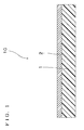
- FIG. 1 is a cross-sectional view showing an example of a circuit board produced according to the circuit board production method according to the present invention.
- a circuit board 10 is provided with a plastic base 1 and an electroconductive layer 2 provided on the plastic base 1.
- the electroconductive layer 2 can be obtained by coating an electroconductive paste for electron beam curing (to be simply referred to as an "electroconductive paste") on the plastic base 1, and curing the electroconductive paste by irradiating with an electron beam.
- an electroconductive paste a paste which contains an electroconductive powder, a radical polymerizable composition and a plasticizer, and in which the plasticizer is incorporated at the ratio of 5 parts by mass to 20 parts by mass based on 100 parts by mass of the radical polymerizable composition is used.
- the electroconductive layer 2 has superior hardness and bendability as well as superior adhesion to the plastic base 1 even if the circuit board 10 is used in a high-temperature environment. Consequently, separation of the electroconductive layer 2 from the plastic base 1 is sufficiently inhibited even if the circuit board 10 is used in a high-temperature environment. In addition, the formation of cracks and the like in the electroconductive layer 2 is sufficiently inhibited even if the circuit board 10 is used while repeatedly bending in a high-temperature environment.
- the electroconductive paste is coated onto the plastic base 1.
- plastic that composes the plastic base 1 provided it is a plastic.
- plastics include polyester resins such as polyethylene terephthalate resin (PET) or polyethylene naphthalate resin (PEN).
- the electroconductive paste contains an electroconductive powder, a radical polymerizable composition and a plasticizer as previously described.
- electroconductive powders examples include not only metals such as gold, silver, copper, platinum, palladium, nickel or alloys of two or more types thereof, but also carriers such as plastics, ceramics, or the like coated with the above-mentioned metals.
- Silver is preferably used for the above-mentioned metal since it demonstrates only a small decrease in electrical conductivity caused by oxidation.
- the shape of the electroconductive powder there are no particular limitations on the shape of the electroconductive powder, and examples of the shape of the electroconductive powder include scales, needles and spheres.
- the mean particle diameter of the electroconductive powder is normally 0.5 ⁇ m to 15 ⁇ m and preferably 1 ⁇ m to 5 ⁇ m.
- radical polymerizable composition Radical polymerizable material
- the radical polymerizable composition is a material that undergoes radical polymerization when irradiated with an electron beam
- the radical polymerizable composition contains, for example, polyester (meth)acrylate, polyurethane (meth)acrylate or polyether (meth) acrylate. These may be used alone or two or more types may be used as a mixture.
- polyurethane (meth) acrylate is preferable since it allows the obtaining of various coated films according to the structure of polyol and the type of isocyanate.
- polyurethane (meth)acrylate can be obtained by, for example, reacting a bifunctional urethane-based oligomer with a monofunctional acrylate monomer
- the radical polymerizable composition may contain a mixture of polyurethane (meth)acrylate in the form of a bifunctional urethane-based oligomer and a monofunctional acrylate monomer which are the raw materials of polyurethane (meth)acrylate.
- the radical polymerizable composition may further contain a di(meth)acrylate having an oxyalkylene unit.
- di (meth) acrylates having an oxyalkylene unit examples include polyethylene glycol di(meth)acrylate and polypropylene glycol di(meth)acrylate, polyethylene glycol diacrylate is preferable in terms of further improving the reaction rate.
- Polyethylene glycol diacrylate has repeating units having a polyethylene glycol structure (-CH 2 CH 2 O-). Although there are no particular limitations on the number n of these repeating units, it is preferably an integer of 5 to 10.
- the content of the radical polymerizable composition in the electroconductive paste is normally 5% by mass to 30% by mass and preferably 10% by mass to 20% by mass.
- plasticizers examples include dicarboxylates, phosphates, polyesters and epoxidized vegetable oils and the like. These can be used alone or two or more types can be used as a mixture. Among these, dicarboxylates are used preferably since they improve heat resistance, dispersibility and meltability.
- Dicarboxylates are obtained by esterification of a dicarboxylic acid and an alcohol.
- dicarboxylic acids examples include fatty acids such as oxalic acid, malonic acid, succinic acid, glutaric acid, adipic acid, pimelic acid, suberic acid, azelaic acid or sebacic acid, and aromatic acids such as phthalic acid, isophthalic acid or terephthalic acid.
- alcohols examples include alkyl alcohols such as capryl alcohol, lauryl alcohol, myristyl alcohol, cetyl alcohol, stearyl alcohol, oleyl alcohol or linoyl alcohol.
- the dicarboxylate is particularly preferably dioctyl adipate obtained by reacting adipic acid and capryl alcohol. In this case, heat resistance can be further improved.
- Triphenyl phosphate for example, can be used for the phosphate.
- the plasticizer is incorporated at a ratio of 5 parts by mass to 20 parts by mass based on 100 parts by mass of the radical polymerizable composition. If the ratio at which the plasticizer is incorporated based on 100 parts by mass of the radical polymerizable composition is less than 5 parts by mass, although hardness and adhesion of the electroconductive layer 2 to the plastic base 1 are superior when the circuit board 10 is used in a high-temperature environment, bendability decreases significantly.
- the ratio at which the plasticizer is incorporated based on 100 parts by mass of the radical polymerizable composition exceeds 20 parts by mass, although the electroconductive layer 2 has superior bendability in the case of using the circuit board 10 in a high-temperature environment, hardness and adhesion of the electroconductive layer 2 to the plastic base 1 decrease significantly.
- the plasticizer is preferably incorporated at a ratio of 5 parts by mass to 10 parts by mass based on 100 parts by mass of the radical polymerizable composition. In this case, more superior hardness tends to be able to be obtained.
- the plasticizer preferably has a boiling point of 300°C to 500°C, and more preferably has a boiling point of 300°C to 400°C. Furthermore, if the boiling point of the plasticizer is within the above-mentioned ranges, it becomes difficult for the plasticizer to escape from the electroconductive paste in comparison with the boiling point being lower than 300°C in the case of irradiating the electroconductive paste with an electron beam.
- the electroconductive paste may further contain additives, including a filler such as silica or a flame retardant such as magnesium hydroxide or aluminum hydroxide.
- a filler such as silica
- a flame retardant such as magnesium hydroxide or aluminum hydroxide.
- the total content of the electroconductive powder, radical polymerizable composition, plasticizer and additives is preferably 70% by mass to 100% by mass.
- additives refer to additives other than a polymerization initiator.
- the electroconductive layer 2 is formed by irradiating the electroconductive paste coated on the plastic base 1 with an electron beam.
- the circuit board 10 is obtained in this manner.
- conditions for irradiating with an electron beam normally consist of an absorbed dose of 100 kGy to 300 kGy, and an accelerating voltage of 150 kV to 300 kV.
- plasticizer incorporated based on 100 parts by mass of radical polymerizable composition (parts by mass) 5 10 15 20 10 10 0 3 21.8 Hardness Pencil hardness F B B B B B F B 2B Bendability Initial resistivity ( ⁇ cm) 5.8 ⁇ 10 -5 5.8 ⁇ 10 -5 5.4 ⁇ 10 -5 6.3 ⁇ 10 -5 5.8 ⁇ 10 -5 5.9 ⁇ 10 -5 8.9 ⁇ 10 -5 5.2 ⁇ 10 -5 7.0 ⁇ 10 -5 Resistivity increase rate (%) 94 67 92 54 65 67 149 217 43 Adhesion of electroconductive layer to plastic base (points) 8 8 8 8 8 8 10 8 4
- the electroconductive pastes obtained in Examples 1 to 6 and Comparative Examples 1 to 3 were coated onto a PET film having a thickness of 75 ⁇ m to have a coated thickness of 20 ⁇ m followed by irradiating with an electron beam under conditions of an accelerating voltage of 250 kV and absorbed dose of 200 kGy to form an electroconductive layer and obtain a circuit board.
- the hardness of the electroconductive layers of each of the above mentioned circuit boards was evaluated according to pencil hardness measured in conformity with JIS K-5600-5-5. At this time, circuit boards having an electroconductive layer having a pencil hardness of B or higher were evaluated as acceptable, while circuit boards having an electroconductive layer having a pencil hardness lower than B were evaluated as unacceptable.
- Table 1 a pencil hardness of B or higher refers to a pencil hardness of B or pencil hardness that is harder than B (such as F).
- a pencil hardness of less than B refers to a pencil hardness that is softer than B (such as 2B).
- each circuit board was evaluated based on an increase in resistivity following a bending test carried out after holding each above-mentioned circuit board in an oven set to 80°C for 500 hours.
- resistivity of the electroconductive layer was measured according to the four-probe method using a digital multimeter.
- each circuit board was bent 10 times to a radius of curvature R of 0, followed by measuring resistivity at that time (post-bending resistivity) in the same manner as described above.
- each of the circuit boards to a PET film was evaluated in the manner as indicated below. Namely, adhesion of each of the circuit boards was evaluated in compliance with the crosscut tape test defined in section 8.5.3 of JIS K-5400-8.5. More specifically, first, eleven parallel cuts were made at intervals of 1 mm on the electroconductive layer using a cutter knife. Next, eleven cuts were further made at intervals of 1 mm perpendicular to the first cuts. A large number of fragments were formed in the surface of the electroconductive layer in this manner. Cellophane adhesive tape was then affixed to the electroconductive layer, and the surface of the cellophane adhesive tape was rubbed with an eraser to completely adhere the cellophane adhesive tape to the electroconductive layer.
- one end of the cellophane adhesive tape was instantaneously peeled off while pulling at a right angle to the electroconductive layer.
- adhesion was scored as indicated below corresponding to the proportion of the surface area of the fragments that were peeled off relative to the total surface area of the fragments on the electroconductive layer prior to peeling.
- circuit boards having a score of 8 points or higher were evaluated as having superior adhesion of the electroconductive layer to PET and being acceptable, while circuit boards having a score of less than 8 points were evaluated as having inferior adhesion of the electroconductive layer to PET and being unacceptable.
- electroconductive layers formed by using the electroconductive pastes of Examples 1 to 6 achieved an acceptable level with respect to each of hardness, bendability and adhesion to a PET film.
- electroconductive layers formed by using the electroconductive pastes of Comparative Examples 1 to 3 did not achieve an acceptable level with respect to any of hardness, bendability or adhesion to a PET film.
- the electroconductive paste of the present invention was confirmed to be able to form a circuit board having an electroconductive layer that has superior hardness and bendability as well as superior adhesion to a plastic base even if used in a high-temperature environment.
Landscapes
- Chemical & Material Sciences (AREA)
- Organic Chemistry (AREA)
- Health & Medical Sciences (AREA)
- Chemical Kinetics & Catalysis (AREA)
- Medicinal Chemistry (AREA)
- Polymers & Plastics (AREA)
- Engineering & Computer Science (AREA)
- Dispersion Chemistry (AREA)
- Life Sciences & Earth Sciences (AREA)
- Materials Engineering (AREA)
- Wood Science & Technology (AREA)
- Physics & Mathematics (AREA)
- Spectroscopy & Molecular Physics (AREA)
- Toxicology (AREA)
- General Chemical & Material Sciences (AREA)
- Microelectronics & Electronic Packaging (AREA)
- Conductive Materials (AREA)
- Manufacturing Of Printed Wiring (AREA)
- Coating Of Shaped Articles Made Of Macromolecular Substances (AREA)
- Polymerisation Methods In General (AREA)
- Paints Or Removers (AREA)
Abstract
Description
- The present invention relates to an electroconductive paste for electron beam curing and a circuit board production method that uses the same.
- Circuit boards are used in the membrane switches used in personal computer keyboards, seating sensors, pressure sensors and the like. Some of the circuit boards are composed of a plastic film and an electroconductive layer obtained by printing an electroconductive paste for electron beam curing on the plastic film and curing the paste by irradiating with an electron beam.
- An electroconductive paste that uses a radical polymerizable resin such as an acrylate compound is known as an electroconductive paste for electron beam curing used to form these circuit boards (Patent Documents 1 and 2). Radical polymerizable resins cause an increase in the crosslink density of the electroconductive paste and increase curing shrinkage ratio. In addition, when an electroconductive layer is formed by coating an electroconductive paste for electron beam curing containing a radical polymerizable resin onto a plastic film and curing by irradiating with an electron beam, sufficient hardness can be imparted to the electroconductive layer.
- On the other hand, an electroconductive paste obtained by mixing a cationically polymerizable resin into a radical polymerizable resin is known as an electroconductive paste for electron beam curing (Patent Document 3). Since this electroconductive paste for electron beam curing allows the proportion of radical polymerizable resin to be reduced, curing shrinkage during the curing process can be inhibited.
-
- Patent Document 1: Japanese Patent Publication No.
2758432 - Patent Document 2: Japanese Patent Application Publication No.
H6-157945 - Patent Document 3: Japanese Patent Application Publication No.
2005-15627 - However, the inventors of the present invention found that the electroconductive pastes for electron beam curing described in the above-mentioned Patent Documents 1 to 3 have the problems indicated below. Namely, in the case of producing a circuit board by forming electroconductive layer on a plastic base using the electroconductive pastes for electron beam curing described in Patent Documents 1 to 3 and using the circuit board in a high-temperature environment, adhesion of the electroconductive layer to the plastic film and bendability of the electroconductive layer are insufficient. Consequently, in the case of using the circuit board in a high-temperature environment, the electroconductive layer occasionally separated from the plastic film. Alternatively if the circuit board is repeatedly bent in a high-temperature environment, cracks and the like formed in the electroconductive layer.
- Consequently, there was a need for an electroconductive paste for electron beam curing capable of forming a circuit board having an electroconductive layer that has superior hardness and bendability as well as superior adhesion to a plastic base even if used in a high-temperature environment.
- With the foregoing in view, an object of the present invention is to provide an electroconductive paste for electron beam curing capable of forming a circuit board having an electroconductive layer that has superior hardness and bendability as well as superior adhesion to a plastic base even if used in a high-temperature environment, and a circuit board production method that uses this paste.
- The inventors of the present invention conducted extensive studies focusing on plasticizers in order to solve the above-mentioned problems. Plasticizers have been commonly thought to decrease the hardness of an electroconductive layer as a result of causing a relative decrease in the proportion of high-strength crosslinked resin due to the addition thereof to an electroconductive paste. In addition, plasticizers either escape from the electroconductive layer or cause a reaction with other components in a high-temperature environment. As a result, they have been commonly thought to subsequently cause a considerable decrease in bendability of the electroconductive layer and adhesion of the electroconductive layer to the plastic base. Consequently, plasticizers have heretofore not been used in the field of electroconductive pastes for electron beam curing. However, the inventors of the present invention formed an electroconductive layer by radiating an electron beam onto an electroconductive paste for electron beam curing obtained by incorporating a plasticizer in a radical polymerizable resin composition at a prescribed ratio. As a result, the inventors of the present invention unexpectedly found that the above-mentioned problems can be solved, thereby leading to completion of the present invention.
- Namely, the present invention is an electroconductive paste for electron beam curing having: an electroconductive powder; a radical polymerizable composition; and a plasticizer, wherein the plasticizer is incorporated at a ratio of 5 parts by mass to 20 parts by mass based on 100 parts by mass of the radical polymerizable composition.
- According to this electroconductive paste for electron beam curing, when a circuit board is formed by applying the electroconductive paste for electron beam curing onto a plastic base and curing by irradiating with an electron beam to form an electroconductive layer, an electroconductive layer can be obtained that has superior hardness and bendability as well as superior adhesion to the plastic base even if the circuit board is used in a high-temperature environment.
- Here, although the reason why the above-mentioned effects are obtained are not certain, the inventors of the present invention presume this to be as described below based on the relationship with the result in the case of heat-curing the above-mentioned electroconductive paste.
- Namely, the inventors of the present invention first heat-cured the above-mentioned electroconductive paste for electron beam curing containing a small amount of a polymerization initiator, and held the resulting electroconductive layer in a high-temperature environment. As a result, bendability of the electroconductive layer was determined to have decreased slightly and adhesion to the plastic base was determined to have decreased considerably. With respect to the reason for this, the inventors of the present invention presume that, as a result of the plasticizer volatilizing and escaping during heat curing, the effect of the plasticizer was not sufficiently obtained, and since an adequate crosslink density was not obtained during heat curing, the plasticizer escaped or underwent a chemical reaction with other components as a result of holding the electroconductive paste in a high-temperature environment. In contrast, in the case of irradiating the above-mentioned electroconductive paste for electron beam curing with an electron beam, since heat is not applied during curing, it is presumed to be difficult for the plasticizer to escape. In addition, sufficient crosslink density is obtained as a result of irradiating with an electron beam. Consequently, it is presumed that it is difficult for the plasticizer to escape and to undergo a chemical reaction with other components even if the electroconductive paste is held in a high-temperature environment. Moreover, the plasticizer is incorporated at a low ratio with respect to the radical polymerizable composition, and does not cause a large decrease in the relative ratio of the cured radical polymerizable composition. Consequently, the inventors of the present invention presume that an electroconductive layer could be obtained that has superior hardness and bendability as well as superior adhesion to the plastic base even if the circuit board is used in a high-temperature environment.
- In the above-mentioned electroconductive paste for electron beam curing, the plasticizer is preferably a dicarboxylate. In this case, more superior bendability can be imparted to the electroconductive layer. In addition, if the plasticizer is a dicarboxylate, heat resistance, dispersibility and meltability can be further improved.
- In the above-mentioned electroconductive paste for electron beam curing, the dicarboxylate is preferably dioctyl adipate. In this case, heat resistance can be further improved.
- In the above-mentioned electroconductive paste for electron beam curing, the plasticizer is preferably incorporated at a ratio of 5 parts by mass to 10 parts by mass based on 100 parts by mass of the radical polymerizable composition. In this case, more superior hardness tends to be able to be obtained.
- In the above-mentioned electroconductive paste for electron beam curing, the radical polymerizable composition preferably contains a mixture of a bifunctional urethane-based oligomer and a monofunctional acrylate monomer.
- In this case, various coated films can be obtained according to the structure of polyol and the type of isocyanate in the urethane-based oligomer.
- In the above-mentioned electroconductive paste for electron beam curing, the radical polymerizable composition preferably further contains a di (meth) acrylate having an oxyalkylene unit from the viewpoint of improving heat resistance and improving softening point.
- In addition, the present invention is a method for producing a circuit board provided with a plastic base and an electroconductive layer provided on the plastic base, the method including: a step of coating the previously described electroconductive paste for electron beam curing on the plastic base; and a step of obtaining the circuit board by curing the electroconductive paste for electron beam curing by irradiating with an electron beam to form the electroconductive layer.
- According to this circuit board production method, a circuit board can be produced having an electroconductive layer that has superior hardness and bendability as well as superior adhesion to the plastic base even if used in a high-temperature environment. Consequently, separation of the electroconductive layer from the plastic base is sufficiently inhibited even if the circuit board is used in a high-temperature environment. In addition, the formation of cracks and the like in the electroconductive layer is sufficienlty inhibited even if the circuit board is repeatedly bent in a high-temperature environment.
- According to the present invention, an electroconductive paste for electron beam curing, which is capable of forming a circuit board having an electroconductive layer that has superior hardness and bendability as well as superior adhesion to a plastic base even if used in a high-temperature environment, and a circuit board production method that uses that paste, are provided.
-
-
FIG. 1 is a cross-sectional view showing an example of a circuit board produced according to the circuit board production method according to the present invention. - The following provides a detailed explanation of embodiments of the present invention.
-
FIG. 1 is a cross-sectional view showing an example of a circuit board produced according to the circuit board production method according to the present invention. As shown inFIG. 1 , acircuit board 10 is provided with a plastic base 1 and anelectroconductive layer 2 provided on the plastic base 1. - Here, the
electroconductive layer 2 can be obtained by coating an electroconductive paste for electron beam curing (to be simply referred to as an "electroconductive paste") on the plastic base 1, and curing the electroconductive paste by irradiating with an electron beam. As the electroconductive paste, a paste which contains an electroconductive powder, a radical polymerizable composition and a plasticizer, and in which the plasticizer is incorporated at the ratio of 5 parts by mass to 20 parts by mass based on 100 parts by mass of the radical polymerizable composition is used. - In this
circuit board 10, theelectroconductive layer 2 has superior hardness and bendability as well as superior adhesion to the plastic base 1 even if thecircuit board 10 is used in a high-temperature environment. Consequently, separation of theelectroconductive layer 2 from the plastic base 1 is sufficiently inhibited even if thecircuit board 10 is used in a high-temperature environment. In addition, the formation of cracks and the like in theelectroconductive layer 2 is sufficiently inhibited even if thecircuit board 10 is used while repeatedly bending in a high-temperature environment. - Next, an explanation is provided of a production method of the
circuit board 10. First, the electroconductive paste is coated onto the plastic base 1. - There are no particular limitations on the plastic that composes the plastic base 1 provided it is a plastic. Examples of such plastics include polyester resins such as polyethylene terephthalate resin (PET) or polyethylene naphthalate resin (PEN).
- The electroconductive paste contains an electroconductive powder, a radical polymerizable composition and a plasticizer as previously described.
- Examples of electroconductive powders that can be used include not only metals such as gold, silver, copper, platinum, palladium, nickel or alloys of two or more types thereof, but also carriers such as plastics, ceramics, or the like coated with the above-mentioned metals. Silver is preferably used for the above-mentioned metal since it demonstrates only a small decrease in electrical conductivity caused by oxidation.
- There are no particular limitations on the shape of the electroconductive powder, and examples of the shape of the electroconductive powder include scales, needles and spheres.
- Although there are no particular limitations on the mean particle diameter of the electroconductive powder, it is normally 0.5 µm to 15 µm and preferably 1 µm to 5 µm.
- There are no particular limitations on the radical polymerizable composition (radical polymerizable material) provided it is a material that undergoes radical polymerization when irradiated with an electron beam, and the radical polymerizable composition contains, for example, polyester (meth)acrylate, polyurethane (meth)acrylate or polyether (meth) acrylate. These may be used alone or two or more types may be used as a mixture. Among these, polyurethane (meth) acrylate is preferable since it allows the obtaining of various coated films according to the structure of polyol and the type of isocyanate.
- Furthermore, although polyurethane (meth)acrylate can be obtained by, for example, reacting a bifunctional urethane-based oligomer with a monofunctional acrylate monomer, instead of polyurethane (meth)acrylate, the radical polymerizable composition may contain a mixture of polyurethane (meth)acrylate in the form of a bifunctional urethane-based oligomer and a monofunctional acrylate monomer which are the raw materials of polyurethane (meth)acrylate.
- From the viewpoint of improving heat resistance and improving softening point, the radical polymerizable composition may further contain a di(meth)acrylate having an oxyalkylene unit.
- Although examples of di (meth) acrylates having an oxyalkylene unit include polyethylene glycol di(meth)acrylate and polypropylene glycol di(meth)acrylate, polyethylene glycol diacrylate is preferable in terms of further improving the reaction rate. Polyethylene glycol diacrylate has repeating units having a polyethylene glycol structure (-CH2CH2O-). Although there are no particular limitations on the number n of these repeating units, it is preferably an integer of 5 to 10.
- Although there are no particular limitations on the content of the radical polymerizable composition in the electroconductive paste, it is normally 5% by mass to 30% by mass and preferably 10% by mass to 20% by mass.
- Examples of plasticizers that can be used include dicarboxylates, phosphates, polyesters and epoxidized vegetable oils and the like. These can be used alone or two or more types can be used as a mixture. Among these, dicarboxylates are used preferably since they improve heat resistance, dispersibility and meltability.
- Dicarboxylates are obtained by esterification of a dicarboxylic acid and an alcohol.
- Examples of dicarboxylic acids that can be used include fatty acids such as oxalic acid, malonic acid, succinic acid, glutaric acid, adipic acid, pimelic acid, suberic acid, azelaic acid or sebacic acid, and aromatic acids such as phthalic acid, isophthalic acid or terephthalic acid.
- Examples of alcohols include alkyl alcohols such as capryl alcohol, lauryl alcohol, myristyl alcohol, cetyl alcohol, stearyl alcohol, oleyl alcohol or linoyl alcohol.
- The dicarboxylate is particularly preferably dioctyl adipate obtained by reacting adipic acid and capryl alcohol. In this case, heat resistance can be further improved.
- Triphenyl phosphate, for example, can be used for the phosphate.
- The plasticizer is incorporated at a ratio of 5 parts by mass to 20 parts by mass based on 100 parts by mass of the radical polymerizable composition. If the ratio at which the plasticizer is incorporated based on 100 parts by mass of the radical polymerizable composition is less than 5 parts by mass, although hardness and adhesion of the
electroconductive layer 2 to the plastic base 1 are superior when thecircuit board 10 is used in a high-temperature environment, bendability decreases significantly. Conversely, if the ratio at which the plasticizer is incorporated based on 100 parts by mass of the radical polymerizable composition exceeds 20 parts by mass, although theelectroconductive layer 2 has superior bendability in the case of using thecircuit board 10 in a high-temperature environment, hardness and adhesion of theelectroconductive layer 2 to the plastic base 1 decrease significantly. - The plasticizer is preferably incorporated at a ratio of 5 parts by mass to 10 parts by mass based on 100 parts by mass of the radical polymerizable composition. In this case, more superior hardness tends to be able to be obtained.
- Moreover, from the viewpoint of imparting more superior bendability to the
electroconductive layer 2, the plasticizer preferably has a boiling point of 300°C to 500°C, and more preferably has a boiling point of 300°C to 400°C. Furthermore, if the boiling point of the plasticizer is within the above-mentioned ranges, it becomes difficult for the plasticizer to escape from the electroconductive paste in comparison with the boiling point being lower than 300°C in the case of irradiating the electroconductive paste with an electron beam. - Furthermore, the electroconductive paste may further contain additives, including a filler such as silica or a flame retardant such as magnesium hydroxide or aluminum hydroxide. In the above-mentioned electroconductive paste, the total content of the electroconductive powder, radical polymerizable composition, plasticizer and additives is preferably 70% by mass to 100% by mass. Here, additives refer to additives other than a polymerization initiator.
- Next, the
electroconductive layer 2 is formed by irradiating the electroconductive paste coated on the plastic base 1 with an electron beam. Thecircuit board 10 is obtained in this manner. - Although varying according to the composition of the electroconductive paste and the properties of the
electroconductive layer 2 to be produced, conditions for irradiating with an electron beam normally consist of an absorbed dose of 100 kGy to 300 kGy, and an accelerating voltage of 150 kV to 300 kV. - Although the following provides a more detailed explanation of the contents of the present invention by listing examples and comparative examples thereof, the present invention is not limited to the following examples.
- Silver powder, radical polymerizable composition and plasticizer were mixed at the ratios shown in Table 1 and the mixtures were kneaded with a triple roll mill to obtain electroconductive pastes. Furthermore, a radical polymerizable composition containing a mixture of a bifunctional urethane-based oligomer, a monofunctional acrylate monomer and polyethylene glycol diacrylate (number n of repeating units having a polyethylene glycol structure = 9) was used for the radical polymerizable composition. A polycarbonate-based urethane oligomer was used for the bifunctional urethane-based oligomer. In addition, values in Table 1 for which units are not specifically indicated are represented in units of mass%.
[Table 1] Ex.1 Ex.2 Ex.3 Ex.4 Ex.5 Ex.6 Comp. Ex. 1 Comp. Ex. 2 Comp. Ex. 3 Electroconductive powder Silver powder 85.6 85.0 84.5 83.9 85.0 85.0 86.2 85.8 83.6 Radical polymerizable composition Urethane-based oligomer (bifunctional) 4.57 4.55 4.50 4.47 4.55 4.55 4.6 4.59 4.49 Acrylate monomer (monofunctional) 4.57 4.55 4.50 4.47 4.55 4.55 4.6 4.59 4.49 Polyethylene glycoldiacrylate (n = 9) 4.57 4.55 4.50 4.47 4.55 4.55 4.6 4.59 4.49 Plasticizer DOA (dioctyladipate) 0.69 1.35 1.94 2.57 - - - 0.43 2.93 TPP (triphenylphosphate) - - - - 1.35 - - - - DOP (di-2-ethylhexylphthalate) - - - - - 1.35 - - - Amt. of plasticizer incorporated based on 100 parts by mass of radical polymerizable composition (parts by mass) 5 10 15 20 10 10 0 3 21.8 Hardness Pencil hardness F B B B B B F B 2B Bendability Initial resistivity (Ωcm) 5.8× 10⁻⁵ 5.8× 10⁻⁵ 5.4× 10⁻⁵ 6.3× 10⁻⁵ 5.8× 10⁻⁵ 5.9× 10⁻⁵ 8.9× 10⁻⁵ 5.2× 10⁻⁵ 7.0× 10⁻⁵ Resistivity increase rate (%) 94 67 92 54 65 67 149 217 43 Adhesion of electroconductive layer to plastic base (points) 8 8 8 8 8 8 10 8 4 - The electroconductive pastes obtained in Examples 1 to 6 and Comparative Examples 1 to 3 were coated onto a PET film having a thickness of 75 µm to have a coated thickness of 20 µm followed by irradiating with an electron beam under conditions of an accelerating voltage of 250 kV and absorbed dose of 200 kGy to form an electroconductive layer and obtain a circuit board.
- Then, the following properties of each of the circuit boards obtained in the manner described above were evaluated.
- The hardness of the electroconductive layers of each of the above mentioned circuit boards was evaluated according to pencil hardness measured in conformity with JIS K-5600-5-5. At this time, circuit boards having an electroconductive layer having a pencil hardness of B or higher were evaluated as acceptable, while circuit boards having an electroconductive layer having a pencil hardness lower than B were evaluated as unacceptable. The results are shown in Table 1. Here, a pencil hardness of B or higher refers to a pencil hardness of B or pencil hardness that is harder than B (such as F). A pencil hardness of less than B refers to a pencil hardness that is softer than B (such as 2B).
- The bendability of each circuit board was evaluated based on an increase in resistivity following a bending test carried out after holding each above-mentioned circuit board in an oven set to 80°C for 500 hours.
- Namely, after first holding each above-mentioned circuit board in an oven set to 80°C for 500 hours, resistivity of the electroconductive layer (initial resistivity) was measured according to the four-probe method using a digital multimeter.
- Subsequently, each circuit board was bent 10 times to a radius of curvature R of 0, followed by measuring resistivity at that time (post-bending resistivity) in the same manner as described above. The rate of increase in resistivity was then calculated according to the following formula:

The results are shown in Table 1. Furthermore, the values for initial resistivity are also shown in Table 1. - Furthermore, with respect to bendability, those circuit boards having a resistivity increase rate of less than 100% were evaluated as having superior bendability and being acceptable, while those circuit boards having a resistivity increase rate of 100% or more were evaluated as having inferior bendability and being unacceptable.
- The adhesion of each of the circuit boards to a PET film was evaluated in the manner as indicated below. Namely, adhesion of each of the circuit boards was evaluated in compliance with the crosscut tape test defined in section 8.5.3 of JIS K-5400-8.5. More specifically, first, eleven parallel cuts were made at intervals of 1 mm on the electroconductive layer using a cutter knife. Next, eleven cuts were further made at intervals of 1 mm perpendicular to the first cuts. A large number of fragments were formed in the surface of the electroconductive layer in this manner. Cellophane adhesive tape was then affixed to the electroconductive layer, and the surface of the cellophane adhesive tape was rubbed with an eraser to completely adhere the cellophane adhesive tape to the electroconductive layer. Subsequently, one end of the cellophane adhesive tape was instantaneously peeled off while pulling at a right angle to the electroconductive layer. At this time, adhesion was scored as indicated below corresponding to the proportion of the surface area of the fragments that were peeled off relative to the total surface area of the fragments on the electroconductive layer prior to peeling.
0% 10 points Greater than 0% and not more than 5% 8 points Greater than 5% and not more than 15% 6 points Greater than 15% and not more than 35% 4 points Greater than 35% and not more than 65% 2 points Greater than 65% and not more than 100% 0 points - Then, those circuit boards having a score of 8 points or higher were evaluated as having superior adhesion of the electroconductive layer to PET and being acceptable, while circuit boards having a score of less than 8 points were evaluated as having inferior adhesion of the electroconductive layer to PET and being unacceptable.
- On the basis of the results shown in Table 1, electroconductive layers formed by using the electroconductive pastes of Examples 1 to 6 achieved an acceptable level with respect to each of hardness, bendability and adhesion to a PET film. In contrast, electroconductive layers formed by using the electroconductive pastes of Comparative Examples 1 to 3 did not achieve an acceptable level with respect to any of hardness, bendability or adhesion to a PET film.
- On the basis of these findings, the electroconductive paste of the present invention was confirmed to be able to form a circuit board having an electroconductive layer that has superior hardness and bendability as well as superior adhesion to a plastic base even if used in a high-temperature environment.
-
- 1: Plastic base
- 2: Electroconductive layer
- 10: Circuit board
Claims (6)
- An electroconductive paste for electron beam curing, comprising:an electroconductive powder;a radical polymerizable composition; anda plasticizer, whereinthe plasticizer is incorporated at a ratio of 5 parts by mass to 20 parts by mass based on 100 parts by mass of the radical polymerizable composition.
- The electroconductive paste for electron beam curing according to claim 1, wherein the plasticizer is a dicarboxylate.
- The electroconductive paste for electron beam curing according to claim 2, wherein the dicarboxylate is dioctyl adipate.
- The electroconductive paste for electron beam curing according to any of claims 1 to 3, wherein the plasticizer is incorporated at a ratio of 5 parts by mass to 10 parts by mass based on 100 parts by mass of the radical polymerizable composition.
- The electroconductive paste for electron beam curing according to any of claims 1 to 4, wherein the radical polymerizable composition further contains a di(meth)acrylate having an oxyalkylene unit.
- A method for producing a circuit board provided with a plastic base and an electroconductive layer provided on the plastic base,
the method comprising:a step of coating the electroconductive paste for electron beam curing according to any of claims 1 to 5 on the plastic base, anda step of obtaining the circuit board by curing the electroconductive paste for electron beam curing by irradiating with an electron beam to form the electroconductive layer.
Applications Claiming Priority (2)
| Application Number | Priority Date | Filing Date | Title |
|---|---|---|---|
| JP2010011313A JP5616070B2 (en) | 2010-01-21 | 2010-01-21 | Electron beam curing conductive paste and circuit board manufacturing method using the same |
| PCT/JP2011/050944 WO2011090103A1 (en) | 2010-01-21 | 2011-01-20 | Electron-beam-curable electrically conductive paste and process for production of circuit board using same |
Publications (2)
| Publication Number | Publication Date |
|---|---|
| EP2528066A1 true EP2528066A1 (en) | 2012-11-28 |
| EP2528066A4 EP2528066A4 (en) | 2014-01-29 |
Family
ID=44306903
Family Applications (1)
| Application Number | Title | Priority Date | Filing Date |
|---|---|---|---|
| EP11734709.6A Withdrawn EP2528066A4 (en) | 2010-01-21 | 2011-01-20 | Electron-beam-curable electrically conductive paste and process for production of circuit board using same |
Country Status (6)
| Country | Link |
|---|---|
| US (1) | US8734910B2 (en) |
| EP (1) | EP2528066A4 (en) |
| JP (1) | JP5616070B2 (en) |
| CN (1) | CN102667962A (en) |
| TW (1) | TWI438250B (en) |
| WO (1) | WO2011090103A1 (en) |
Families Citing this family (8)
| Publication number | Priority date | Publication date | Assignee | Title |
|---|---|---|---|---|
| JP2013026089A (en) * | 2011-07-22 | 2013-02-04 | Fujikura Ltd | Conductive paste for electron beam hardening, and manufacturing method of circuit board using the same |
| US20140097002A1 (en) * | 2012-10-05 | 2014-04-10 | Tyco Electronics Amp Gmbh | Electrical components and methods and systems of manufacturing electrical components |
| US20140097003A1 (en) * | 2012-10-05 | 2014-04-10 | Tyco Electronics Amp Gmbh | Electrical components and methods and systems of manufacturing electrical components |
| US9758858B2 (en) | 2012-10-05 | 2017-09-12 | Tyco Electronics Corporation | Methods of manufacturing a coated structure on a substrate |
| DE102013113485A1 (en) * | 2013-12-04 | 2015-06-11 | Fraunhofer-Gesellschaft zur Förderung der angewandten Forschung e.V. | A method of forming an electrically conductive structure on a plastic substrate |
| JPWO2016143640A1 (en) * | 2015-03-11 | 2017-12-28 | セメダイン株式会社 | Conductive structure and method for producing conductive structure |
| JP7279802B2 (en) * | 2020-01-29 | 2023-05-23 | 住友ベークライト株式会社 | PASTE RESIN COMPOSITION FOR HIGH THERMAL CONDUCTIVE MATERIAL, HIGH THERMAL CONDUCTIVE MATERIAL, AND SEMICONDUCTOR DEVICE |
| US11961629B1 (en) * | 2022-12-08 | 2024-04-16 | Geckos Technology Corp. | Antioxidant conductive thermal paste and method of manufacturing the same |
Family Cites Families (25)
| Publication number | Priority date | Publication date | Assignee | Title |
|---|---|---|---|---|
| JPS5683989A (en) * | 1979-12-13 | 1981-07-08 | Sumitomo Electric Industries | Method of manufacturing printed circuit board |
| JPS56127674A (en) * | 1980-03-12 | 1981-10-06 | Dainippon Printing Co Ltd | Electron radiation curing adhesive composition for lamination |
| JPS57187339A (en) * | 1981-05-12 | 1982-11-18 | Kanegafuchi Chem Ind Co Ltd | Antistatic vinyl chloride resin composition |
| US4906421A (en) * | 1987-07-01 | 1990-03-06 | Avery International Corporation | Process for making high performance pressure sensitive adhesive tapes |
| JP2758432B2 (en) | 1989-04-14 | 1998-05-28 | 旭化成工業株式会社 | Electron beam curable conductive paste |
| JP2847563B2 (en) * | 1990-04-24 | 1999-01-20 | 旭化成工業株式会社 | Electron beam-curable conductive paste composition |
| JPH06157945A (en) * | 1992-11-17 | 1994-06-07 | Ajinomoto Co Inc | Electrically conductive paint curable with electron ray |
| JP3620861B2 (en) * | 1993-02-02 | 2005-02-16 | 旭化成エレクトロニクス株式会社 | Photopolymerizable conductive paste and method for producing the same |
| US5622652A (en) * | 1995-06-07 | 1997-04-22 | Img Group Limited | Electrically-conductive liquid for directly printing an electrical circuit component onto a substrate, and a method for making such a liquid |
| JP2001064547A (en) * | 1999-09-01 | 2001-03-13 | Toyo Ink Mfg Co Ltd | Active energy ray-curable conductive paste, conductive circuit and non-contact ID using the same |
| JP2001181317A (en) * | 1999-12-27 | 2001-07-03 | Toyo Ink Mfg Co Ltd | Curable composition and method for forming cured film using the same |
| JP2002047410A (en) * | 2000-08-02 | 2002-02-12 | Lion Corp | Conductive plasticizer for polyurethane and conductive polyurethane |
| CN1226752C (en) | 2001-01-29 | 2005-11-09 | 捷时雅株式会社 | Composite particle for dielectric, ultrafine particle composite resin particle, composition for forming dielectric, and use thereof |
| JP3796655B2 (en) * | 2001-04-25 | 2006-07-12 | 信越化学工業株式会社 | Optical fiber coating |
| CN1147887C (en) * | 2002-01-09 | 2004-04-28 | Aem科技(苏州)有限公司 | Method for making multilayer electrode component |
| JP2005015627A (en) | 2003-06-26 | 2005-01-20 | Jsr Corp | Photo-curable liquid resin composition |
| JP2005276983A (en) * | 2004-03-24 | 2005-10-06 | Matsushita Electric Ind Co Ltd | Electronic component and manufacturing method and printing method thereof |
| CN101137730B (en) * | 2005-03-11 | 2011-11-16 | 东洋油墨制造株式会社 | Electrically conductive ink, electrically conductive circuit, and noncontact-type medium |
| WO2007025577A1 (en) | 2005-05-02 | 2007-03-08 | Cytec Surface Specialties, S.A. | Adhesive composition and process |
| JP2007056110A (en) * | 2005-08-23 | 2007-03-08 | Bridgestone Corp | Adhesive composition |
| JP4923523B2 (en) * | 2005-11-11 | 2012-04-25 | 東洋インキScホールディングス株式会社 | Active energy ray curable ink for ink jet |
| CN101395533A (en) * | 2006-03-01 | 2009-03-25 | 考格尼斯知识产权管理有限责任公司 | Curable compositions for providing a cured composition with enhanced water resistance |
| JP5178279B2 (en) * | 2008-03-28 | 2013-04-10 | 積水化学工業株式会社 | Conductive paste for multilayer ceramic capacitors |
| JP2009295895A (en) * | 2008-06-09 | 2009-12-17 | Sumitomo Bakelite Co Ltd | Conductive paste for circuit board |
| CN101465409B (en) * | 2008-12-31 | 2010-08-11 | 电子科技大学 | Substrate for flexible organic optoelectronic device and preparation method thereof |
-
2010
- 2010-01-21 JP JP2010011313A patent/JP5616070B2/en not_active Expired - Fee Related
-
2011
- 2011-01-20 EP EP11734709.6A patent/EP2528066A4/en not_active Withdrawn
- 2011-01-20 WO PCT/JP2011/050944 patent/WO2011090103A1/en not_active Ceased
- 2011-01-20 CN CN2011800046921A patent/CN102667962A/en active Pending
- 2011-01-21 TW TW100102301A patent/TWI438250B/en not_active IP Right Cessation
-
2012
- 2012-06-26 US US13/533,384 patent/US8734910B2/en not_active Expired - Fee Related
Also Published As
| Publication number | Publication date |
|---|---|
| JP2011150897A (en) | 2011-08-04 |
| WO2011090103A1 (en) | 2011-07-28 |
| TWI438250B (en) | 2014-05-21 |
| TW201139576A (en) | 2011-11-16 |
| EP2528066A4 (en) | 2014-01-29 |
| JP5616070B2 (en) | 2014-10-29 |
| US20120269984A1 (en) | 2012-10-25 |
| US8734910B2 (en) | 2014-05-27 |
| CN102667962A (en) | 2012-09-12 |
Similar Documents
| Publication | Publication Date | Title |
|---|---|---|
| US8734910B2 (en) | Electroconductive paste for electron beam curing and circuit board production method using same | |
| US4425263A (en) | Flexible screen-printable conductive composition | |
| JP5880650B2 (en) | Circuit wiring manufacturing method | |
| JP7055096B2 (en) | Manufacturing method of ductile conductive paste and curved printed wiring board | |
| JPWO2014203702A1 (en) | Biaxially oriented laminated polyester film for mold release | |
| JP7118582B2 (en) | Spreadable conductive composition and method for producing three-dimensional printed wiring board | |
| CN110998749B (en) | Conductive paste, three-dimensional printing loop, touch sensor and manufacturing method thereof | |
| KR20160111945A (en) | Conductive paste for laser etching, conductive thin film and conductive laminate | |
| DE602005004703T2 (en) | Resin composition for molding a thermistor body, and thermistor | |
| EP3604473A1 (en) | Electrically conductive adhesive composition | |
| JP3190241B2 (en) | Conductive composite plastic sheets and containers for packaging electronic components | |
| WO2013015155A1 (en) | Conductive paste for electron beam curing and method for producing circuit board using same | |
| EP2555599A1 (en) | Membrane wiring board | |
| JP2012151276A (en) | Conductive composition for forming solar cell collector electrode, and solar cell | |
| JP2010192289A (en) | Electron beam-curable conductive paste, and circuit board | |
| JP2002260452A (en) | Flame retardant multi-core flat insulated wire and method of manufacturing the same | |
| KR102634237B1 (en) | Film heater having a 3-dimensional formability | |
| JPH07118465A (en) | Resin composition having heat resistance and electrical conductivity resistance | |
| KR20200080374A (en) | Method For Manufacturing Sheet Comprising Inherently Dissipative Polymer And Sheet Produced Therefrom | |
| JPS6144936A (en) | Electroconductive resin composition | |
| CN118991187A (en) | Carrier tape, and preparation method and application thereof | |
| JP2024146439A (en) | Manufacturing method of thermal conductive sheet | |
| KR20230066849A (en) | Composition for a heating element having 3-dimensional formability | |
| JP2006245065A (en) | Method of manufacturing thermistor | |
| JPH06226917A (en) | Heat resistant conductive carrier tape |
Legal Events
| Date | Code | Title | Description |
|---|---|---|---|
| PUAI | Public reference made under article 153(3) epc to a published international application that has entered the european phase |
Free format text: ORIGINAL CODE: 0009012 |
|
| 17P | Request for examination filed |
Effective date: 20120709 |
|
| AK | Designated contracting states |
Kind code of ref document: A1 Designated state(s): AL AT BE BG CH CY CZ DE DK EE ES FI FR GB GR HR HU IE IS IT LI LT LU LV MC MK MT NL NO PL PT RO RS SE SI SK SM TR |
|
| DAX | Request for extension of the european patent (deleted) | ||
| RIC1 | Information provided on ipc code assigned before grant |
Ipc: C09D 5/00 20060101ALI20131219BHEP Ipc: C09D 7/12 20060101ALI20131219BHEP Ipc: H05K 3/12 20060101ALI20131219BHEP Ipc: C09D 201/00 20060101ALI20131219BHEP Ipc: H01B 1/22 20060101AFI20131219BHEP Ipc: C08F 2/54 20060101ALI20131219BHEP Ipc: H01B 13/00 20060101ALI20131219BHEP Ipc: C09D 5/24 20060101ALI20131219BHEP Ipc: C08J 7/04 20060101ALI20131219BHEP |
|
| A4 | Supplementary search report drawn up and despatched |
Effective date: 20140108 |
|
| GRAP | Despatch of communication of intention to grant a patent |
Free format text: ORIGINAL CODE: EPIDOSNIGR1 |
|
| INTG | Intention to grant announced |
Effective date: 20140724 |
|
| RIC1 | Information provided on ipc code assigned before grant |
Ipc: C09D 7/12 20060101ALI20140714BHEP Ipc: H05K 3/12 20060101ALI20140714BHEP Ipc: H01B 13/00 20060101ALI20140714BHEP Ipc: H01B 1/22 20060101ALI20140714BHEP Ipc: C09D 201/00 20060101ALI20140714BHEP Ipc: C08J 7/04 20060101ALI20140714BHEP Ipc: C09D 5/24 20060101ALI20140714BHEP Ipc: C08F 2/54 20060101ALI20140714BHEP Ipc: C08K 5/00 20060101AFI20140714BHEP Ipc: C09D 5/00 20060101ALI20140714BHEP |
|
| STAA | Information on the status of an ep patent application or granted ep patent |
Free format text: STATUS: THE APPLICATION IS DEEMED TO BE WITHDRAWN |
|
| 18D | Application deemed to be withdrawn |
Effective date: 20141204 |